DS04-27701-2E
FUJITSU SEMICONDUCTOR
DATA SHEET
ASSP For Power Management Applications
(Secondary battery)
DC/DC Converter IC for Charging
MB3832A
s
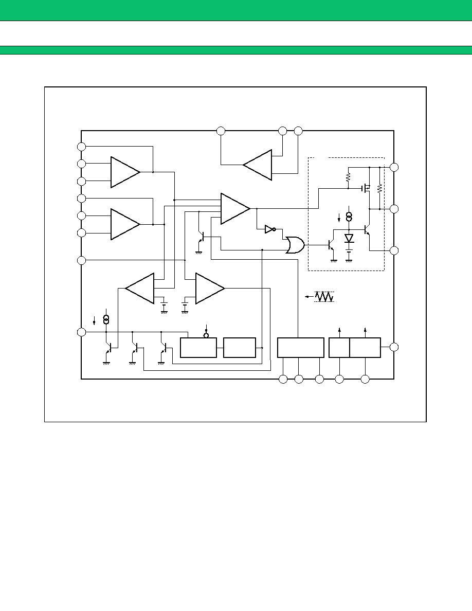
DESCRIPTION
The MB3832A is a pulse width modulation (PWM) DC/DC converter IC, incorporating a current detector amplifier
and error amplifiers (2 circuits) to control the output voltage and current independently. It is suitable for down-
conversion.
With an on-chip reference voltage generator, the MB3832A is best suited for use in applications such as lithium-
ion battery (1-cell to 3-cell) chargers.
s
FEATURES
∑ High precision reference voltage source: 2.5 V
±
0.5% (+25
∞
C)
: 2.5 V
±
1.0% (≠10
∞
C to +85
∞
C)
∑ High frequency operating capability: 500 kHz max.
∑ Wide operating supply voltage range: 3.6 V to 18 V
∑ On-chip current detector amplifier with wide in-phase input voltage range: 0 V to V
CC
∑ On-chip standby function
∑ On-chip triangular waveform oscillator capable of operating in external synchronization
∑ On-chip, timer-latch short-circuit protection circuit
∑ Internal totem-pole output stage supporting P-channel MOS FETs and PNP transistors
s
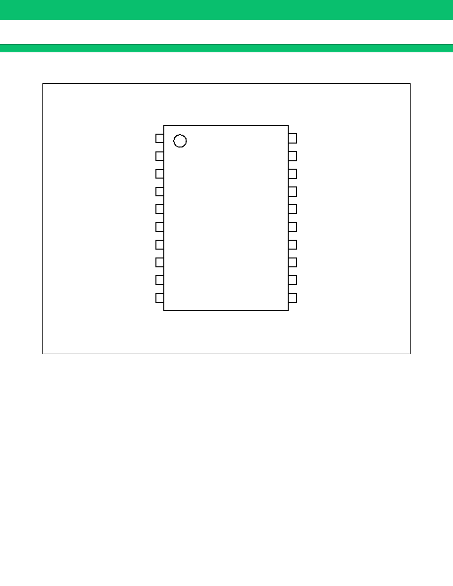
PACKAGE
20-pin plastic SSOP
(FPT-20P-M03)

3
MB3832A
s
PIN DESCRIPTION
I: Input pin, O: Output pin
Pin no.
Pin name
I/O
Descriptions
1
VREF
O
Reference voltage output pin
2
RT
--
Connection pin for triangular wave frequency setting resistor
3
CT
--
Connection pin for triangular wave frequency setting capacitor
4
SYNC
I
External synchronous signal input pin
5
CSCP
--
Connection pin for time constant setting capacitor for timer-latch short-
circuit protection circuit
6
FBI
O
Error amplifier 1 output pin
7
≠IN1
I
Error amplifier 1 inverted input pin
8
+IN1
I
Error amplifier 1 non-inverted input pin
9
≠INC
I
Current detector amplifier inverted input pin
10
+INC
I
Current detector amplifier non-inverted input pin
11
GND
--
Ground pin
12
COUT
O
Current detector amplifier output pin
13
+IN2
I
Error amplifier 2 non-inverted input pin
14
≠IN2
I
Error amplifier 2 inverted input pin
15
FB2
O
Error amplifier 2 output pin
16
DTC
I
Connection pin for dead time/soft start time setting resistor/capacitor
17
CTL
I
Power supply control input pin
"H" level: Active state
"L" level: Standby state
18
V
CC
--
Power supply pin
19
OUT
O
Totem-pole output pin
20
VE
--
Connector pin for output sink current setting resistor
5
MB3832A
s
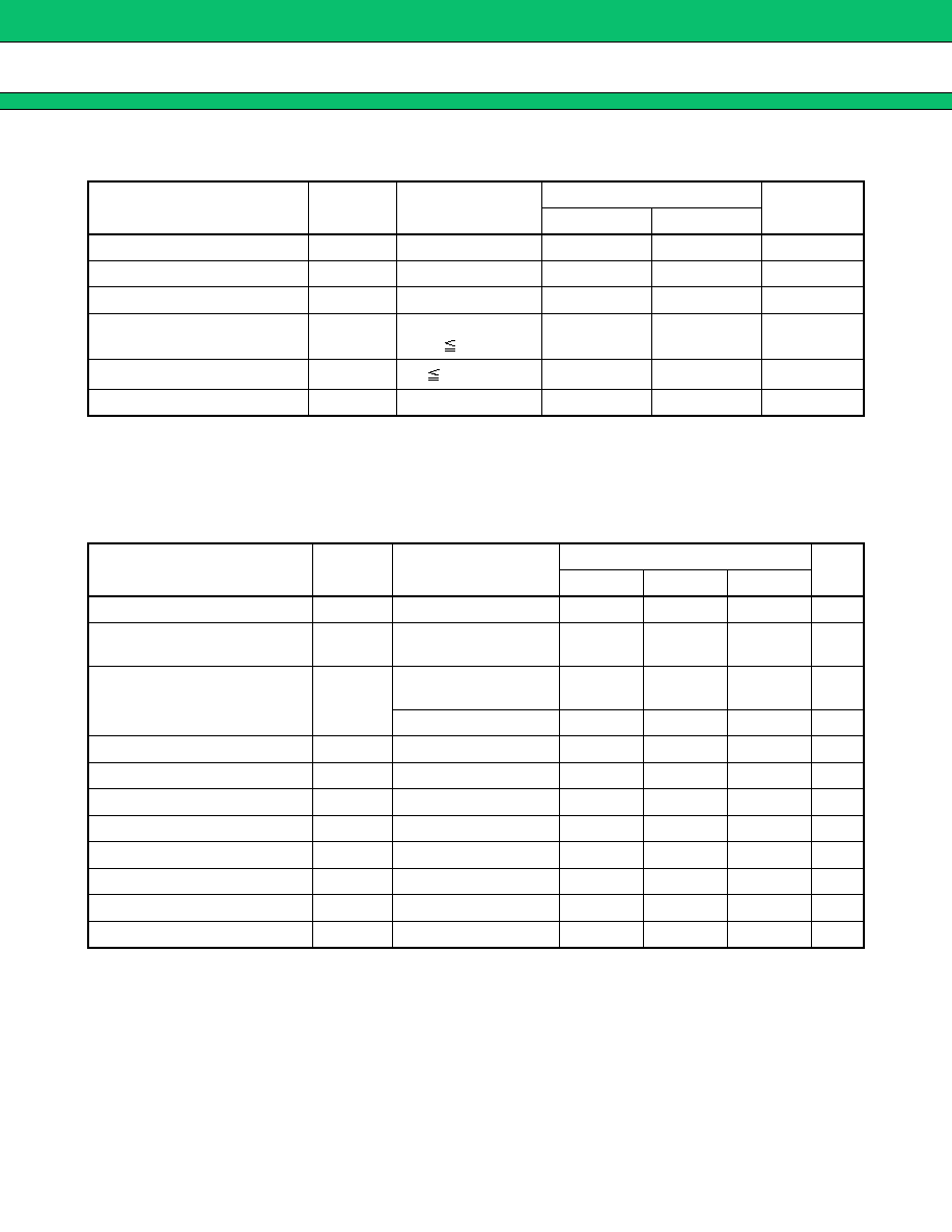
ABSOLUTE MAXIMUM RATINGS
* : When mounted on a 10 cm-square dual-sided epoxy base board
WARNING: Semiconductor devices can be permanently damaged by application of stress (voltage, current,
temperature, etc.) in excess of absolute maximum ratings. Do not exceed these ratings.
s
RECOMMENDED OPERATING CONDITIONS
WARNING: The recommended operating conditions are required in order to ensure the normal operation of the
semiconductor device. All of the device's electrical characteristics are warranted when the device is
operated within these ranges.
Always use semiconductor devices within their recommended operating condition ranges. Operation
outside these ranges may adversely affect reliability and could result in device failure.
No warranty is made with respect to uses, operating conditions, or combinations not represented on
the data sheet. Users considering application outside the listed conditions are advised to contact their
FUJITSU representatives beforehand.
Parameter
Symbol
Condition
Rating
Unit
Min.
Max.
Power supply voltage
V
CC
--
--
20
V
Control input voltage
V
CTL
--
--
20
V
Output current
I
O
OUT pin, DC
--
50
mA
Peak output current
I
O
OUT pin,
Duty
5%
--
600
mA
Allowable dissipation
P
D
Ta
+25
∞
C
--
540*
mW
Storage temperature
Tstg
--
≠55
+125
∞
C
Parameter
Symbol
Condition
Value
Unit
Min.
Typ.
Max.
Power supply voltage
V
CC
--
3.6
16
18
V
Reference voltage output
current
I
OR
--
≠1
--
0
mA
Input voltage
V
IN
+IN1, ≠IN1, +IN2,
≠IN2 pin
0
--
V
CC
≠ 0.9
V
+INC, ≠INC pin
0
--
V
CC
V
Control input voltage
V
CTL
CTL pin
0
--
18
V
SYNC input voltage
V
SYNC
SYNC pin
0
--
V
CC
V
Output current
I
O
OUT pin, DC
--
--
30
mA
Oscillatior frequency
f
OSC
--
10
200
500
kHz
Timing capacitance
C
T
--
100
390
2200
pF
Timing resistance
R
T
--
8.2
12
51
k
Short detection capacitance
C
SCP
--
--
0.1
1.0
µ
F
Operating temperature
Ta
--
≠30
+25
+85
∞
C