DS04-27700-3E
FUJITSU SEMICONDUCTOR
DATA SHEET
ASSP For Power Management Applications (Secondary battery)
Lithium Ion Battery Charger DC/DC Converter IC
(High Precision with Constant-current Function)
MB3813A/MB3833A/MB3843
s
DESCRIPTION
The FUJITSU MB3813A/33A/43 are pulse width modulation (PWM) DC/DC converter ICs with independent output
voltage and current setting capability.
The use of on-chip output setting resistance enables high precision output voltage control. Also, an output voltage
switching feature for use with either graphite-electrode or coke-electrode lithium-ion batteries makes this IC ideal
for internal battery chargers in notebook personal computers and similar applications.
s
FEATURES
� Output setting resistance is on-chip for high precision output voltage:
�
1.0%
� SEL pin enables output voltage selection
� High precision reference voltage source: 2.5 V
�
1.0%
� High frequency operating capability: max. 500 kHz
� On-chip current detector amplifier with wide in-phase input voltage range: 0 V to V
CC
(Continued)
s
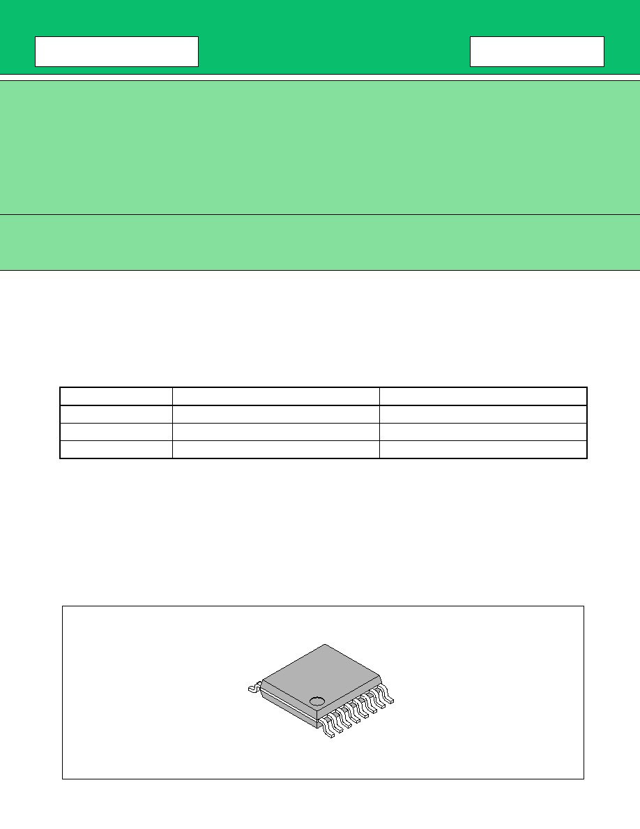
PACKAGE
Cell count
Output voltage
Part number
3-cell
12.6 V/12.3 V
MB3813A
2-cell
8.4 V/8.2 V
MB3833A
1-cell
4.2 V/4.1 V
MB3843
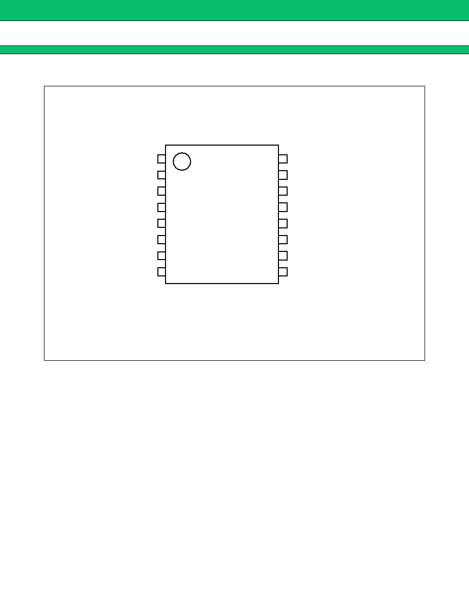
16-pin plastic SSOP
(FPT-16P-M05)
4
MB3813A/MB3833A/MB3843
s
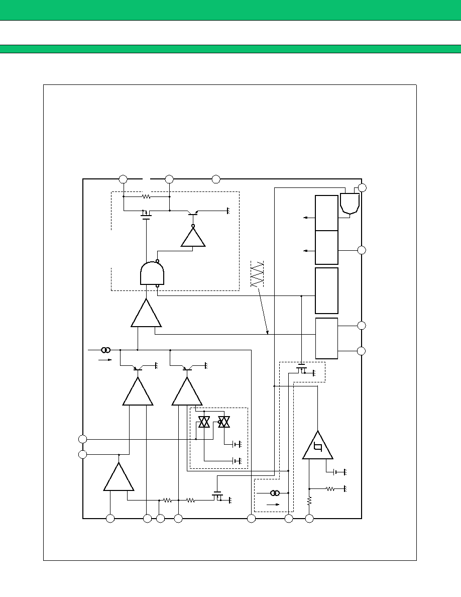
PIN DESCRIPTION
Pin no.
Symbol
I/O
Descriptions
1
Vin1
I
Input voltage detector block (VLDET) input pin
2
IN1
I
Current detector amplifier (Current Amp.) input pin
3
IN2
I
Output voltage feedback input pin
4
-IN2
I
Error amplifier (Error Amp.2) inverted input pin
5
-IN1
I
Error amplifier (Error Amp.1) inverted input pin
6
FB
O
Error amplifier (Error Amp.1, 2 common) output pin
7
CTL
I
Power supply control pin
An "L" level signal input to the CTL pin sets the IC in standby mode.
8
Vin2
I
DC/DC converter charging current setting input pin
9
VREF
O
Reference voltage output pin
10
SEL
I
Output voltage switching pin
"L" level output voltage: MB3813A 12.6 V
MB3833A 8.4 V
MB3843 4.2 V
"H" level output voltage: MB3813A 12.3 V
MB3833A 8.2 V
MB3843 4.1 V
11
CS
--
Soft start capacitor connection pin
12
RT
--
Triangular wave frequency setting resistor connection pin
13
CT
--
Triangular wave frequency setting capacitor connection pin
14
V
CC
--
Power supply pin
15
OUT
O
Totem-pole output pin
16
GND
--
Ground pin