 | –≠–ª–µ–∫—Ç—Ä–æ–Ω–Ω—ã–π –∫–æ–º–ø–æ–Ω–µ–Ω—Ç: MB3845 | –°–∫–∞—á–∞—Ç—å:  PDF PDF  ZIP ZIP |

DS04-27604-2E
FUJITSU SEMICONDUCTOR
DATA SHEET
ASSP For Power Supply Applications
Power Management 2-ch Switch IC
MB3842/MB3845
s
DESCRIPTION
The MB3842/3845 is a power management switch with built-in 2-channel low-on resistance (typ. 100m
) switch.
Output control is by means of a control signal, and the MB3842 is designed for high-active operation (output on
when EN is Hi), while the MB3845 is designed for low-active operation (output on when EN is low.)
To provide adaptability to a variety of operations, the MB3842/3845 features low input voltage (V
IN
>
2.5V)
operation and stable low-on resistance independent of input voltage. The switching current limit can be set from
100mA to 600mA by using external resistance, and when overcurrent conditions are detected the OC output goes
low to provide an external notification signal.
V
IN
is divided between the two channels, which operate independently of each other.
In addition, an off-state reverse current prevention function is provided to ensure accurate on/off switching action.
s
FEATURES
∑ Low on resistance switch (typ. 100m
)
∑ Low input voltage operation (2.5 V to 5.5 V)
∑ Switch current (max. 0.6 A)
∑ UVLO
:V
IN
threshold
2.3V/2.1 V hysteresis 200 mV
∑ ENABLE
:EN threshold
EN 1.4V/1.6 V for MB3842, EN 1/2 V
IN
for MB3845
:Power supply current at output off = 0
µ
A EN
<
0.8V for MB3842, EN
=
V
IN
for MB3845
∑ External setting for soft start time and switch current limit.
∑ Over-temperature detection (switch latched off), over-current detection (not latched)
∑ OC pin flag set following overcurrent detection, over-temperature detection, or UVLO detection.
∑ Reverse current prevention at OFF (V
IN
1.5 V)
∑ Either channel may be operated alone.
s
PACKAGE
20-pin plastic SSOP
(FPT-20P-M03)
2
MB3842/MB3845
s
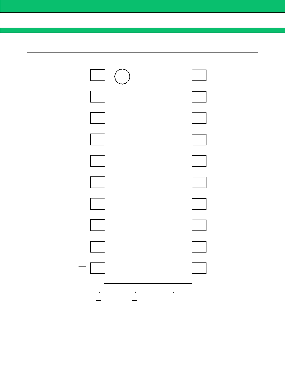
PIN ASSIGNMENT
20
19
18
17
16
15
14
13
12
11
GND
OC1
OUT1
OUT1
OUT1
OUT2
OUT2
OUT2
OC2
GND
1
2
3
4
5
6
7
8
9
10
EN1, EN1
SS1
CS1
VIN1
VIN1
VIN2
VIN2
CS2
SS2
EN2, EN2
SSOP-20P
(FPT-20P-M03)
EN Enable
CS Current Set
OC Over Current
EN Enable
SS Slow Start
The functions of pin 1 and pin 10 differ on the MB3842 and MB3845.
EN for MB3842/EN for MB3845
3
MB3842/MB3845
s
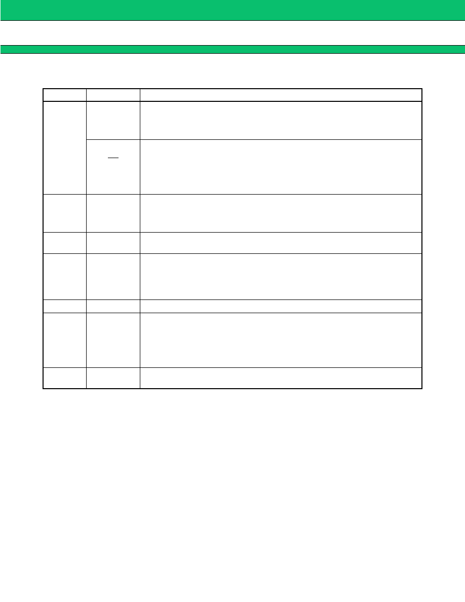
PIN DESCRIPTION
Pin no.
Symbol
Descriptions
1/10
EN
(MB3842)
Control signal input pin.
Set "H" to turn switch on, "L" to turn toff. At 0.8 V or less, the chip is in STBY state
and current consumption is less than 1
µ
A.
"L" level is 1.4V (typ), "H" level is 1.6V (typ), with 200mV (typ) hysteresis.
EN
(MB3845)
Control signal input pin.
Set "L" to turn switch on, "H" to turn off.
At "H" level = V
IN
, the chip is in STBY state and current consumption is less than
1
µ
A.
Normally used as CMOS inverter input, so that recommended use is "L" level at
GND +0.5V or less, and "H" level is V
IN
-0.5V or greater.
2/9
SS
Slow start setting pin. Used to adjust the switch on/off timing.
Add external capacitance to delay operation. Leave open when not in use.
In open mode voltages up to 12 V are present. Care should be taken in mounting
to prevent leakage current generation because high impedance is required.
3/8
CS
Current limit setting pin.
The limit current level is set by connecting this pin to external resistance.
4/5/6/7
VIN
Switch output pin.
An UVLO (V
IN
power monitor function) is provided so that when V
IN
reaches 2.3V
(typ.) or higher the OC pin voltage goes to "H" level. Also if the V
IN
voltage drops to
2.1 V (typ.) or lower the OC output goes to "L" state.
200mV (typ) hysteresis is provided.
11/20
GND
Ground pin.
12/19
OC
External notification pin.
When the switch is in on mode this pin normally outputs a "H" level signal, but
changes to "L" level when an overcurrent, overtemperature, or UVLO condition is
detected.
This is an open drain connection, and should be pulled up to high potential using
resistance.
13/14/15
16/17/18
OUT
Switching output pin.(N-ch MOSFET source)
4
MB3842/MB3845
s
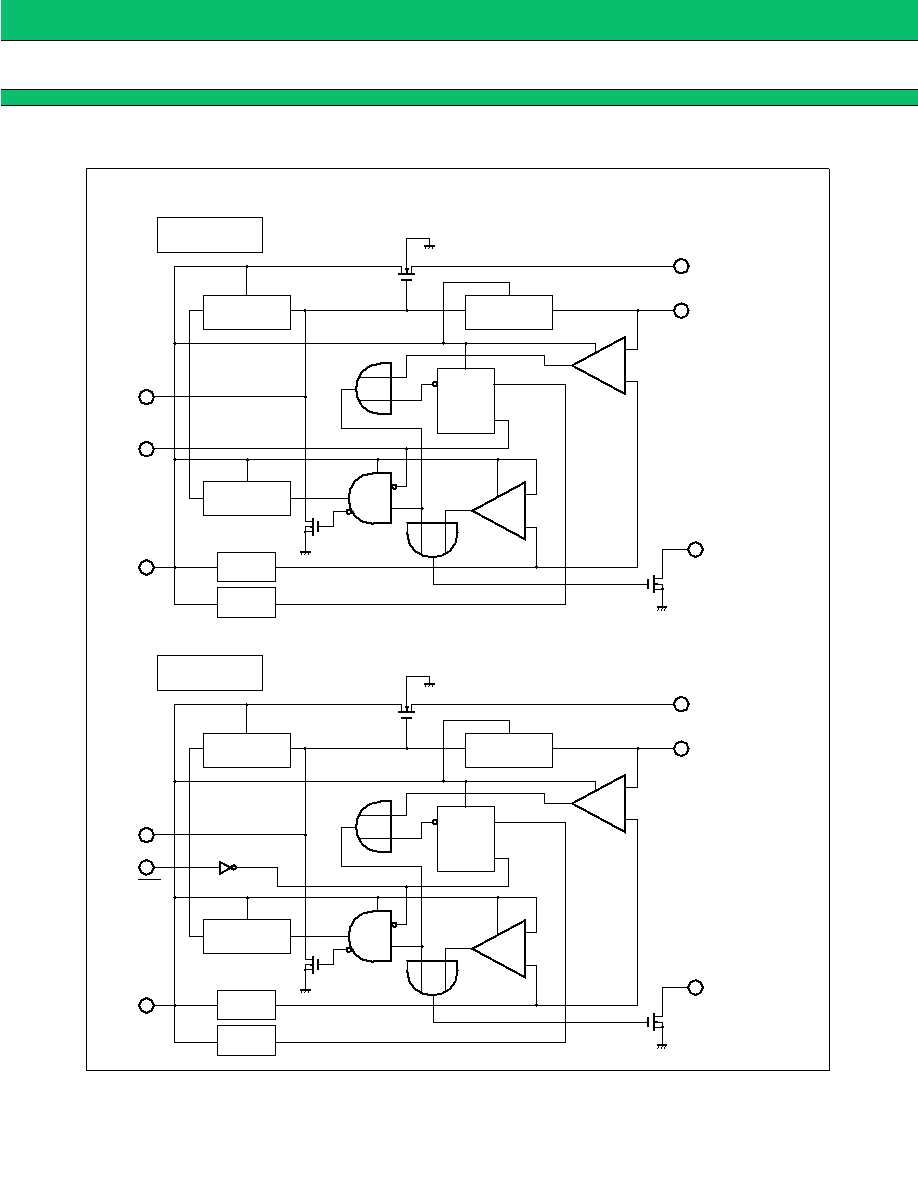
BLOCK DIAGRAM (for 1 channel)
SS1
EN1
VIN1
OSC1
BGR1
+
-
COMP
FF1
Q
S
R
OC1
OUT1
CS1
+
-
COMP
MB3842
SS1
EN1
VIN1
OSC1
BGR1
+
-
COMP
FF1
Q
S
R
OC1
OUT1
CS1
+
-
COMP
MB3845
Temperature
protection 1
Charge
pump1
Over current
detection 1
Charge
pump1
Over current
detection 1
Temperature
protection 1
5
MB3842/MB3845
s
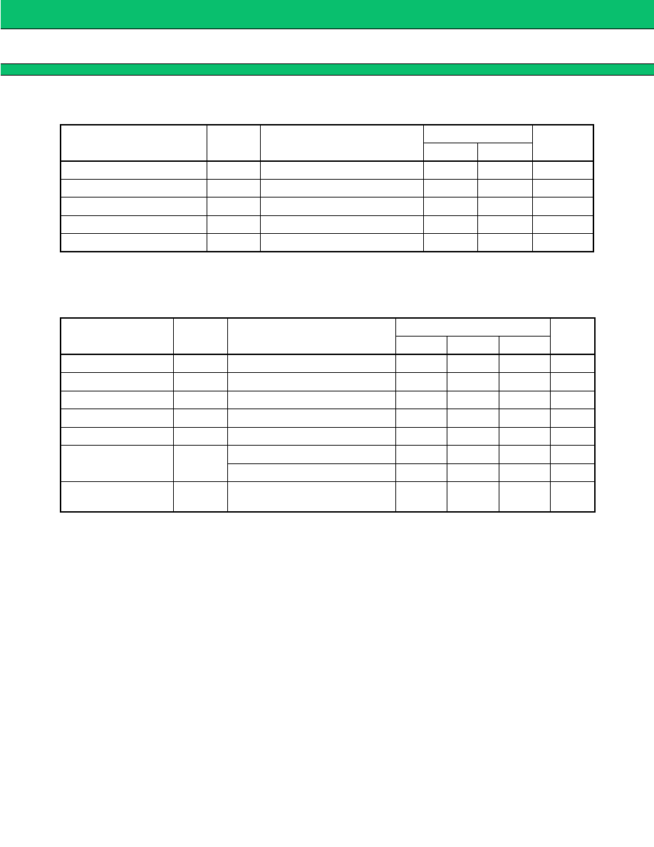
ABSOLUTE MAXIMUM RATINGS
WARNING: Semiconductor devices can be permanently damaged by application of stress (voltage, current,
temperature, etc.) in excess of absolute maximum ratings. Do not exceed these ratings.
s
RECOMMENDED OPERATING CONDITIONS
* : For C
SS
, R
LIM
settings, see "TYPICAL CHARACTERISTICS" and "FUNCTIONAL DESCRIPTION".
WARNING: The recommended operating conditions are required in order to ensure the normal operation of the
semiconductor device. All of the device's electrical characteristics are warranted when the device is
operated within these ranges.
Always use semiconductor devices within their recommended operating condition ranges. Operation
outside these ranges may adversely affect reliability and could result in device failure.
No warranty is made with respect to uses, operating conditions, or combinations not represented on
the data sheet. Users considering application outside the listed conditions are advised to contact their
FUJITSU representatives beforehand.
Parameter
Symbol
Condition
Rating
Unit
Max.
Min.
Input voltage
V
IN
--
≠0.3
7.0
V
ENABLE voltage
V
EN
--
≠0.3
7.0
V
Switch current
I
SW
--
--
1.8
A
Power dissipation
P
D
Ta = +85
∞
C
--
216
mW
Storage temperature
T
STG
--
≠55
+125
∞
C
Parameter
Symbol
Condition
Value
Unit
Min.
Typ.
Max.
Input voltage
V
IN
--
2.5
5.0
5.5
V
ENABLE voltage
V
EN
V
EN
V
IN
0
--
5.5
V
Switch current
I
SW
V
IN
= 2.5 V to 5.5 V
--
--
0.6
A
SS pin capacitance
C
SS
*
--
--
--
10
nF
OC sink current
I
OCS
V
IN
= 5.0 V, V
OC
= 0.4 V
2.0
5.0
--
mA
Current limit
resistance
R
LIM
*
V
IN
= 5.0 V (I
SW
= 0.6 A)
1.4
2.0
2.6
k
V
IN
= 5.0 V (I
SW
= 0.1 A)
3.6
6.2
9.1
k
Operating
temperature
T
OP
--
≠20
--
+85
∞
C