DS04-27703-3E
FUJITSU SEMICONDUCTOR
DATA SHEET
ASSP For Power Supply Applications (Lithium ion battery charger)
DC/DC Converter IC for Charging
MB3875/MB3877
s
DESCRIPTION
The MB3875 and MB3877 are charging DC/DC converter ICs suitable for down-conversion, which uses pulse
width modulation (PWM) for controlling the output voltage and current independently.
These ICs can dynamically control the secondary battery's charge current by detecting a voltage drop in an AC
adapter in order to keep its power constant (dynamically-controlled charging).
The charging method enables quick charging, for example, with the AC adapter during operation of a notebook PC.
With an on-chip output voltage setting resistor which allows the output voltage to be set at high precision, these
ICs are best suited as internal battery chargers for notebook PCs.
The MB3875 and MB3877 support 3-cell and 4-cell batteries, respectively.
These products are covered by US Patent Number 6,147,477.
s
FEATURES
� Detecting a voltage drop in the AC adapter and dynamically controlling the charge current (Dynamically-con-
trolled charging)
� High efficiency
: 95 %
� Wide range of operating supply voltages: 7 V to 25 V
� Output voltage precision (Output voltage setting resistor integrated): 0
�
0.8 % (Ta =
+
25
�
C)
(Continued)
s
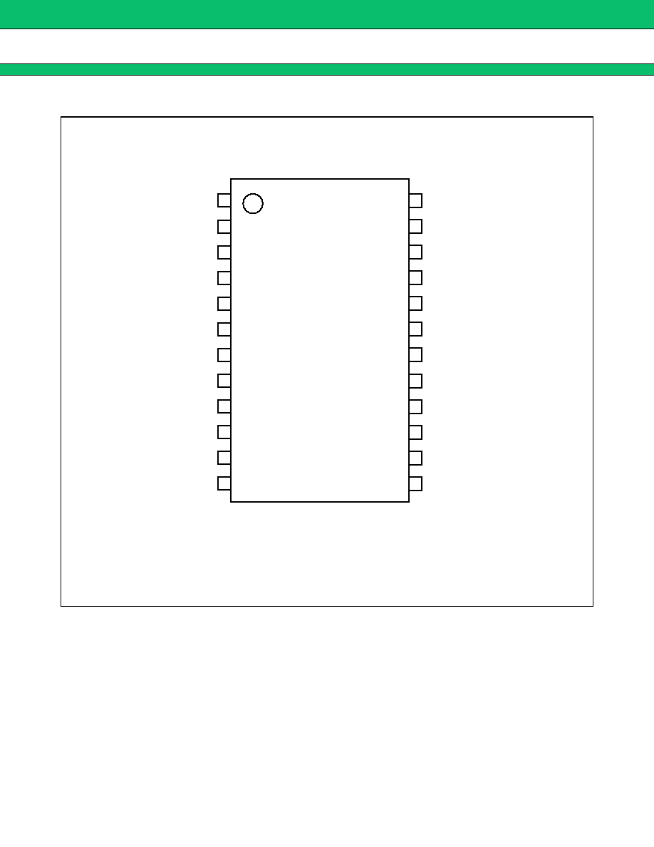
PACKAGE
24-pin plastic SSOP
(FPT-24P-M03)

MB3875/3877
2
(Continued)
� High precision reference voltage source: 4.2 V
�
0.8 %
� Support for frequency setting using an external resistor
(Frequency setting capacitor integrated) :100 kHz to 500 kHz
� On-chip current detector amplifier with wide in-phase input voltage range
: 0 V to V
CC
� On-chip standby current function: 0
�
A (Typ)
� On-chip soft-start function
� Internal totem-pole output stage supporting P-channel MOS FETs devices

MB3875/3877
4
s
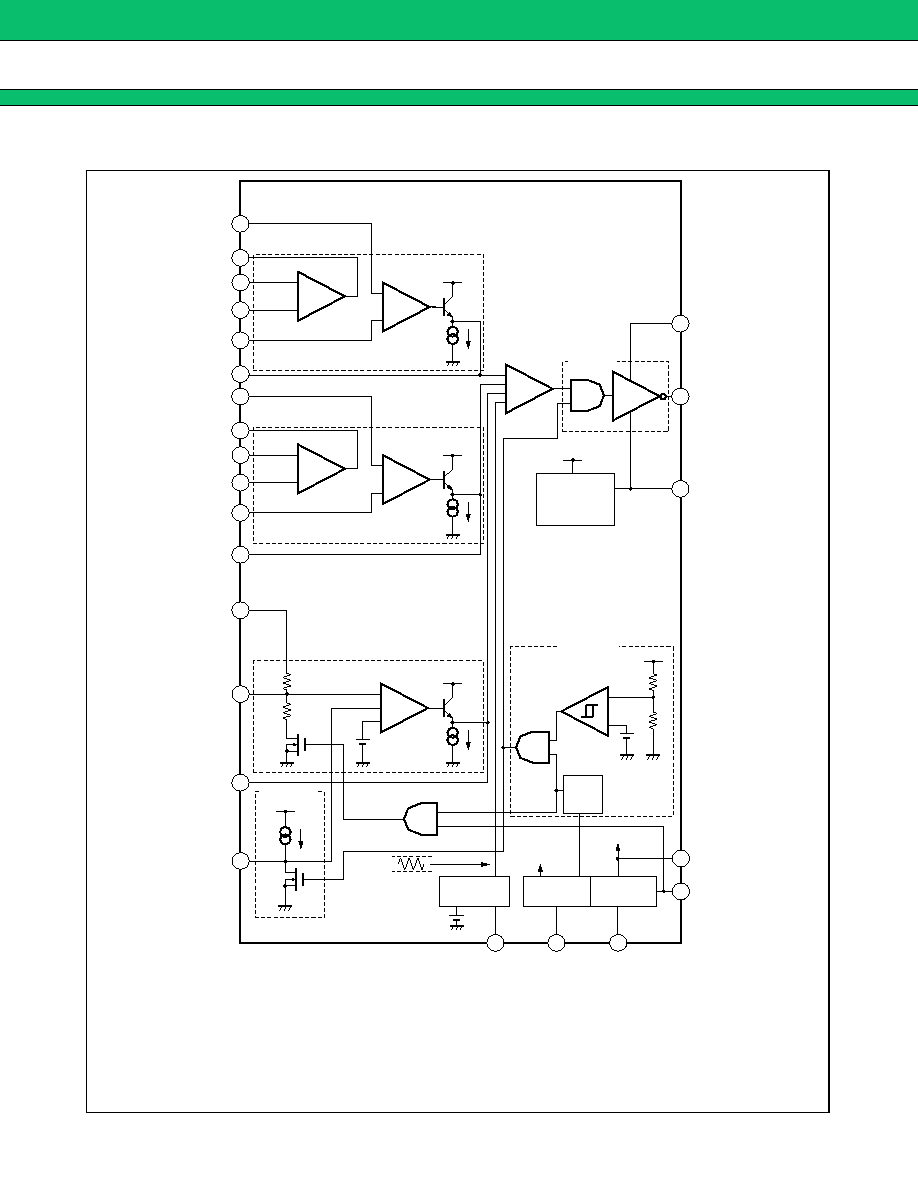
PIN DESCRIPTION
Pin No.
Symbol
I/O
Descriptions
1
�INC2
I
Current detection amplifier (Current Amp. 2) input pin.
2
IN3
I
DC/DC output voltage (charge voltage) input pin.
3
FB2
O
Error amplifier (Error Amp. 2) output pin.
4
OUTC2
O
Current detection amplifier (Current Amp. 2) output pin.
5
VREF
O
Reference voltage output pin.
6
�INE2
I
Error amplifier (Error Amp. 2) inverted input pin.
7
+INE2
I
Error amplifier (Error Amp. 2) non-inverted input pin.
8
+INE1
I
Error amplifier (Error Amp. 1) non-inverted input pin
9
FB1
O
Error amplifier (Error Amp. 1) output pin.
10
OUTC1
O
Current detection amplifier (Current Amp. 1) output pin.
11
�INE1
I
Error amplifier (Error Amp. 1) inverted input pin.
12
�INC1
I
Current detection amplifier (Current Amp. 1) input pin.
13
+INC1
I
Current detection amplifier (Current Amp. 1) input pin.
14
CTL
I
Power supply control pin.
Setting the CTL pin low places the IC in the standby mode.
15
FB3
O
Error amplifier (Error Amp. 3) output pin.
16
�INE3
I
Error amplifier (Error Amp. 3) inverted input pin.
17
RT
--
Triangular-wave oscillation frequency setting resistor connection pin.
18
V
CC
--
Power supply pin for reference power supply and control circuit.
19
VH
O
Power supply pin for FET drive circuit (VH = Vcc
-
5 V).
20
OUT
O
High-side FET gate drive pin.
21
V
CC
(O)
--
Output circuit power supply.
22
CS
--
Soft-start capacitor connection pin.
23
GND
--
Ground pin.
24
+INC2
I
Current detection amplifier (Current Amp. 2) input pin .