DS04-27708-2E
FUJITSU SEMICONDUCTOR
DATA SHEET
ASSP
for Power Supply Application (for secondary battery)
DC/DC Converter IC for Parallel Charging
of 3/4 cell Li-ion & NiMH Batteries
MB3879
s
DESCRIPTION
The MB3879 is a DC/DC converter IC for parallel charging of 3/4 cell Li-ion & NiMH batteries, which uses the
pulse-width modulation (PWM) for controlling output voltages and output currents independently.
This IC can dynamically control secondary batterie's charge current, which detects voltage dropping in an AC
adapter in order to keep its power constant (Dynamically controlled charging). This operation allows quick charging
by variable charging current in accordance with operating status of a notebook PC.
Moreover, the total current of the system current and control IC input current are detected, and control of the
secondary battery is enabled.
An efficient charge becomes possible because of the charge current comes in changeability according to the
operation state of notebook PC by this operation.
The IC also allows parallel charging that charges two batteries simultaneously, reducing charging time dramatically.
The IC, using a built-in output voltage setting resistor, allows high-precision setting of output voltages. With its
output-voltage switching function that is ready for both graphite-type and coke-type Li-ion batteries as well as
NiMH battery, the IC is best suited to a built-in charger of a notebook PC.
This product is covered by US Patent Number 6,147,477.
s
FEATURES
� Detecting a voltage dropping in the AC adapter, and dynamically controlling the charge current (Dynamically-
controlled charging)
� Detecting total current of system current and control-IC input current (Differential-charging)
(Continued)
s
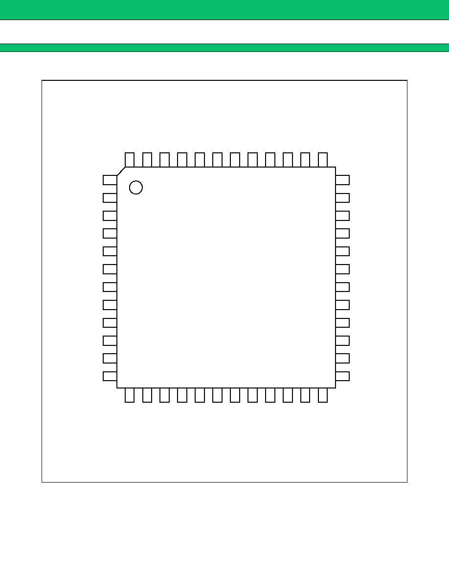
PACKAGE
48-pin plastic LQFP
(FPT-48P-M05)

MB3879
2
(Continued)
� Selection of output voltages by 4-bit decoder:
12.3V (3 cells: 4.1V), 12.6V (3 cells: 4.2V), 16.4V (4 cells: 4.1V), 16.8V (4 cells: 4.2V)
� High efficiency: 94% (using reverse current preventive diode)
� Wide range of power supply voltage: 8 V to 25 V
� Setting precision of output voltage (built-in output voltage setting resistor):
�
0.8% (Ta
=
+
25
�
C)
� Setting precision of charge current:
�
5%
� Setting of frequency for only external capacitor, using built-in frequency setting resistor.
� Oscillation frequency range: 100 kHz to 500 kHz
� Built-in current detect amplifier with wide range of in-phase input voltages: 0 V to Vcc
� Stand-by current: 0
�
A
� Built-in load-independent soft-start circuit
� Built-in charge mode detection function
� Built-in totem-pole outputs supporting Pch MOS FET

MB3879
4
s
PIN DESCRIPTION
(Continued)
Pin No.
Symbol
I/O
Descriptions
1
VCC
Power supply terminal
2
D0
I
VDD logic input terminal
3
D1
I
VDD logic input terminal
4
D2
I
VDD logic input terminal
5
D3
I
VDD logic input terminal
6
VSS
VDD logic ground terminal
7
CTL
I
Power supply control terminal. Setting "L" level on CTL terminal
places the IC in standby mode.
8
VDD
VDD logic power supply terminal
9
VB
O
Reference voltage output terminal
10
OUT-EV
O
Constant-voltage charging distinction signal output terminal
H level: Dynamically-controlled charging, Differential charging, or
Constant-voltage charging mode
L level: BATT1 or BATT2 Constant-voltage charging mode
11
OUT-EC
O
Constant-current charge distinction signal output terminal
H level: Dynamically-controlled charging, Differential charging, or
Constant-voltage charging mode
L level: BATT1 or BATT2 Constant-current charging mode
12
OUT-EA2
O
Differential-charging distinction signal output terminal
H level: Dynamically-controlled-charging, Constant-voltaging, or
Constant-current charging mode
L level: Differential-charging mode
13
OUT-EA1
O
Dynamically-controlled charging distinction signal output terminal
H level: Dynamically-controlled charging, Constant-voltage charging,
or Constant-current charging mode
L level: Dynamically-controlled charging mode
14
IN1
I
<BATT1> Current detection amplifier (Current Amp2) input terminal
Output voltage feedback input terminal
15
+
INC2
I
<BATT1> Current detection amplifier (Current Amp2) input terminal
16
FB3
O
<BATT1> Error amplifier (Error Amp3) output terminal
17
OUTC2
O
<BATT1> Current detection amplifier (Current Amp2) output terminal
18
-
INE3
I
<BATT1> Error amplifier (Error Amp3) inverted input terminal
19
+
INE3
I
<BATT1> Error amplifier (Error Amp3) non-inverted input terminal
20
FB6
O
<BATT1> Error amplifier (Error Amp6) output terminal
21
-
INE6
I
<BATT1> Error amplifier (Error Amp6) inverted input terminal
22
CS2
Soft-start capacitor connection terminal
23
CS1
Soft-start capacitor connection terminal
24
OUT
O
External FET gate driving terminal
25
VCCO
Driver block power supply terminal

MB3879
5
(Continued)
Pin No.
Symbol
I/O
Descriptions
26
VH
O
FET driver circuit power supply terminal (VH
=
VCC
-
6V)
27
GND0
Ground terminal
28
TEST
O
Internal reference voltage for setting charge voltage
29
-
INE5
I
<BATT2> Error amplifier (Error Amp5) inverted input terminal
30
FB5
O
<BATT2> Error amplifier (Error Amp5) output terminal
31
+
INE4
I
<BATT2> Error amplifier (Error Amp4) non-inverted input terminal
32
-
INE4
I
<BATT2> Error amplifier (Error Amp4) inverted input terminal
33
OUTC3
O
<BATT2> Current detection amplifier (Current Amp3) output terminal
34
FB4
O
<BATT2> Error amplifier (Error Amp4) output terminal
35
+
INC3
I
<BATT2> Current detection amplifier (Current Amp3) input terminal
36
IN2
I
<BATT2> Current detection amplifier (Current Amp3) input terminal
Output voltage feedback input terminal
37
CT
Triangular wave oscillation frequency setting capacitor connection
terminal
38
GND
Ground terminal
39
DTC
I
External duty control input terminal
40
+
INE2
I
Error amplifier (Error Amp2) non-inverted input terminal
41
-
INE2
I
Error amplifier (Error Amp2) inverted input terminal
42
FB2
O
Error amplifier (Error Amp2) output terminal
43
+
INE1
I
Error amplifier (Error Amp1) non-inverted input terminal
44
-
INE1
I
Error amplifier (Error Amp1) inverted input terminal
45
OUTC1
O
Current detection amplifier (Current Amp2) output terminal
46
FB1
O
Error amplifier (Error Amp1) output terminal
47
-
INC1
I
Current detection amplifier (Current Amp1) input terminal
48
+
INC1
I
Current detection amplifier (Current Amp1) input terminal