 | –≠–ª–µ–∫—Ç—Ä–æ–Ω–Ω—ã–π –∫–æ–º–ø–æ–Ω–µ–Ω—Ç: MB3887 | –°–∫–∞—á–∞—Ç—å:  PDF PDF  ZIP ZIP |
DS04-27709-4E
FUJITSU SEMICONDUCTOR
DATA SHEET
ASSP For Power Supply Applications (Secondary battery)
DC/DC Converter IC
for Charging Li-ion battery
MB3887
DESCRIPTION
The MB3887 is a DC/DC converter IC suitable for down-conversion, using pulse-width (PWM) charging and
enabling output voltage to be set to any desired level from one cell to four cells.
These ICs can dynamically control the secondary battery's charge current by detecting a voltage drop in an AC
adapter in order to keep its power constant (dynamically-controlled charging) .
The charging method enables quick charging, for example, with the AC adapter during operation of a notebook PC.
The MB3887 provides a broad power supply voltage range and low standby current as well as high efficiency,
making it ideal for use as a built-in charging device in products such as notebook PC.
This product is covered by US Patent Number 6,147,477.
FEATURES
∑ Detecting a voltage drop in the AC adapter and dynamically controlling the charge current
(Dynamically-controlled charging)
(Continued)
PACKAGE
24-pin plastic SSOP
(FPT-24P-M03)

MB3887
2
(Continued)
∑ Output voltage setting using external resistor
: 1 cell to 4 cells
∑ High efficiency
: 96
%
(VIN
=
19 V, Vo
=
16.8 V)
∑ Wide range of operating supply voltages
: 8 V to 25 V
∑ Output voltage setting accuracy
: 4.2 V
±
0.74
%
(Ta
=
-
10
∞
C to
+
85
∞
C , per cell)
∑ Charging current accuracy
:
±
5
%
∑ Built-in frequency setting capacitor enables frequency setting using external resistor only
∑ Oscillation frequency range
: 100 kHz to 500 kHz
∑ Built-in current detection amplifier with wide in-phase input voltage range : 0 V to VCC
∑ In standby mode, leave output voltage setting resistor open to prevent inefficient current loss
∑ Built-in standby current function
: 0
µ
A (standard)
∑ Built-in soft-start function independent of loads
∑ Built-in totem-pole output stage supporting P-channel MOS FET devices
MB3887
3
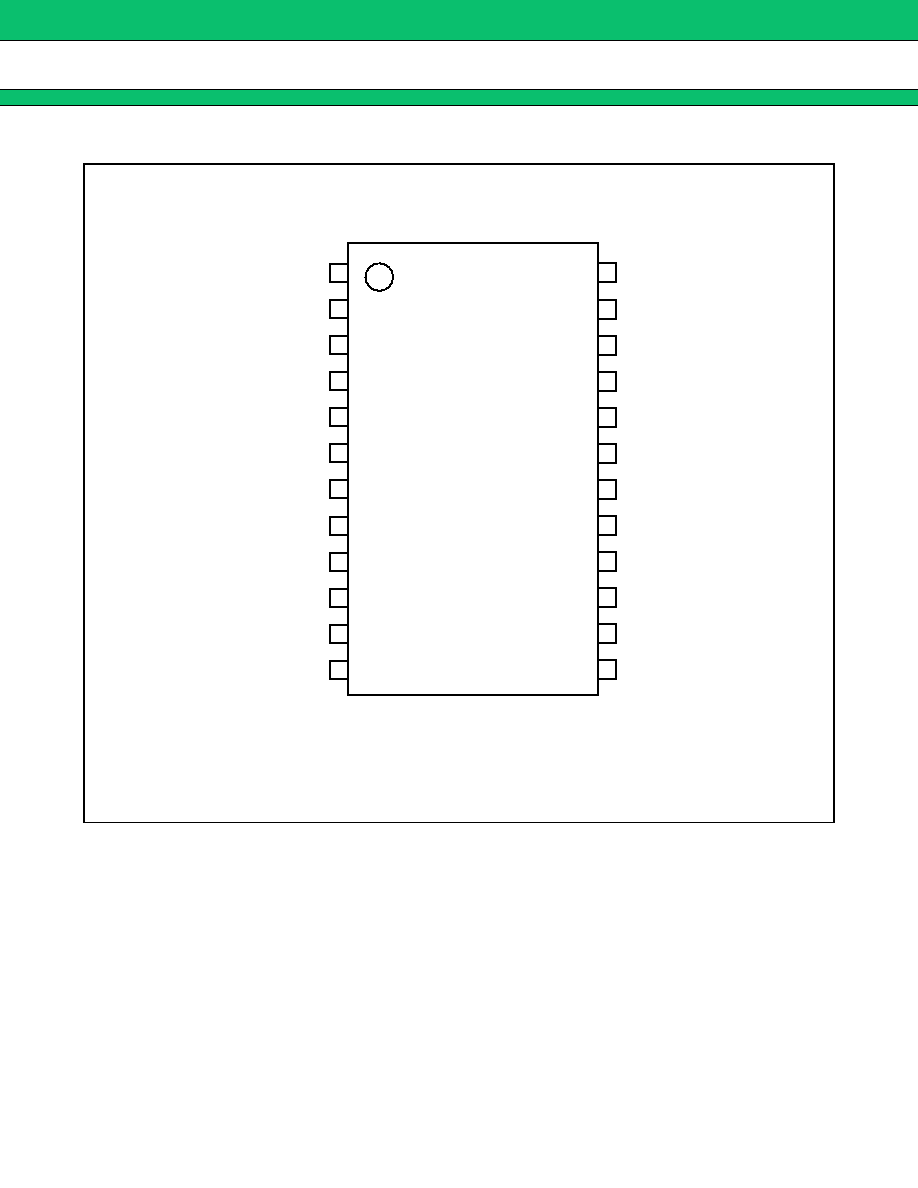
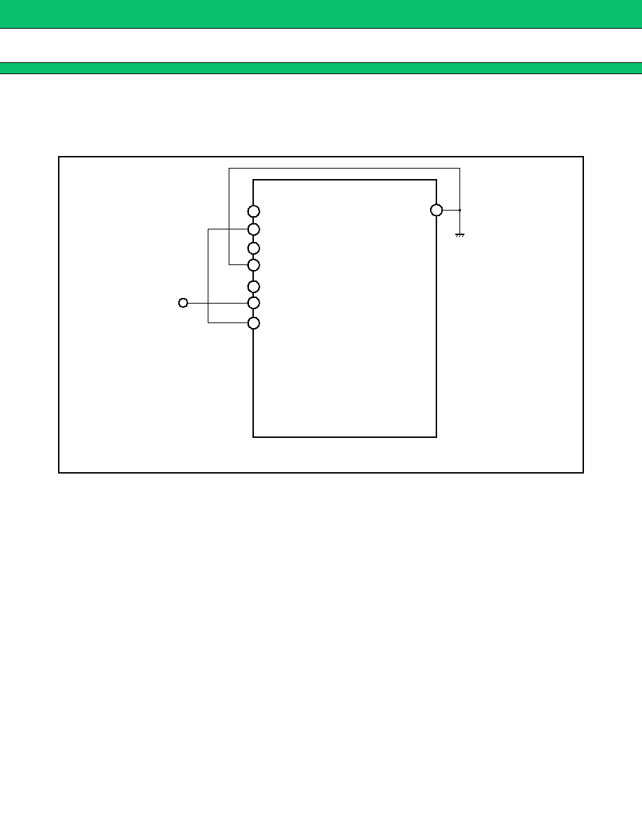
PIN ASSIGNMENT
(TOP VIEW)
(FPT-24P-M03)
1
2
3
4
5
6
7
8
9
10
11
12
-
INC2 :
OUTC2 :
+
INE2 :
-
INE2 :
FB2 :
VREF :
FB1 :
-
INE1 :
+
INE1 :
OUTC1 :
OUTD :
-
INC1 :
24
23
22
21
20
19
18
17
16
15
14
13
:
+
INC2
: GND
: CS
: VCC (O)
: OUT
: VH
: VCC
: RT
:
-
INE3
: FB3
: CTL
:
+
INC1

MB3887
4
PIN DESCRIPTION
Pin No.
Symbol
I/O
Descriptions
1
-
INC2
I
Current detection amplifier (Current Amp2) input terminal.
2
OUTC2
O
Current detection amplifier (Current Amp2) output terminal.
3
+
INE2
I
Error amplifier (Error Amp2) non-inverted input terminal.
4
-
INE2
I
Error amplifier (Error Amp2) inverted input terminal.
5
FB2
O
Error amplifier (Error Amp2) output terminal.
6
VREF
O
Reference voltage output terminal.
7
FB1
O
Error amplifier (Error Amp1) output terminal.
8
-
INE1
I
Error amplifier (Error Amp1) inverted input terminal
9
+
INE1
I
Error amplifier (Error Amp1) non-inverted input terminal.
10
OUTC1
O
Current detection amplifier (Current Amp1) output terminal.
11
OUTD
O
With IC in standby mode, this terminal is set to "Hi-Z" to prevent loss
of current through output voltage setting resistance.
Set CTL terminal to "H" level to output "L" level.
12
-
INC1
I
Current detection amplifier (Current Amp1) input terminal.
13
+
INC1
I
Current detection amplifier (Current Amp1) input terminal.
14
CTL
I
Power supply control terminal.
Setting the CTL terminal at "L" level places the IC in the standby
mode.
15
FB3
O
Error amplifier (Error Amp3) output terminal.
16
-
INE3
I
Error amplifier (Error Amp3) inverted input terminal.
17
RT
Triangular-wave oscillation frequency setting resistor connection
terminal.
18
VCC
Power supply terminal for reference power supply and control circuit.
19
VH
O
Power supply terminal for FET drive circuit (VH
=
VCC
-
6 V) .
20
OUT
O
External FET gate drive terminal.
21
VCC (O)
Output circuit power supply terminal.
22
CS
Soft-start capacitor connection terminal.
23
GND
Ground terminal.
24
+
INC2
I
Current detection amplifier (Current Amp2) input terminal.
MB3887
5
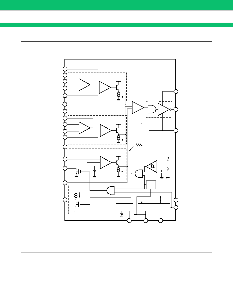
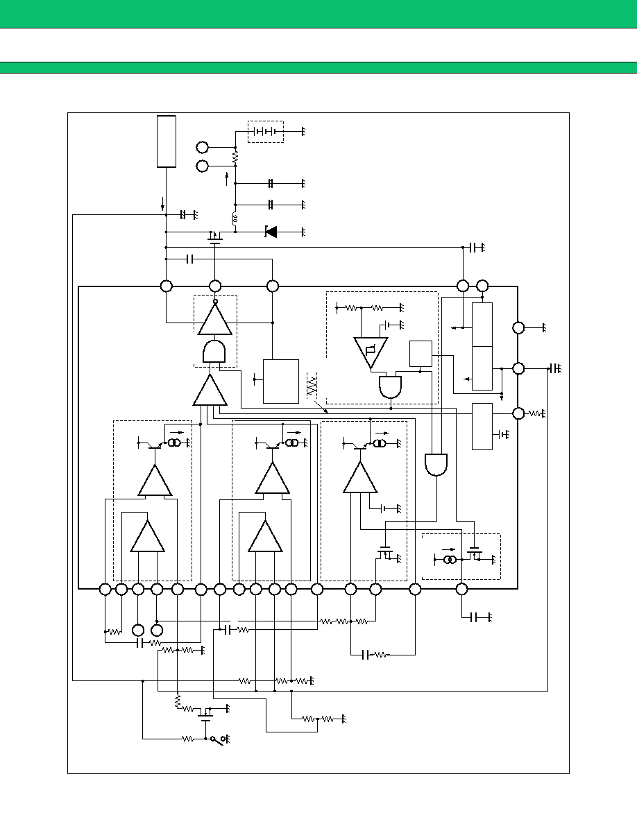
BLOCK DIAGRAM
+
-
-
+
8
10
13
12
9
+
-
-
+
4
2
24
1
3
◊
20
◊
20
+
+
+
-
5
20
21
19
-
+
+
+
-
11
16
22
17
6
23
14
18
<Current Amp1>
<Error Amp1>
7
VREF
<Current Amp2>
<Error Amp2>
VREF
<Error Amp3>
VREF
VREF
VREF
5.0 V
4.2 V
10
µ
A
15
<SOFT>
2.5 V
1.5 V
<OUT>
<UVLO>
<OSC>
Bias
Voltage
<VH>
<REF>
<CTL>
<PWM Comp.>
Drive
VCC
(V
CC
-
6 V)
(VCC UVLO)
VCC
VCC
VCC
CTL
215 k
35 k
0.91 V
(0.77 V)
VREF
UVLO
4.2 V
bias
-
INC2
OUTD
FB2
OUTC2
VREF
-
INE2
+
INE2
+
INE1
FB1
OUTC1
-
INE1
-
INC1
+
INC2
GND
CS
VCC (O)
OUT
VH
RT
-
INE3
FB3
+
INC1
45 pF

MB3887
6
ABSOLUTE MAXIMUM RATINGS
*1 : The package is mounted on the dual-sided epoxy board (10 cm
◊
10 cm) .
*2 : Refer to " THE SEQUENCE OF THE START-UP AND OFF OF THE POWER SUPPLY" for details.
WARNING: Semiconductor devices can be permanently damaged by application of stress (voltage, current,
temperature, etc.) in excess of absolute maximum ratings. Do not exceed these ratings.
Parameter
Symbol
Conditions
Rating
Unit
Min
Max
Power supply voltage
V
CC
VCC, VCC (O) terminal*
2
28
V
Output current
I
OUT
60
mA
Peak output current
I
OUT
Duty
5
%
(t
=
1
/
f
OSC
◊
Duty)
700
mA
Power dissipation
P
D
Ta
+
25
∞
C
740*
1
mW
Storage temperature
T
STG
-
55
+
125
∞
C

MB3887
7
RECOMMENDED OPERATING CONDITIONS
* : Refer to " THE SEQUENCE OF THE START-UP AND OFF OF THE POWER SUPPLY" for details.
WARNING: The recommended operating conditions are required in order to ensure the normal operation of the
semiconductor device. All of the device's electrical characteristics are warranted when the device is
operated within these ranges.
Always use semiconductor devices within their recommended operating condition ranges. Operation
outside these ranges may adversely affect reliability and could result in device failure.
No warranty is made with respect to uses, operating conditions, or combinations not represented on
the data sheet. Users considering application outside the listed conditions are advised to contact their
FUJITSU representatives beforehand.
Parameter
Symbol
Conditions
Value
Unit
Min
Typ
Max
Power supply voltage
V
CC
VCC, VCC (O) terminal*
8
25
V
Reference voltage output
current
I
REF
-
1
0
mA
VH terminal output current
I
VH
0
30
mA
Input voltage
V
INE
-
INE1 to
-
INE3,
+
INE1,
+
INE2 terminal
0
V
CC
-
1.8
V
V
INC
+
INC1,
+
INC2,
-
INC1,
-
INC2 terminal
0
V
CC
V
OUTD terminal output voltage
V
OUTD
0
17
V
OUTD terminal output current
I
OUTD
0
2
mA
CTL terminal input voltage
V
CTL
0
25
V
Output current
I
OUT
-
45
+
45
mA
Peak output current
I
OUT
Duty
5
%
(t
=
1
/
fosc
◊
Duty)
-
600
+
600
mA
Oscillation frequency
f
OSC
100
290
500
kHz
Timing resistor
R
T
27
47
130
k
Soft-start capacitor
C
S
0.022
1.0
µ
F
VH terminal capacitor
C
VH
0.1
1.0
µ
F
Reference voltage output
capacitor
C
REF
0.1
1.0
µ
F
Operating ambient
temperature
Ta
-
30
+
25
+
85
∞
C
MB3887
8
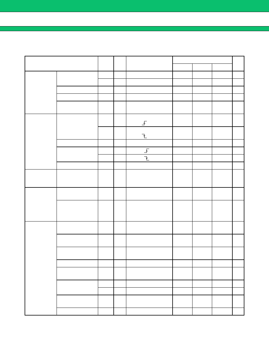
ELECTRICAL CHARACTERISTICS
(Ta
=
+
25
∞
C, VCC
=
19 V, VCC (O)
=
19 V, VREF
=
0 mA)
* : Standard design value.
(Continued)
Parameter
Sym-
bol
Pin
No.
Conditions
Value
Unit
Min
Typ
Max
1.
Reference
voltage block
[REF]
Output voltage
V
REF1
6
Ta
=
+
25
∞
C
4.967
5.000
5.041
V
V
REF2
6
Ta
=
-
10
∞
C to
+
85
∞
C
4.95
5.00
5.05
V
Input stability
Line
6
VCC
=
8 V to 25 V
3
10
mV
Load stability
Load
6
VREF
=
0 mA to
-
1 mA
1
10
mV
Short-circuit output
current
Ios
6
VREF
=
1 V
-
50
-
25
-
12
mA
2.
Under voltage
lockout protec-
tion circuit
block
[UVLO]
Threshold voltage
V
TLH
18
VCC
=
VCC (O) ,
VCC
=
6.2
6.4
6.6
V
V
THL
18
VCC
=
VCC (O) ,
VCC
=
5.2
5.4
5.6
V
Hysteresis width
V
H
18
VCC
=
VCC (O)
1.0*
V
Threshold voltage
V
TLH
6
VREF
=
2.6
2.8
3.0
V
V
THL
6
VREF
=
2.4
2.6
2.8
V
Hysteresis width
V
H
6
0.2
V
3.
Soft-start block
[SOFT]
Charge current
I
CS
22
-
14
-
10
-
6
µ
A
4.
Triangular
waveform os-
cillator circuit
block
[OSC]
Oscillation
frequency
f
OSC
20
RT
=
47 k
260
290
320
kHz
Frequency
temperature
stability
f/fdt
20
Ta
=
-
30
∞
C to
+
85
∞
C
1*
%
5-1.
Error amplifier
block
[Error Amp1,
Error Amp2]
Input offset voltage
V
IO
3, 4,
8, 9
FB1
=
FB2
=
2 V
1
5
mV
Input bias current
I
B
3, 4,
8, 9
-
100
-
30
nA
In-phase input
voltage range
V
CM
3, 4,
8, 9
0
V
CC
-
1.8
V
Voltage gain
A
V
5, 7 DC
100*
dB
Frequency
bandwidth
BW
5, 7 AV
=
0 dB
2*
MHz
Output voltage
V
FBH
5, 7
4.7
4.9
V
V
FBL
5, 7
20
200
mV
Output source
current
I
SOURCE
5, 7 FB1
=
FB2
=
2 V
-
2
-
1
mA
Output sink current
I
SINK
5, 7 FB1
=
FB2
=
2 V
150
300
µ
A

MB3887
9
(Ta
=
+
25
∞
C, VCC
=
19 V, VCC (O)
=
19 V, VREF
=
0 mA)
* : Standard design value
(Continued)
Parameter
Sym-
bol
Pin
No.
Conditions
Value
Unit
Min
Typ
Max
5-2.
Error amplifier
block
[Error Amp3]
Threshold voltage
V
TH1
16
FB3
=
2 V, Ta
=
+
25
∞
C
4.183
4.200
4.225
V
V
TH2
16
FB3
=
2 V,
Ta
=
-
10
∞
C to
+
85
∞
C
4.169
4.200
4.231
V
Input current
I
INE3
16
-
INE3
=
0 V
-
100
-
30
nA
Voltage gain
A
V
15
DC
100*
dB
Frequency
bandwidth
BW
15
AV
=
0 dB
2*
MHz
Output voltage
V
FBH
15
4.7
4.9
V
V
FBL
15
20
200
mV
Output source
current
I
SOURCE
15
FB3
=
2 V
-
2
-
1
mA
Output sink current
I
SINK
15
FB3
=
2 V
150
300
µ
A
OUTD terminal
output leak current
I
LEAK
11
OUTD
=
17 V
0
1
µ
A
OUTD terminal
output ON resistor
R
ON
11
OUTD
=
1 mA
35
50
6.
Current detec-
tion amplifier
block
[Current
Amp1, Current
Amp2]
Input offset voltage
V
IO
1,
12,
13,
24
+
INC1
=
+
INC2
=
-
INC1
=
-
INC2
=
3 V to VCC
-
3
+
3
mV
Input current
I
+
INCH
13,
24
+
INC1
=
+
INC2
=
3 V to VCC,
V
IN
=
-
100 mV
20
30
µ
A
I
-
INCH
1, 12
+
INC1
=
+
INC2
=
3 V to VCC,
Vin
=
-
100 mV
0.1
0.2
µ
A
I
+
INCL
13,
24
+
INC1
=
+
INC2
=
0 V,
Vin
=
-
100 mV
-
180
-
120
µ
A
I
-
INCL
1, 12
+
INC1
=
+
INC2
=
0 V,
Vin
=
-
100 mV
-
195
-
130
µ
A

MB3887
10
(Ta
=
+
25
∞
C, VCC
=
19 V, VCC (O)
=
19 V, VREF
=
0 mA)
* : Standard design value
(Continued)
Parameter
Sym-
bol
Pin
No.
Conditions
Value
Unit
Min
Typ
Max
6.
Current
detection
amplifier block
[Current Amp1,
Current Amp2]
Current detection
voltage
V
OUTC1
2, 10
+
INC1
=
+
INC2
=
3 V to VCC,
Vin
=
-
100 mV
1.9
2.0
2.1
V
V
OUTC2
2, 10
+
INC1
=
+
INC2
=
3 V to VCC,
Vin
=
-
20 mV
0.34
0.40
0.46
V
V
OUTC3
2, 10
+
INC1
=
+
INC2
=
0 V to 3 V,
Vin
=
-
100 mV
1.8
2.0
2.2
V
V
OUTC4
2, 10
+
INC1
=
+
INC2
=
0 V to 3 V,
Vin
=
-
20 mV
0.2
0.4
0.6
V
In-phase input
voltage range
V
CM
1,
12,
13,
24
0
V
CC
V
Voltage gain
A
V
2, 10
+
INC1
=
+
INC2
=
3 V to VCC,
Vin
=
-
100 mV
19
20
21
V/V
Frequency
bandwidth
BW
2, 10 AV
=
0 dB
2*
MHz
Output voltage
V
OUTCH
2, 10
4.7
4.9
V
V
OUTCL
2, 10
20
200
mV
Output source
current
I
SOURCE
2, 10 OUTC1
=
OUTC2
=
2 V
-
2
-
1
mA
Output sink cur-
rent
I
SINK
2, 10 OUTC1
=
OUTC2
=
2 V
150
300
µ
A
7.
PWM
comparator
block
[PWM Comp.]
Threshold voltage
V
TL
5, 7,
15
Duty cycle
=
0
%
1.4
1.5
V
V
TH
5, 7,
15
Duty cycle
=
100
%
2.5
2.6
V

MB3887
11
(Continued)
(Ta
=
+
25
∞
C, VCC
=
19 V, VCC (O)
=
19 V, VREF
=
0 mA)
* : Standard design value
Parameter
Sym-
bol
Pin
No.
Conditions
Value
Unit
Min
Typ
Max
8.
Output block
[OUT]
Output source
current
I
SOURCE
20
OUT
=
13 V, Duty
5
%
(t
=
1
/
f
OSC
◊
Duty)
-
400*
mA
Output sink
current
I
SINK
20
OUT
=
19 V, Duty
5
%
(t
=
1
/
f
OSC
◊
Duty)
400*
mA
Output ON
resistor
R
OH
20
OUT
=
-
45 mA
6.5
9.8
R
OL
20
OUT
=
45 mA
5.0
7.5
Rise time
tr1
20
OUT
=
3300 pF
(Si4435
◊
1)
50*
ns
Fall time
tf1
20
OUT
=
3300 pF
(Si4435
◊
1)
50*
ns
9.
Control block
[CTL]
CTL input voltage
V
ON
14
IC Active mode
2
25
V
V
OFF
14
IC Standby mode
0
0.8
V
Input current
I
CTLH
14
CTL
=
5 V
100
150
µ
A
I
CTLL
14
CTL
=
0 V
0
1
µ
A
10.
Bias voltage
block
[VH]
Output voltage
V
H
19
VCC
=
VCC (O)
=
8 V to 25 V,
VH
=
0 to 30 mA
V
CC
-
6.5 V
CC
-
6.0 V
CC
-
5.5
V
11.
General
Standby current
I
CCS
18
VCC
=
VCC (O) ,
CTL
=
0 V
0
10
µ
A
Power supply cur-
rent
I
CC
18
VCC
=
VCC (O) ,
CTL
=
5 V
8
12
mA
MB3887
12
TYPICAL CHARACTERISTICS
(Continued)
6
5
4
3
2
1
0
0
5
10
15
20
25
Ta
= +
25
∞
C
CTL
=
5 V
6
5
4
3
2
1
0
0
5
10
15
20
25
Ta
= +
25
∞
C
CTL
=
5 V
VREF
=
0 mA
6
5
4
3
2
1
0
0
5
10
15
20
25
30
Ta
= +
25
∞
C
VCC
=
19 V
CTL
=
5 V
5.08
5.06
5.04
5.02
5.00
4.98
4.96
4.94
4.92
-
40
-
20
0
20
40
60
80
100
VCC
=
19 V
CTL
=
5 V
1000
900
800
700
600
500
400
300
200
100
0
10
9
8
7
6
5
4
3
2
1
0
0
5
10
15
20
25
V
REF
I
CTL
Ta
= +
25
∞
C
VCC
=
19 V
Power supply current I
CC
(mA)
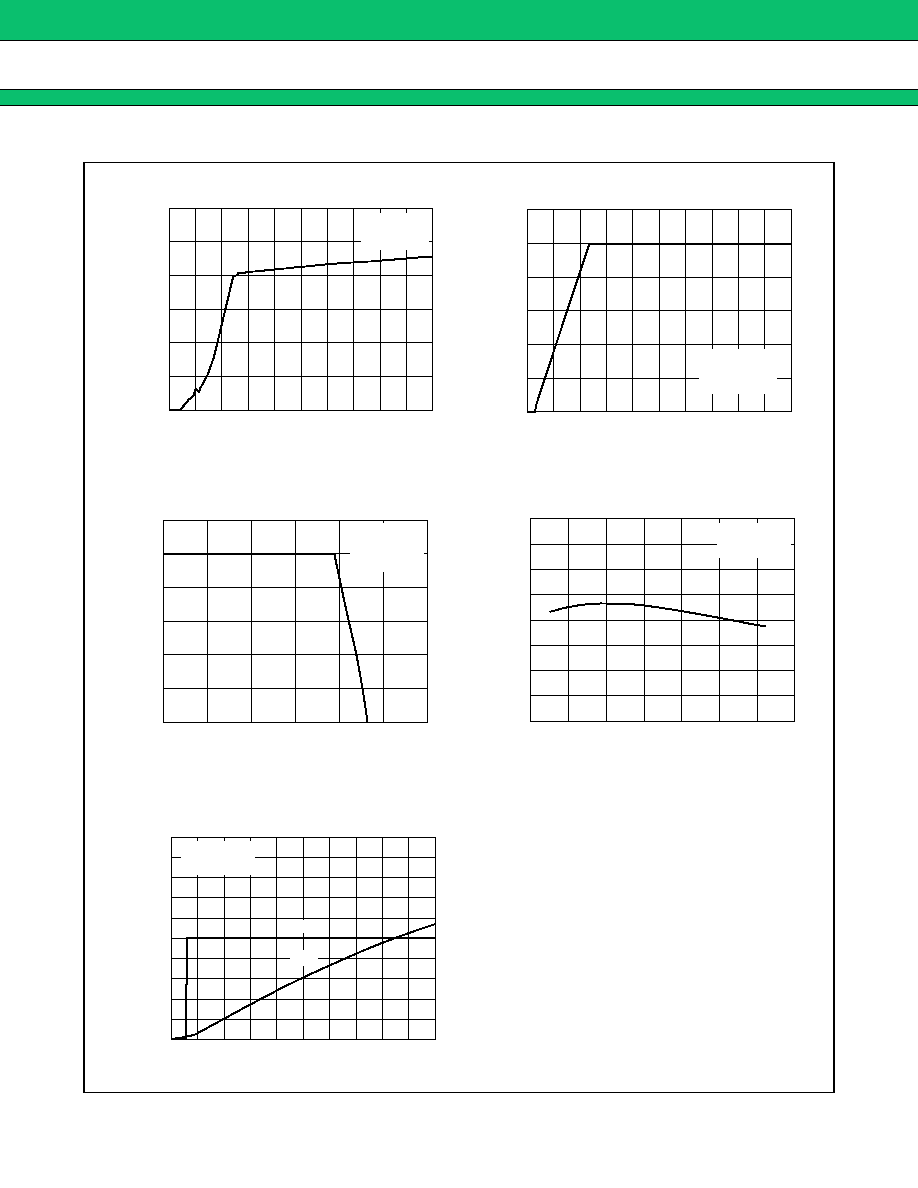
Power supply current vs. Power supply voltage
Power supply voltage V
CC
(V)
Reference voltage V
REF
(V)
Power supply voltage V
CC
(V)
Reference voltage vs. Power supply voltage
Reference voltage V
REF
(V)
Reference voltage output current I
REF
(mA)
Reference voltage
vs. Reference voltage output current
Reference voltage
vs. Operating ambient temperature
Reference voltage V
REF
(V)
Operating ambient temperature Ta (
∞
C)
CTL terminal current, Reference voltage
vs. CTL terminal voltage
CTL ter
m
inal current I
CT
L
(
µ
A)
CTL terminal voltage V
CTL
(V)
Reference voltage V
REF
(V)
MB3887
13
(Continued)
1 M
100 k
10 k
10
100
1000
Ta
= +
25
∞
C
VCC
=
19 V
CTL
=
5 V
340
330
320
310
300
290
280
270
260
0
5
10
15
20
25
Ta
= +
25
∞
C
CTL
=
5 V
RT
=
47 k
320
315
310
305
300
295
290
285
280
275
270
265
260
-
40
-
20
0
20
40
60
80
100
VCC
=
19 V
CTL
=
5 V
RT
=
47 k
4.25
2.24
4.23
2.22
4.21
4.20
4.19
4.18
4.17
4.16
4.15
-
40
-
20
0
20
40
60
80
100
VCC
=
19 V
CTL
=
5 V
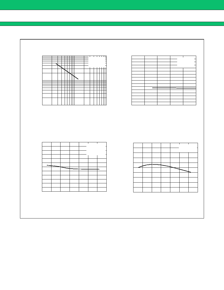
Triangular wave oscillation frequency
vs. Timing resistor
Triangular wave oscillation
frequency f
OSC
(Hz)
Timing resistor R
T
(k
)
Triangular wave oscillation frequency
vs. Power supply voltage
Triangular wave oscillation
frequency f
OS
C
(kHz)
Power supply voltage V
CC
(V)
Triangular wave oscillation frequency
vs. Operating ambient temperature
Triangular wave oscillation
frequency f
OSC
(kHz)
Operating ambient temperature Ta (
∞
C)
Error amplifier threshold voltage
vs. Operating ambient temperature
Error amplifier threshold
voltage V
TH
(V)
Operating ambient temperature Ta (
∞
C)
MB3887
14
(Continued)
-
+
7
8
9
+
OUT
IN
(5)
(4)
(3)
240 k
2.4 k
10 k
10 k
10 k
10 k
Error Amp1
(Error Amp2)
4.2 V
VCC
=
19 V
1
µ
F
Ta
= +
25
∞
C
A
V
40
20
0
-
20
-
40
180
90
0
-
90
-
180
1 k
10 k
100 k
1 M
10 M
-
+
+
15
16
22
+
OUT
IN
240 k
2.4 k
10 k
10 k
10 k
10 k
Error Amp3
4.2 V
4.2 V
VCC
=
19 V
1
µ
F
Ta
= +
25
∞
C
A
V
40
20
0
-
20
-
40
180
90
0
-
90
-
180
1 k
10 k
100 k
1 M
10 M
Ta
= +
25
∞
C
A
V
40
20
0
-
20
-
40
180
90
0
-
90
-
180
1 k
10 k
100 k
1 M
10 M
+
-
10
13
12
VCC
=
19 V
◊
20
(24)
(1)
(2)
OUT
12.55 V
12.6 V
Current Amp1
(Current Amp2)
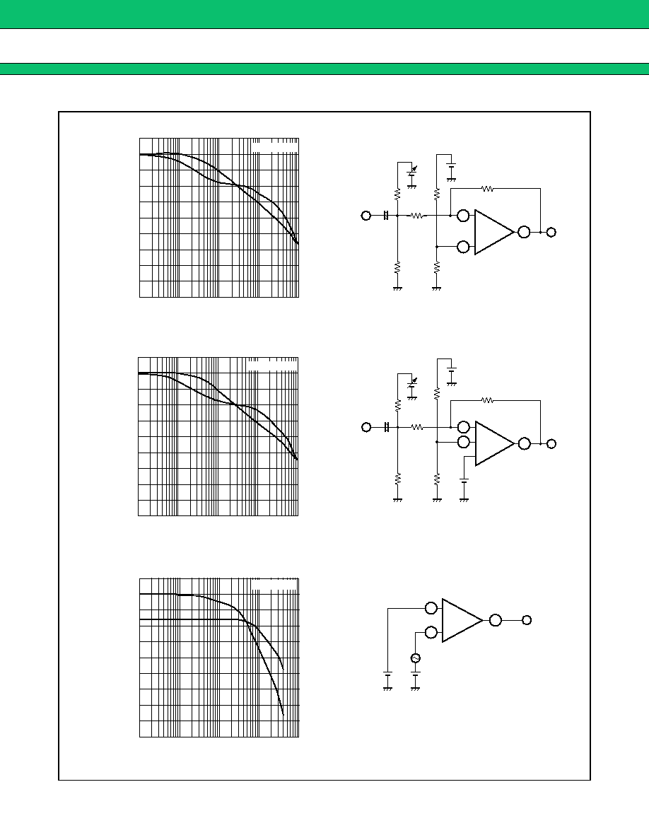
Error amplifier gain and phase vs. Frequency
Gain A
V
(dB)
Frequency f (Hz)
Phase
(deg)
Current detection amplifier gain and phase vs. Frequency
Gain A
V
(dB)
Frequency f (Hz)
Phase
(deg)
Error amplifier gain and phase vs. Frequency
Gain A
V
(dB)
Frequency f (Hz)
Phase
(deg)
MB3887
15
(Continued)
800
700
600
500
400
300
200
100
0
740
-
40
-
20
0
20
40
60
80
100
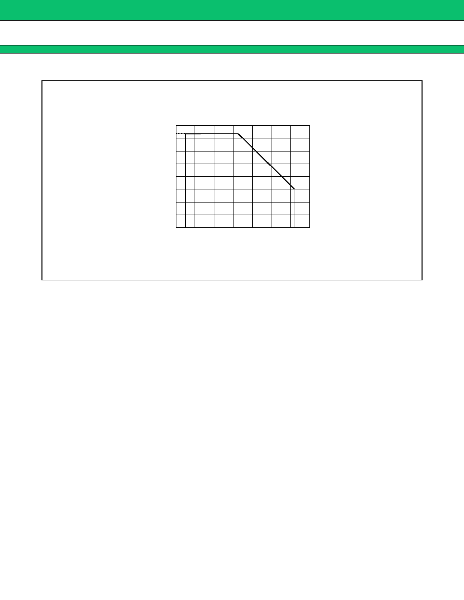
Power dissipation vs. Operating ambient temperature
Power dissipation P
D
(mW)
Operating ambient temperature Ta (
∞
C)

MB3887
16
FUNCTIONAL DESCRIPTION
1.
DC/DC Converter Unit
(1) Reference voltage block (REF)
The reference voltage generator uses the voltage supplied from the VCC terminal (pin 18) to generate a tem-
perature-compensated, stable voltage (5.0 V Typ) used as the reference supply voltage for the IC's internal
circuitry.
This terminal can also be used to obtain a load current to a maximum of 1mA from the reference voltage VREF
terminal (pin 6) .
(2) Triangular wave oscillator block (OSC)
The triangular wave oscillator builds the capacitor for frequency setting into, and generates the triangular wave
oscillation waveform by connecting the frequency setting resistor with the RT terminal (pin 17) .
The triangular wave is input to the PWM comparator on the IC.
(3) Error amplifier block (Error Amp1)
This amplifier detects the output signal from the current detection amplifier (Current amp1) , compares this to
the
+
INE1 terminal (pin 9) , and outputs a PWM control signal to be used in controlling the charging current.
In addition, an arbitrary loop gain can be set up by connecting a feedback resistor and capacitor between the
FB1 terminal (pin 7) and -INE1 terminal (pin 8) , providing stable phase compensation to the system.
(4) Error amplifier block (Error Amp2)
This amplifier (Error Amp2) detects voltage drop of the AC adapter and outputs a PWM control signal.
In addition, an arbitrary loop gain can be set by connecting a feedback resistor and capacitor from the FB2
terminal (pin 5) to the
-
INE2 terminal (pin 4) of the error amplifier, enabling stable phase compensation to the
system.
(5) Error amplifier block (Error Amp3)
This error amplifier (Error Amp3) detects the output voltage from the DC/DC converter and outputs the PWM
control signal. External output voltage setting resistors can be connected to the error amplifier inverted input
terminal to set the desired level of output voltage from 1 cell to 4 cells.
In addition, an arbitrary loop gain can be set by connecting a feedback resistor and capacitor from the FB3
terminal (pin 15) to the
-
INE3 terminal (pin 16) of the error amplifier, enabling stable phase compensation to
the system.
Connecting a soft-start capacitor to the CS terminal (pin 22) prevents rush currents when the IC is turned on.
Using an error amplifier for soft-start detection makes the soft-start time constant, independent of the output load.
(6) Current detection amplifier block (Current Amp1)
The current detection amplifier (Current Amp1) detects a voltage drop which occurs between both ends of the
output sense resistor (R
S
) due to the flow of the charge current, using the
+
INC1 terminal (pin 13) and
-
INC1
terminal (pin 12) . Then it outputs the signal amplified by 20 times to the error amplifier (Error Amp1) at the next
stage.

MB3887
17
(7) PWM comparator block (PWM Comp.)
The PWM comparator circuit is a voltage-pulse width converter for controlling the output duty of the error
amplifiers (Error Amp1 to Error Amp3) depending on their output voltage.
The PWM comparator circuit compares the triangular wave generated by the triangular wave oscillator to the
error amplifier output voltage and turns on the external output transistor during the interval in which the triangular
wave voltage is lower than the error amplifier output voltage.
(8) Output block (OUT)
The output circuit uses a totem-pole configuration capable of driving an external P-channel MOS FET.
The output "L" level sets the output amplitude to 6 V (Typ) using the voltage generated by the bias voltage block
(VH) .
This results in increasing conversion efficiency and suppressing the withstand voltage of the connected external
transistor in a wide range of input voltages.
(9) Control block (CTL)
Setting the CTL terminal (pin 14) low places the IC in the standby mode. (The supply current is 10
µ
A at maximum
in the standby mode.)
CTL function table
(10) Bias voltage block (VH)
The bias voltage circuit outputs V
CC
-
6 V (Typ) as the minimum potential of the output circuit. In the standby
mode, this circuit outputs the potential equal to VCC.
2.
Protection Functions
Under voltage lockout protection circuit (UVLO)
The transient state or a momentary decrease in supply voltage or internal reference voltage (VREF) , which
occurs when the power supply (VCC) is turned on, may cause malfunctions in the control IC, resulting in
breakdown or degradation of the system.
To prevent such malfunction, the under voltage lockout protection circuit detects a supply voltage or internal
reference voltage drop and fixes the OUT terminal (pin 20) to the "H" level. The system restores voltage supply
when the supply voltage or internal reference voltage reaches the threshold voltage of the under voltage lockout
protection circuit.
Protection circuit (UVLO) operation function table
When UVLO is operating (VCC or VREF voltage is lower than UVLO threshold voltage.)
CTL
Power
OUTD
L
OFF (Standby)
Hi-Z
H
ON (Active)
L
OUTD
OUT
CS
Hi-Z
H
L
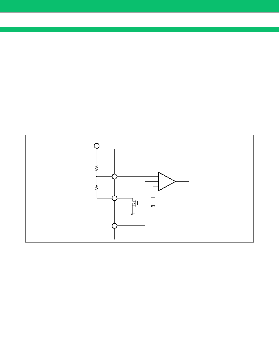
MB3887
18
3.
Soft-Start Function
Soft-start block (SOFT)
Connecting a capacitor to the CS terminal (pin 22) prevents rush currents when the IC is turned on. Using an
error amplifier for soft-start detection makes the soft-start time constant, being independent of the output load
of the DC/DC converter.
SETTING THE CHARGING VOLTAGE
The charging voltage (DC/DC output voltage) can be set by connecting external voltage setting resistors (R3,
R4) to the
-
INE3 terminal (pin 16) . Be sure to select a resistor value that allows you to ignore the on-resistor
(35
, 1mA) of the internal FET connected to the OUTD terminal (pin 11) . In standby mode, the charging
voltage is applied to OUTD termial. Therefore, output voltage must be adjusted so that voltage applied to OUTD
terminal is 17 V or less.
Battery charging voltage : V
O
V
O
(V)
=
(R3
+
R4)
/
R4
◊
4.2 (V)
METHOD OF SETTING THE CHARGING CURRENT
The charge current (output limit current) value can be set with the voltage at the
+
INE1 terminal (pin 9) .
If a current exceeding the set value attempts to flow, the charge voltage drops according to the set current value.
Battery charge current setting voltage :
+
INE1
+
INE1 (V)
=
20
◊
I1 (A)
◊
R
S
(
)
METHOD OF SETTING THE TRIANGULAR WAVE OSCILLATION FREQUENCY
The triangular wave oscillation frequency can be set by the timing resistor (R
T
) connected the RT terminal (pin 17) .
Triangular wave oscillation frequency : f
OSC
f
OSC
(kHz) := 13630
/
R
T
(k
)
<Error Amp3>
-
+
+
4.2 V
R3
V
O
R4
-
INE3
OUTD
CS
16
B
11
22
MB3887
19
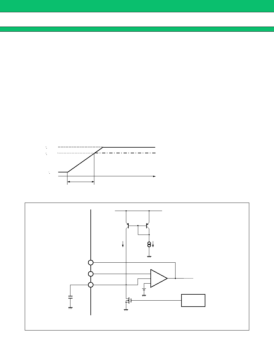
METHOD OF SETTING THE SOFT-START TIME
For preventing rush current upon activation of IC, the IC allows soft-start using the capacitor (Cs) connected to
the CS terminal (pin 22) .
When CTL terminal (pin 14) is placed under "H" level and IC is activated (V
CC
UVLO threshold voltage) , Q2
is turned off and the external soft-start capacitor (Cs) connected to the CS terminal is charged at 10
µ
A.
Error Amp output (FB3 terminal (pin 15) ) is determined by comparison between the lower voltage of the two
non-reverse input terminals (4.2 V and CS terminal voltage) and reverse input terminal voltage (
-
INE3 terminal
(pin 16) voltage) . Within the soft-start period (CS terminal voltage
<
4.2 V) , FB3 is determined by comparison
between
-
INE3 terminal voltage and CS terminal voltage, and DC/DC converter output voltage goes up propor-
tionately with the increase of CS terminal voltage caused by charging on the soft-start capacitor.Soft-start time
is found by the following formula :
Soft-start time : ts (time to output 100
%
)
t
S
(s) := 0.42
◊
C
S
(
µ
F)
=
4.9 V
=
4.2 V
=
0 V
CS terminal voltage
Comparison with Error Amp block
-
INE3
voltage.
Soft-start time: ts
15
16
22
-
+
+
UVLO
VREF
10
µ
A
10
µ
A
Q2
4.2 V
Error
Amp3
FB3
-
INE3
CS
C
S
Soft-start circuit
MB3887
20
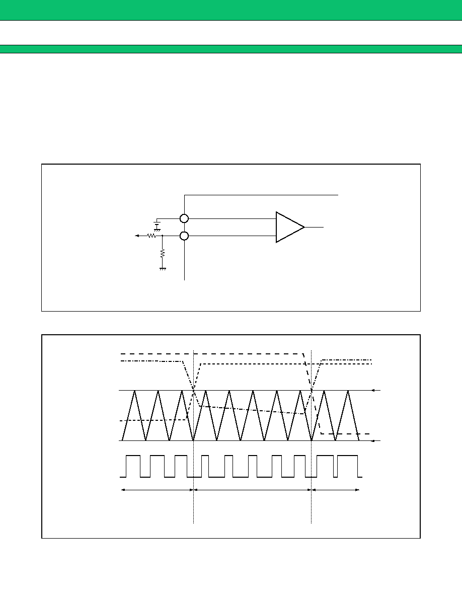
AC ADAPTOR VOLTAGE DETECTION
With an external resistor connected to the
+
INE2 terminal (pin 3) , the IC enters the dynamically-controlled
charging mode to reduce the charge current to keep AC adapter power constant when the partial potential point
A of the AC adapter voltage (VCC) becomes lower than the voltage at the
-
INE2 terminal.
AC adapter detection voltage setting : Vth
Vth (V)
=
(R1
+
R2)
/
R2
◊
-
INE2
OPERATION TIMING DIAGRAM
-
+
VCC
R1
R2
+
INE2
-
INE2
A
<Error Amp2>
4
3
2.5 V
1.5 V
Error Amp2 FB2
Error Amp1 FB1
Error Amp2 FB3
OUT
Constant voltage control
Constant current control
AC adapter dynamically-
controlled charging
MB3887
21
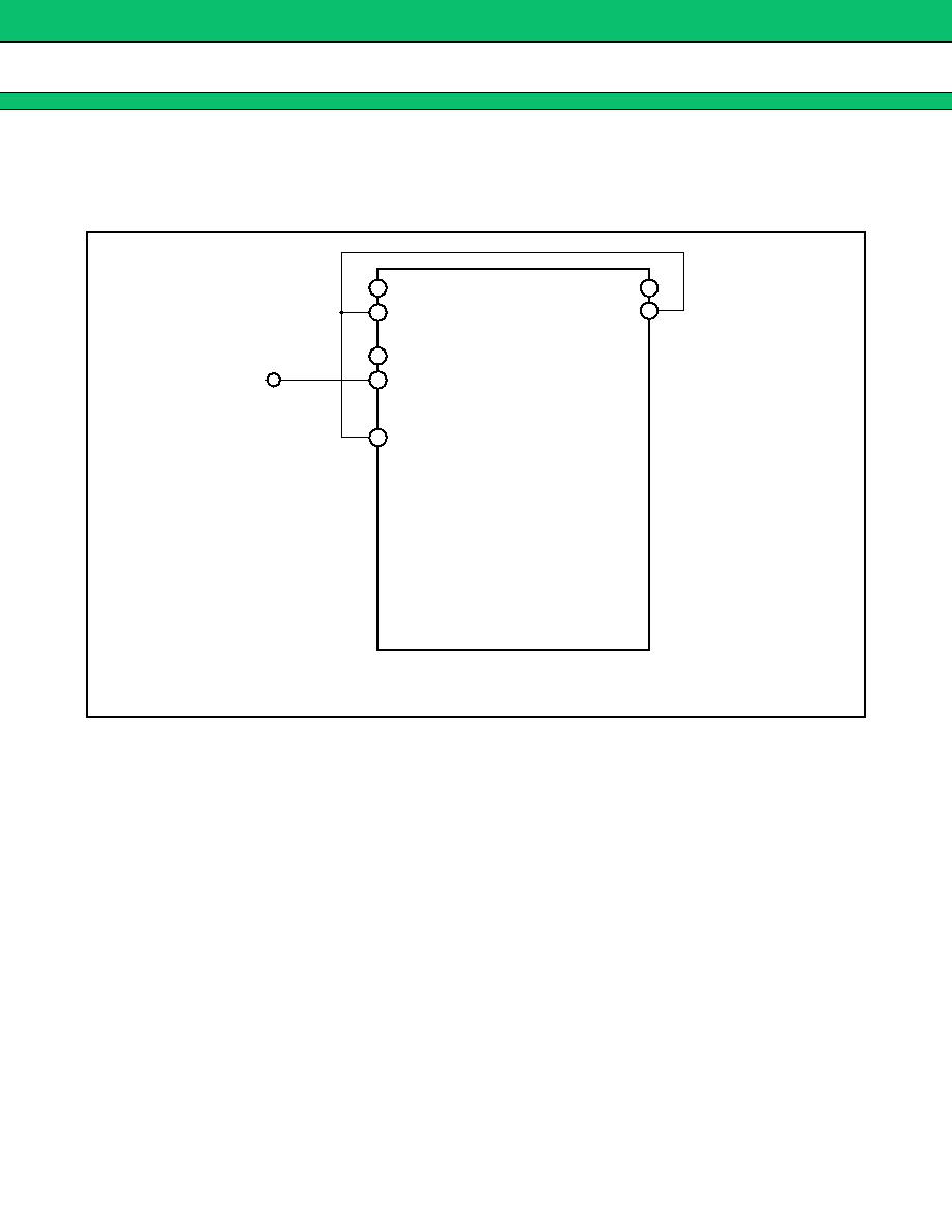
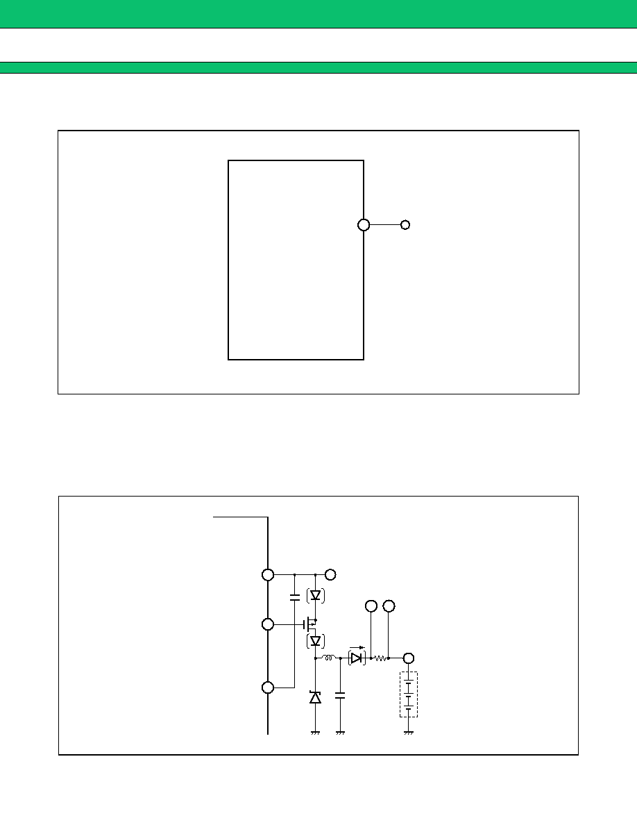
PROCESSING WITHOUT USING THE CURRENT AMP
When Current Amp is not used, connect the
+
INC1 terminal (pin 13) ,
+
INC2 terminal (pin 24) ,
-
INC1 terminal
(pin 12) , and
-
INC2 terminal (pin 1) to VREF, and then leave OUTC1 terminal (pin 10) and OUTC2 terminal
(pin 2) open.
24
13
12
1
2
10
6
-
INC1
+
INC1
+
INC2
-
INC2
OUTC1
OUTC2
VREF
"Open"
Connection when Current Amp is not used
MB3887
22
PROCESSING WITHOUT USING OF THE ERROR AMP
When Error Amp is not used, leave FB1 terminal (pin 7) , FB2 terminal (pin 5) open and connect the
-
INE1
terminal (pin 8) and
-
INE2 terminal (pin 4) to GND and connect
+
INE1 terminal (pin 9) , and
+
INE2 terminal (pin
3) , to VREF.
9
5
8
4
7
+
INE1
GND
+
INE2
-
INE1
-
INE2
VREF
FB2
FB1
23
6
3
"Open"
Connection when Error Amp is not used
MB3887
23
PROCESSING WITHOUT USING OF THE CS TERMINAL
When soft-start function is not used, leave the CS terminal (pin 22) open.
NOTE ON AN EXTERNAL REVERSE-CURRENT PREVENTIVE DIODE
∑ Insert a reverse-current preventive diode at one of the three locations marked * to prevent reverse current from
the battery.
∑ When selecting the reverse current prevention diode, be sure to consider the reverse voltage (V
R
) and reverse
current (I
R
) of the diode.
22
CS
"Open"
Connection when soft-start time is not specified
VCC(O)
OUT
VIN
VH
I1
R
S
BATT
Battery
A
B
*
*
*
21
20
19

MB3887
24
THE SEQUENCE OF THE START-UP AND OFF OF THE POWER SUPPLY
Please start up and off the VCC terminal (pin 18) and VCC(O) terminal (pin 21) of the power supply terminal at
the same time. No do occurrence of the bias from the VH terminal (pin 19) , when there is a period of 8 V or
less in the VCC voltage after previously starting up VCC(O). At this time, there is a possibility of leading to
permanent destruction of the device when the voltage of 17 V or more is impressed to the VCC(O) terminal.
Moreover, when earliness VCC falls more than VCC(O) when falling, it is similar.
MB3887
25
APPLICATION EXAMPLE
A
B
Q1
Output voltage (Battery
voltage) is adjustable
D1
I1
Battery
R8 100 k
C10
5600 pF
+
+
+
R9
10 k
R14 1 k
R10 30 k
R11 30 k
R7
22 k
R18
200 k
R19
100 k
R17
100 k
C6
1500 pF
C4
0.022
µ
F
R3
330 k
R2
47 k
C9 0.1
µ
F
C7 0.1
µ
F
C5
0.1
µ
F
C2
100
µ
F
C3 100
µ
F
C1 22
µ
F
0.033
R1
22
µ
H
L1
R4 82 k
R5 330 k
R6 68 k
R15
120
R16
2
00 k
Q2
SW
R12
30 k
R13
20 k
C8
10000 pF
A
B
AC Adapto
r
IIN
V
O
+
-
-
+
8
10
13
12
9
+
-
-
+
4
2
24
1
3
◊
20
◊
20
+ + + -
5
20
21
19
-
+
+
+
-
11
16
22
17
6
23
14
18
<Current Amp1>
7
VREF
<Current Amp2>
VREF
VREF
VREF
VREF
5.0 V
4.2 V
10
µ
A
15
<SOFT>
2.5 V
1.5 V
<OUT>
<OSC>
Bias
Voltage
<VH>
<REF>
<CTL>
<PWM Comp.>
Drive
VCC
(V
CC
-
6 V)
(VCC UVLO)
VCC
VCC
CTL
215 k
35 k
0.91 V
(0.77 V)
VREF
UVLO
4.2 V
bias
-
INC2
OUTD
FB2
OUTC2
VREF
-
INE2
+
INE2
+
INE1
FB1
OUTC1
-
INE1
-
INC1
+
INC2
GND
CS
VCC (O)
OUT
VH
RT
-
INE3
FB3
+
INC1
45 pF
<Error Amp1>
<Error Amp2>
<Error Amp3>
<UVLO>
VCC
VIN
=
13.93 V to 25 V
(at 3 cell)
VIN
=
17.65 V to 25 V
(at 4 cell)
Note:
Set output voltage so
that voltage applied to
OUTD terminal is 17 V or
less.

MB3887
26
PARTS LIST
Note : VISHAY SILICONIX : VISHAY Intertechnology, Inc.
ROHM : ROHM CO., LTD.
TDK : TDK Corporation
SANYO : SANYO Electric Co., Ltd.
KYOCERA : Kyocera Corporation
MURATA : Murata Manufacturing Co., Ltd.
SEIDEN TECHNO : SEIDEN TECHNO CO., LTD.
KOA : KOA Corporation
ssm : SUSUMU Co., Ltd.
OS-CON is a trademark of SANYO Electric Co., Ltd.
COMPONENT
ITEM
SPECIFICATION
VENDOR
PARTS No.
Q1
Q2
P-ch FET
N-ch FET
VDS
=
-
30 V, ID
=
±
8 A (Max)
VDS
=
60 V, ID
=
0.115 A
(Max)
VISHAY SILICONIX
VISHAY SILICONIX
Si4435DY
2N7002E
D1
Diode
VF
=
0.42 V (Max) , IF
=
3 A
ROHM
RB053L-30
L1
Inductor
22
µ
H
3.5 A,
31.6 m
TDK
SLF12565T-
220M3R5
C1
C2, C3
C4
C5
C6
C7
C8
C9
C10
OS-CON
TM
Electrolytic Condenser
Ceramics Condenser
Ceramics Condenser
Ceramics Condenser
Ceramics Condenser
Ceramics Condenser
Ceramics Condenser
Ceramics Condenser
22
µ
F
100
µ
F
0.022
µ
F
0.1
µ
F
1500 pF
0.1
µ
F
10000 pF
0.1
µ
F
5600 pF
25 V (10
%
)
25 V (10
%
)
50 V
16 V
10 V
25 V
10 V
16 V
10 V
SANYO
SANYO
TDK
KYOCERA
MURATA
MURATA
MURATA
KYOCERA
MURATA
25SL22M
25CV100AX
C1608JB1H223K
CM21W5R104K16
GRM39B152K10
GRM39F104KZ25
GRM39B103K10
CM21W5R104K16
GRM39B562K10
R1
R2
R3
R4
R5
R6
R7
R8
R9
R10 to R12
R13
R14
R15
R16, R18
R17, R19
Resistor
Resistor
Resistor
Resistor
Resistor
Resistor
Resistor
Resistor
Resistor
Resistor
Resistor
Resistor
Resistor
Resistor
Resistor
0.033
47 k
330 k
82 k
330 k
68 k
22 k
100 k
10 k
30 k
20 k
1 k
120
200 k
100 k
1.0
%
0.5
%
0.5
%
0.5
%
0.5
%
0.5
%
0.5
%
0.5
%
1.0
%
0.5
%
0.5
%
0.5
%
0.5
%
0.5
%
0.5
%
SEIDEN TECHNO
KOA
KOA
KOA
KOA
KOA
KOA
KOA
KYOCERA
KOA
KOA
KOA
ssm
KOA
KOA
RK73Z1J-0D
RK73G1J-473D
RK73G1J-334D
RK73G1J-823D
RK73G1J-334D
RK73G1J-683D
RK73G1J-223D
RK73G1J-104D
CR21-103-F
RK73G1J-303D
RK73G1J-203D
RK73G1J-102D
RR0816P121D
RK73G1J-204D
RK73G1J-104D
MB3887
27
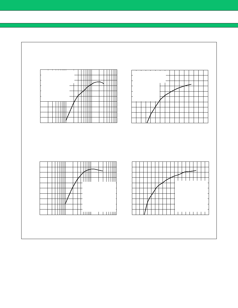
REFERENCE DATA
(Continued)
100
98
96
94
92
90
88
86
84
82
80
10 m
100 m
1
10
Ta
=
+
25
∞
C
VIN
=
19 V
BATT charge voltage
=
set at 12.6 V
SW
=
ON
Efficiency
(%)
=
(V
BATT
◊
I
BATT
) /
(V
IN
◊
I
IN
)
◊
100
100
98
96
94
92
90
88
86
84
82
80
0
2
4
6
8
10
12
14
16
Ta
= +
25
∞
C
VIN
=
19 V
BATT charge voltage
=
set at 12.6 V
SW
=
ON
Efficiency
(%)
=
(V
BATT
◊
I
BATT
) /
(V
IN
◊
I
IN
)
◊
100
100
98
96
94
92
90
88
86
84
82
80
10 m
100 m
1
10
Ta
= +
25
∞
C
VIN
=
19 V
BATT charge voltage
=
set at 16.8 V
SW
=
ON
Efficiency
(%)
=
(V
BATT
◊
I
BATT
) /
(V
IN
◊
I
IN
)
◊
100
100
98
96
94
92
90
88
86
84
82
80
0
2
4
6
8
10
12
14
16
18
20
Ta
= +
25
∞
C
VIN
=
19 V
BATT charge voltage
=
set at 16.8 V
SW
=
ON
Efficiency
(%)
=
(V
BATT
◊
I
BATT
) /
(V
IN
◊
I
IN
)
◊
100
Conversion efficiency vs. Charge current
(Constant voltage mode)
Conversion efficiency vs. Charge current
(Constant current mode)
Conversion efficiency
(
%
)
BATT charge current I
BATT
(A)
Conversion efficiency
(
%
)
BATT charge voltage V
BATT
(V)
Conversion efficiency vs. Charge current
(Constant voltage mode)
Conversion efficiency vs. Charge current
(Constant current mode)
Conversion efficiency
(
%
)
BATT charge current I
BATT
(A)
Conversion efficiency
(
%
)
BATT charge voltage V
BATT
(V)
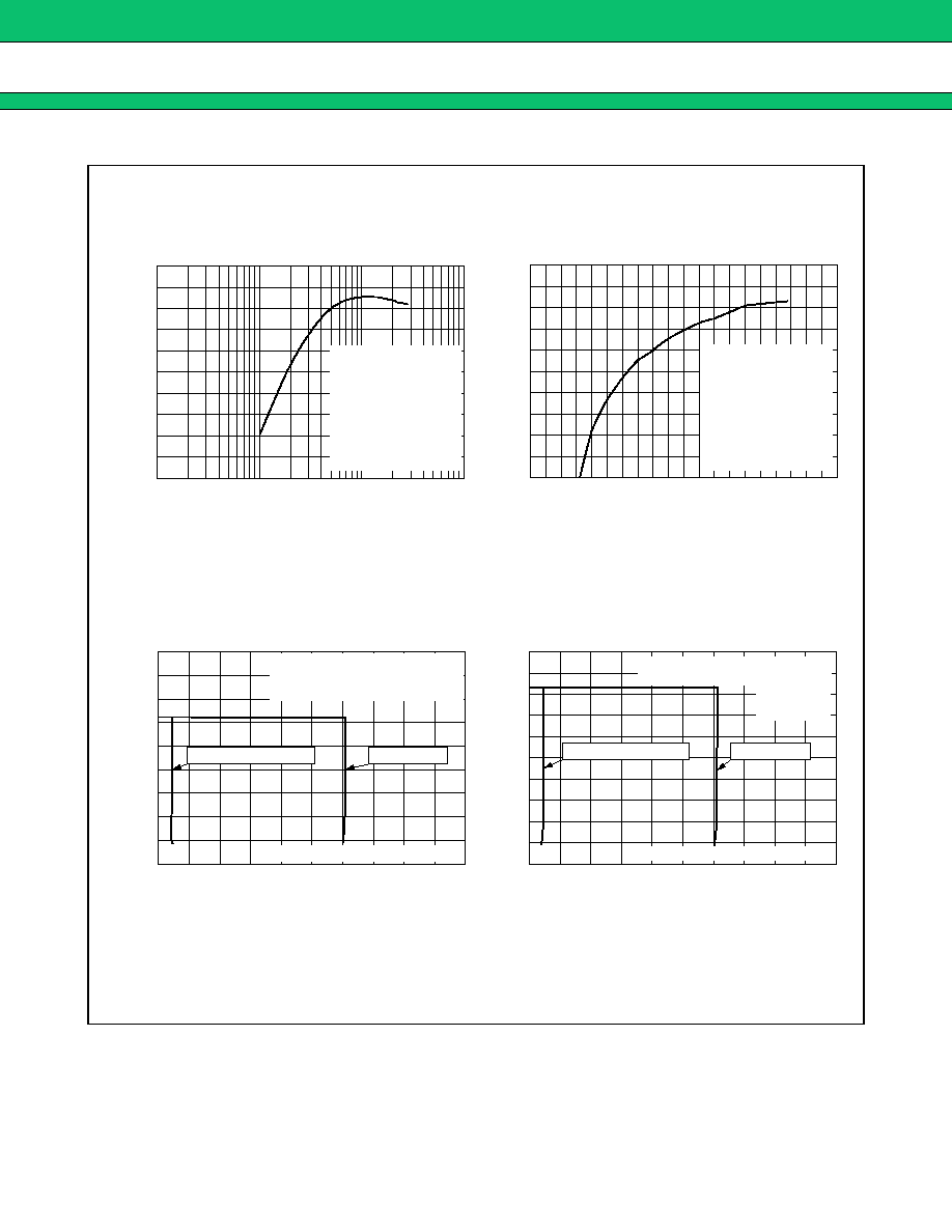
MB3887
28
(Continued)
100
98
96
94
92
90
88
86
84
82
80
10 m
100 m
1
10
Ta
= +
25
∞
C
VIN
=
19 V
BATT charge voltage
=
set at 16.8 V
SW
=
ON
Efficiency
(%)
=
(V
BATT
◊
I
BATT
) /
(V
IN
◊
I
IN
)
◊
100
100
98
96
94
92
90
88
86
84
82
80
0
2
4
6
8
10
12
14
16
18
20
Ta
= +
25
∞
C
VIN
=
19 V
BATT charge voltage
=
set at 16.8 V
SW
=
ON
Efficiency
(%)
=
(V
BATT
◊
I
BATT
) /
(V
IN
◊
I
IN
)
◊
100
Conversion efficiency vs. Charge current
(Constant voltage mode)
Conversion efficiency vs. Charge current
(Constant current mode)
Conversion efficiency
(
%
)
BATT charge current I
BATT
(A)
Conversion efficiency
(
%
)
BATT charge voltage V
BATT
(V)
18
16
14
12
10
8
6
4
2
0
0
1
2
3
2.5
1.5
0.5
4
5
4.5
3.5
Dead Battery MODE
DCC MODE
DCC
:
Dynamically-Controlled
Ta
= +
25
∞
C VIN
=
19 V
BATT
:
Electronic load
,
(Product of KIKUSUI PLZ-150W)
20
18
16
14
12
10
8
6
4
2
0
0
0.5
1
1.5
2
2.5
3
3.5
4
4.5
5
Dead Battery MODE
DCC MODE
DCC : Dynamically-Controlled
BATT
:
Electronic load
,
(Product of KIKUSUI PLZ-150W)
Ta
= +
25
∞
C
VIN
=
19 V
BATT voltage vs. BATT charge current
(set at 12.6 V)
BATT voltage V
BATT
(V
)
BATT charge current I
BATT
(A)
BATT voltage vs. BATT charge current
(set at 16.8 V)
BATT voltage V
BATT
(V
)
BATT charge current I
BATT
(A)
MB3887
29
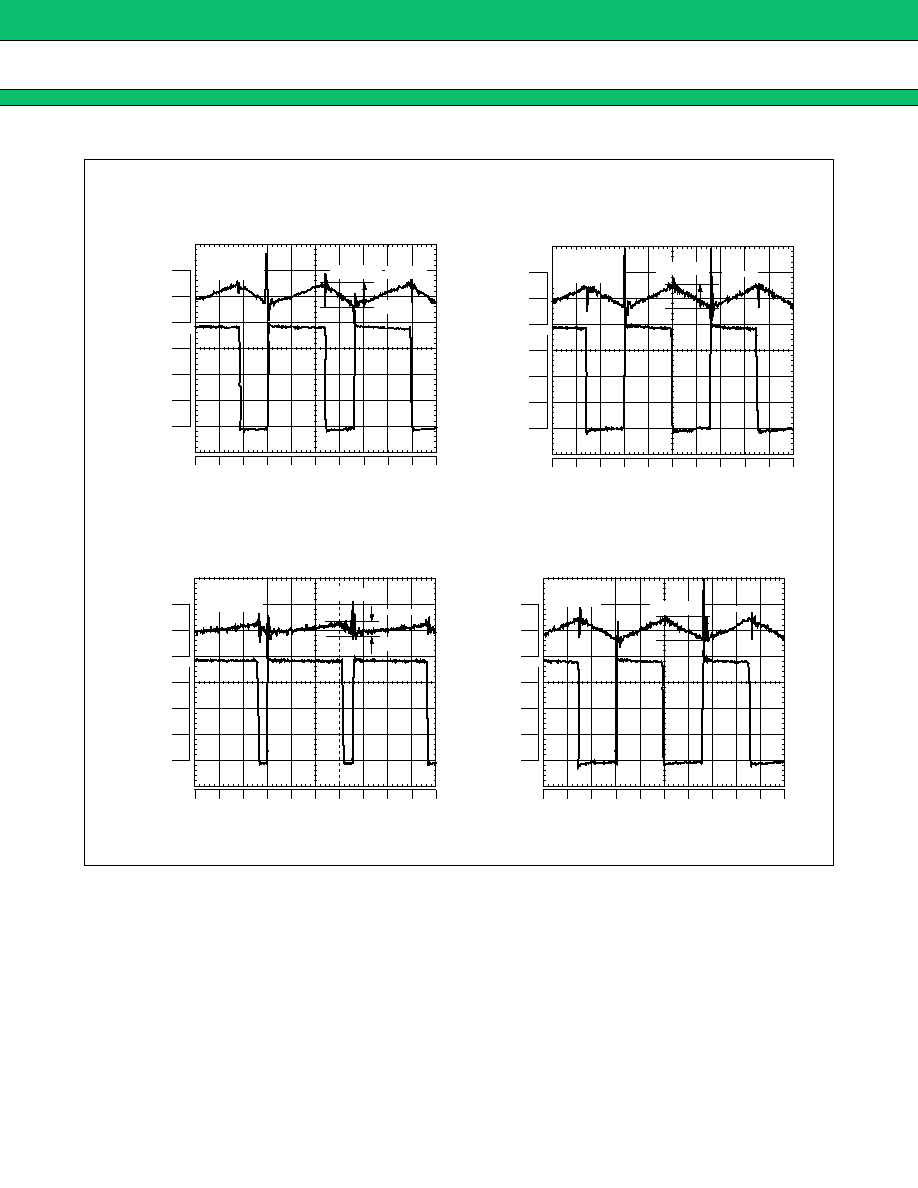
(Continued)
100
0
-
100
15
10
5
0
V
BATT
(mV)
V
D
(V)
Ta
= +
25
∞
C
VIN
=
19 V
BATT
=
1.5 A
98 mVp-p
0
1
2
3
4
5
6
7
8
9
10
(
µ
s)
V
D
V
BATT
100
0
-
100
15
10
5
0
V
BATT
(mV)
V
D
(V)
Ta
= +
25
∞
C
VIN
=
19 V
BATT
=
3.0 A
98 mVp-p
V
D
V
BATT
0
1
2
3
4
5
6
7
8
9
10
(
µ
s)
100
0
-
100
15
10
5
0
V
BATT (
mV)
V
D
(V)
Ta
= +
25
∞
C
VIN
=
19 V
BATT
=
1.5 A
58 mVp-p
V
BATT
0
1
2
3
4
5
6
7
8
9
10
(
µ
s)
V
D
100
0
-
100
15
10
5
0
V
BATT
(mV)
V
D
(V)
96 mVp-p
V
D
V
BATT
0
1
2
3
4
5
6
7
8
9
10
(
µ
s)
VIN
=
19 V
BATT
=
3.0 A
Ta
= +
25
∞
C
Switching waveform constant voltage mode
(set at 12.6 V)
Switching waveform constant current mode
(set at 12.6 V, with 10 V)
Switching waveform constant voltage mode
(set at 16.8 V)
Switching waveform constant current mode
(set at 16.8 V, with 10 V)
MB3887
30
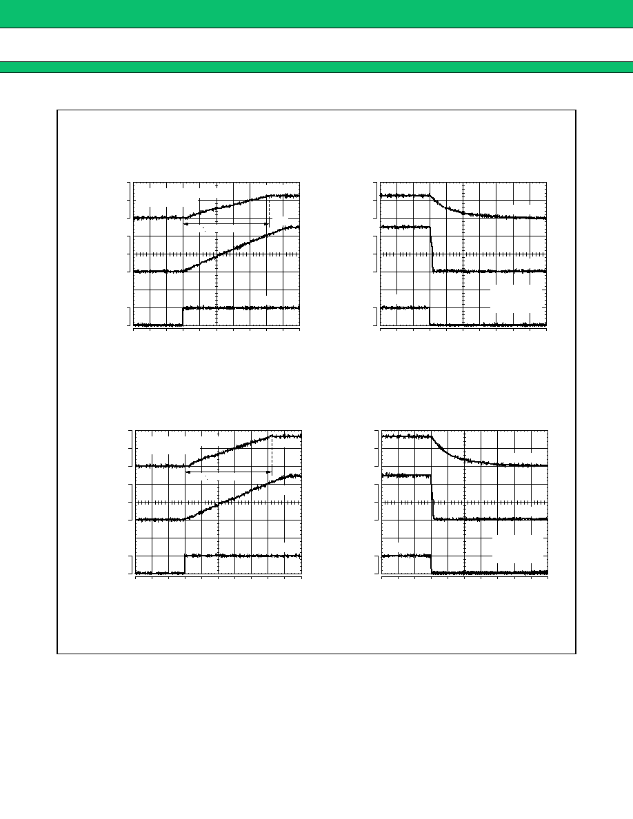
(Continued)
20
10
0
4
2
0
5
0
V
CTL
(V)
V
CS
(V)
V
BATT
(V)
0
2
4
6
8
10 12 14 16 18 20
(ms)
Ta
= +
25
∞
C, VIN
=
19 V
BATT
=
12
V
BATT
V
CTL
ts
=
10.4 ms
V
CS
20
10
0
4
2
0
5
0
V
CTL
(V)
V
CS
(V)
V
BATT
(V)
0
2
4
6
8
10 12 14 16 18 20
(ms)
Ta
= +
25
∞
C
VIN
=
19 V
BATT
=
12
V
BATT
V
CTL
V
CS
20
10
0
4
2
0
5
0
V
CTL
(V)
V
CS
(V)
V
BATT
(V)
0
2
4
6
8
10 12 14 16 18 20
(ms)
V
BATT
ts
=
10.4 ms
V
CS
V
CTL
Ta
= +
25
∞
C, VIN
=
19 V
BATT
=
12
20
10
0
4
2
0
5
0
V
CTL
(V)
V
CS
(V)
V
BATT
(V)
0
2
4
6
8
10 12 14 16 18 20
(ms)
Ta
= +
25
∞
C
VIN
=
19 V
BATT
=
12
V
BATT
V
CTL
V
CS
Soft-start operating waveform
constant voltage mode
(set at 12.6 V)
Discharge operating waveform
constant voltage mode
(set at 12.6 V)
Soft-start operating waveform
constant voltage mode
(set at 16.8 V)
Discharge operating waveform
constant voltage mode
(set at 16.8 V)

MB3887
31
USAGE PRECAUTIONS
∑ Printed circuit board ground lines should be set up with consideration for common impedance.
∑ Take appropriate static electricity measures.
∑
Containers for semiconductor materials should have anti-static protection or be made of conductive material.
∑
After mounting, printed circuit boards should be stored and shipped in conductive bags or containers.
∑
Work platforms, tools, and instruments should be properly grounded.
∑
Working personnel should be grounded with resistance of 250 k
to 1 M
between body and ground.
∑ Do not apply negative voltages.
∑
The use of negative voltages below
-
0.3 V may create parasitic transistors on LSI lines, which can cause
malfunction.
ORDERING INFORMATION
Part number
Package
Remarks
MB3887PFV
24-pin plastic SSOP
(FPT-24P-M03)
MB3887
32
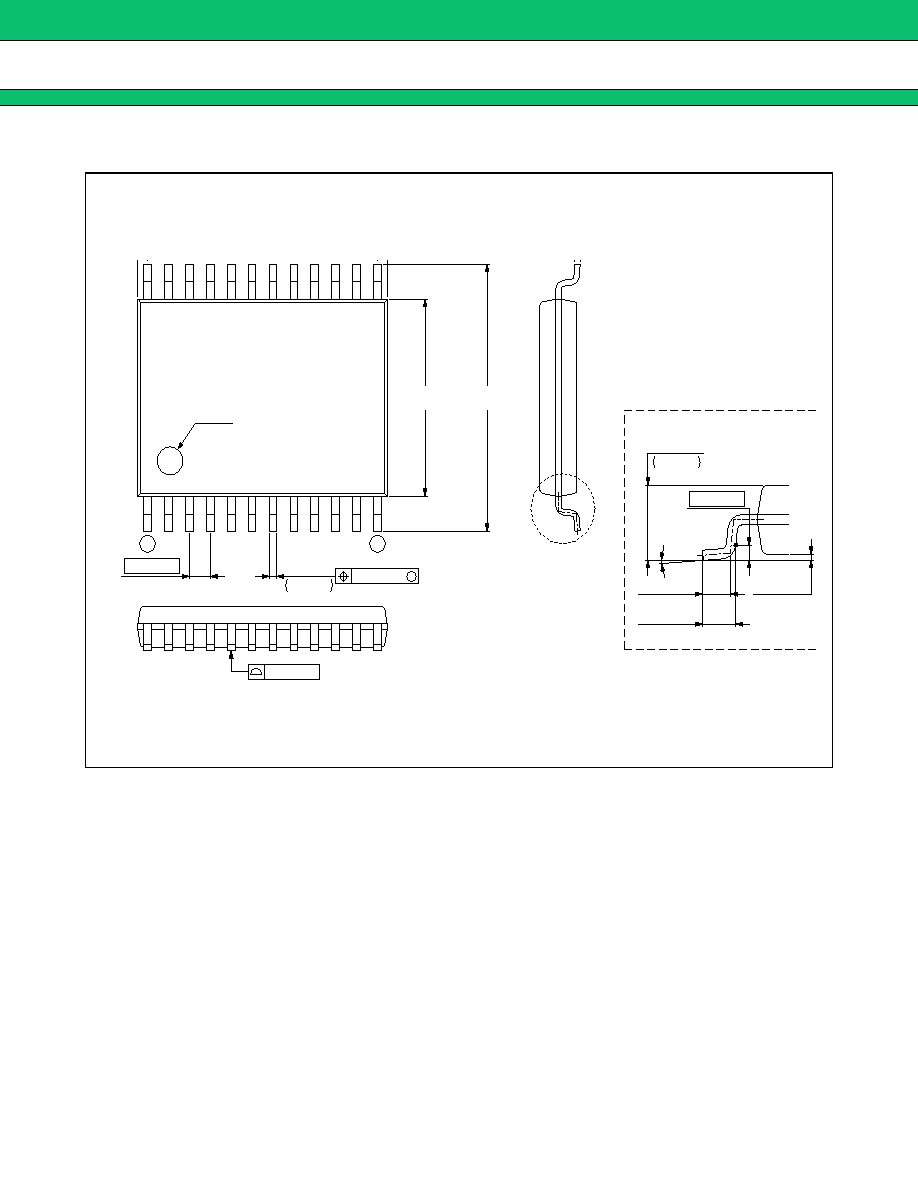
PACKAGE DIMENSION
24-pin plastic SSOP
(FPT-24P-M03)
Note 1) *1 : Resin protrusion. (Each side :
+
0.15 (.006) Max) .
Note 2) *2 : These dimensions do not include resin protrusion.
Note 3) Pins width and pins thickness include plating thickness.
Note 4) Pins width do not include tie bar cutting remainder.
Dimensions in mm (inches) .
Note : The values in parentheses are reference values.
2003 FUJITSU LIMITED F24018S-c-4-5
5.60±0.10
7.60±0.20
(.220±.004) (.299±.008)
*
2
0.10(.004)
1
12
0.65(.026)
≠0.07
+0.08
0.24
.009
+.003
≠.003
M
0.13(.005)
INDEX
"A"
0.25(.010)
0.10±0.10
(.004±.004)
(Stand off)
Details of "A" part
(Mounting height)
1.25
+0.20
≠0.10
≠.004
+.008
.049
0~8∞
0.50±0.20
(.020±.008)
0.60±0.15
(.024±.006)
0.10(.004)

MB3887
FUJITSU LIMITED
All Rights Reserved.
The contents of this document are subject to change without notice.
Customers are advised to consult with FUJITSU sales
representatives before ordering.
The information, such as descriptions of function and application
circuit examples, in this document are presented solely for the
purpose of reference to show examples of operations and uses of
Fujitsu semiconductor device; Fujitsu does not warrant proper
operation of the device with respect to use based on such
information. When you develop equipment incorporating the
device based on such information, you must assume any
responsibility arising out of such use of the information. Fujitsu
assumes no liability for any damages whatsoever arising out of
the use of the information.
Any information in this document, including descriptions of
function and schematic diagrams, shall not be construed as license
of the use or exercise of any intellectual property right, such as
patent right or copyright, or any other right of Fujitsu or any third
party or does Fujitsu warrant non-infringement of any third-party's
intellectual property right or other right by using such information.
Fujitsu assumes no liability for any infringement of the intellectual
property rights or other rights of third parties which would result
from the use of information contained herein.
The products described in this document are designed, developed
and manufactured as contemplated for general use, including
without limitation, ordinary industrial use, general office use,
personal use, and household use, but are not designed, developed
and manufactured as contemplated (1) for use accompanying fatal
risks or dangers that, unless extremely high safety is secured, could
have a serious effect to the public, and could lead directly to death,
personal injury, severe physical damage or other loss (i.e., nuclear
reaction control in nuclear facility, aircraft flight control, air traffic
control, mass transport control, medical life support system, missile
launch control in weapon system), or (2) for use requiring
extremely high reliability (i.e., submersible repeater and artificial
satellite).
Please note that Fujitsu will not be liable against you and/or any
third party for any claims or damages arising in connection with
above-mentioned uses of the products.
Any semiconductor devices have an inherent chance of failure. You
must protect against injury, damage or loss from such failures by
incorporating safety design measures into your facility and
equipment such as redundancy, fire protection, and prevention of
over-current levels and other abnormal operating conditions.
If any products described in this document represent goods or
technologies subject to certain restrictions on export under the
Foreign Exchange and Foreign Trade Law of Japan, the prior
authorization by Japanese government will be required for export
of those products from Japan.
F0501
©
2005 FUJITSU LIMITED Printed in Japan