DS04-27239-1E
FUJITSU SEMICONDUCTOR
DATA SHEET
ASSP For Power Supply Applications
(General-Purpose DC/DC Converter)
3-ch DC/DC Converter IC
MB39A112
s
DESCRIPTION
The MB39A112 is a 3-channel DC/DC converter IC using pulse width modulation (PWM) , and the MB39A112 is
suitable for down-conversion.
3-channel is built in TSSOP-20P package. Each channel can be controlled and soft-start.
The MB39A112 contains a constant voltage bias circuit for output block, capable of implementing an efficient
high-frequency DC/DC converter. It is ideal for built-in power supply such as ADSL modems.
s
REATURES
∑ Supports for down-conversion (CH1 to CH3)
∑ Power supply voltage range
: 7 V to 25 V
∑ Error amplifier threshold voltage : 1.00 V
±
1
%
(CH1)
: 1.23 V
±
1
%
(CH2, CH3)
∑ Oscillation frequency range
: 250 kHz to 2.6 MHz
∑ Built-in soft-start circuit independent of loads
∑ Built-in timer-latch short-circuit protection circuit
∑ Built-in totem-pole type output for P-channel MOS FET devices
∑ Built-in constant voltage (VCCO
-
5 V) bias circuit for output block
s
PACKAGE
20-pin plastic TSSOP
(FPT-20P-M06)
MB39A112
2
s
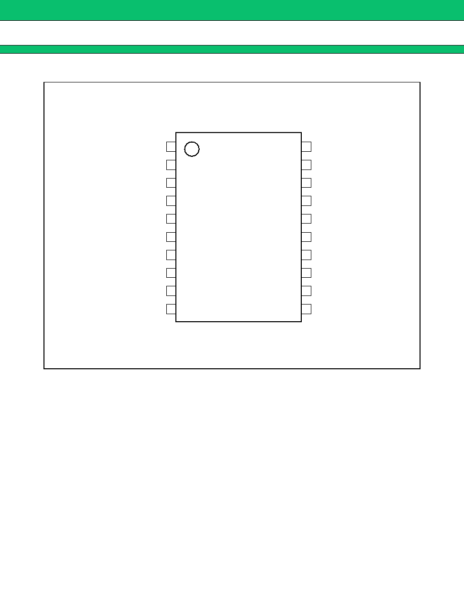
PIN ASSIGNMENT
(TOP VIEW)
(FPT-20P-M06)
CS1 : 1
-
INE1 : 2
FB1 : 3
VCC : 4
RT : 5
CT : 6
GND : 7
FB2 : 8
-
INE2 : 9
CS2 : 10
20 : VCCO
19 : OUT1
18 : OUT2
17 : OUT3
16 : VH
15 : GNDO
14 : CSCP
13 : FB3
12 :
-
INE3
11 : CS3
MB39A112
3
s
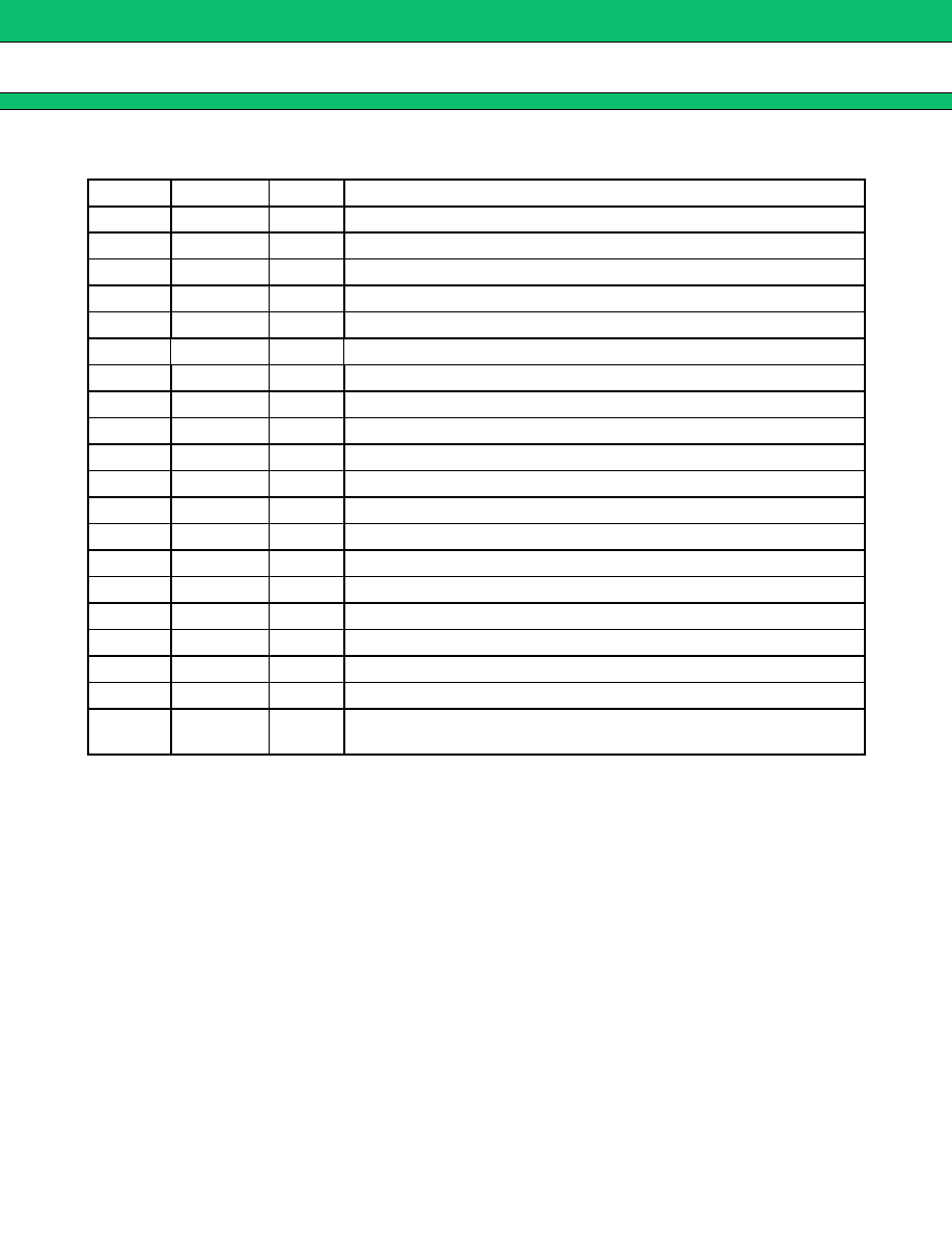
PIN DESCRIPTION
Pin No.
Symbol
I/O
Descriptions
1
CS1
CH1 soft-start setting capacitor connection terminal.
2
-
INE1
I
CH1 error amplifer inverted input terminal.
3
FB1
O
CH1 error amplifer output terminal.
4
VCC
Control circuit power supply terminal.
5
RT
Triangular-wave oscillation frequency setting resistor connection terminal.
6
CT
Triangular-wave oscillation frequency setting capacitor connection terminal.
7
GND
Ground terminal.
8
FB2
O
CH2 error amplifier output terminal.
9
-
INE2
I
CH2 error amplifier inverted input terminal.
10
CS2
CH2 soft-start setting capacitor connection terminal.
11
CS3
CH3 soft-start setting capacitor connection terminal.
12
-
INE3
I
CH3 error amplifier inverted input terminal.
13
FB3
O
CH3 error amplifier output terminal.
14
CSCP
Timer-latch short-circuit protection capacitor connection terminal.
15
GNDO
Ground terminal.
16
VH
O
Power supply terminal for driving output circuit. (VH
=
VCCO
-
5 V) .
17
OUT3
O
CH3 external Pch MOS FET gate driving terminal.
18
OUT2
O
CH2 external Pch MOS FET gate driving terminal.
19
OUT1
O
CH1 external Pch MOS FET gate driving terminal.
20
VCCO
Power supply terminal for driving output circuit. (Connect to same potential
as VCC terminal).
MB39A112
4
s
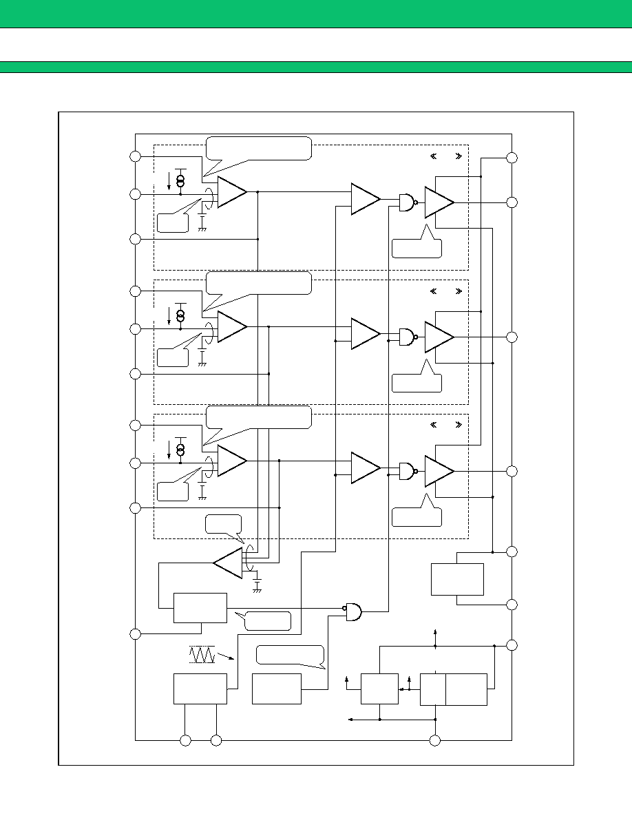
BLOCK DIAGRAM
-
+
+
+
-
2
1
3
19
-
+
+
+
-
9
10
8
18
-
+
+
-
+
+
+
+
-
12
11
13
14
5
6
7
17
16
15
4
20
-
INE1
CS1
FB1
-
INE2
CS2
FB2
-
INE3
CS3
FB3
CSCP
RT
CT
GND
OUT1
OUT2
OUT3
VH
GNDO
VCC
VCCO
VREF
Error
Amp1
1.0 V
10
µ
A
VREF
Error
Amp2
1.23 V
10
µ
A
VREF
SCP
OSC
UVLO
VREF
VR
Power
ON/OFF
CTL
Bias
Voltage
VH
I
O
=
150 mA
Pch
Drive3
VCCO
-
5 V
GND
bias
3.5 V
Error
Amp3
PWM
Comp.3
SCP
Comp.
1.23 V
2.7 V
2.5 V
2.0 V
10
µ
A
CH3
I
O
=
150 mA
Pch
Drive2
PWM
Comp.2
CH2
I
O
=
150 mA
Pch
Drive1
PWM
Comp.1
CH1
Threshold voltage
1.0 V
±
1
%
Threshold voltage
1.23 V
±
1
%
Threshold voltage
1.23 V
±
1
%
L
priority
L
priority
H
priority
H: at SCP
H: UVLO release
Error Amp Power Supply
SCP Comp. Power Supply
ErrorAmp Reference
1.0 V/1.23 V
L
priority
MB39A112
5
s
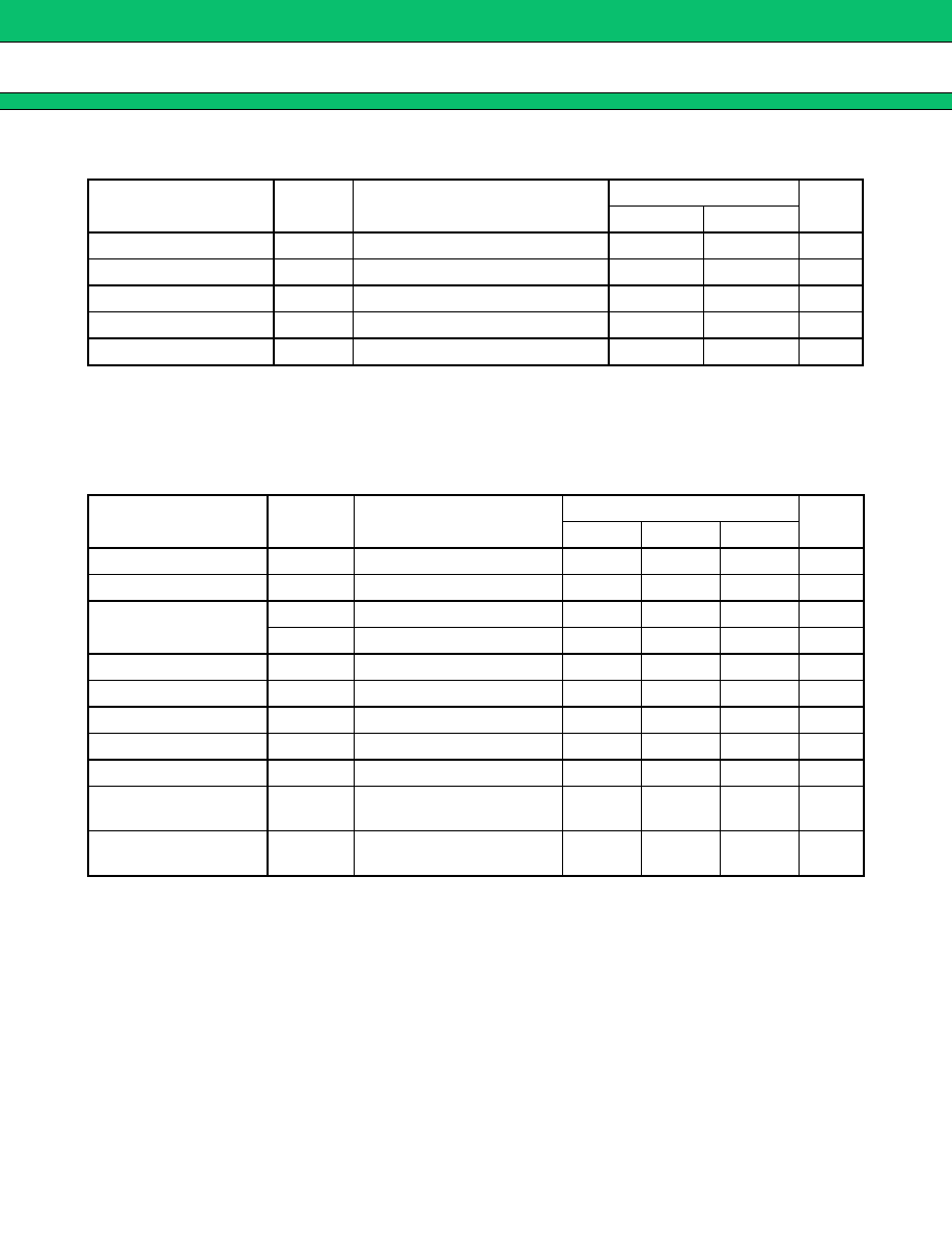
ABSOLUTE MAXIMUM RATINGS
* : The package is mounted on the dual-sided epoxy board (10 cm
◊
10 cm) .
WARNING: Semiconductor devices can be permanently damaged by application of stress (voltage, current,
temperature, etc.) in excess of absolute maximum ratings. Do not exceed these ratings.
s
RECOMMENDED OPERATING CONDITIONS
WARNING: The recommended operating conditions are required in order to ensure the normal operation of the
semiconductor device. All of the device's electrical characteristics are warranted when the device is
operated within these ranges.
Always use semiconductor devices within their recommended operating condition ranges. Operation
outside these ranges may adversely affect reliability and could result in device failure.
No warranty is made with respect to uses, operating conditions, or combinations not represented on
the data sheet. Users considering application outside the listed conditions are advised to contact their
FUJITSU representatives beforehand.
Parameter
Symbol
Conditions
Rating
Unit
Min
Max
Power supply voltage
Vcc
VCC, VCCO terminal
28
V
Output current
Io
OUT1, OUT2, OUT3 terminal
20
mA
Peak output current
I
OP
Duty
5
%
(t
=
1/fosc
◊
Duty)
400
mA
Power dissipation
P
D
Ta
+
25
∞
C
1280*
mW
Storage temperature
T
STG
-
55
+
125
∞
C
Parameter
Symbol
Conditions
Value
Unit
Min
Typ
Max
Power supply voltage
Vcc
VCC, VCCO terminal
7
12
25
V
Input voltage
V
IN
-
INE terminal
0
-
Vcc
-
1.8
V
Output current
I
O
OUT1, OUT2, OUT3 terminal
-
15
15
mA
I
VH
VH terminal
0
30
mA
Oscillation frequency
fosc
250
1200
2600
kHz
Timing capacitor
C
T
22
100
1000
pF
Timing resistor
R
T
4.7
10
22
k
VH terminal capacitor
C
VH
VH terminal
0.1
1.0
µ
F
Soft-start capacitor
C
S
CS1, CS2, CS3 terminal
0.1
1.0
µ
F
Short-circuit detection
capacitor
C
SCP
CSCP terminal
0.01
1.0
µ
F
Operating ambient
temperature
Ta
-
30
+
25
+
85
∞
C