 | –≠–ª–µ–∫—Ç—Ä–æ–Ω–Ω—ã–π –∫–æ–º–ø–æ–Ω–µ–Ω—Ç: MB40578 | –°–∫–∞—á–∞—Ç—å:  PDF PDF  ZIP ZIP |
DS04-28202-6E
FUJITSU SEMICONDUCTOR
DATA SHEET
ASSP
1 CHANNEL 8-BIT VIDEO
A/D CONVERTER
MB40578
s
DESCRIPTION
The Fujitsu MB40578 is a low power ultra-high speed video A/D converter fabricated with Fujitsu Advanced
Bipolar Technology. The MB40578 also adopts the fully-parallel comparison technique (flash method) for high
speed convertion and can convert wide band analog signal such as video signal to digital signal at a sampling
rate of DC through 20 Mega-samples/sec. Because of such high-speed poeration, the MB40578 is suitable for
digital video applications such as the digital TV, video processing with computer, or radar signal processing.
s
FEATURES
∑ Resolution:
8 bits
∑ Linearity error:
±0.2% max. (MB40578)
∑ Maximum conversion rate:
20 MSPS min.
∑ Analog input voltage:
3.0V to 5.0V
∑ Digital I/O level:
TTL compatible
∑ Single power supply:
+5V
∑ Power Dissipation:
480mW typ.
∑ Package:
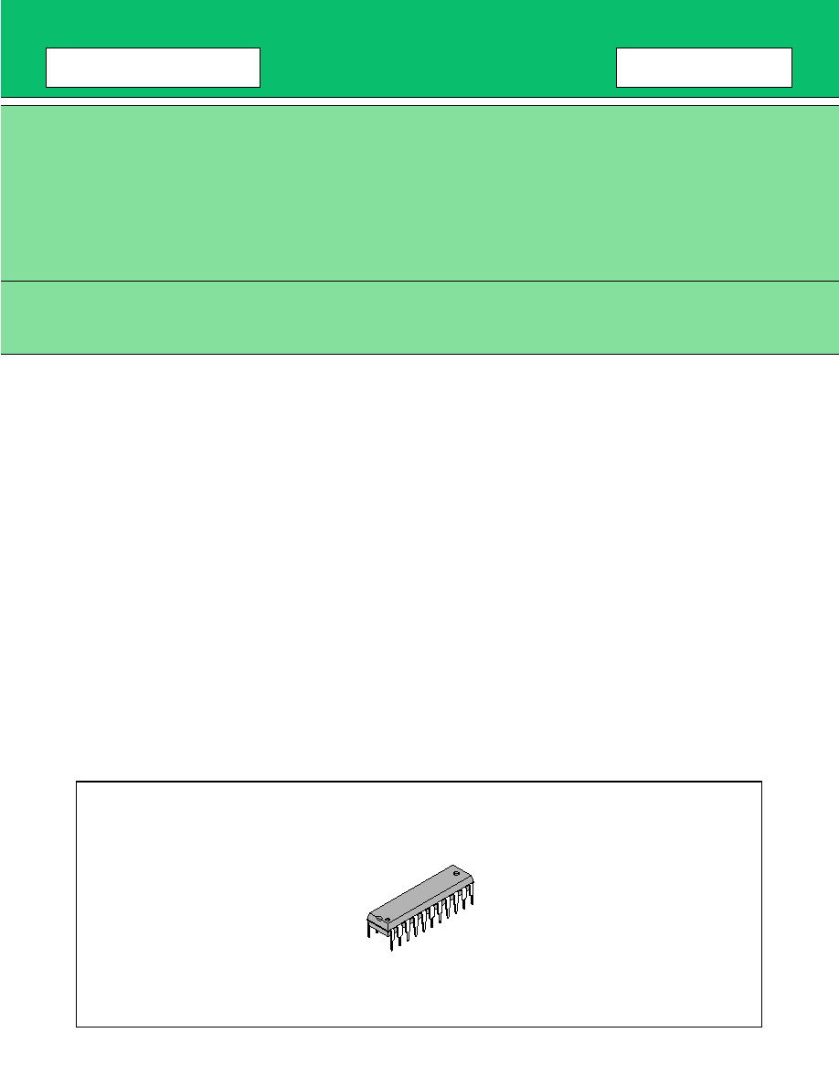
Standard 22-pin DIP Package: Suffix: -P
s
PACKAGE
(DIP-22P-M04)
Plastic DIP, 22 pin
2
MB40578
s
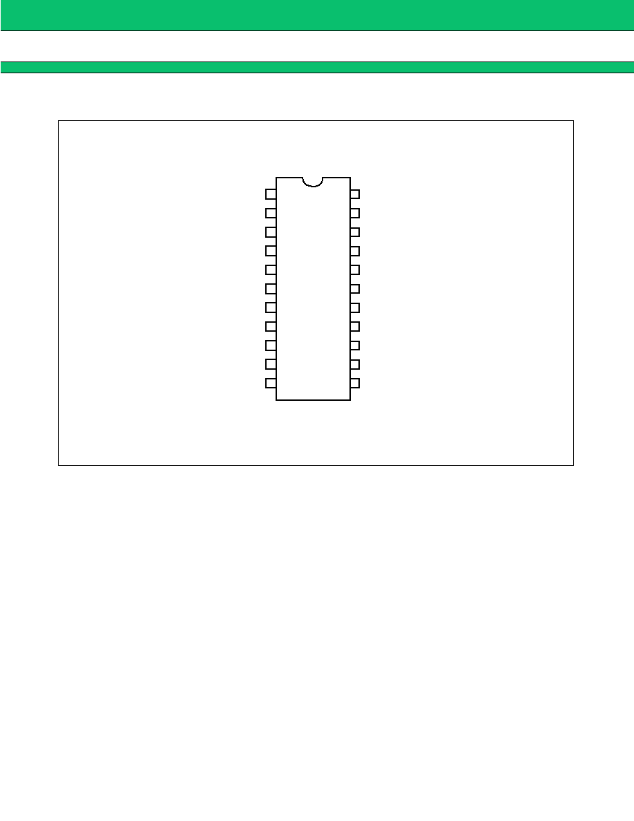
PIN ASSIGNMENT
TOP VIEW
D.GND
(LSB)D
8
D
7
D
6
D
5
D
4
D
3
D
2
(MSB)D
1
CLK
D.GND
A.GND
V
CCD
V
CCA
V
RB
V
INA
V
INA
V
RM
V
RT
V
CCA
V
CCD
A.GND
1
2
3
4
5
6
7
8
9
10
11
22
21
20
19
18
17
16
15
14
13
12
3
MB40578
s
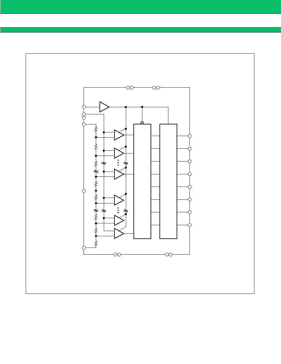
BLOCK DIAGRAM
CLK
V
INA
V
RT
R
1
R
R
R/2
R/2
R
R
R
2
1
2
127
128
254
255
V
RB
V
RM
A.GND
255 to 8
ENCODER
LATCH
&
BUFFER
D
1
(MSB)
D
2
D
3
D
4
D
5
D
6
D
7
D
8
(LSB)
9
2
7
8
6
5
4
3
1 11
D. GND
12 22
V
CCD
V
CCA
21
13
14 20
10
17
15
18
19
16
4
MB40578
s
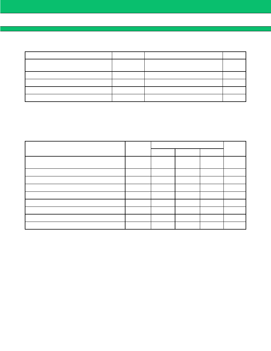
ABSOLUTE MAXIMUM RATINGS
Note: Permanent device damage may occur if the above Absolute Maximum Ratings are exceeded. Functional
operation should be restricted to the conditions as detailed in the operational sections of this data sheet.
Exposure to absolute maximum rating conditions for extended periods may affect device reliability.
s
RECOMMENDED OPERATING CONDITIONS
Notes: *1: Please keep V
CCA
and V
CCD
at the same potential.
*2: V
RB
< V
INA
< V
RT
, V
RT
≠ V
RB
= 2V + 0.1V.
Parameter
Symbol
Rating
Unit
Power supply voltage
V
CCA
V
CCD
≠0.5 to +7.0
V
Digital input voltage
V
IND
≠0.5 to +7.0
V
Analog input voltage
V
INA
≠0.5 to V
CC
+0.5
V
Analog reference voltage
V
RT
, V
RB
≠0.5 to V
CC
+0.5
V
Storage temperature
V
STG
≠55 to +125
∞C
Parameter
Symbol
Value
Unit
Min
Typ
Max
Power supply voltage*
1
V
CCA
V
CCD
4.75
5.00
5.25
V
Analog input voltage*
2
V
INA
3
--
5
V
Analog reference voltage (Top side)*
2
V
RT
--
5
5.1
V
Analog reference voltage (Bottom side)*
2
V
RB
2.9
3
--
V
Digital high-level output current
I
OHD
≠400
--
--
µ
A
Digital low-level output current
I
OLD
--
--
4
mA
Clock pulse width at high level
t
W+
25
--
--
ns
Clock pulse width at low level
t
W≠
25
--
--
ns
Operating temperature
Ta
0
--
70
∞C
5
MB40578
s
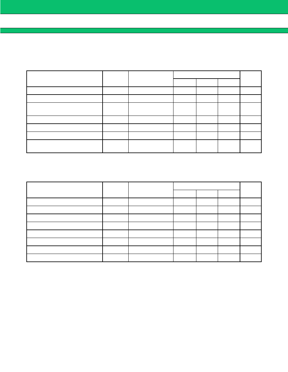
ELECTRICAL CHARACTERISTICS
1. Analog DC Characteristics
(V
CCA
= V
CCD
= 5V ± 5%, Ta = 0 to 70∞C)
2. Digital DC Characteristics
(V
CCA
= V
CCD
= 5V ± 5%, Ta = 0 to 70∞C)
Parameter
Symbol
Condition
Value
Unit
Min
Typ
Max
Resolution
--
--
8
bits
Linearity error
LE
DC
--
--
±0.2
%
Equivalent resistance for analog
input
R
INA
50
--
--
k
Analog input capacitance
C
INA
--
120
230
pF
Analog high-level input current
I
IHA
--
--
150
µ
A
Analog low-level input current
I
ILA
--
--
145
µ
A
Reference current
I
RB
V
RT
= 5V
V
RB
= 3V
≠15
≠9
--
mA
Parameter
Symbol
Condition
Value
Unit
Min
Typ
Max
High-level output voltage
V
OH
I
OH
= ≠400
µ
A
2.7
--
--
V
Low-level output voltage
V
OL
I
OL
= 1.6 mA
--
--
0.4
V
High-level input voltage
V
IHD
2
--
--
V
Low-level input voltage
V
ILD
--
--
0.8
V
Maximum input current
I
ID
V
ID
= 7V
--
--
100
µ
A
High-level input current
I
IHD
V
IHD
= 2.7V
--
0
20
µ
A
Low level input current
I
ILD
V
ILD
= 0.4V
≠400
≠40
--
µ
A
Power supply current
I
CC
--
92
160
mA