
DS04-31102-1E
FUJITSU SEMICONDUCTOR
DATA SHEET
ASSP for Graphics Control
Graphics Display Controller
MB86291A
s
s
s
s
DESCRIPTION
The MB86291A is an evolved version of the Fujitsu MB86290A graphics controller designed for use in a car
navigation system or amusement equipment. The MB86291A is a graphics display controller with a geometry
processor, digital video capture facility, and on-chip SDRAM.
Embedding SDRAM implements data transfer at a higher bandwidth, resulting in faster drawing. Integrating the
geometry processor reduces the CPU load, thereby improving the performance of the entire system.
s
s
s
s
FEATUERS
∑ Operating frequency : 100 MHz (External clock of 14.32 MHz Max)
∑ Geometry processor: Capable of executing operations for geometric transformation and surface front/rear
evaluation.
∑ Memory block: Embedded 16-Mbit SDRAM
∑ Video capture block: Embedded facility to capture digital video images, for example, from TV, capable of easily
implementing "Picture in Picture" and video graphics superimposing.
∑ Host interface: Enables direct connection to various CPUs (Fujitsu SparcLite, Hitachi SH3/4 or NEC V83x) .
(Continued)
s
s
s
s
PACKAGE
208-pin plastic QFP
(FPT-208P-M04)

MB86291A
2
(Continued)
∑ Drawing features:
∑
Drawing at a peak rate of 800 Mpixels per second (at an internal operating frequency of 100 MHz)
∑
2D drawing functions: Point, line, triangle, polygon, BLT, and pattern drawing
∑
3D drawing functions: Point, line, and triangle drawing, and hidden surface removal by Z-buffering
∑
Special effects: Anti-aliasing, bold/dashed-line processing, alpha blending, Gouraud shading, texture
mapping (bilinear filtering, perspective correct) , and tiling
∑ Display features :
∑
Maximum display resolution supported : 1024
◊
768 pixels
∑
Color display either with a color palette of 8 bits per pixel or directly using 5-bit RGB colors of 16 bits per pixel
∑
Overlaying four layers of screen, of which two lower layers can be divided into the left and right parts
∑
Supporting two 64
◊
64-pixel hardware cursors
∑
Output of analog RGB and digital RGB signals
∑
Capable of superimposing using an external synchronization mode
∑ Power-supply voltage : Two power supplies at 2.5 V
±
0.2 V for internal circuits and SDRAM, and 3.3 V
±
0.2 V
for I/O parts
∑ Package: Plastic QFP with 208 pins (with a lead pitch of 0.5 mm)
∑ Process technology : 0.25
µ
m CMOS
MB86291A
3
s
s
s
s
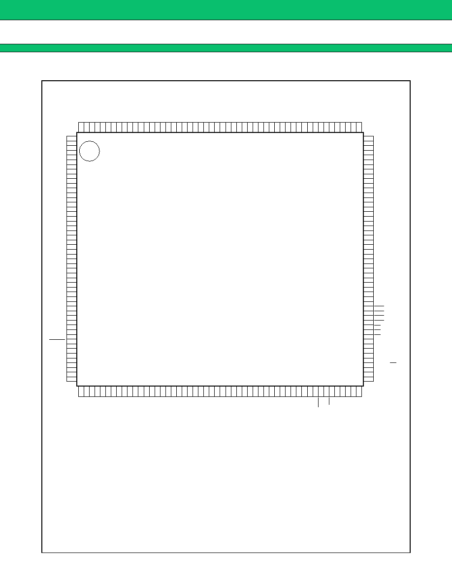
PIN ASSIGNMENT
ACOMPR
156
VRO
154
AVD3
153
AOUTR
152
AVS3
151
AVS2
150
ACOMPG
145
AVS0
144
AOUTB
143
AVD0
142
ACOMPB
141
VDDI
139
A7
138
A6
137
A5
136
A4
135
A3
134
A2
133
VDDI
132
VSS
131
PLLVSS
130
S
129
OSCOUT
128
PLLVDD
127
VDDE
126
VSS
125
CLK
124
OSCCNT
123
VSS
122
VDDI
121
WE3
120
WE2
119
WE1
118
WE0
117
RD
116
BS
115
CS
114
BCLKI
113
VDDI
112
VSS
111
VDDE
110
OPEN
109
DTACK/TC
108
DRACK/DMAAK
107
CKM
106
TESTH4
105
VSS
140
AVD2
149
AVS1
148
AOUTG
147
AVD1
146
VREF
155
1
3
4
5
6
7
12
13
14
15
16
18
19
20
21
22
23
24
25
26
27
28
29
30
31
32
33
34
35
36
37
38
39
40
41
42
43
44
45
46
47
48
49
50
51
52
17
8
9
10
11
2
VSS
R0
R1
VCC1
VSS
R2
R7
VCC2
VDDE
VSS
VCC3
G0
G1
G2
G3
VSS
G4
G5
G6
G7
VDDE
B0
B1
B2
B3
VSS
B4
B5
B6
B7
VCC4
VDDI
VSS
VCC5
VDDE
CLKSEL0
CLKSEL1
RESET
MODE0
MODE1
VSS
VCC6
MODE2
TESTL0
VCC7
VSS
VDDI
R3
R4
R5
R6
VCC0
VSS
208
HSYNC
206
VSYNC
205
CSYNC
204
VSS
203
DCLKO
202
VDDE
201
VI7
200
VI6
199
VI5
198
VI4
197
VI3
196
VI2
195
VI1
194
VI0
193
VDDI
192
VSS
191
DCLKI
190
EO
189
RESERVE
188
RESERVE
187
GV
207
RESERVE
186
RESERVE
184
TESTH5
183
CCLK
182
VDDE
181
VSS
180
A24
179
A23
178
A22
A21
177
A20
176
A19
175
A18
174
A17
173
A16
172
VDDI
171
VSS
170
A15
169
A14
168
A13
167
A12
166
RESERVE
185
A11
165
A9
163
A8
162
TESTL1
161
VDDE
160
VDDI
159
158
157
VSS
A10
164
TESTH0
VDDI
D0
D1
D2
D3
D4
D5
D6
D7
VDDE
VSS
D8
D9
D10
D11
D12
D13
D14
VDDI
VSS
VSS
D15
D17
D18
VDDE
D19
D20
D21
D22
D23
D24
VSS
VDDI
D25
D26
D27
D28
D29
VSS
VDDE
D30
D31
D16
RDY
INT
VSS
VDDI
TESTH1
TESTH2
TESTH3
DREQ
53
55
56
57
58
59
60
61
62
63
64
65
66
67
68
69
70
71
72
73
74
54
75
77
78
79
80
81
82
83
84
85
86
87
88
89
90
91
92
93
94
95
76
96
98
99
100
101
102
103
104
97
(TOP VIEW)
VSS/AVS/PLLVSS
VDDH/VDDE
VDDL/AVD/PLLVDD/VCC/VDDI
AVD
PLLVDD
VCC
OPEN
TESTL0/TESTL1
TESTH0 ~ TESTH5
RESERVE
Notes :
∑
The AVD and PLLVDD should be separated on the board.
∑
Insert a bypass capacitor with a superior high-frequency characteristic between the power
supply and ground. Place the capacitor as near the pins as possible.
: Ground
: 3.3 V power supply
: 2.5 V power supply
: Analog power supply
: PLL power supply
: Internal DRAM power supply
: Do not connect anything.
: Input the low level.
: Input the high level.
: Input the high level.
MB86291A
4
s
s
s
s
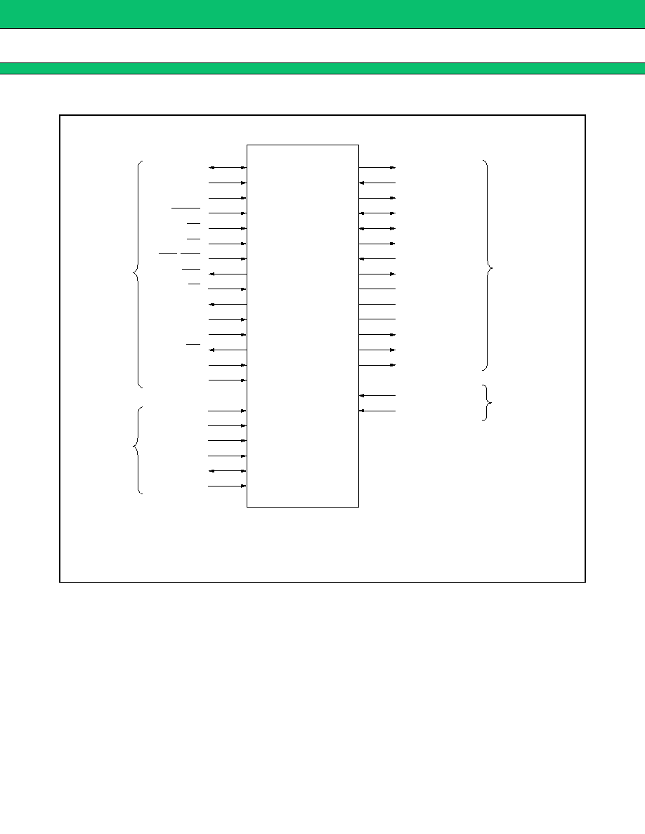
PIN DESCRIPTION
D0-D31
A2-A24
BCLKI
RESET
CS
RD
WE0-WE3
RDY
BS
DREQ
DRACK
DTACK
INT
TESTL, TESTH
CLK
S
CKM
OSCOUT
OSCCNT
DCLKO
DCLKI
HSYNC
VSYNC
CSYNC
EO
GV
VREF
VRO
R0-R7
G0-G7
B0-B7
CCLK
VI0-VI7
MB86291A
Graphics Controller
HQFP208
ACOMPR, ACOMPG,
ACOMPB
AOUTR, AOUTG,
AOUTB
CLKSEL0-
CLKSEL1
MODE0-
MODE2
Vide output
interface
Host CPU
interface
Clock
Vide capture
interface

MB86291A
5
∑
∑
∑
∑
Host Interface Pins
Note : The host interface can connect the MB86291A to the SH4 (SH7750) or SH3 (SH7709) from Hitachi Ltd.
the V832 from NEC, or to the SPARClite (MB86833) from Fujitsu without any external circuit in between.
(Using the SRAM interface allows the MB86291A to use another CPU.) The host CPU is set by the
MODE0 and MODE1 pins as shown below.
Note : The MODE2 pin can be used to set the Ready signal level to be used upon completion of the bus cycle. To
use the MODE2 signal at "H" level, set the software setting to two cycles.
Pin Name
Input/output
Function
MODE0 to MODE2
Input
Host CPU mode/Ready mode select
RESET
Input
Hardware reset
D0 to D31
Input/output
Host CPU bus data
A2 to A24
Input
Host CPU bus address (Connect A[24] to MWR in V832 mode.)
BCLKI
Input
Host CPU bus clock
BS
Input
Bus cycle start signal
CS
Input
Chip select signal
RD
Input
Read strobe signal
WE0
Input
D0 to D7 write strobe signal
WE1
Input
D8 to D15 write strobe signal
WE2
Input
D16 to D23 write strobe signal
WE3
Input
D24 to D31 write strobe signal
RDY
Output
Tristate
Wait request signal
("0" for wait state with SH3; "1" for wait state with SH4, V832, or SPARClite)
DREQ
Output
DMA request signal (active low with both SH and V832)
DRACK/DMAAK
Input
DMA request acknowledge signal (Connect this to DMAAK in V832 mode.
Active high with both SH and V832.)
DTACK/TC
Input
DMA transfer strobe signal (Connect this to TC in V832 mode. SH = active
high, V832 = active low)
INT
Output
Host CPU interrupt signal (SH = active low, V832 = active high)
TEST0, TEST1,
TESTH0 to TESTH5
Input
Test signal
MODE1 pin
MODE0 pin
CPU Type
L
L
SH3
L
H
SH4
H
L
V832
H
H
SPARClite
MODE2 pin
Ready signal mode
L
Set RDY signal to "Not Ready" level upon completion of bus cycle.
H
Set RDY signal to "Ready" level upon completion of bus cycle.