DS04-26903-3E
FUJITSU SEMICONDUCTOR
DATA SHEET
ASSP
CMOS
Dolby Digital (AC-3) Decoder LSI
MB86342B
s
DESCRIPTION
Dolby Digital (AC-3) is a perceptual digital audio coding technique of unprecedented efficiency, quality and
versatility.
Fujitsu has developed Dolby Digital (AC-3) 5.1-ch full decodable LSI.
This LSI is certificated as " Dolby Digital (AC-3) Decoder LSI " by Dolby Laboratories Licensing Corporation.
s
FEATURES
∑ Dolby Digital (AC-3) 5.1ch Full Decode
≠ All bit-rate and All sampling frequency
≠ Down Mix
≠ Dialog Normalization
≠ Dynamic-range Compression
≠ Noise sequencer (Test tone)
≠ Each channel can be independently set
≠ Output Bass Management (config-1, 2, 3)
∑ Dolby Pro Logic Decode
∑ Dolby Digital (AC-3) + Dolby Pro Logic Decode
∑ 16/18/20bit Audio Data Input/Output
(Continued)
s
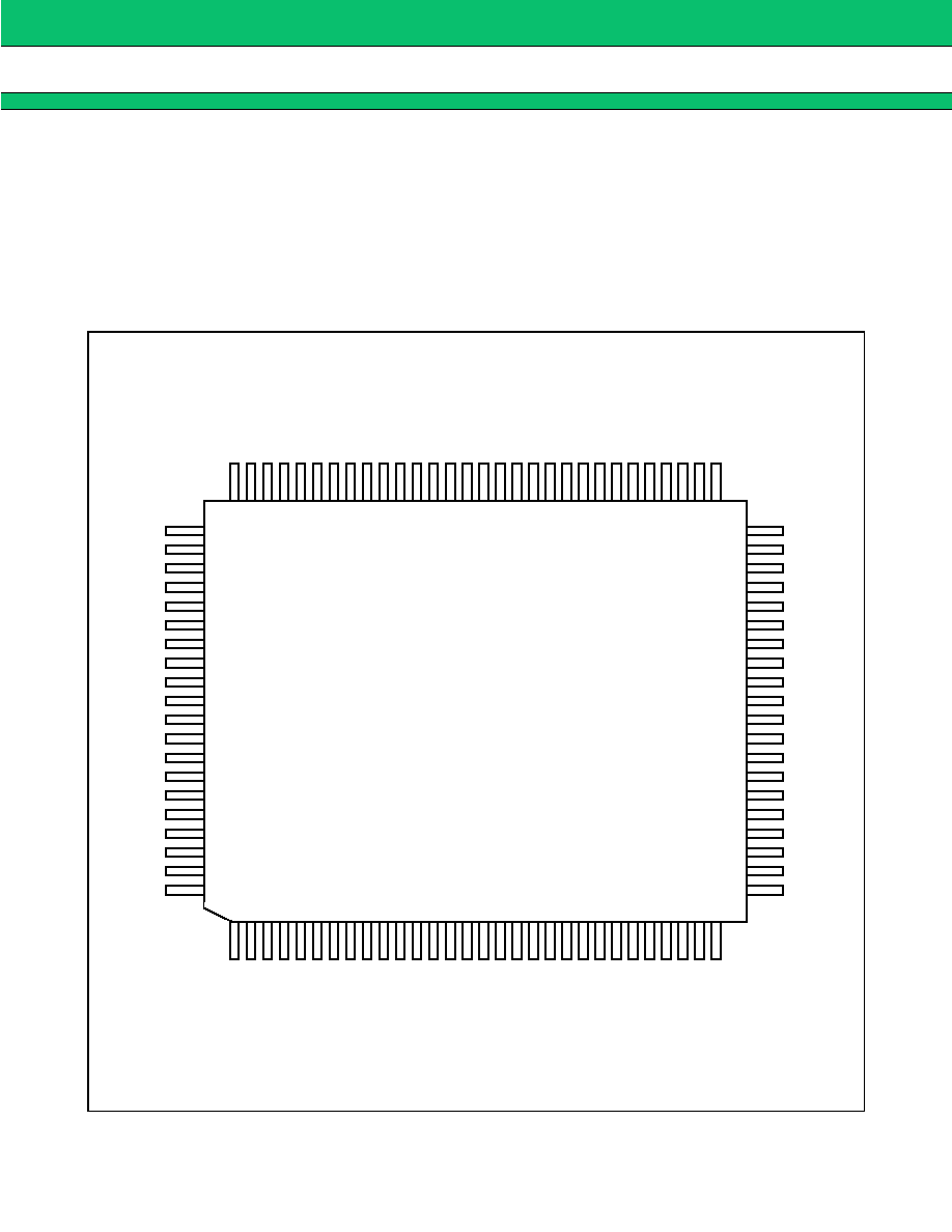
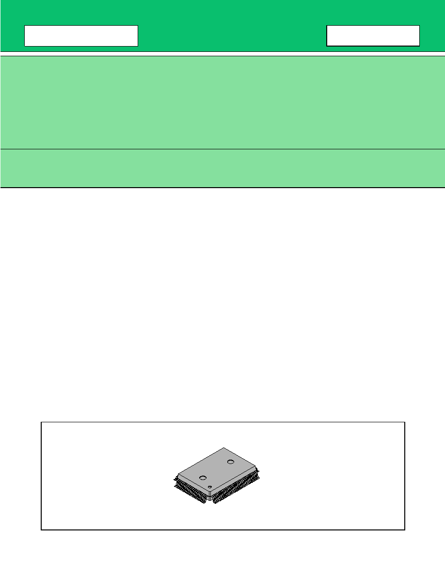
PACKAGE
Note: Dolby, AC-3, Pro Logic and double-D are trademarks of Dolby Laboratories Licensing Corporation.
(FPT-100P-M06)
100-pin Plastic QFP

3
MB86342B
s
PIN DESCRIPTION
Pin No.
Pin name
I/O
Function
5
MCLK1
I
Clock input
6
MCLK2
I/O
Clock input/output
1
XRST
I
Reset signal input
8
SCKO
O
System clock output
12
MS
I
Master/Slave select input
L: Master (X'tal) H:Slave (external clock)
16
SYNC
I
Synchronous/Asynchronous select input
2
EXTIN
I
System clock input (384fs)
13, 14
FS1, FS2
I
Sampling frequency switching signal input
7
KFSIO
I/O
Audio input/output clock (384fs)
9
PM
I
Test pin (usually clipped to GND)
10
PSTOP
I
PLL and crystal oscillator control signal
11
EXLOCK
I
Lock signal input of EXTIN
41
HCLK
I
Clock input for serial input-data of host interface
43
HDIN
I
Serial data input of host interface
44
HDOUT
O
Serial data output of host interface
42
HCS
I
Chip-select signal input of host interface
45
BST
I
Usually clipped to GND
30 to 32, 35 to 39
GP0 to GP7
I/O
Input/output of 8-bit general port data
17
LRCKI1
I/O
Sampling clock input/output for audio interface serial data
18
BCKI1
I/O
Bit clock input/output for audio interface serial data
20
LRCKI2
I
Sampling clock input for audio interface serial data
21
BCKI2
I
Bit clock input for audio interface serial data
19, 22
SD1, SD2
I
Serial data input of audio interface
23
LRCKO
O
Sampling clock output for audio interface serial data
24
BCKO
O
Bit clock output for audio interface serial data
25 to 27
SDO1 to SDO3
O
Serial data output of audio interface
46
MOD
I
Bus-mode control signal input
47
CS
O
Chip-select signal output for external SRAM interface
48
WE
O
Write enable signal output for external SRAM interface
49 to 52, 55 to 64, 66, 67 A00 to A15
O
Address data output of external SRAM interface
68 to 77,80 to 82
85 to 89, 91, 92
D00 to D19
I/O
Data input/output of external SRAM interface
93
ICCLK
O
Clock output for emulator
94
ICBRK
I
External break control signal input for emulator
95, 96
ICD0, ICD1
I/O
Input/output signal for data/address of emulator
97 to 99
ICS0 to ICS2
O
Status signal output for emulator

5
MB86342B
s
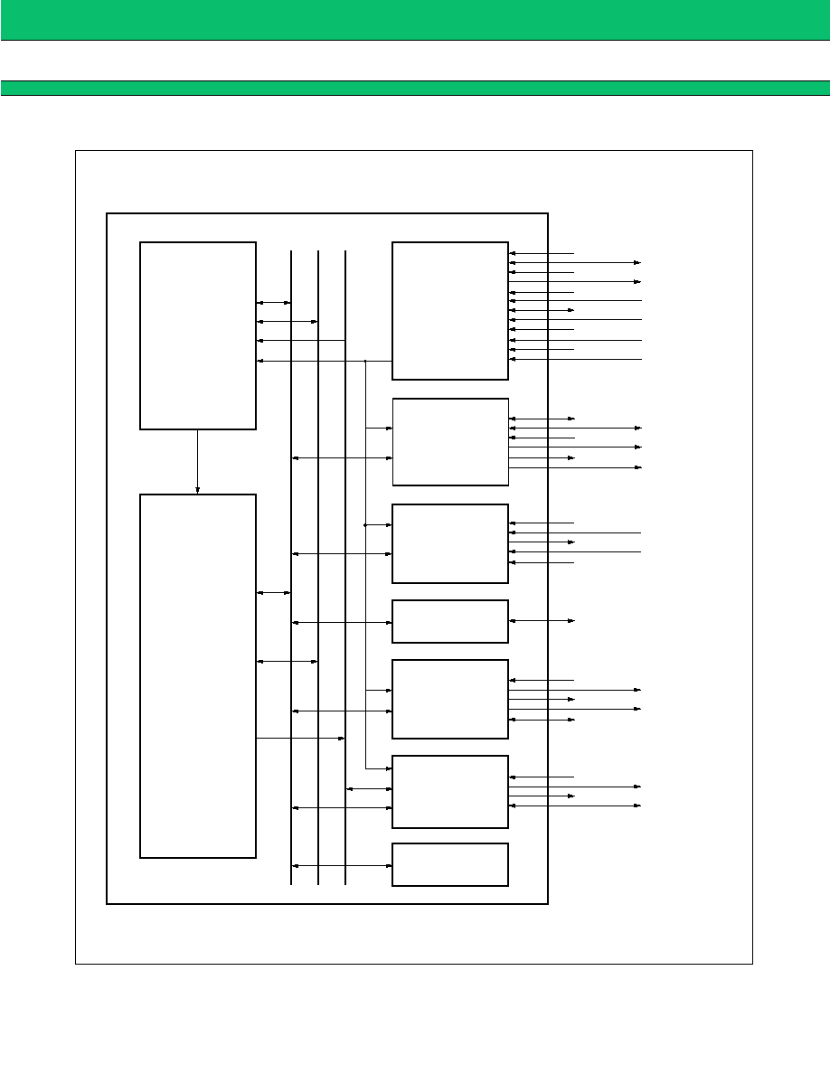
FUNCTION OF EACH BLOCK
MCORE : MUCAP Core
MUCAP Core is a 20-bit fixed point DSP core. This core operates MOVE, BRANCH,
INTERRUPT, ADDRESSING and ARITHMETIC operations.
CLKGM : Clock Generation Module
This module generates internal and external clock. two type of clocks are generated external
clocks and clock from external crystal oscillator.
ADIF
: Audio Interface Module
This module is an interface of input/output serial audio data to external.
∑ 2-channels of input port, and 3-channel of output port.
∑ 2-audio data input registers and 6-output registers ( 20-bit ).
HSTIF
: Host Interface Module
This module transfers asynchronous serial data to host CPU, which has input data register and
output data register(20-bit).
GP
: General Port Module
This module has a 8-bit direction register and 8-bit data register. Each port is independent as
a 1pin input/output general port(total 8pins).
EXMIF
: External Memory Interface Module
This module reads and writes data to external memory(SRAM), which has 3-byte data read/
write mode and 1word(20bit) data read/write mode.
This module uses in-service-register in order to read and write 3-byte data.
EMUIF
: Emulator Interface Module
This module is used for in circuit emulation.
LOG
: LOG Module
This module has registers to refer to table data for the operation of logarithmic functions.
MEM
: Memory Module
This module restores data and programs.