 | –≠–ª–µ–∫—Ç—Ä–æ–Ω–Ω—ã–π –∫–æ–º–ø–æ–Ω–µ–Ω—Ç: MB86434PF | –°–∫–∞—á–∞—Ç—å:  PDF PDF  ZIP ZIP |
DS04-23003-1E
FUJITSU SEMICONDUCTOR
DATA SHEET
ASSP
CMOS
5V Single Power Supply Audio
Interface Unit (AIU)
MB86434
s
DESCRIPTION
The FUJITSU MB86434 is an AIU (audio interface unit) LSI for +5 V single-power source digital telephone devices,
manufactured using CMOS process technology. The codec transmission filter characteristics meet G.712 standards,
and can handle input and output in A-Law,
µ
-Law and linear conversion modes. The MB86434 also contains the
necessary DTMF, microphone and receiver amps for telephone devices.
s
FEATURES
∑ +5 V single power supply
∑ Low power consumption: muting settings for each operating mode
Normal operation : 8.2 mA typ (speaker amp mute)
Tone generation
: 1.8 mA typ (speaker amp mute)
Standby mode
: 0.5 mA typ
∑ On-chip codec filter meets G.712 standards
∑ Selection of codec conversion methods (A-law,
µ
-law, linear)
∑ On-chip low-noise microphone amp (2-channel) (unity gain frequency: 1MHz)
∑ On-chip receiver speaker amps (32
BTL type: 10 mW
MIN
)
∑ On-chip tone speaker amp (32
BTL type: 200 mW
MIN
)
∑ On-chip earphone speaker amps (32
single type: 5 mW
MIN
)
(Continued)
s
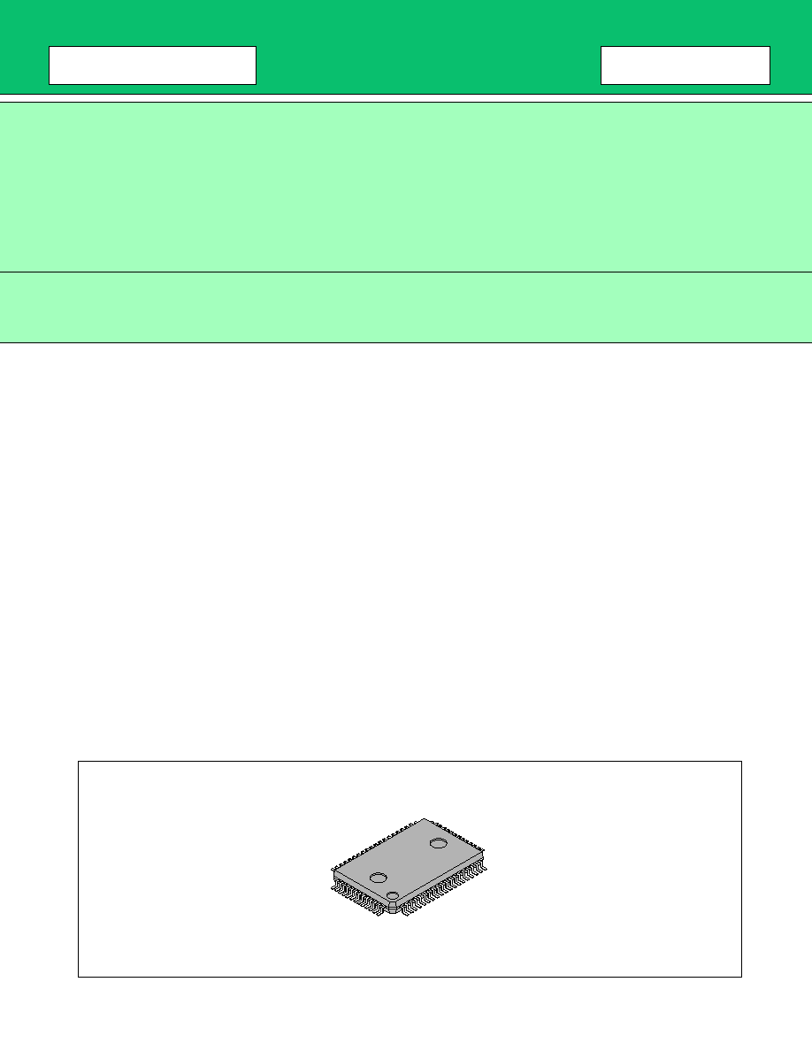
PACKAGE
64 pin, Plastic QFP
(FPT-64P-M07)
MB86434
2
(Continued)
∑ On-chip electronic volume gain adjustments (sending, receiving, tone)
∑ On-chip accessory output circuits
∑ DTMF generator function
∑ Service tone generation
∑ CMOS compatible input/output
s
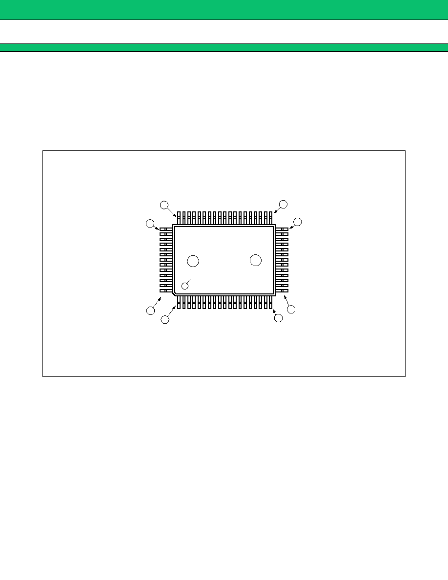
PIN ASSIGNMENT
(FPT-64P-M07)
(TOP VIEW)
19
20
32
33
51
52
64
1
INDEX
MB86434
3
s
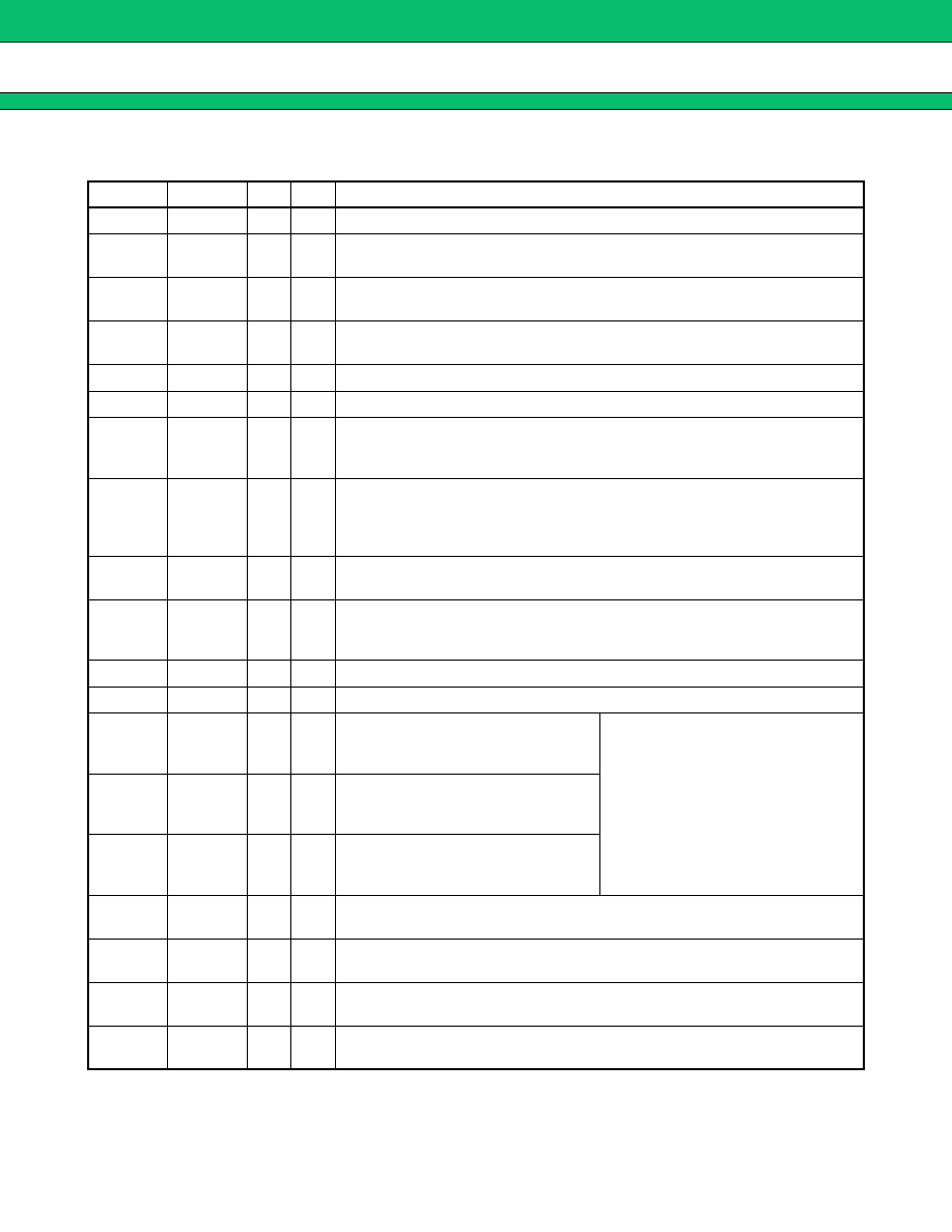
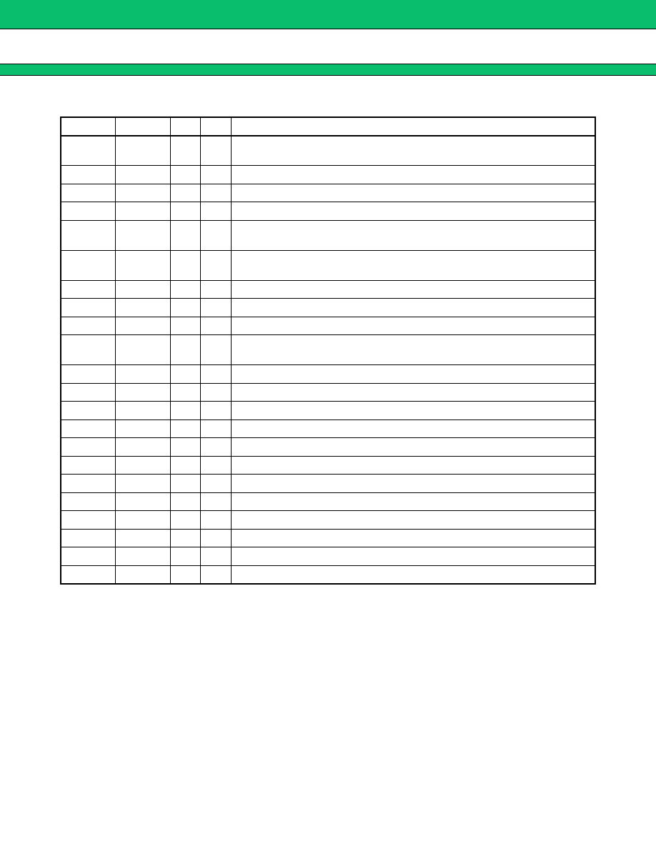
PIN DESCRIPTION
(Continued)
Pin No.
Symbol
I/O
A/D
Description
1
CAG
G
A
Analog ground pin for codec block. To be set to 0 V.
2
VRH
O
A
Bypass capacitor connector pin for the A/D D/A reference voltage generator
circuit. Place capacitor between VRH and CAG pins.
3
SGC
O
A
Bypass capacitor connector pin for the signal ground potential generator
circuit. Place capacitor between SGC and CAG pins.
4
VDDAC
P
A
Analog power supply pin for codec block. To be set within range 4.75 to
5.25 V.
5
N.C.
--
--
Not connected. To be left open.
6
N.C.
--
--
Not connected. To be left open.
7
SYNC
I
D
PCM codec send/receive synchronization signal input pin. Operating clock
frequencies 8 kHz. CMOS interface. Other frequencies may cause codec
block to power-down.
8
CLK
I
D
Send/receive PCM signal series bit rate setting input pin. Data rate for
µ
-law,
A-law modes may be set to any level in the range 64 k to 3.152 MHz, and for
linear in the range 256 k to 3.152 MHz. Constant H or L level signal will
cause part of codec block to power-down. CMOS interface.
9
DIN
I
D
PCM signal input pin. This signal is picked up internally at the fall of the CLK
signal. CMOS interface.
10
DOUT
O
D
PCM signal output pin. Data is output in sync with the rise of the CLK signal.
After data output, loses PLL synchronization, and at power-down this signal
is fixed at H level. CMOS interface.
11
VDD
P
D
Digital power supply pin. To be set within range 4.75 to 5.25 V.
12
DG
G
D
Digital ground pin. To be set to 0V.
13
PSC0
I
D
Power-down control signal input pin.
CMOS interface. Used with PSC1,2
pins for power-down settings.
PSC 2 1 0
0 0 0 Full power-down
1 0 0 V
REF
operating
-- 1 0 Tone operating
-- -- 1 All operations available
(--: value not determined)
14
PSC1
I
D
Power-down control signal input pin.
CMOS interface. Used with PSC0,2
pins for power-down settings.
15
PSC2
I
D
Power-down control signal input pin.
CMOS interface. Used with PSC0,1
pins for power-down settings.
16
SRD
I
D
9-bit serial data input pin. CMOS interface. Data is written at the rise of the
signal from this pin.
17
SRC
I
D
Clock input pin for 9-bit serial data writing. CMOS interface. Data is written
at the rise of this pin.
18
STB
I
D
Serial data latch strobe signal. Data is latched by the L level signal. CMOS
interface. On-chip pull-down resistance.
19
XPRST
I
D
Digital reset signal input pin. CMOS interface. L level: internal latch
initialization H level: normal operation
MB86434
4
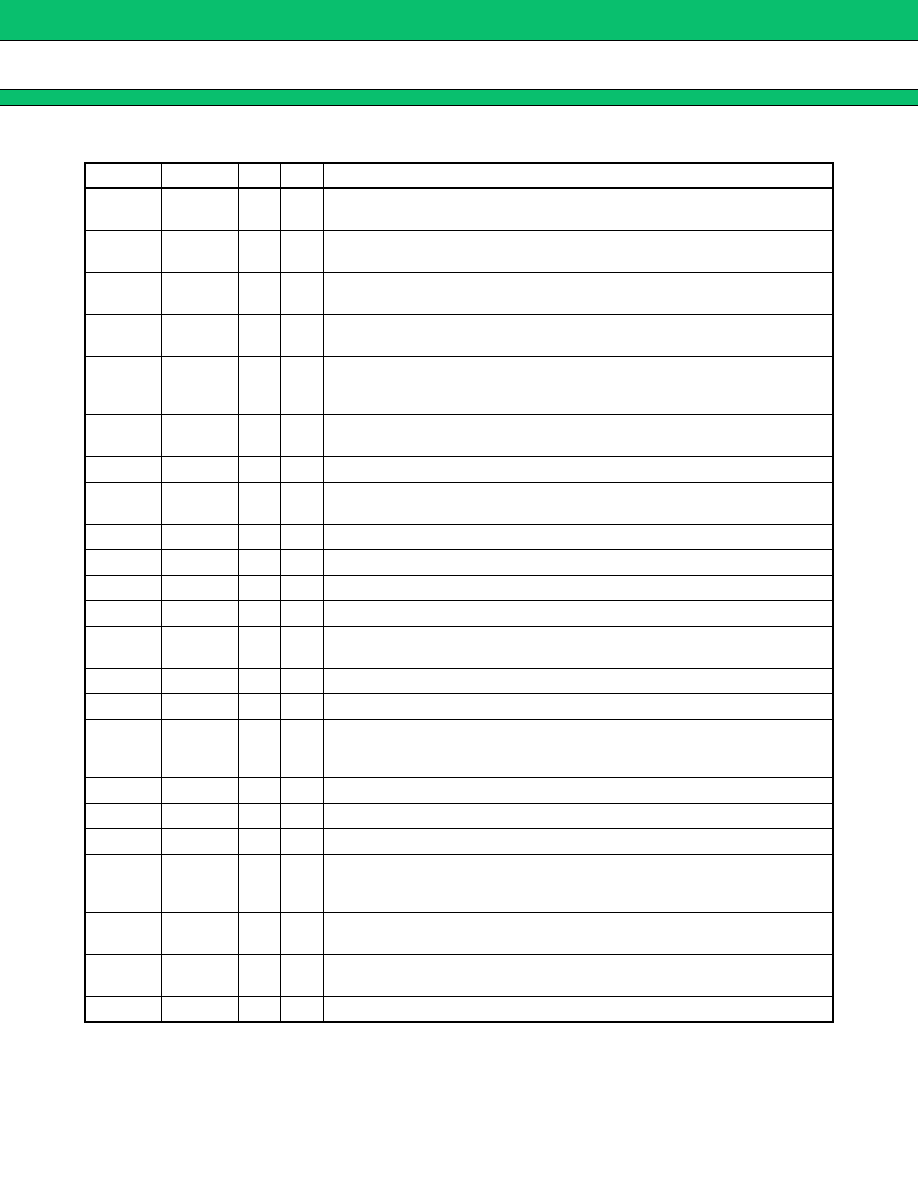
(Continued)
Pin No.
Symbol
I/O
A/D
Description
20
LO0
O
D
External control latch output pin. Outputs value D
0
of address 1000. CMOS
interface.
21
LO1
O
D
External control latch output pin. Outputs value D
1
of address 1000. CMOS
interface.
22
LO2
O
D
External control latch output pin. Outputs value D
2
of address 1000. CMOS
interface.
23
LO3
O
D
External control latch output pin. Outputs value D
3
of address 1000. CMOS
interface.
24
TCLK
I
D
Tone generator clock input pin. Can be used as a tone CLK signal by using
address 1110 D4D3 to subdivide the internal clock signal by factors of 1/1,
1/2, 1/4. CMOS interface.
25
TONC
I
D
Tone generator cycle control input pin. CMOS interface. Hlevel signal
outputs tone.
26
LED
O
D
Ring LED control output pin. CMOS interface.
27
TENV
I
A
Can be used to generate tone envelope, by placing capacitor between
grounds and turning SW11 on/off.
28
SWO
I/O
A
Analog switch 10 input/output pin. Controls address 0111 D
0
.
29
SWI
I/O
A
Analog switch 10 input/output pin.
30
DSDT
I
A
Accessory input. Can be connected to RAUD by switching paths.
31
TONEO
O
A
Tone signal output pin.
32
RAUD
O
A
Output pin for external speaker, or audio test signal. Can be connected to
DSDT by switching paths.
33
VDDSP1
P
A
Speaker amp power supply pin. To be set within range 4.75 to 5.25 V.
34
JEAR
O
A
Earphone speaker amp output pin. Capable of 5 mW output at 32
load.
35
XEAR
O
A
Receiver speaker amp output pin. Internally connected to EAR and BTL.
Maximum output of 10 mW can be obtained at 32 W load by connecting
speaker between EAR and XEAR.
36
EAR
O
A
Receiver speaker amp output pin. Connected to XEAR and BTL.
37
SPG1
G
A
Speaker amp ground pin. To be set to 0 V.
38
SPG2
G
A
Speaker amp ground pin. To be set to 0 V.
39
XTONE
O
A
Speaker amp tone output pin. Internally connected to TONE and BLT.
Maximum output of 10 mW can be obtained at 32
load by connecting
speaker between TONE and XTONE.
40
TONE
O
A
Speaker amp tone output pin. When speaker amp is not used for tone,
TONE should be shorted to IMTON.
41
IMTON
I
A
Speaker drive inverted (≠) signal input pin. Can be used to adjust gain by
connecting resistance to TONE and IMTON.
42
VDDSP2
P
A
Speaker amp power supply pin. To be set within range 4.75 to 5.25 V.
MB86434
5
(Continued)
Pin No.
Symbol
I/O
A/D
Description
43
BBI
O
A
AMP3 output pin. Should be included in HPF together with IM3, to prevent
DC offset from entering speakers.
44
IM3
I
A
AMP3 inverted (≠) signal input pin.
45
BTO
O
A
Receiving volume adjustment circuit output pin.
46
OP2
O
A
AMP2 output pin. If AMP2 is not used, IM2 should be shorted to OP2.
47
IM2
I
A
AMP2 inverted (≠) signal input pin. Can form a circuit with OP2 to add
sidetone or tone. Melody circuits, if used, can also be connected here.
48
OP1
O
A
AMP1 output pin. Can form a circuit with IM1 to include LPF or HPF in
receiving block. If AMP1 is not used, IM1 should be shorted to OP1.
49
IM1
I
A
AMP1 inverted (≠) signal input pin.
50
PTBO
O
A
PCM receiver output pin.
51
BAG
G
A
Analog ground pin for sending, receiving blocks. To be set to 0 V.
52
VDDAB
P
A
Analog power supply pin for sending, receiving blocks. To be set within
range 4.75 to 5.25 V.
53
XJMIC
I
A
Microphone amp (2) non-inverted (+) signal input pin.
54
JMIC
I
A
Microphone amp (2) inverted (≠) signal input pin.
55
JMICO
I
A
Microphone amp (2) output pin.
56
XMIC
I
A
Microphone amp (1) non-inverted (+) signal input pin.
57
MIC
I
A
Microphone amp (1) inverted (≠) signal input pin.
58
MICO
O
A
Microphone amp (1) output pin.
59
SGO
O
A
Sending block signal ground potential output pin. Buffers SGC voltage.
60
BBO
O
A
Sending analog signal output pin.
61
N.C.
--
--
Not connected. To be left open.
62
N.C.
--
--
Not connected. To be left open.
63
BTPI
I
A
PCM ENCODE block input OP amp negative input pin.
64
BTPO
O
A
PCM ENCODE block input OP amp output pin.