DS04-22415-1E
FUJITSU SEMICONDUCTOR
DATA SHEET
ASSP Communication Control
CMOS
SCSI-II Protocol Controller
(with single-ended driver/receiver)
MB86604L
s
DESCRIPTION
The Fujitsu MB86604L is a single-ended transmission type SCSI-II Protocol Controller (SPC) with a single-ended
driver/receiver. The MB86604L facilitates interface control between small/medium host computer and peripheral
devices (such as a hard disk and printer). The specifications conform to the SCSI-II Standard.
The MB86604L supports high-speed synchronous transfer, the MPU/DMA independent system data bus, and
user programmable command set to enable configuration of high-performance systems.
It can also have the phase-to-phase sequence control function to reduce the program overhead of the host MPU.
The MB86604L incorporate with a single-ended type SCSI driver/receiver which can drive 48 mA of large-current,
and so, the device can be directly connected with the SCSI bus.
The device can operate with +5 V single-power supply and in up to 40 MHz clock frequency. As for package, a
100-pin plastic small quad flat package is available.
s
FEATURES
SCSI Bus Interface:
� Conforming to the SCSI-II standard
� Operatable as Initiator and target
(Continued)
s
PACKAGE
100 pin, Plastic LQFP
(FPT-100P-M05)

2
MB86604L
(Continued)
� Two types of high-speed data transfer:
� Synchronous data transfer (Max. 10 Mbytes/s, max. 32 offsets, 32-step transfer rate)
� Asynchronous data transfer (Max. 5 Mbyte/s)
� Transfer parameters (transfer mode, transfer rate, transfer offset) can be set for up to 7 connected devices.
� Single-ended transmission type (Maximum cable length: 6 m):
� On-chip single-ended driver/receiver which can drive 48 mA of "L" level output current
� Directly connectable with the SCSI bus
� On-chip three-state bidirectional I/O buffers for SCSI REQ and ACK pins (DB7-DB0, DBP, ATN, MSG, C/D, I/
O pins can be selected from either three-state or open-drain buffer by controlling the TEST pins input.)
Transfer Operation:
� Automatic response to selection/reselection (Preset receiving operation can perform at the selection/
reselection.):
� Initiator: Automatically operates until message received without command issue.
� Target: Automatically operates until command received without command issue.
� Automatic receiving:
� Initiator: Automatically receives information for new phase to which target transited without command issue.
� Target: Automatically receives message from initiator when initiator generates attention condition.
� On-chip 32-byte data register (FIFO) for data phase
� On-chip two (send-only and receive-only) 32-byte data buffers for message, command, and status phases
� On-chip 16-bit transfer block register and 24-bit transfer byte register enabling 1 Tbytes transfer (1 Tbytes: 16
Mbytes
�
64 k blocks)
� On-chip independent data transfer bus enabling the MPU operation during the data transfer
� Parity through/generate can be specified.
System Bus Interface:
� 8-bit or 16-bit separate MPU and DMA buses
� Directly connectable with a 80 series or 68 series MPU
� Two types of transfer operation:
� Program transfer
� DMA transfer (Burst/Handshake)
Command Set:
� Supports sequential commands and programmable commands in addition to ordinary commands
� Command queuing (Command can be continuously issued by putting tags to commands in command phase.)
� On-chip 256-byte memory for command programming memory and command queuing buffer
Others
� Process: CMOS process
� Supply Voltage: Single +5 V
� Input System Clock: 20 MHz/30 MHz/40 MHz
� Package: 100-pin plastic LQFP
3
MB86604L
s
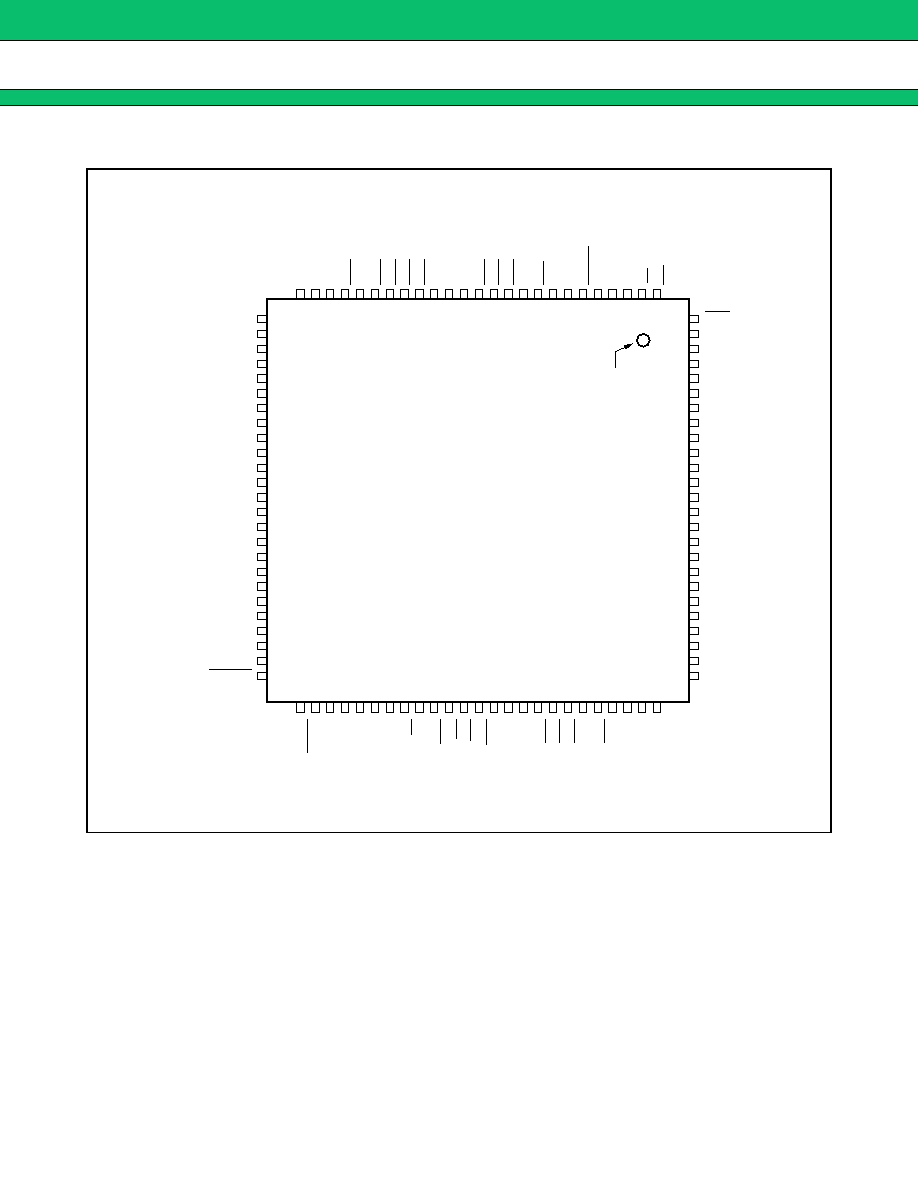
PIN ASSIGNMENT
INDEX
100
99
98
97
96
95
94
93
92
91
90
89
88
87
86
85
84
83
82
81
80
79
78
77
76
1
2
3
4
5
6
7
8
9
10
11
12
13
14
15
16
17
18
19
20
21
22
23
24
25
75
74
73
72
71
70
69
68
67
66
65
64
63
62
61
60
59
58
57
56
55
54
53
52
51
BHE
UDP
D 15
D 14
D 13
D 12
D 11
D 10
D 9
D 8
V
SS
D 7
D 6
D 5
D 4
D 3
D 2
D 1
D 0
LDP
CS 1
V
SS
V
DD
CS 0
A4
26
27
28
29
30
31
32
33
34
35
36
37
38
39
40
41
42
43
44
45
46
47
48
49
50
WR
RD
V
DD
V
SS
CLK
RESET
INT
MODE
DBP
V
SS
DB 7
DB 6
DB 5
V
DD
V
SS
V
SS
DB 4
DB 3
DB 2
DB 1
V
SS
DB 0
TEST 1
TMOUT
A3
A2
A1
A0
ATN
V
SS
BSY
ACK
RST
V
SS
V
SS
V
DD
MSG
SEL
C/D
REQ
V
SS
I/O
TEST2
TP
V
SS
V
DD
DREQ
DACK
(FPT-100P-M05)
I OWR
I ORD
V
DD
V
SS
DMA 0
LDMDP
DMD 0
DMD 1
DMD 2
DMD 3
DMD 4
DMD 5
DMD 6
DMD 7
V
SS
DMD 8
DMD 9
DMD 10
DMD 11
DMD 12
DMD 13
DMD 14
DMD 15
UDMDP
DMBHE
(OPEN)
(OPEN)
(TOP VIEW)
4
MB86604L
s
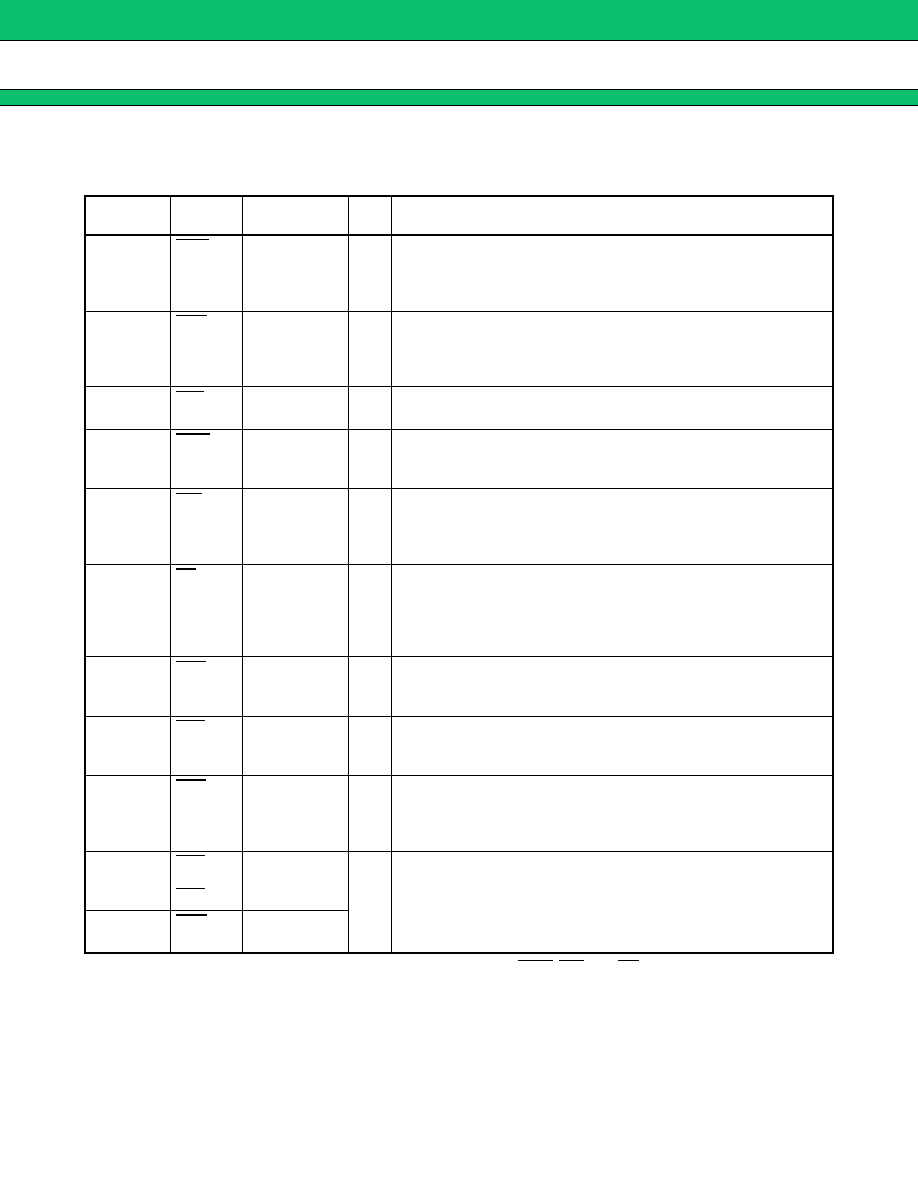
PIN DESCRIPTION
1.
SCSI Interface
* : Regarding the status of information transfer which is indicated by MSG, C/D, and I/O pins, See Table Phase Status.
Pin
number
Symbol
Pin name
I/O
Function
60
REQ
Request
I/O
Transfer request signal in the information transfer phases from
target to initiator. The input signal to this pin is used for the timing
control of data transfer sequence. This is a three-state I/O pin
and an active low pin.
68
ACK
Acknowledge
I/O
This pin is for the acknowledge signal from initiator to target for
the REQ signal in the information transfer phases. The input
signal to this pin is used for the timing control of data transfer
sequence. This is a three-state I/O pin and an active low pin.
71
ATN
Attention
I/O
This pin is for the attention signal that initiator requests target for
the message transfer phase. This is an active-low pin.
63
MSG*
Message
I/O
This pin is for the message signal that specifies type of
information transferred on the data bus. This is an active-low pin
and becomes "L" when message phase is specified.
61
C/D*
Control/data
I/O
This pin is for the control/data signal that specifies type of
information transferred on the data bus. This an active-low pin
and becomes "L" level when command, status, or message
phase is specified.
58
I/O*
Input/output
I/O
This pin is for the input/output signal that specifies direction of
information transferred on the data bus. This is an active-low pin.
When this pin is "L" level, the information is transferred from
target to initiator. When this pin is "H" level, the information is
transferred from initiator to target.
69
BSY
Busy
I/O
This pin is for the SCSI bus busy signal. In the arbitration phase,
this is for the request signal for the use of bus acquisition. This is
an active-low pin.
62
SEL
Select
I/O
This pin is for the select signal used by initiator to select target
during the selection phase and by target to reselect initiator
during the reselection phase. This is an active-low pin.
67
RST
Reset
I/O
This pin is for the reset signal used by any device on the bus.
When the device is an input operation, the reset signal is input to
this pin. When output operation, the reset signal is output from
this pin. This is an active-low pin.
11, 12, 13,
17, 18, 19,
20, 22
DB7
to
DB0
Data bus 7
to
data bus 0
I/O
These pins are for the bidirectional 8-bit SCSI data bus and 1-bit
odd parity line.
9
DBP
Data bus
parity
5
MB86604L
Note: The SCSI interface input/output pins can be connected to a single-end type SCSI bus.
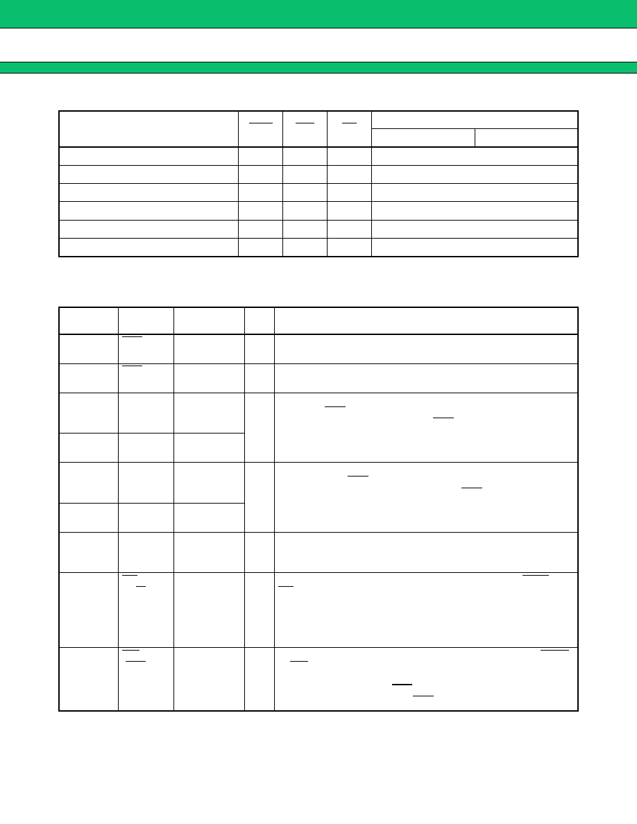
2.
MPU Interface
(Continued)
Phase name
MSG
C/D
I/O
Transfer direction
Initiator
Target
Data-out phase
H
H
H
Data-in phase
H
H
L
Command phase
H
L
H
Status phase
H
L
L
Message-out phase
L
L
H
Message-in phase
L
L
L
Pin
number
Symbol*
Pin name
I/O
Function
77
CS0
Chip select 0
I
This is a chip select 0 pin used by MPU to select the SPC as an
I/O device. This is an active-low pin.
80
CS1
Chip select 1
I
This is a chip select 1 pin to select when MPU inputs/outputs the
data on DMA bus through SPC. This is an active-low pin.
98, 97, 96,
95, 94, 93,
92, 91
D15
to
D8
Data 15
to
data 8
I/O
These pins are for the upper byte and parity bit of MPU data bus.
When the CS0 input is valid, these pins serve as I/O ports for the
SPC internal registers. When the CS1 input is valid, these pins
serve as I/O ports for the DMA bus data.
99
UDP
Upper data
parity
89, 88, 87,
86, 85, 84,
83, 82
D7
to
D0
Data 7
to
data 0
I/O
These pins are for the lower byte and parity bit of the MPU data
bus. When the CS0 input is valid, these pins serve as I/O ports
for the SPC internal registers. When the CS1 input is valid, these
pins serve as I/O ports for the DMA bus data.
81
LDP
Lower data
parity
76, 75, 74,
73, 72
A4
to
A0
Address 4
to
address 0
I
These are address input pins to select the SPC internal
registers.
2
RD
(R/W)
Read
(read/write)
I
In the 80-series mode, this is a read signal input pin (IORD or
RD) that MPU reads the SPC. This read signal pin is an active-
low. In the 68-series mode, this pin functions as the control
signal input (R/W) to control the read/write operation to the SPC.
In the read operation, this pin is an active-high. In the write
operation, this pin is an active-low.
1
WR
(LDS)
Write
(lower data
strobe)
I
In the 80-series mode, this pin is a write signal input pin (IOWR
or WR) that MPU writes to the SPC. This write signal input pin is
active-low. In the 68-series mode, this pin function as the lower
data strobe signal input (LDS) that MPU outputs when the lower
byte of data bus is valid. The LDS pin is an active-low.