DS04-22420-3E
FUJITSU SEMICONDUCTOR
DATA SHEET
ASSP Communication Control
CMOS
FAST-20 SCSI Protocol Controller
MB86606A
s
DESCRIPTION
The MB86606A is an intelligent SCSI protocol controller (SPC) conforming to the ANSI (FAST-20) standard
and integrating a PCI local bus interface function. The specification of SCSI controller block is based on the
MB86605's one which is a Wide SCSI protocol controller, but the device functions/features to achieve the
FAST-20 data transfer rate of maximum 40 Mbyte/sec at 16-bit FAST-20 SCSI, such as the size of internal data
register FIFO, are larged on the MB86606A. As for the SCSI bus pins, a totem pole type single-ended driver/
receiver is incorporated in the device so that it can drive the SCSI bus directly. Furthermore, the MB86606A is
capable of connecting the external differential type driver/receiver.
The SCSI bus sequence is controlled by commands issued via the system interface. So, it supports sequential
commands that perform the phase-to-phase sequences to reduce the overhead of system's sequence
operations.
As another key feature to reduce the system overhead, the device has a 2 Kbytes user program memory to store
the user program with the commands. Due to this, all the SCSI bus sequences including the data transfer can
be performed automatically.
As the system interface block, it incorporates a 32-bit PCI local bus interface that easily realizes the SCSI
interface on the motherboards of PCI bus based PCs and WSs, in addition to a 16-bit separate MPU and DMA
buses. For the on-chip PCI bus interface, the MB86606A also incorporates a 32-bit DMA controller that is capable
of supporting the scatter-gather function so that the data transfers can be controlled by both user program and
the host system.
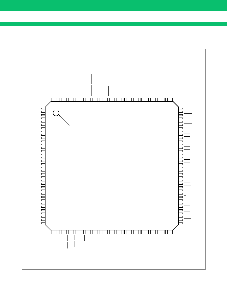
The device is fabricated by the advanced CMOS process and is housed in an 144-pin plastic Quad Flat Package
(Suffix: -PMT2).
s
PACKAGE
(FPT-144P-M08)
144 pin plastic LQFP

2
MB86606A
s
FEATURES
SCSI Protocol Controller Block:
� Operable as initiator and target
� WIDE and FAST-20 data transfers
Synchronous transfer (max. 40 Mbytes/s: Up to 256 offset values can be set.)
Asynchronous transfer (max. 10 Mbytes/s)
� 512-byte FIFO register for data phase
� Two types (send-only and receive-only) of 32-byte data buffers for message, command, and status phases
(MCS Buffers)
� On-chip totem pole type SCSI single-ended driver/receiver
� Supports external SCSI differential driver/receiver connectivity
� On-chip memory to store transfer parameters for each ID (up to 15 connected devices)
� On-chip 16-bit transfer block counter and 24-bit transfer byte counter
Maximum Transfer Byte
: 1 Tbyte at fixed length data transfer
: 16 Mbyte at variable length data transfer
� Supports various control commands:
Sequential Commands
: can perform phase-to-phase sequential operations (functions only when issuing
from a system side.)
Discrete Commands
: can perform any desired sequence to program in the user program memory
Data Transfer Commands : can program the transfer data length at the user program operation.
� On-chip direct control register for SCAM (SCSI Configured AutoMatically) Level-1 Protocol
� Supports Multi Selection/Reselection Responses
Selection and Reselection responses can be done to plural IDs.
� On-chip 2 Kbyte User Program Memory
Two Modes : 2 Kbyte
�
1 bank and 1 Kbyte
�
2 banks
(While 1 Kbyte
�
2 banks are selected, host system can access another bank even if the user
program is executing.)
Access to User program
: Burst transfer via I/O access port
: Direct access to 2 Kbyte user program memory (only for PCI bus I/F mode)
� User Selectable Interrupt Report
Unnecessary interrupt reports can be disabled depending on user's applications to reduce a system ISR
overhead.
� Two automatic receive modes
Initiator : can automatically receive information for new phase to which target switched
Target
: can automatically receive attention condition generated by initiator
� Automatic selection/reselection
For command issues
: automatically performs to receive MSG/CMD to the selection/reselection
request from partner device
For user program operation
: pauses the program currently executed and automatically jumps to the
specified selection /reselection routine in response to the selection/reselection
request from partner device.
� Operation Clock
System Clock: Max. 40 MHz
Internal Processor Operating Clock: Max. 20 MHz
(Continued)

3
MB86606A
(Continued)
System Interface Block:
� Separate MPU and DMA buses called 16-bit Bus Mode
Directly connectable to 68-series or 80-series MPU
Two transfer modes (Program transfer and DMA transfer (slave mode))
� PCI Bus Interface Mode
Directly connectable to the 32-bit PCI local bus.
On-chip 32-bit DMAC for PCI bus master
Supports the PERR&SERR function
Supports the INTA# Interrupt Signals
Max. 64 bytes burst transfer
PCI system clock: Max. 33 MHz
� Data Bus Parity and Address Bus Parity (only for PCI bus interface mode) generation/check function
Others
� Compact 144-Pin Plastic Quad Flat Package (LQFP, Package Suffix: �PMT2)
� Pin compatible with MB86605
� Supply Voltage: 5V
�
5%