 | –≠–ª–µ–∫—Ç—Ä–æ–Ω–Ω—ã–π –∫–æ–º–ø–æ–Ω–µ–Ω—Ç: MB86626 | –°–∫–∞—á–∞—Ç—å:  PDF PDF  ZIP ZIP |
MB86626
Copyright © 2002 Fujitsu Microelectronics Europe GmbH
Page 1 of 6
Disclaimer: The contents of this document are subject to change without notice. Customers are advised to consult with FUJITSU sales representatives before
ordering.The information and circuit diagrams in this document are presented "as is", no license is granted by implication or otherwise.
Product Flyer
January 2002
Version 1.2
FME/MS/ADSLAFE/FL_1/4282
KeyWaveTMAFE ADSL Analog Front End
Mixed Signal Division
ORDERING INFORMATION
Part
Order Number
MB86626 Datasheet
Contact Sales
MB86626 KeyWaveTMAFE
MB86626PFV
MB86626 Development Kit
DK86626-2
DK86626-2 Development
Kit User Manual
Contact Sales
The Fujitsu MB86626 KeyWaveTMAFE ADSL Analog Front End
is a complete analog front end for ADSL modems. The device
integrates high resolution analog to digital converters (ADC)
and digital to analog converters (DAC), and combined with
active filtering significantly reduces the requirements placed on
external components. The architecture supports both analog
and
digital
echo
cancellation
(EC).
The
MB86626
KeyWaveTMAFE is ideal for cost sensitive Remote Terminal
(RT) and power sensitive Central Office (CO) equipment.
FEATURES
∑ Integrates all active circuits except transmit line driver
∑ Programmable for G.dmt (1 channel) or G.lite (2 channel)
∑ Low power, 3.3V operation - from 235mW/ch (2 channel
CO G.lite) to 525mW (RT G.dmt)
∑ Integrated filters and 15-bit A/D & D/A converters
∑ 0 to +38 dB AGC range for receive channel
∑ Supports analog and digital echo cancellation
∑ Excellent SFDR and input noise
∑ 0.35µm CMOS technology with Triple Well
∑ Industrial temperature range (-40 ∞C to +85 ∞C)
APPLICATIONS
∑ ADSL modems
∑ Programmable for several DSL variants
(e.g. G.dmt, G.lite and G.Shdsl)
∑ Single solution for both CO and RT
∑ FDM and echo cancelling systems
∑ Co-exists with ISDN
∑ Analog modem function using second channel (RT G.lite)
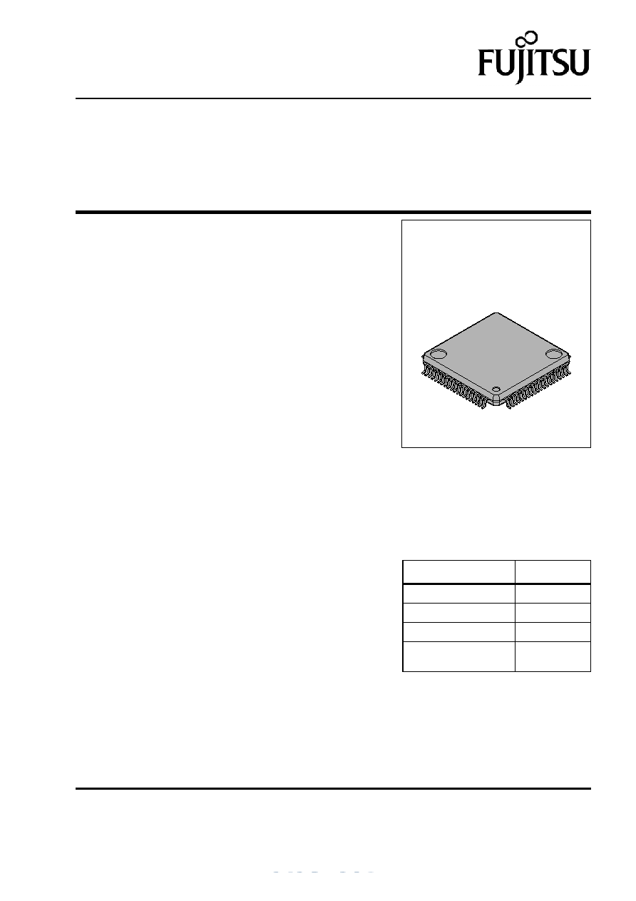
PLASTIC PACKAGE
LQFP-80
January 2002 Version 1.2
FME/MS/ADSLAFE/FL_1/4282
MB86626 KeyWaveTMAFE ADSL Analog Front End
Page 2 of 6
Copyright © 2002 Fujitsu Microelectronics Europe GmbH
Disclaimer: The contents of this document are subject to change without notice. Customers are advised to consult with FUJITSU sales representatives before
ordering.The information and circuit diagrams in this document are presented "as is", no license is granted by implication or otherwise.
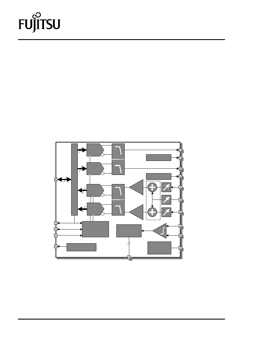
Functional Description
The analog circuitry consists of two 15-bit DACs with associated anti-imaging filters, two 15-bit ADCs
with anti-aliasing filters and two programmable gain summing amplifiers (PGA). A clock multiplier and
bandgap reference are incorporated on-chip. A configurable data interface allows for high speed data
transfer of the receive/transmit data, while a serial interface is provided for control and configuration.
All analog signal paths are differential. This highly integrated device reduces the number of
components required for the line interface to a transmit line driver and a small number of passive
components. Analog echo cancellation at the RT attenuates the transmit echo at the input of the PGA
allowing higher gain before the ADC. This gives lower receiver noise on long lines. A functional block
diagram is shown in Figure 1.
The device is manufactured in a 0.35µm CMOS process with Triple Well extension giving improved
isolation between analog blocks and digital-analog.
Figure 1 KeyWaveTMAFE Functional Block Diagram
PGA
Voltage
Reference
D
a
ta
I
n
te
r
f
a
c
e
16
Tx1
Clk. In
Ext. Ref.
Rx2
Trim
Rx1
Tx2
R/W*
Da
ta
I
n
t
e
r
f
a
c
e
Tx/
E
C/Rx
d
a
ta
VCXO
DAC
Sync.
Serial
Control I/F
4
PAC1
PAC2
PA Control
PA Control
PGA
VCXO Control
DAC
Serial Control
Clock
Generator
15
15
15
15
ADC
ADC
Rx Test P
Rx Test M

January 2002 Version 1.2
FME/MS/ADSLAFE/FL_1/4282
MB86626 KeyWaveTMAFE ADSL Analog Front End
Copyright © 2002 Fujitsu Microelectronics Europe GmbH
Page 3 of 6
Disclaimer: The contents of this document are subject to change without notice. Customers are advised to consult with FUJITSU sales representatives before
ordering.The information and circuit diagrams in this document are presented "as is", no license is granted by implication or otherwise.
Transmit and Receive Channel
The receiver front end has constant resistance programmable attenuators on both receive inputs to
allow for variable line lengths, and to maintain sufficient dynamic range in the programmable gain low
noise summing amplifiers. Anti-aliasing filters are included which have programmable cut-off
frequency and gain control. SNR can be improved by matching the line impedance with the use of
the hybrid balance trim input which reduces echo signals prior to analog/digital echo cancellation
being applied. The ADC uses a proprietary error correcting successive approximation architecture
(patent applied for). In the Central Office the ADC conversion rates are halved compared to Remote
Terminal equipment to reduce power consumption. The attenuators, summing amplifier and filter give
a total gain from input to ADC of 0 to +38dB.
The transmit path features dual DACs and anti-imaging filters with programmable cut-off frequency
and gain. The dual DACs can be configured for oversampling parallel operation for Central Office
use, by internally summing the two Tx outputs. For Remote Terminal the DACs are used
independently for transmit and echo cancellation.
Data and Serial Control Interfaces
Data is transferred to and from the device via a 16-bit data bus. This bus can be configured as either
two byte-wide uni-directional data buses, with one byte for transmit and echo cancellation data and
one byte for receive data, or a single 16-bit bi-directional bus.
The device configuration registers are programmed via a 4-wire serial interface. These registers are
16-bit wide, and are individually accessed using an 8-bit address and control word. Data may be
written to or read from each of these registers.
Clock Multiplier
The device requires a clock source which may be an external reference, or a VCXO which can be
locked to the line symbol rate. The internal clock multiplier generates an internal clock which is then
divided down to provide all required internal and interface clocks. The clock multiplier is a delay line
based design and therefore provides no rejection of input clock jitter.
VCXO Control
The integral VCXO control provides an effective means of controlling an external VCXO clock source.
This digital output uses a first order Sigma-Delta DAC programmed from a 20-bit register. External
RC filtering would normally be provided.
Comparator Function
The KeyWaveTMAFE features a differential comparator which, for example, may be used to detect
whether the telephone on the subscriber line is `on or off hook'.
January 2002 Version 1.2
FME/MS/ADSLAFE/FL_1/4282
MB86626 KeyWaveTMAFE ADSL Analog Front End
Page 4 of 6
Copyright © 2002 Fujitsu Microelectronics Europe GmbH
Disclaimer: The contents of this document are subject to change without notice. Customers are advised to consult with FUJITSU sales representatives before
ordering.The information and circuit diagrams in this document are presented "as is", no license is granted by implication or otherwise.
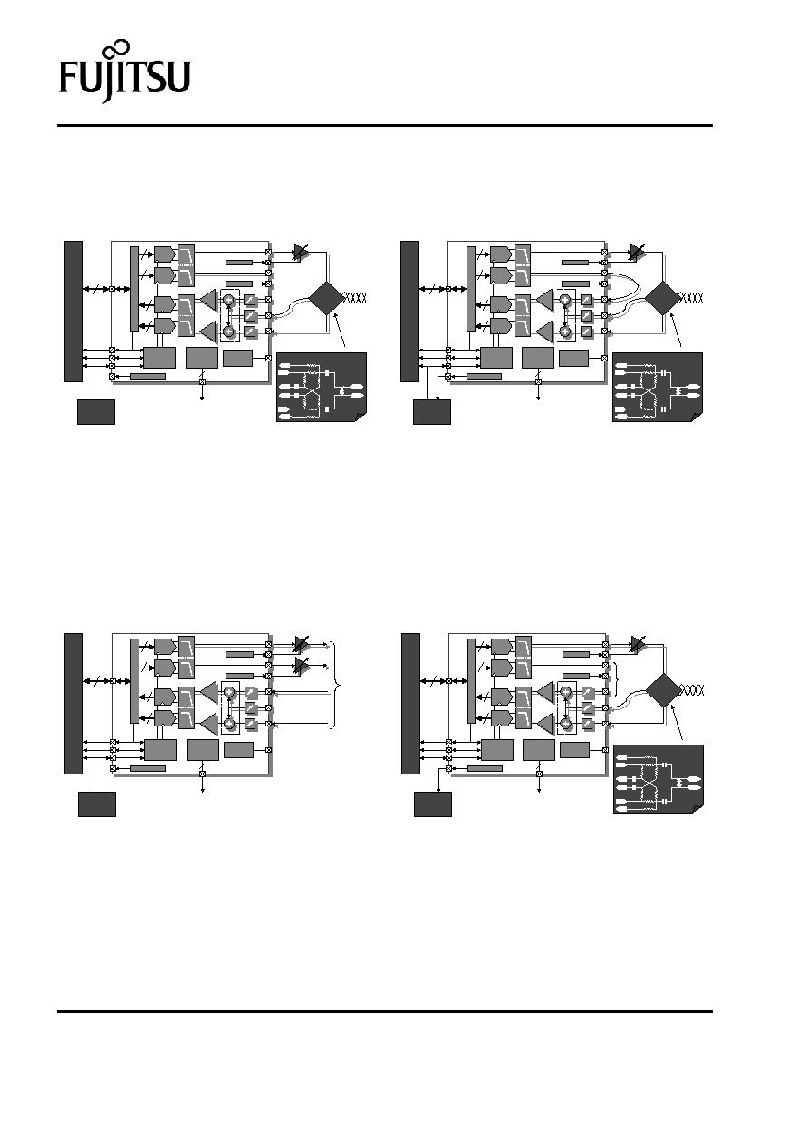
Application Configurations
Figure 2 Full Rate ADSL (G.dmt)
Figure 3 G.lite
Tx
Rx
Trim
Tx/EC
Rx data
Passive
Hybrid
Ref. Clock
17.664MHz
AD
S
L
Mo
d
e
m
Transmit
Line Driver
Twisted
Pair line
PGA
PGA
Voltage
Reference
DAC
Serial
Control I/F
4
PA Control
PA Control
Clock
Generator
D
a
ta
I
n
t
e
r
f
ace
16
15
15
15
15
DAC
ADC
ADC
PGA
PGA
VCXO Control
Simplified Hybrid Circuit
Tx+
Tx-
Rx-
Rx+
Line+
Line-
Trim+
Trim-
Configuration and
control interface
Tx
Rx
Trim
ECin
ECout
Passive
Hybrid
VCXO
17.664MHz
AD
S
L
Mo
d
e
m
Transmit
Line Driver
Twisted
Pair line
PGA
PGA
Voltage
Reference
DAC
Serial
Control I/F
4
PA Control
PA Control
Clock
Generator
D
a
ta
I
n
t
e
r
f
ace
15
15
15
15
DAC
ADC
ADC
PGA
PGA
VCXO Control
Simplified Hybrid Circuit
Tx+
Tx-
Rx-
Rx+
Line+
Line-
Trim+
Trim-
Configuration and
control interface
Tx/EC
Rx data
16
Central Office
Remote Terminal
Tx 1
Rx 1
Rx 2
Ref. Clock
17.664MHz
ADS
L
M
od
e
m
Transmit
Line Drivers
PGA
PGA
Voltage
Reference
DAC
Serial
Control I/F
4
PA Control
PA Control
Clock
Generator
D
a
t
a
I
n
ter
f
ace
15
15
15
15
DAC
ADC
ADC
PGA
PGA
VCXO Control
Configuration and
control interface
Tx 2
Tx/EC
Rx data
16
To
P
assi
ve
H
y
br
i
d
Li
ne
I
n
t
e
r
f
aces
Tx
Rx
Trim
Passive
Hybrid
VCXO
17.664MHz
ADS
L
M
od
e
m
Transmit
Line Driver
Twisted
Pair line
PGA
PGA
Voltage
Reference
DAC
Serial
Control I/F
4
PA Control
PA Control
Clock
Generator
D
a
t
a
I
n
ter
f
ace
15
15
15
15
DAC
ADC
ADC
PGA
PGA
VCXO Control
Simplified Hybrid Circuit
Tx+
Tx-
Rx-
Rx+
Line+
Line-
Trim+
Trim-
Configuration and
control interface
Tx/EC
Rx data
16
Analog Modem
(option)
Central Office (x2)
Remote Terminal
January 2002 Version 1.2
FME/MS/ADSLAFE/FL_1/4282
MB86626 KeyWaveTMAFE ADSL Analog Front End
Copyright © 2002 Fujitsu Microelectronics Europe GmbH
Page 5 of 6
Disclaimer: The contents of this document are subject to change without notice. Customers are advised to consult with FUJITSU sales representatives before
ordering.The information and circuit diagrams in this document are presented "as is", no license is granted by implication or otherwise.
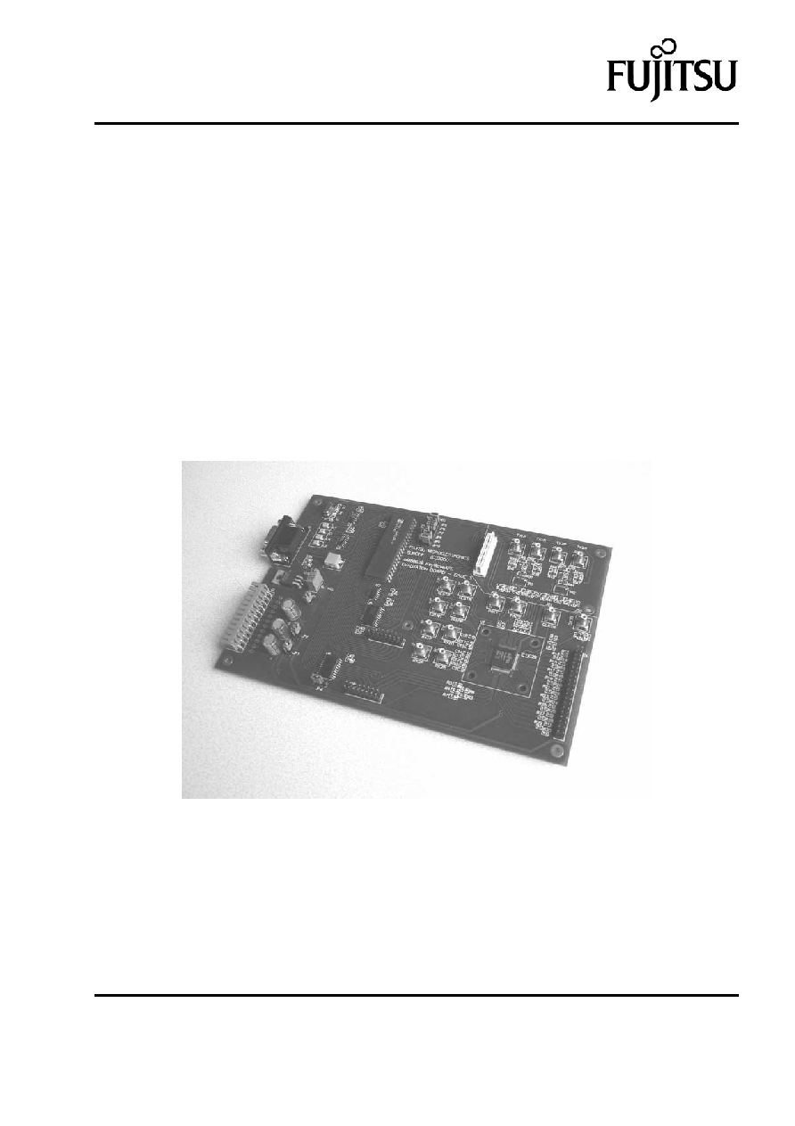
Development Kit
A Development Kit, reference DK86626-2 is available for the MB86626 KeyWaveTMAFE. The board
enables simple and effective evaluation of the device.
The board provides a complete evaluation environment for the KeyWaveTMAFE. Connections for all
analog and digital I/O signals are provided for integration into a target application, and a serial
interface is provided to allow the AFE to be programmed from a host PC. Transmit channel amplifiers
are available, along with a position to plug on a custom hybrid board.
The Development Kit includes,
∑
Evaluation board with MB86626 device fitted
∑
Spare MB86626 for customer development
∑
PC Software for KeyWaveTMAFE register programming
∑
Serial cable, power supply connector and a comprehensive User Manual