 | –≠–ª–µ–∫—Ç—Ä–æ–Ω–Ω—ã–π –∫–æ–º–ø–æ–Ω–µ–Ω—Ç: MB86688B | –°–∫–∞—á–∞—Ç—å:  PDF PDF  ZIP ZIP |
Product Flyer
December 1998
MB86688B
Version 2.0
FireBurstTM25
ATM 25.6 Mbps Multi-PHY Device
FML/NPD/FB25/FL/1126
Copyright © 1998 Fujitsu Microelectronics Limited
Page 1 of 6
The Fujitsu MB86688B FireBurst25 ATM 25.6Mbps Multi-PHY
Device is a highly integrated multiple port interface between the
magnetics and the ATM Adaptation Layer of an ATM system.
Implementing six UNI ports on a single device significantly reduces
the cost per port. Each of the six UNI ports provides framing and
transceiver functions according to the ATM Forum 25.6Mbps
Physical Layer Specification. The device has a 16 bit UTOPIA Level
2 compliant ATM cell interface that can operate at up to 52MHz.
Six 25.6Mbps cell streams are concentrated onto a single Multi-
PHY UTOPIA interface under the control of an ATM Layer device.
Mixed-signal technology is used to implement all the Physical Layer
circuitry at each UNI port. All Physical Media Dependent (PMD)
functions, including line drivers, equalisation and clock recovery are
included in each transceiver block. Transmission Convergence
(TC) functions are performed by each 25.6Mbps framer block.
The FireBurst25 is designed for use in any UTOPIA Level 2 based
system including 622Mbps switches and stand alone concentrators.
Features
∑
Six ATM Forum 25.6Mbps Physical Layer interfaces including all Physical Media Dependent (PMD)
and Transmission Convergence (TC) sub-layer functions
∑
8/16 bit, 52 MHz UTOPIA Level 2 multi-PHY interface with parity
∑
Integrated clock recovery
∑
Digital PLLs - no external filters, no frequency drift, very low recovered clock jitter
∑
HEC generation/detection, discards invalid cells
∑
Maintains statistics on a per UNI port basis
∑
General purpose microprocessor interface (conforms to the UTOPIA Management Interface spec.)
∑
Supports STP and UTP (categories 3, 4, 5)
∑
JTAG compliant to IEEE 1149.1
∑
Fabricated in CMOS technology with CMOS/TTL compatible 5V tolerant I/O and a 3.3V power supply.
∑
-40
∞
C to +85
∞
C Industrial temperature range.
PLASTIC PACKAGE
HQFP-208
December 1998Version 2.0
FML/NPD/FB25/FL/1126
MB86688B FireBurstTM25
Copyright © 1998 Fujitsu Microelectronics Limited
Page 2 of 6
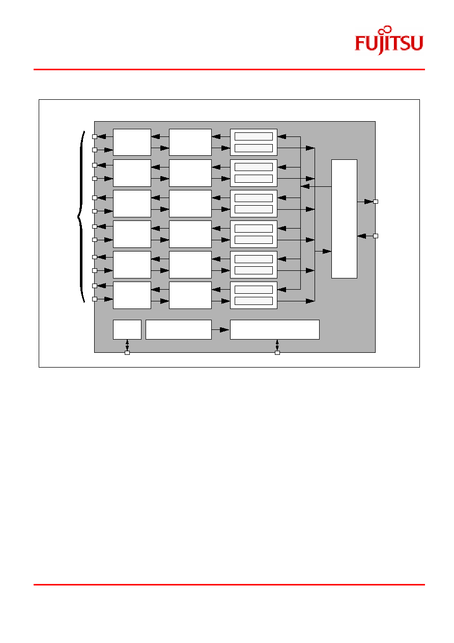
Fig. 1
-
FireBurst25 Block Diagram
General
The Fujitsu MB86688B FireBurst25 provides an interface between six 25.6
Mbps ATM Forum UNI PHY ports and a single UTOPIA Level 2 interface.
Multiple devices can be used in parallel to multiplex a maximum of twenty-four
PHY ports onto a single UTOPIA Level 2 cell stream.
Transceivers
The FireBurst25 has six 25.6Mbps transceivers. Each of these implement all
the Physical Media Dependent (PMD) sub-layer functions for the ATM Forum
25.6Mbps Physical Interface Specification. All Physical Media Dependent
functions, such as transmit line drivers, receiver, equalisation and clock
recovery, are implemented by each transceiver block.
The integrated clock recovery circuitry uses digital PLLs requiring no external
filters. Very low jitter and zero drift is achieved on the recovered clock.
XCVR
Framer
XCVR
Framer
XCVR
Framer
XCVR
Framer
XCVR
Framer
XCVR
Framer
JTAG
Port Statistics
Modules
HOST I/F
UTOPIA
(PMD)
(TC)
(PMD)
(TC)
(PMD)
(TC)
(PMD)
(TC)
(PMD)
(TC)
(PMD)
(TC)
RX Buffer
TX Buffer
RX Buffer
TX Buffer
RX Buffer
TX Buffer
RX Buffer
TX Buffer
RX Buffer
TX Buffer
RX Buffer
TX Buffer
Six UNI
ports
Interface
M-PHY
I/F
Level 2
UTOPIA Management Interface
JTAG Interface
December 1998Version 2.0
FML/NPD/FB25/FL/1126
MB86688B FireBurstTM25
Copyright © 1998 Fujitsu Microelectronics Limited
Page 3 of 6
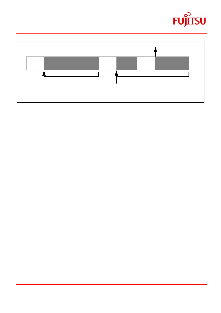
Fig. 2 - ATM Forum 25.6Mbps frame format
Framers
The Transmission Convergence (TC) sub-layer functions specified by the ATM
Forum 25.6Mbps Physical Interface Specification are performed by each of the
six framer blocks.
The structure of a ATM Forum 25.6Mbps frame is shown in Fig. 2. Each framer
interfaces between its associated transceiver and the transmit/receive cell
buffers. Cells for transmission are read from the TX cell buffers, and received
cells (following processing by the framer) are written into the RX cell buffers. The
`X_8' synchronisation event can be used to transfer a global sync pulse
(typically 8kHz).
Statistics Modules
Statistics are generated by each Framer and the Cell Buffer. Counters are
maintained by 6 statistics modules (1 per PHY port). Interrupts may be
generated when a statistics counter requires servicing or the counters may be
read periodically.
Host Interface
The FireBurst25 host interface provides access to all the internal registers and
is used by the device to interrupt the host microprocessor. The interface is
designed to support both Intel and Motorola-compatible microprocessors and is
compliant with the UTOPIA Level 2 Parallel Management Interface guidelines.
Cell Buffers
There are six Cell Buffer modules for each FireBurst25. Each one provides
bidirectional cell synchronisation/buffering between its associated Framer/
Transceiver and the UTOPIA Level 2 (Multi-PHY) interface. Each Cell Buffer
module contains separate transmit and receive storage (giving a total of 12 cell
buffers per device) that buffers up to 3 ATM cells.
X_4
X_X
X_8
SyncEvent
53 Byte ATM Cell
Start of Cell
Start of Cell with
scrambler reset
53 Byte ATM Cell
December 1998Version 2.0
FML/NPD/FB25/FL/1126
MB86688B FireBurstTM25
Copyright © 1998 Fujitsu Microelectronics Limited
Page 4 of 6
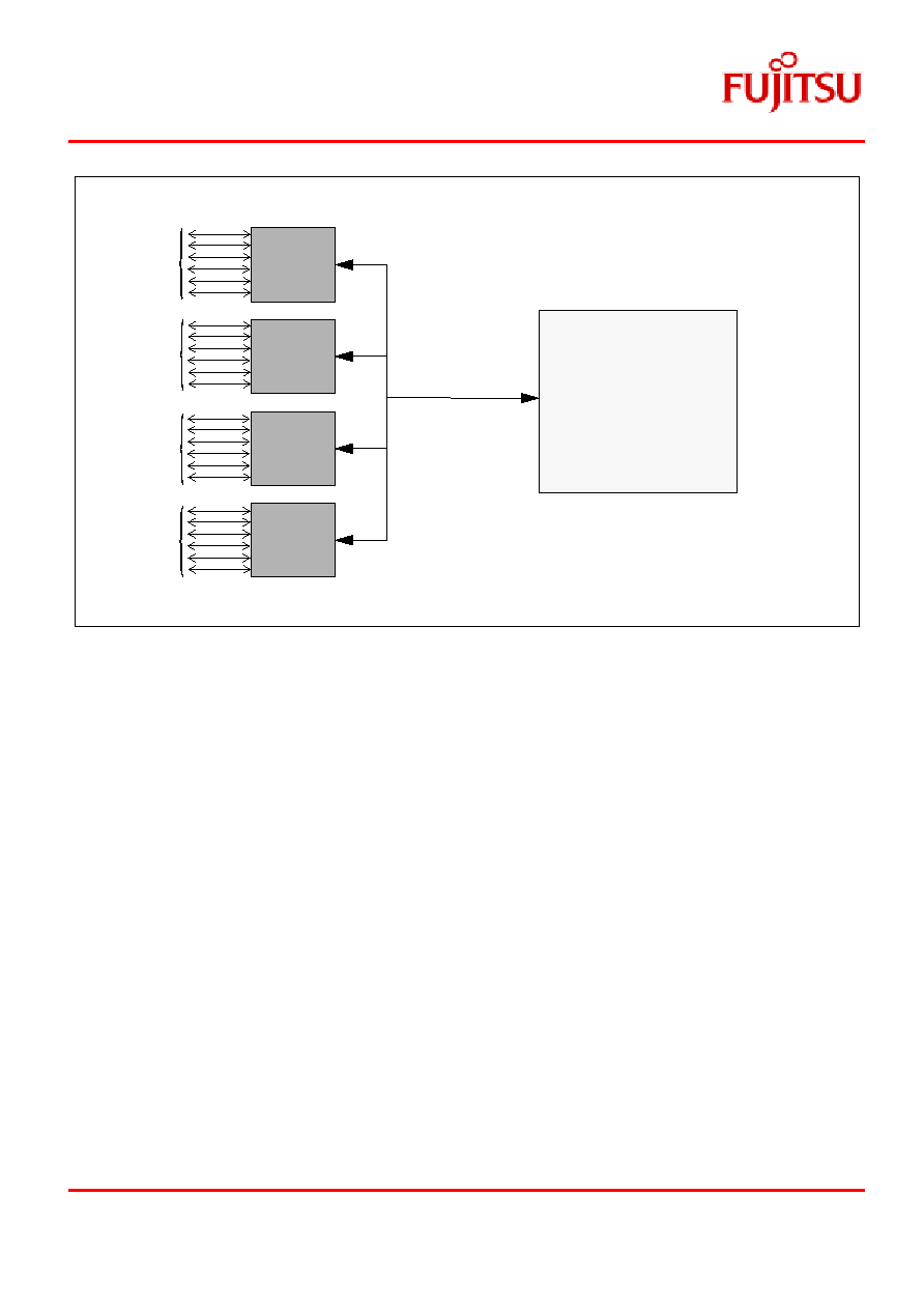
Fig. 3 - Four FireBurst25 devices connected to form a 24 x 25.6 Mbps switch configuration
UTOPIA Level 2 I/F
Cells received from the six UNI ports are transferred to the UTOPIA Level 2
multi-PHY interface under the control of the ATM Layer device. Cells from the
ATM layer are de-multiplexed and can be sent to any of the six UNI ports, also
under control of the ATM Layer device.
Up to four devices can be connected to a single UTOPIA 2 multi-PHY interface.
Fig. 3. shows an example configuration of four FireBurst25 devices connected
via a single 622Mbps Multi-PHY interface to a single ATM layer device forming
a 24 x 25.6 Mbps switch configuration.
JTAG
The FireBurst25 provides boundary scan test circuitry compliant with IEEE
1149.1 (JTAG). This JTAG circuitry permits easier board level testing to be
carried out by allowing the signal pins on the device to form a serial scan chain
around the device. JTAG test modes are controlled by accessing an internal test
access port controller, which is in turn controlled by the 4 provided test access
pins.
FireBurst
25
FireBurst
25
FireBurst
25
FireBurst
25
Switch Fabric
(ATM Layer)
622 Mbps
M-PHY Interface
UTOPIA Level 2
Six UNI
ports
Six UNI
ports
Six UNI
ports
Six UNI
ports
December 1998Version 2.0
FML/NPD/FB25/FL/1126
MB86688B FireBurstTM25
Copyright © 1998 Fujitsu Microelectronics Limited
Page 5 of 6
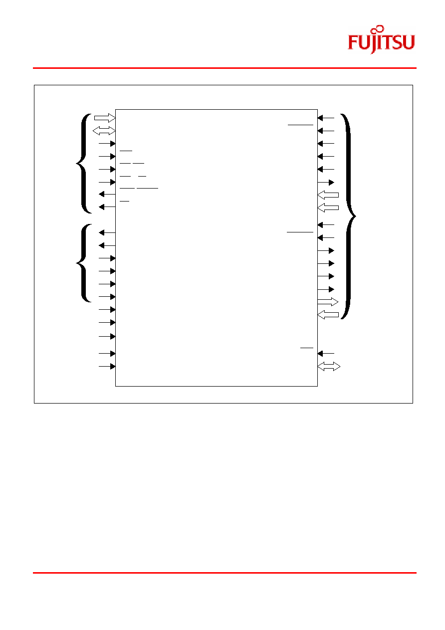
Fig. 4 - MB86688B FireBurst25 I/O Block Diagram
TXClk
TXEnb
TXSOC
TXRef
TXPrty
TXClav
TXData[15:0]
TXAddr[4:0]
RXClk
RXEnb
RXSOC
RXRef
RXPrty
RXClav
RXData[15:0]
RXAddr[4:0]
Addr[7:0]
Data[7:0]
BusMode
Sel
Rd/DS
Wr/RW
RXM(n)
EQM(n)
EQP(n)
CK16M
CK16P
R
ref
V
ref
Rst
JTAG
FireBurst25
Host IF
XCVRS
(x6)
UTOPIA
I/F
Rdy/Dtack
Int
R
HYST
RXP(n)
TXM(n)
TXP(n)