 | –≠–ª–µ–∫—Ç—Ä–æ–Ω–Ω—ã–π –∫–æ–º–ø–æ–Ω–µ–Ω—Ç: MB86941 | –°–∫–∞—á–∞—Ç—å:  PDF PDF  ZIP ZIP |
DS07-05602-5E
FUJITSU SEMICONDUCTOR
DATA SHEET
Microprocessor SPARClite
CMOS
Peripheral LSI for SPARClite
MB86941/942
s
DESCRIPTION
MB86941 and MB86942 are dedicated peripheral LSIs for SPARClite*.
The MB86941 and MB86942 are designed to enable compact configuration of high-performance systems with
SPARClite architecture, and provide the following features.
* : SPARC is a registered trademark of SPARC International base on technology developed by Sun Microsystems,
Inc. SPARClite is a trademark of SPARC International, Inc. licensed exclusively to Fujitsu Microelectronics, Inc.
s
FEATURES
Direct connection to SPARClite
Register read/write in 2 clock cycles up to 30MHz.
Register read/write in 3 clock cycles at 40MHz (MB86941) or 50MHz (MB86942).
Built-In On-Chip Modules:
∑ Interrupt controller
Interrupt input: 15 channels
Each interrupt input has independent masking and trigger mode settings
∑ 16-bit timer: 4 channels
Two of the four channels have prescalers
Each channel has five independent mode operations
MODE0 : Periodical-interrupt
MODE1 : Timeout-interrupt
MODE2 : Square wave generator
(Continued)
s
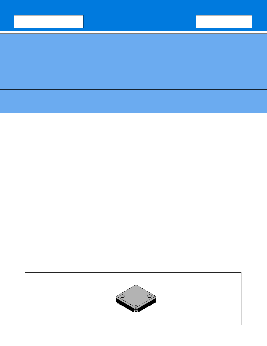
PACKAGE
144-pin Plastic QFP
(FPT-144P-M03)

2
MB86941/942
(Continued)
MODE3: Programmable one shot (software trigger)
MODE4: Programmable one shot (external trigger)
∑ SDTR (Serial data transmitter receiver): 2 channels
MB89251A type
∑ Timing control, CS expansion
Generates read, write and data strobe signals according to the requirements of external devices.
∑ SIO (Synchronous serial input/output)
Simple synchronous type serial input/output
∑ I/O port, 16-bit
Individual direction control by bit
5V single power supply (MB86941), 3.3V single power supply (MB86942)
Upward pin compatibility with MB86940C
3
MB86941/942
s
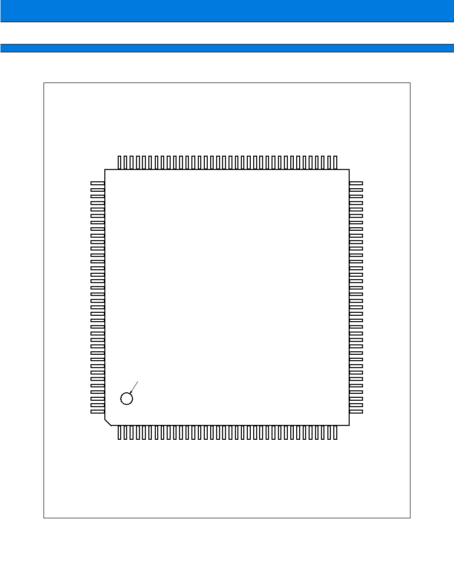
PIN ASSIGNMENT
* : Only for MB86941. Open for MB86942.
SIRXD
SITXD
SIIRQ
N.C.
WSEL
SICLK
N.C.
N.C.
V
SS
RESET#
CLOCK
AS#
RD/WR#
CS#
N.C.
D8
D9
V
DD
V
SS
D10
D11
RS4
RS3
RS2
RS5
RS1
RS0
D12
D13
V
SS
D14
D15
IRQ15
IRQ14
IRQ13
IRQ12
V
DD
IRQ1
1
IRQ10
IRQ9
IRQ8
IRQ7
IRL3
IRL2
V
SS
IRL1
IRL0
IRQ6
IRQ5
IRQ4
IRQ3
CS
0#
RE
ADY
2
#*
V
DD
V
SS
RE
ADY
1
#
CS
1#
IRQ2
IRQ1
CS
2#
CS
3#
DS
R0#
CT
S0#
RT
S
0
#
TRNDT0
V
SS
DT
R0#
SYBRK0
TRDY0
RCLK0
RE
#
WE#
N.C.
IP
D15
IP
D14
IP
D13
IP
D12
IP
D1
1
V
SS
D7
D6
IP
D10
IP
D9
N.C.
IP
D8
IP
D7
IP
D6
D5
D4
V
SS
V
DD
D3
D2
IP
D5
IP
D4
IP
D3
IP
D2
D1
D0
V
SS
OUT3
OUT2
IP
D1
IN2
CLK2
IN3
CLK3
V
DD
IPD0
CLK1
IN1
ACK1
PRSCK1
OUT1
V
SS
OUT0
PRSCK0
ACK0
IN0
CLK0
DSR1#
CTS1#
RTS1#
TRNDT1
DTR1#
V
SS
V
DD
SYBRK1
TRDY1
RCLK1
RCVDT1
RDYOUT#
TCLK1#
DS#
TEMP1
V
SS
RRDY1
RRDY0
TEMP0
TCLK0#
RCVDT0
A1
A0
RCS#
(TOP VIEW)
INDEX
(FPT-144P-M03)
109
110
111
112
113
114
115
116
117
118
119
120
121
122
123
124
125
126
127
128
129
130
131
132
133
134
135
136
137
138
139
140
141
142
143
144
72
71
70
69
68
67
66
65
64
63
62
61
60
59
58
57
56
55
54
53
52
51
50
49
48
47
46
45
44
43
42
41
40
39
38
37
108
107
106
105
104
103
102
101
100
99
98
97
96
95
94
93
92
91
90
89
88
87
86
85
84
83
82
81
80
79
78
77
76
75
74
73
1
2
3
4
5
6
7
8
9
10
11
12
13
14
15
16
17
18
19
20
21
22
23
24
25
26
27
28
29
30
31
32
33
34
35
36
4
MB86941/942
s
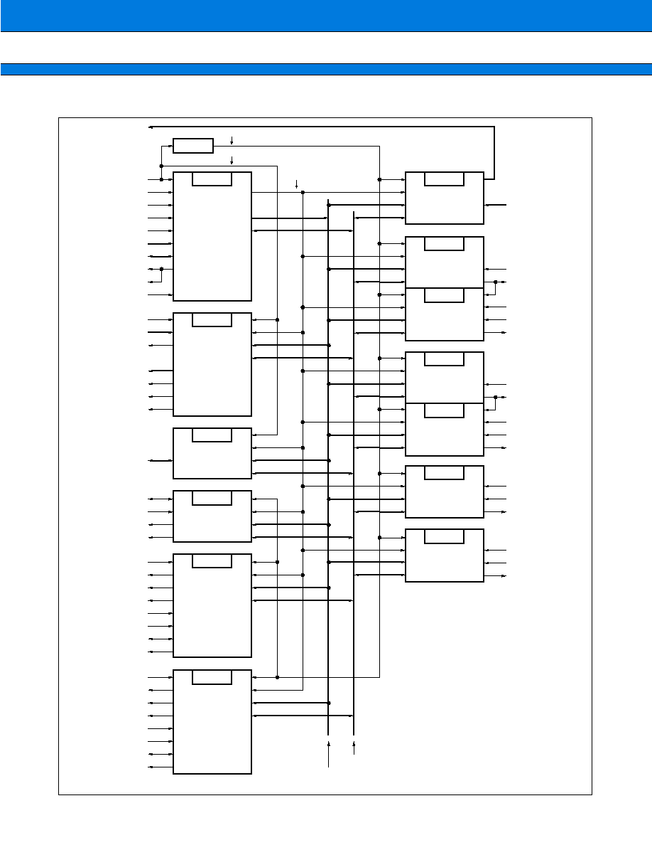
BLOCK DIAGRAM
* : Only for MB86941. Open for MB86942.
CS0# to CS3#
RE#
WE#
DS#
Internal Data Bus
IRL < 3 : 0 >
CLOCK
RESET#
AS#
RD/WR#
CS#
RS < 5 : 0 >
D < 15 : 0 >
READY1#
READY2#*
WSEL
RCS#
A < 1 : 0 >
RDYOUT#
IPD < 15 : 0 >
SICLK
SIRXD
SITXD
SIIRQ
DSR0#, CTS0#
RTS0#, DTR0#
TEMP0, TRDY0
TRNDT0
TCLK0#
RCLK0, RCVDT0
SYBRK0
RRDY0
DSR1#, CTS1#
RTS1#, DTR1#
TEMP1, TRDY1
TRNDT1
TCLK1#
RCLK1, RCVDT1
SYBRK1
RRDY1
˜
2
BIU
1 / 2 Clock
1 / 1 Clock
Bus
Interface
Unit
RCSTG
Read/Write
Chip Select
Timing
Generator
IP
SIO
SDTR0
SDTR1
I/O Port
Serial Data
Input
Output
Serial Data
Transmitter
Receiver
Serial Data
Transmitter
Receiver
Reset
IRC
PRS0
TM0
PRS1
TM1
TM2
TM3
Interrupt
Request
Controller
Prescaler
Prescaler
Timer
Timer
Timer
Timer
Internal Control Bus
IRQ1 to IRQ15
ACK0
PRSCK0
CLK0
IN0
OUT0
ACK1
PRSCK1
CLK1
IN1
OUT1
CLK2
IN2
OUT2
CLK3
IN3
OUT3

5
MB86941/942
s
DESCRIPTION OF BLOCK FUNCTIONS
1. BIU (Bus Interface Unit)
This block receives MPU (SPARClite) bus signals and bus controls signals (CLOCK, AS#, RD/WR#, CS#, ADR6
to ADR2, D<15:0>) and generates control signals for accessing MB86941/MB86942 internal resources. It also
returns that Ready signal to the MPU which corresponds to the access time of each of such resources.
2. IRC (Interrupt Request Controller)
This block provides 15-channel interrupt input signals to transmit the interrupt level IRL <3:0> for each interrupt
to the SPARClite.
3. TM (Timer) and PRS (Prescaler)
TM0 to TM3 are 16-bit timers serving as periodic interrupt generation timers, a watchdog timer, and an external
event counter. The operating clock can be selected from among the internal clock, the clock frequency-divided
by the prescaler, and the external clock.
Prescalers 0 and 1 are linked with timer channels 0 and 1, respectively. Each of the prescalers is initialized upon
loading (or reloading) of the timer initial value of the corresponding timer.
4. SDTR (Serial Data Transmitter Receiver)
SDTR0 and SDTR1 are serial data transmitter/receiver modules programmable for control of transmission and
reception.
The programming model is the same as that for the MB89251A.
5. RCSTG (Read/Write Timing Generator)
This module generates read, write, and data strobe signals conforming to the required timings for external
connection of other devices. The assert timing and pulse width of each signal to be generated is programmable.
6. IP (I/O Port)
There are 16 I/O ports. The input/output direction of each port can be set by the control register.
7. SIO (Serial Data Input Output)
This block is a clock-synchronous serial interface. The transfer clock signal can be set to the internally generated
or externally input one. The SIO outputs data to be transmitted and inputs received data in synchronization with
the transfer clock signal.