
DS04-29120-1E
FUJITSU SEMICONDUCTOR
DATA SHEET
Spread Spectrum Clock Generator
MB88156
DESCRIPTION
MB88156 is a clock generator for EMI (Electro Magnetic Interference) reduction. The peak of unnecessary radi-
ation noise (EMI) can be attenuated by making the oscillation frequency slightly modulate periodically with the
internal modulator. The modulation corresponds to the center spread and down spread. The multiplication ratio
can be changed by the pin setting.
Also, the pin can be set whether the modulation is changed. For no modulation, it has the center-non-spread to
fix to the output frequency conforming to the multiplication setting and down-non-spread to fix the output frequency
to center frequency of the down spread.
FEATURES
∑ Input frequency :
12.5 MHz to 50 MHz (multiplied by 1)
12.5 MHz to 25 MHz (multiplied by 2)
12.5 MHz to 20 MHz (multiplied by 4)
∑ Output frequency :
CKOUT 12.5 MHz to 80 MHz
REFOUT the same as input frequency (not multiplied)
(Continued)
PACKAGE
16-pin plastic BCC
(LCC-16P-M09)
MB88156
2
(Continued)
∑ Modulation rate
:
±
0.5
%
,
±
1.0
%
(center spread) ,
-
1.0
%
,
-
2.0
%
(down spread)
∑ Frequency down function
:
-
0.5
%
,
-
1.0
%
(for down-non-spread)
∑ Equipped with oscillation circuit
: Oscillation range 12.5 MHz to 40 MHz (Fundamental oscillation mode)
40 MHz to 48 MHz (At 3rd over tone)
∑ Modulation clock output Duty
: 40
%
to 60
%
∑ Modulation clock Cycle-Cycle Jitter : Multiplied by 1 (input) 12.5 MHz to 20 MHz less than 150 ps
Multiplied by 1 (input) 20.0 MHz to 50 MHz less than 100 ps
Multiplied by 2 (input) 12.5 MHz to 25 MHz less than 200 ps
Multiplied by 4 (input) 12.5 MHz to 20 MHz less than 200 ps
∑ Low current consumption by CMOS process : 5 mA (24 MHz : Typ-sample, no load)
∑ Power supply voltage : 3.3 V
±
0.3 V
∑ Operating temperature :
-
40
∞
C to
+
85
∞
C
∑ Package : BCC 16-pin
PRODUCT LINEUP
Product
Function
MB88156-000
With REFOUT
MB88156-001
Without REFOUT
MB88156
3
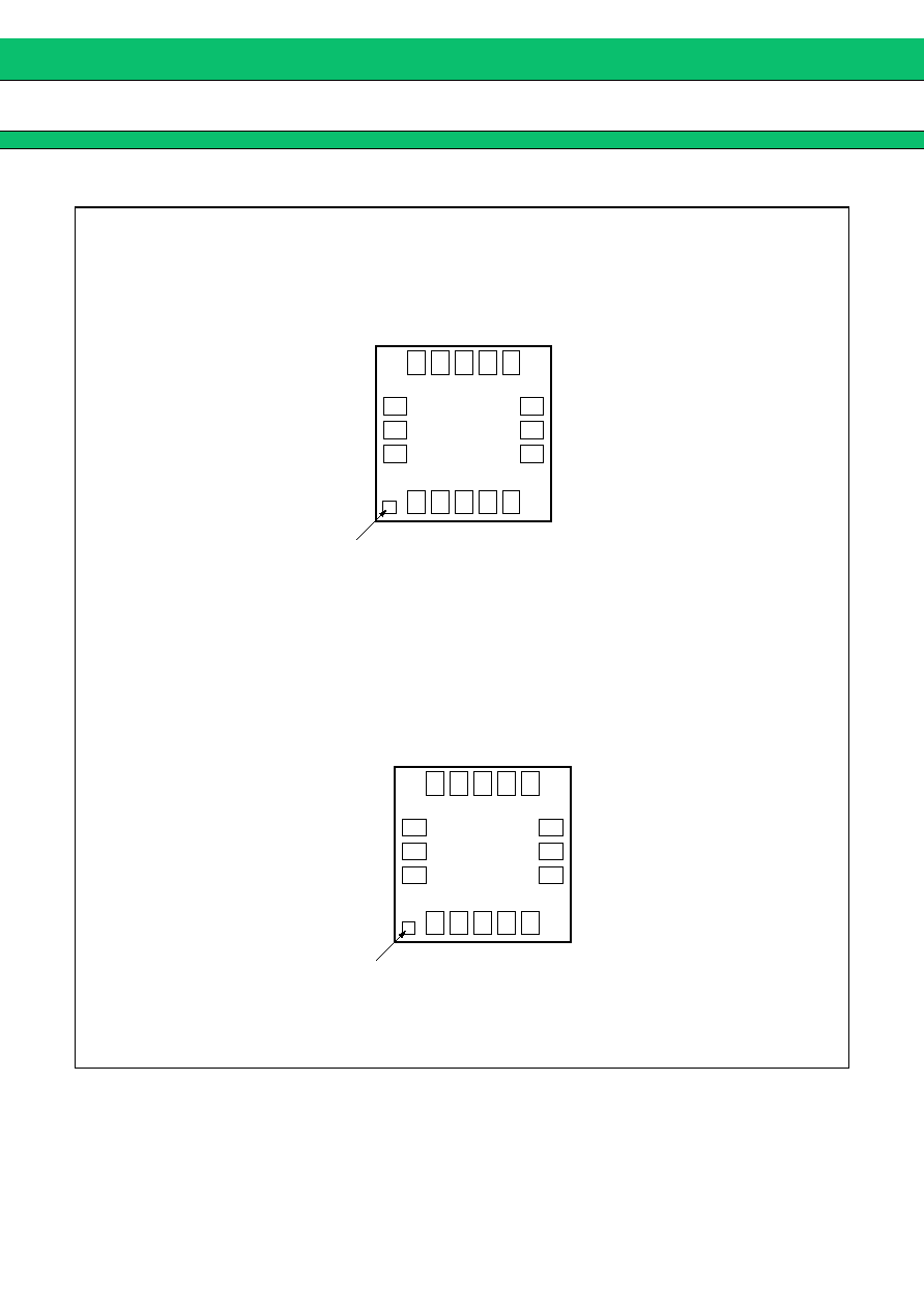
PIN ASSIGNMENT
14
15
16
N.C.
N.C.
N.C.
8
7
6
FREQ
MLTP0
MLTP1
13
1
2
3
4
5
12 11 10
9
SEL
XPD
ENS
XOU
T
XIN
CK
OUT
V
SS
SPRD
R
EFOUT
V
DD
index
MB88156
-000
14
15
16
N.C.
N.C.
N.C.
8
7
6
FREQ
MLTP0
MLTP1
13
1
2
3
4
5
12 11 10
9
SEL
XPD
ENS
XOU
T
XIN
C
K
OUT
V
SS
SPRD
N.C
.
V
DD
index
MB88156
-001
TOP VIEW
TOP VIEW
∑
MB88156-000
∑
MB88156-001
LCC-16P-M09
MB88156
4
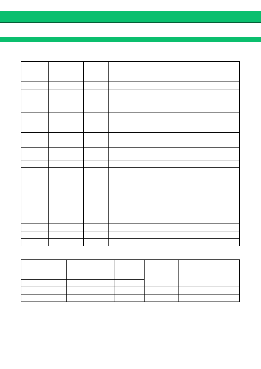
PIN DESCRIPTION
∑
Setting of MLTP1, MLTP0, and FREQ (Setting of multiplication rate and input frequency)
Note : Setting other than above is disabled.
Pin no.
Pin name
I/O
Description
1
CKOUT
O
Modulated clock output pin
Output "L" at power-down
2
V
SS
GND pin
3
SPRD
I
Modulation type setting pin/frequency down setting
SPRD
=
"L" : Down spread/down-non-spread
SPRD
=
"H" : Center spread/center-non-spread
For details, see "Setting of ENS, SPRD, and SEL".
4
REFOUT/N.C.
O
Non modulation clock output pin (output "L" at power-down) /non
connection pin
5
V
DD
Power supply voltage pin
6
MLTP1
I
Multiplication rate setting pin
For details, see "Setting of MLTP1, MLTP0, and FREQ".
7
MLTP0
I
8
FREQ
I
Frequency setting pin
For details, see "Setting of MLTP1, MLTP0, and FREQ".
9
XIN
I
Pin for the connection of resonator/clock input
10
XOUT
O
Connecting pin of resonator
11
ENS
I
Modulation enable setting pin
ENS
=
"L" : Non modulation
ENS
=
"H" : Modulation
12
XPD
I
Power down pin
XPD
=
"L" : Power down
XPD
=
"H" : Normal operation
13
SEL
I
Modulation rate setting pin/frequency falling width setting pin
For details, see "Setting of ENS, SPRD, and SEL".
14
N.C.
Non connection pin
15
N.C.
Non connection pin
16
N.C.
Non connection pin
Input frequency
Output frequency
FREQ
Multiplication
rate
MLTP1
MLTP0
12.5 MHz to 25 MHz
12.5 MHz to 25.0 MHz
L
Multiplied by 1
L
L
25.0 MHz to 50 MHz
25.0 MHz to 50.0 MHz
H
12.5 MHz to 25 MHz
25.0 MHz to 50.0 MHz
L
Multiplied by 2
H
L
12.5 MHz to 20 MHz
50.0 MHz to 80.0 MHz
L
Multiplied by 4
H
H
MB88156
5
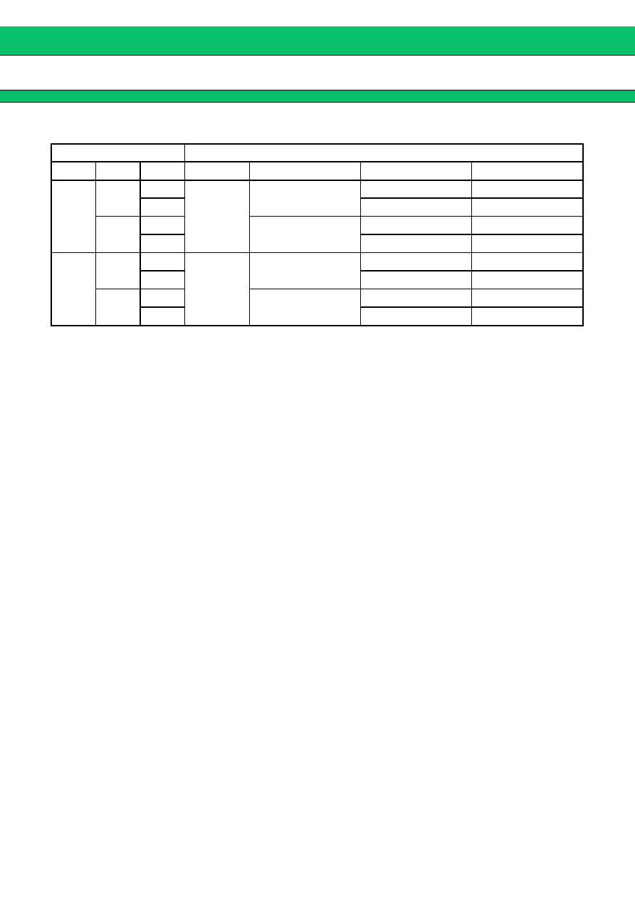
∑
Setting of ENS, SPRD, and SEL (setting of output frequency)
Setting pin
Output status
ENS
SPRD
SEL
Modulation
Modulation type
Modulation rate
Falling width
L
L
L
None
Down-non-spread
-
0.5
%
H
-
1.0
%
H
L
Center-non-spread
0.0
%
H
0.0
%
H
L
L
Provided
Down spread
-
1.0
%
H
-
2.0
%
H
L
Center spread
±
0.5
%
H
±
1.0
%
MB88156
6
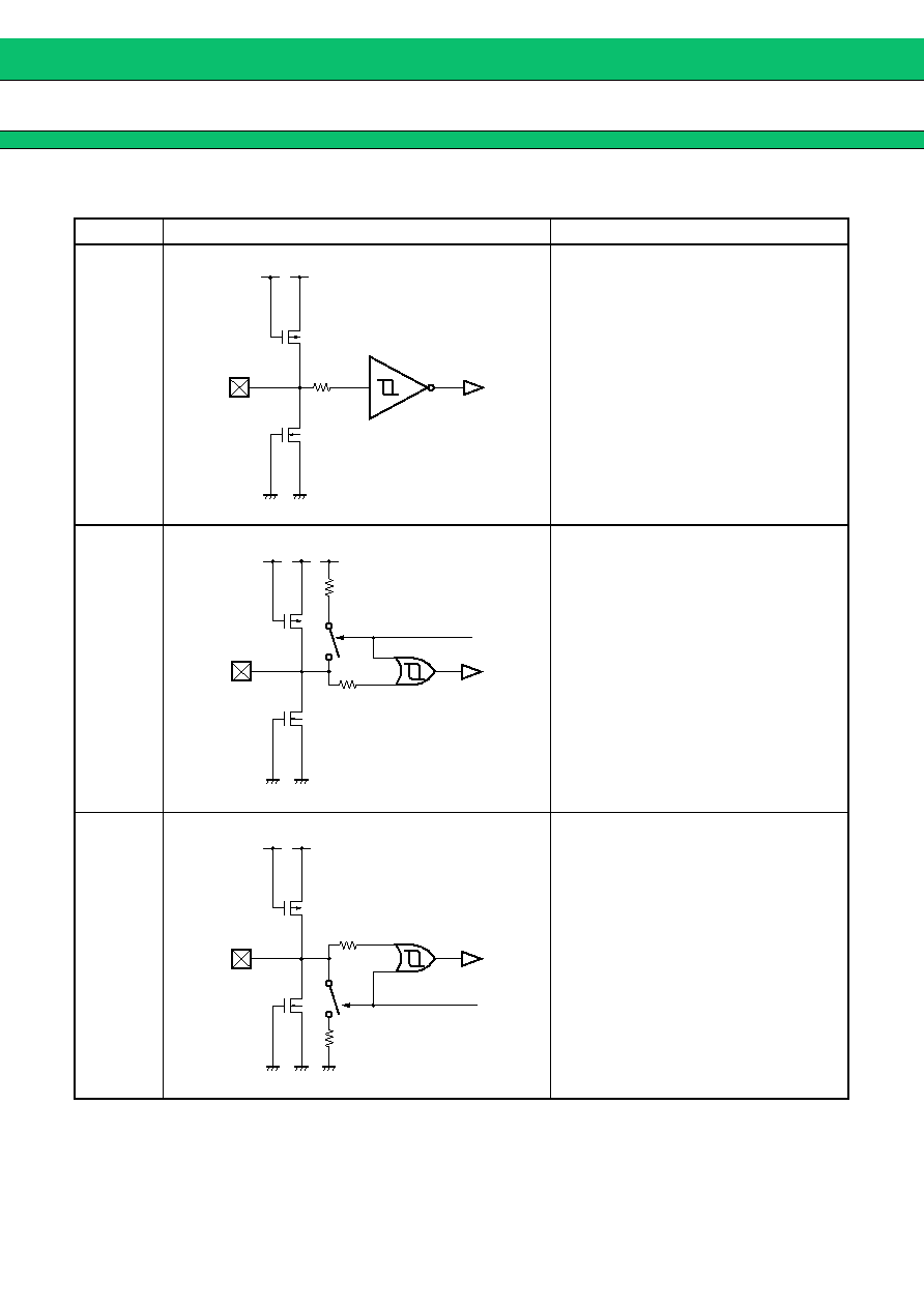
I/O CIRCUIT TYPE
(Continued)
Pin
Circuit type
Remarks
SEL,
XPD
∑ CMOS hysteresis input
ENS,
SPRD
∑ CMOS hysteresis input with pull-up
resistor 50 k
(Typ)
∑ At power-down, pull-up resistance is
shut off.
FREQ,
MLTP1,
MLTP0
∑ CMOS hysteresis input with
pull-down resistor 50 k
(Typ)
∑ At power-down, pull-down resistance
is shut off.
50 k
Power down signal
50 k
Power down signal
MB88156
7
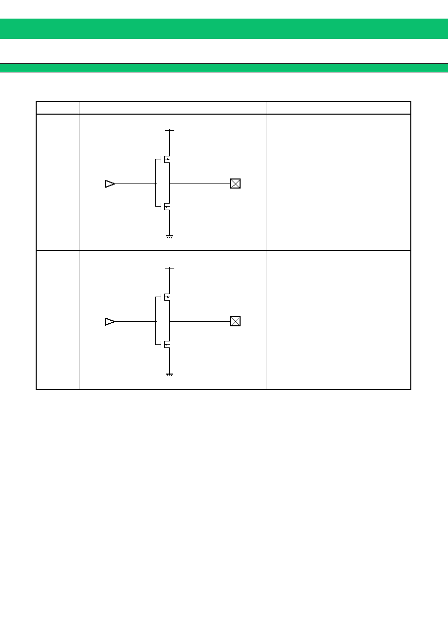
(Continued)
Note : For XIN and XOUT pins, see "
OSCILLATION CIRCUIT".
Pin
Circuit type
Remarks
REFOUT
∑ CMOS output
∑ I
OL
=
3 mA
∑ Output "L" at power-down
CKOUT
∑ CMOS output
∑ I
OL
=
4 mA
∑ Output "L" at power-down

MB88156
8
HANDLING DEVICES
Preventing Latchup
A latchup can occur if, on this device, (a) a voltage higher than V
DD
or a voltage lower than V
SS
is applied to an
input or output pin or (b) a voltage higher than the rating is applied between V
DD
and V
SS
. The latchup, if it occurs,
significantly increases the power supply current and may cause thermal destruction of an element. When you
use this device, be very careful not to exceed the maximum rating.
Handling unused pins
Do not leave an unused input pin open, since it may cause a malfunction. Handle by, using a pull-up or pull-
down resistor.
Unused output pin should be opened.
The attention when the external clock is used
Input the clock to XIN pin, and XOUT pin should be opened when you use the external clock.
Please pay attention so that an overshoot and an undershoot do not occur to an input clock of XIN pin.
Power supply pins
Please design connecting the power supply pin of this device by as low impedance as possible from the current
supply source.
We recommend connecting electrolytic capacitor (about 10
µ
F) and the ceramic capacitor (about 0.01
µ
F) in
parallel between V
SS
and V
DD
near the device, as a bypass capacitor.
Oscillation circuit
Noise near the XIN and XOUT pins may cause the device to malfunction. Design printed circuit boards so that
electric wiring of XIN or XOUT pin and the resonator do not intersect other wiring.
Design the printed circuit board that surrounds the XIN and XOUT pins with ground.
Handling N.C. pin
Be sure to open the N.C. pin when it is used.
MB88156
9
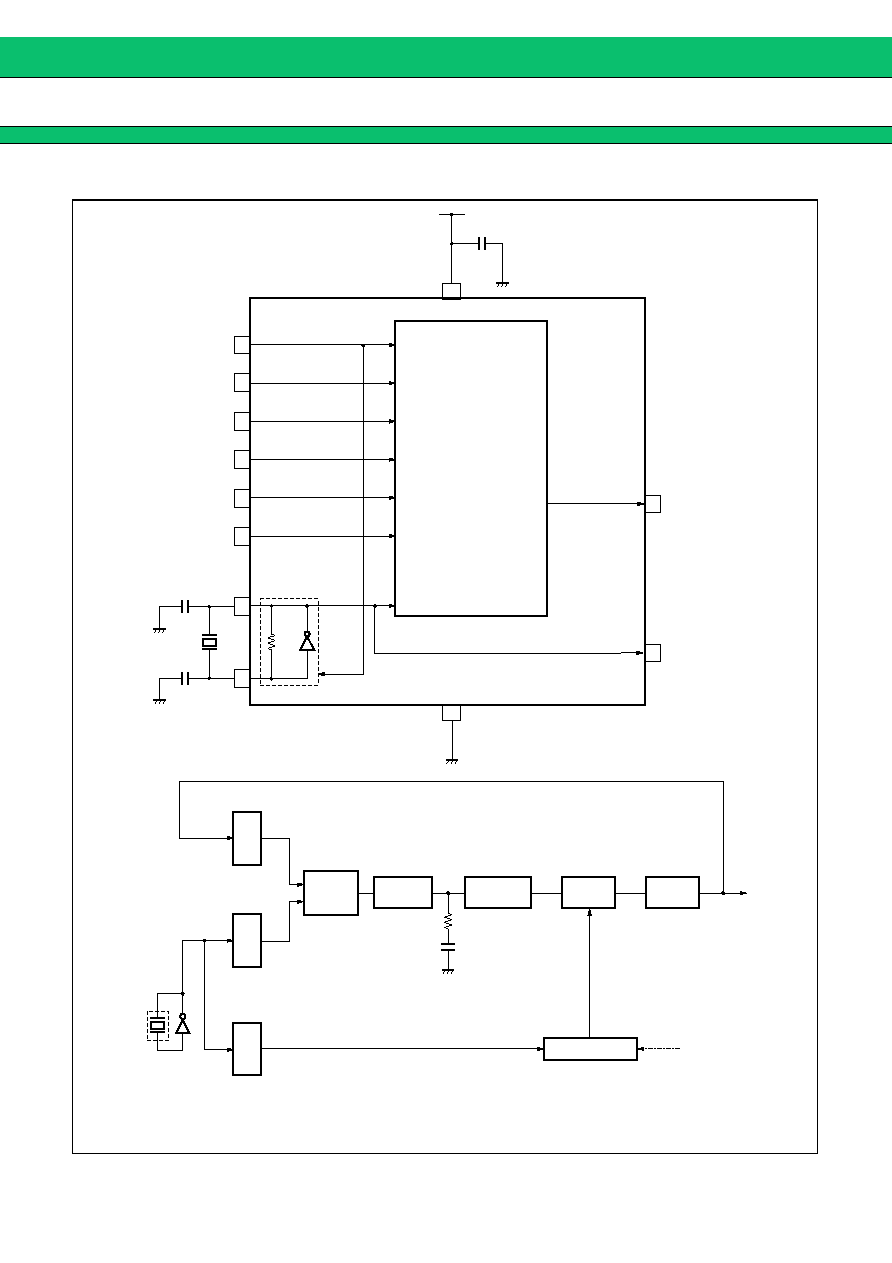
BLOCK DIAGRAM
V
DD
V
SS
CKOUT
REFOUT/N.C.
XPD
SPRD
SEL
XOUT
XIN
R
f
=
1 M
ENS
MLTP1,
MLTP0
FREQ
Reference clock output
Reference clock
Multiplication rate
setting
Power down signal
Frequency setting
Modulation type
setting/frequency
down setting
Modulation enable
setting
Power down
Modulation
clock output
PLL block
Modulation level
setting/frequency
falling width setting
1
-
M
1
-
N
1
-
L
IDAC
ICO
Reference clock
Loop filter
Modulation logic
Modulation
clock output
V/I
conversion
Charge
pump
Phase
compare
SEL
ENS
Modulation level setting/
frequency falling width setting
MB88156 PLL block
A glitchless IDAC (current output D/A converter) provides precise modulation, thereby dramatically
reducing EMI.
MB88156
10
PIN SETTING
After the pin setting is changed, the stabilization wait time of the modulation clock is required. The stabilization
wait time of the modulation clock takes the maximum value of Lock-Up time in "AC Characteristics" in
ELECTRICAL CHARACTERISTICS.
ENS modulation enable/disable setting
Spectrum does not spread when "L" is set to ENS pin.
XPD power down
When setting "L" to XPD pin, it becomes power down mode (low power consumption mode) .
Both of CKOUT and REFOUT for the output pin fixes to "L" output during the power down.
SPRD modulation type setting/frequency down setting
SEL modulation level setting/frequency falling width setting
MLTP1, MLTP0 multiplication rate setting
Note : REFOUT is not multiplied.
FREQ frequency setting
ENS
Modulation
L
No modulation
H
Modulation
XPD
Status
L
Power down status
H
Operating status
SPRD
Status
L
Down spread/down-non-spread
H
Center spread/center-non-spread
SEL
Status
L
±
0.5
%
(at center spread) /
±
0.0
%
(at center-non-spread)
-
1.0
%
(at down spread) /
-
0.5
%
(at down-non-spread)
H
±
1.0
%
(at center spread) /
±
0.0
%
(at center-non-spread)
-
2.0
%
(at down spread) /
-
1.0
%
(at down-non-spread)
MLTP1
MLTP0
Multiplication rate
L
L
Multiplied by 1
H
L
Multiplied by 2
H
H
Multiplied by 4
FREQ
Input frequency
L
12.5 MHz to 25 MHz (Multiplied by 1, 2) /
12.5 MHz to 20 MHz (Multiplied by 4)
H
25 MHz to 50 MHz (Multiplied by 1)

MB88156
11
∑
Center spread
Spectrum is spread (modulated) by centering on the non-spread frequency.
∑
Down spread
Spectrum is spread (modulated) below the non-spread frequency.
∑
Down-non-spread
Slightly lowering the output frequency with modulation stopped fixes it to the center frequency for down spreading.
-
1.0%
+
1.0%
Radiation level
Non-spread frequency
Frequency
Example of center spread modulation rate
±
1.0% (2.0%)
Modulation width 2.0%
-
2.0%
Radiation level
Non-spread frequency
Frequency
Example of down spread modulation rate
-
2.0%
Modulation width 2.0%
-
1.0%
Radiation level
Frequency of multiplication ratio setting
Frequency
Down frequency
Example of down-non-spread
-
1.0%
MB88156
12
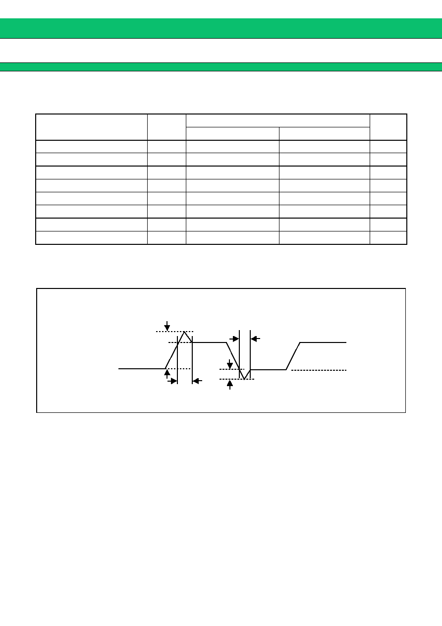
ABSOLUTE MAXIMUM RATINGS
*: The parameter is based on V
SS
=
0.0 V.
WARNING: Semiconductor devices can be permanently damaged by application of stress (voltage, current,
temperature, etc.) in excess of absolute maximum ratings. Do not exceed these ratings.
Parameter
Symbol
Rating
Unit
Min
Max
Power supply voltage*
V
DD
-
0.5
+
4.0
V
Input voltage*
V
I
V
SS
-
0.5
V
DD
+
0.5
V
Output voltage*
V
O
V
SS
-
0.5
V
DD
+
0.5
V
Storage temperature
T
ST
-
55
+
125
∞
C
Operation junction temperature
T
J
-
40
+
125
∞
C
Output current
I
O
-
14
+
14
mA
Overshoot
V
IOVER
V
DD
+
1.0 (t
OVER
50 ns)
V
Undershoot
V
IUNDER
V
SS
-
1.0 (t
UNDER
50 ns)
V
V
DD
V
SS
Input pin
Overshoot/Undershoot
t
UNDER
50 ns
V
IOVER
V
DD
+
1.0 V
t
OVER
50 ns
V
IUNDER
V
SS
-
1.0 V
MB88156
13
RECOMMENDED OPERATING CONDITIONS
(V
SS
=
0.0 V)
WARNING: The recommended operating conditions are required in order to ensure the normal operation of the
semiconductor device. All of the device's electrical characteristics are warranted when the device is
operated within these ranges.
Always use semiconductor devices within their recommended operating condition ranges. Operation
outside these ranges may adversely affect reliability and could result in device failure.
No warranty is made with respect to uses, operating conditions, or combinations not represented on
the data sheet. Users considering application outside the listed conditions are advised to contact their
FUJITSU representatives beforehand.
Parameter
Symbol
Pin
Conditions
Value
Unit
Min
Typ
Max
Power supply voltage
V
DD
V
DD
3.0
3.3
3.6
V
"H" level input voltage
V
IH
XIN, SEL, ENS,
FREQ, MLTP1,
MLTP0, SPRD,
XPD
V
DD
◊
0.8
V
DD
+
0.3
V
"L" level input voltage
V
IL
XIN, SEL, ENS,
FREQ, MLTP1,
MLTP0, SPRD,
XPD
V
SS
V
DD
◊
0.2
V
Input clock duty cycle
t
DCI
XIN
12.5 MHz to 50 MHz
40
50
60
%
Operating temperature
Ta
-
40
+
85
∞
C
XIN
t
a
t
b
1.5 V
Input clock duty cycle (t
DCI
=
t
b
/t
a
)
MB88156
14
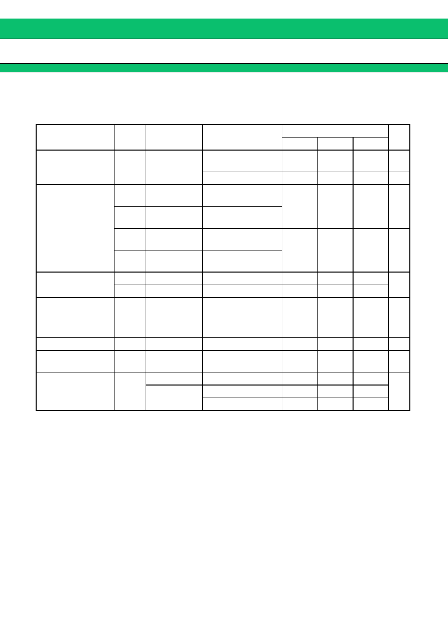
ELECTRICAL CHARACTERISTICS
∑
DC Characteristics
(Ta
=
-
40
∞
C to
+
85
∞
C, V
DD
=
3.3 V
±
0.3 V, V
SS
=
0.0 V)
Parameter
Symbol
Pin
Conditions
Value
Unit
Min
Typ
Max
Power supply current
I
CC
V
DD
24 MHz output
No load capacitance
5.0
7.0
mA
At power-down
10
µ
A
Output voltage
V
OHC
CKOUT
"H" level output
I
OH
=
-
4 mA
V
DD
-
0.5
V
DD
V
V
OHR
REFOUT
"H" level output
I
OH
=
-
3 mA
V
OLC
CKOUT
"L" level output
I
OL
=
4 mA
V
SS
0.4
V
V
OLR
REFOUT
"L" level output
I
OL
=
3 mA
Output impedance
Z
OC
CKOUT
12.5 MHz to 80 MHz
45
Z
OR
REFOUT
12.5 MHz to 50 MHz
70
Input capacitance
C
IN
SEL, ENS,
FREQ, MLTP1,
MLTP0, SPRD,
XPD
Ta
=
+
25
∞
C
V
DD
=
V
I
=
0.0 V
f
=
1 MHz
16
pF
Pull-up resistor
R
PU
ENS, SPRD
25
50
200
k
Pull-down resistor
R
PD
FREQ, MLTP1,
MLTP0
25
50
200
k
Load capacitance
C
L
REFOUT
12.5 MHz to 50 MHz
15
pF
CKOUT
12.5 MHz to 50 MHz
15
50 MHz to 80 MHz
7
MB88156
15
∑
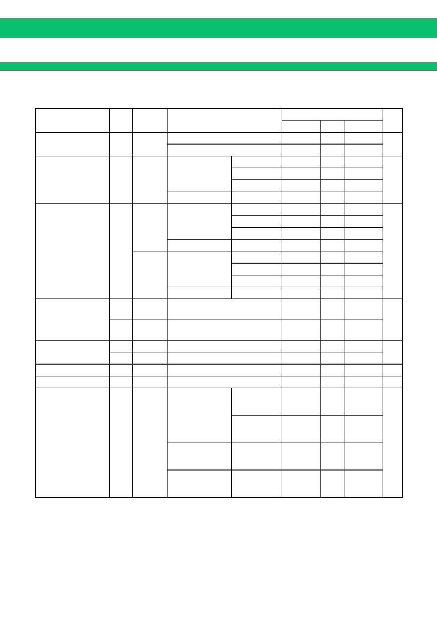
AC Characteristics
(Ta
=
-
40
∞
C to
+
85
∞
C, V
DD
=
3.3 V
±
0.3 V, V
SS
=
0.0 V)
*1 : Because the duty of REFOUT pin output depends on t
DCI
of the input clock duty, it is assured only when either
A or B condition is used as follow:
A : Resonator input : When the resonator is connected to the XIN pin and XOUT pin and oscillates normally.
B : External clock input : The input level is full swing (V
SS
-
V
DD
) .
*2 : After power on and release of power down or changing the pin setting (SEL, ENS, FREQ, MLTP1 and MLTP0,
and SPRD) , the stabilization wait time of the modulation clock is required. The stabilization wait time of the
modulation clock takes the maximum value of Lock-Up time.
Parameter
Sym-
bol
Pin
Conditions
Value
Unit
Min
Typ
Max
Oscillation frequency
f
x
XIN,
XOUT
Fundamental oscillation
12.5
40
MHz
3rd overtone
40
48
Input frequency
f
in
XIN
FREQ
=
0
Multiplied by 1
12.5
25
MHz
Multiplied by 2
12.5
25
Multiplied by 4
12.5
20
FREQ
=
1
Multiplied by 1
25
50
Output frequency
f
OUT
REFOUT
FREQ
=
0
Multiplied by 1
12.5
25
MHz
Multiplied by 2
12.5
25
Multiplied by 4
12.5
20
FREQ
=
1
Multiplied by 1
25
50
CKOUT
FREQ
=
0
Multiplied by 1
12.5
25
Multiplied by 2
25
50
Multiplied by 4
50
80
FREQ
=
1
Multiplied by 1
25
50
Output slew rate
SR
C
CKOUT
Load capacitance 15 pF
0.4 to 2.4 V
0.4
4.0
V/ns
SR
R
REFOUT
Load capacitance 15pF
0.4 to 2.4 V
0.3
2.0
Output clock Duty
Cycle
t
DCC
CKOUT
1.5 V reference level
40
60
%
t
DCR
REFOUT
1.5 V reference level
t
DCI
-
10*
1
t
DCI
+
10*
1
Modulation frequency
f
MOD
CKOUT
Input frequency at 24 MHz
32.4
kHz
Lock-Up time*
2
t
LK
CKOUT
2
5
ms
Cycle-cycle jitter
t
JC
CKOUT
Multiplied by 1
No load capacitance
Standard deviation
Input frequency
12.5 MHz to
20 MHz
150
ps
Input frequency
20 MHz to
50 MHz
100
Multiplied by 2
No load capacitance
Standard deviation
Input frequency
12.5 MHz to
25 MHz
200
Multiplied by 4
No load capacitance
Standard deviation
Input frequency
12.5 MHz to
20 MHz
200
MB88156
16
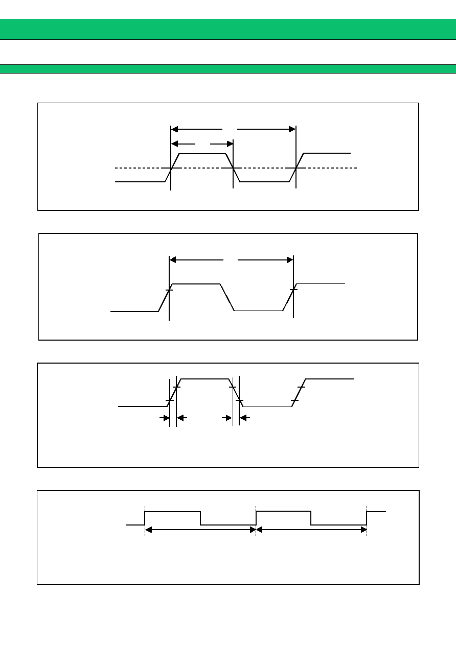
OUTPUT CLOCK Duty Cycle (t
DCC
, t
DCR
=
t
b
/t
a
)
INPUT FREQUENCY (f
in
=
1/t
in
)
OUTPUT SLEW RATE (SR
C
, SR
R
)
CYCLE-CYCLE JITTER (t
JC
= |t
n
-t
n+1
|)
CKOUT
REFOUT
1.5 V
t
a
t
b
0.8 V
DD
t
in
XIN
2.4 V
0.4 V
t
f
t
r
CKOUT
REFOUT
Note : SR
C
=
(2.4
-
0.4) /t
r
, SR
C
=
(2.4
-
0.4) /t
f
SR
R
=
(2.4
-
0.4) /t
r
, SR
R
=
(2.4
-
0.4) /t
f
t
n+1
t
n
CKOUT
Note : Cycle-cycle jitter indicates the difference between a certain cycle and the immediately
succeeding (or preceding) cycle.
MB88156
17
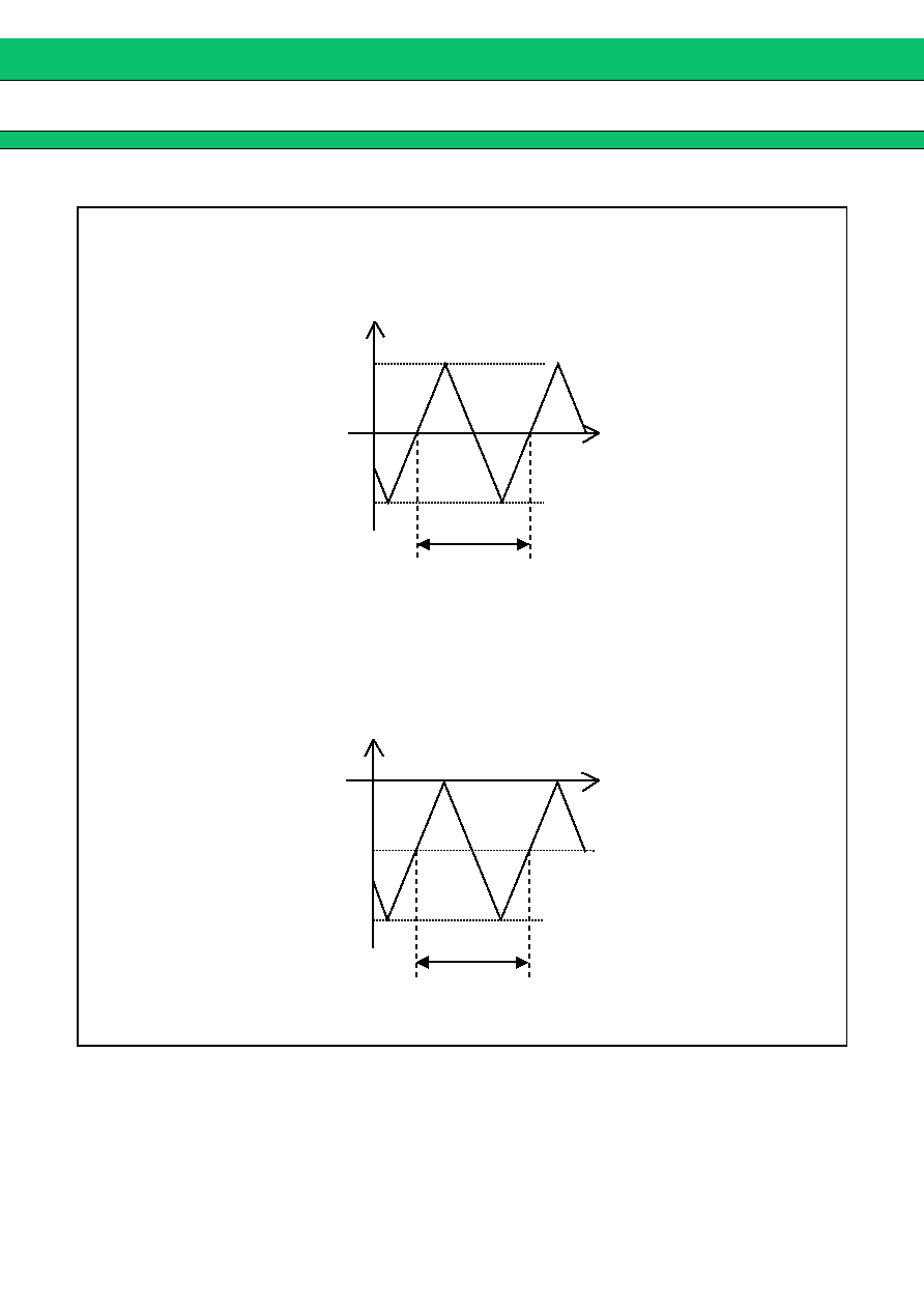
MODULATION WAVEFORM
f
MOD
(Typ)
=
32.4 kHz (fin
=
24 MHz)
-
1.0 %
+
1.0 %
-
1.0 %
-
0.5 %
f
MOD
(Typ)
=
32.4 kHz (fin
=
24 MHz)
∑
Modulation rate
±
1.0
%
, example of center spread
∑
Modulation rate
-
1.0
%
, example of down spread
CKOUT
output frequency
CKOUT
output frequency
Frequency at
modulation off
Frequency at
modulation off
Time
Time
MB88156
18
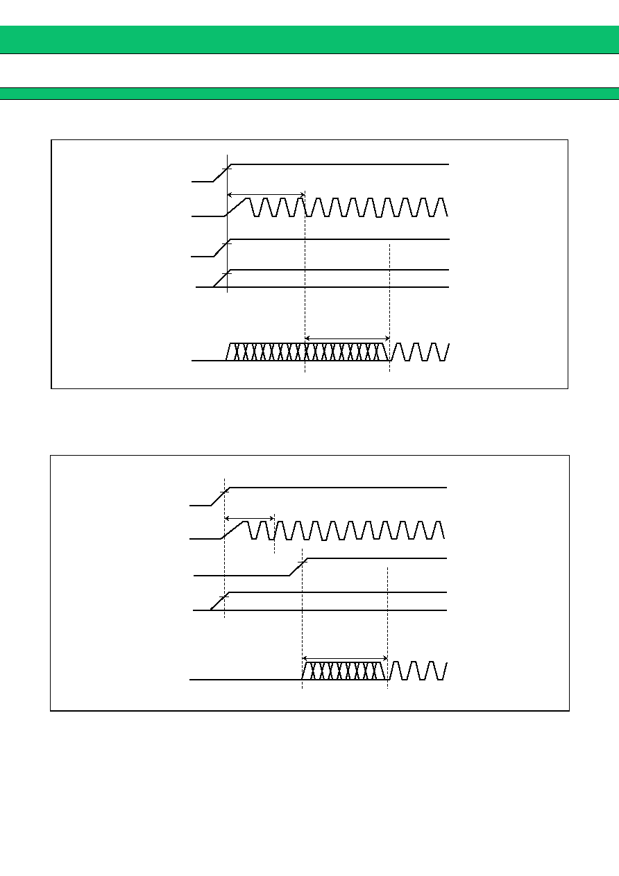
LOCK-UP TIME
If the XPD pin is fixed at the "H" level, the maximum time after the power is turned on until the set clock signal is
output from CKOUT pin is (the stabilization wait time of input clock to XIN pin)
+
(the lock-up time "t
LK
"). For the
input clock stabilization time, check the characteristics of the resonator or oscillator used.
If the XPD pin is used for power-down control, the set clock signal is output from the CKOUT pin at most the lock-
up time "t
LK
" after the XPD pin goes "H" level.
(Continued)
3.0 V
V
DD
XIN
XPD
V
IH
V
IH
CKOUT
External clock
stabilization wait time
t
LK
(Lock-up time)
SPRD,
MLTP0,
MLTP1,
FREQ, ENS,
SEL
V
IH
V
IH
3.0 V
V
DD
XIN
XPD
CKOUT
External clock
stabilization wait time
t
LK
(Lock-up time)
SPRD,
MLTP0,
MLTP1,
FREQ,
ENS,
SEL
MB88156
19
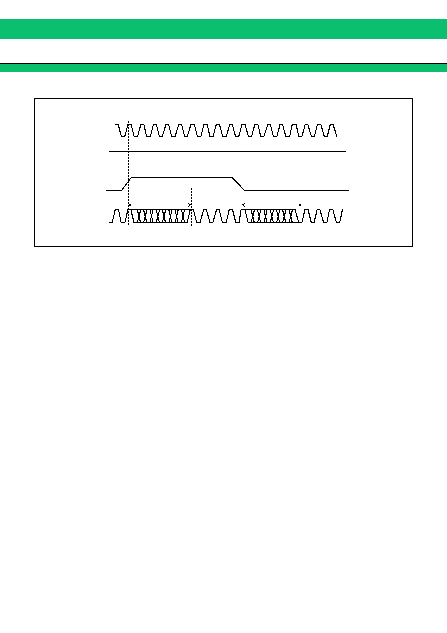
(Continued)
If the ENS pin is used for modulation enable control during normal operation, the set clock signal is output from the
CKOUT pin at most the lock-up time "t
LK
" after the level at the ENS pin is determined.
Note : The wait time for the clock signal output from the CKOUT pin to become stable is required after the IC is
released from power-down mode by the XPD pin or after another pin's setting is changed. During the period
until the output clock signal becomes stable, neither of the output frequency, output clock duty cycle, mod-
ulation period, and cycle-cycle jitter characteristic cannot be guaranteed. It is therefore advisable to take
action, such as cancelling a device reset at the stage after the lock-up time has passed.
V
IL
V
IH
V
IH
XIN
XPD
ENS
CKOUT
t
LK
(Lock-Up time)
t
LK
(Lock-Up time)
MB88156
20
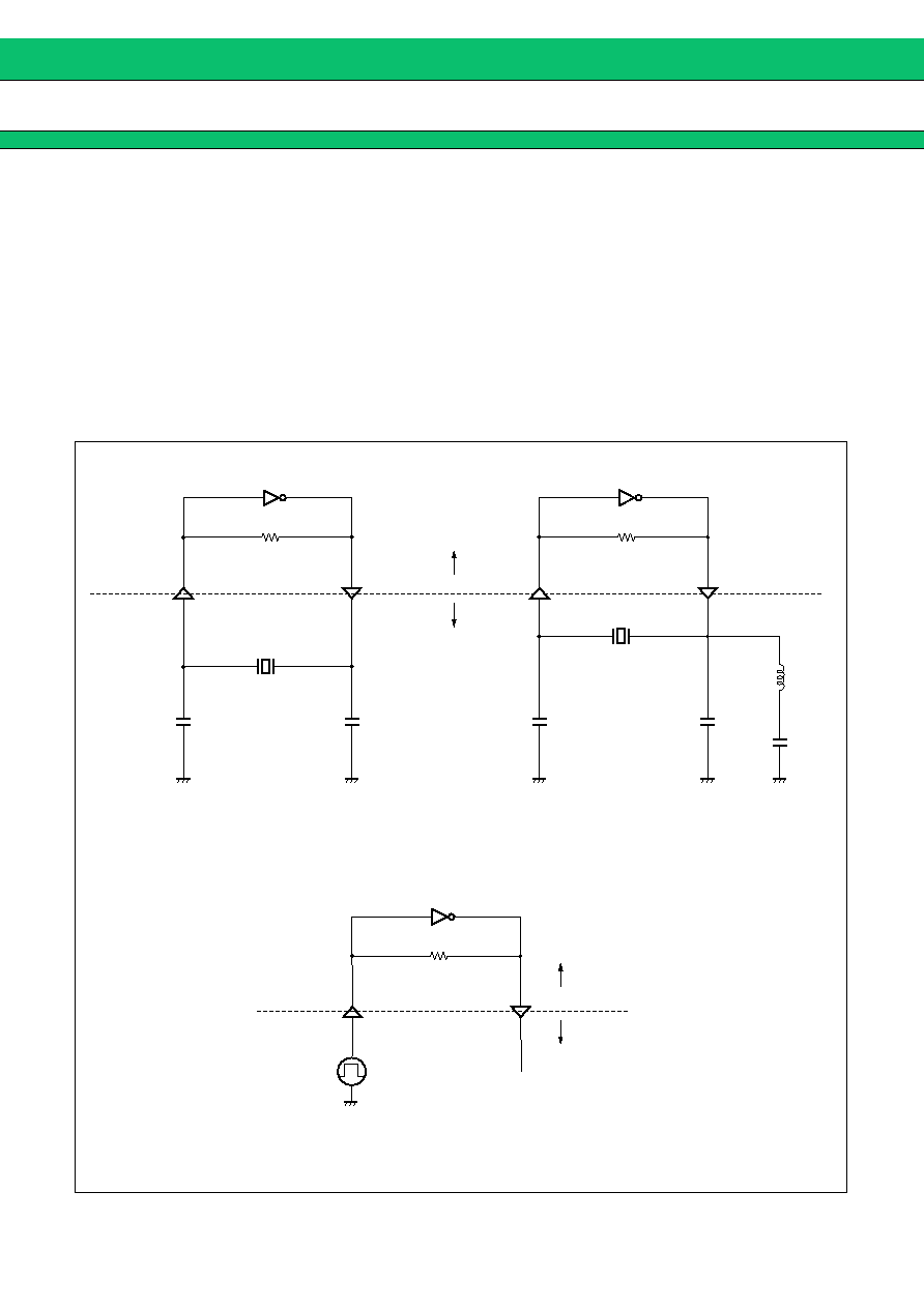
OSCILLATION CIRCUIT
The following schematic on the left-hand side shows a sample connection of a general resonator. The oscillation
circuit contains a feedback resistor (1 M
) . The values of capacitors (C
1
and C
2
) must be adjusted to the optimum
constant of the resonator used.
The following schematic on the right-hand side shows a sample connection of a 3rd overtone resonator. The
values of capacitors (C
1
, C
2
, and C
3
) and inductor (L
1
) must be adjusted to the optimum constant of the resonator
used.
The most suitable value is different by individual resonator. Please refer to the resonator manufacturer which
you use for the most suitable value.
To use an external clock signal (without using the resonator) , input the clock signal to the XIN pin with the XOUT
pin connected to nothing .
C
1
R
f
(1 M
)
C
2
C
1
L
1
R
f
(1 M
)
C
2
C
3
XIN pin
XOUT pin
XIN pin
XOUT pin
LSI internal
LSI external
Fundamental resonator
3rd overtone resonator
∑
When using the resonator
OPEN
R
f
(1 M
)
∑
When using the external clock
Note : Note that the jitter characteristic of the input clock signal may affect the cycle-cycle jitter
characteristic.
LSI internal
LSI external
XOUT pin
External clock
XIN pin
MB88156
21
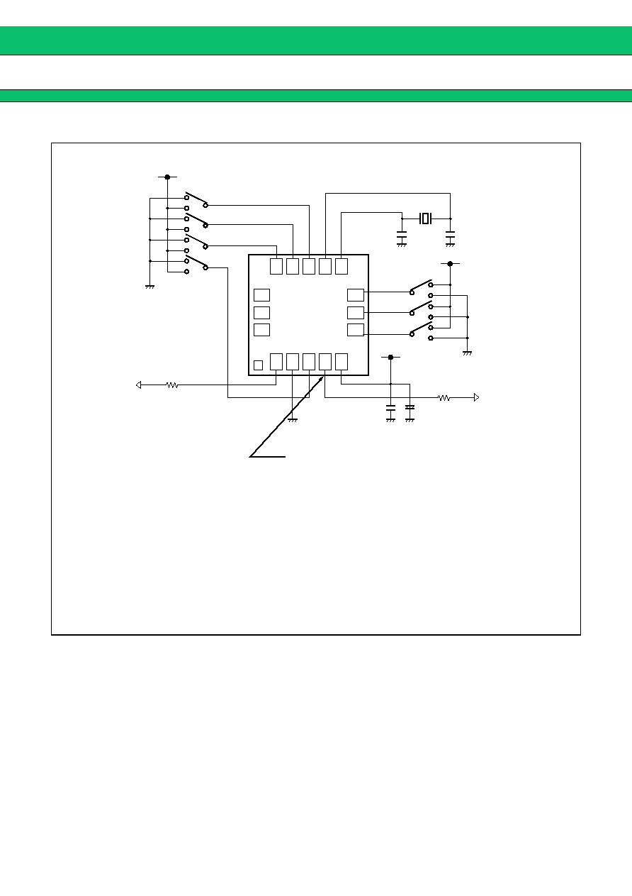
INTERCONNECTION CIRCUIT EXAMPLE
MLTP0
FREQ
MLTP1
14
15
16
8
7
6
13
1
2
3
4
5
12 11 10
9
MB88156
XOUT
ENS
XPD
SEL
XIN
CKOUT
SPRD
R
1
V
SS
V
DD
REFOUT
C
4
C
1
C
2
C
3
R
2
C
1
, C
2
: Oscillation stabilization capacitance (see
OSCILLATION CIRCUIT)
C
3
: Capacitor of 10
µ
F or higher
C
4
: Capacitor of about 0.01
µ
F (connect a capacitor of good high frequency
property (ex. laminated ceramic capacitor) to close to this device)
R
1
, R
2
: Impedance matching resistor for board pattern
For the MB88156-001, be sure to open because
it becomes N.C. pin.
MB88156
22
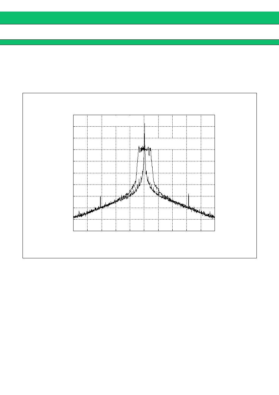
SPECTRUM EXAMPLE CHARACTERISTICS
The condition of the examples of the characteristic is shown as follows : Input frequency
=
16 MHz (Output
frequency
=
64 MHz : Using MB88156-001 (Multiplied by 4) )
Power-supply voltage
=
3.3 V, None load capacity. Modulation rate
=
±
1.0
%
(center spread).
Spectrum analyzer HP4396B is connected with CKOUT. The result of the measurement with RBW
=
1 kHz (
ATT
use for
-
6 dB
) .
CH B Spectrum
10 dB /REF 0 dBm
Avg
4
RBW# 1 kH
Z
VBW 1 kH
Z
ATT 6 dB
CENTER 64 MH
Z
SWP 8.005 s
SPAN 12.8 MH
Z
No modulation
-
7.33 dBm
±
1.0
%
modulation
-
26.26 dBm

MB88156
23
ORDERING INFORMATION
Part number
REFOUT pin
Package
Emboss taping
MB88156PV-G-000-EFE1
Provided
16-pin plastic BCC
(LCC-16P-M09)
EF type
MB88156PV-G-000-ERE1
ER type
MB88156PV-G-001-EFE1
None
EF type
MB88156PV-G-001-ERE1
ER type
MB88156
24
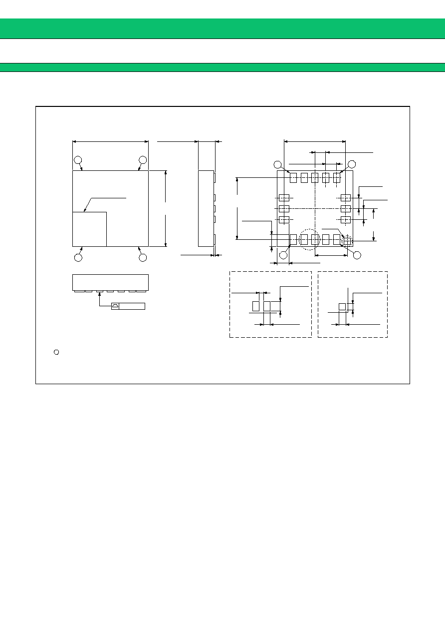
PACKAGE DIMENSION
16-pin plastic BCC
(LCC-16P-M09)
Dimensions in mm (inches)
Note : The values in parentheses are reference values.
C
2004 FUJITSU LIMITED C16067S-c-1-1
0.50±0.10
(.020±.004)
"A"
0.55±0.07
(.022±.003)
3.50±0.10
(.138±.004)
0.80(.031)MAX
Mount height
0.075±0.025
(.003±.001)
(Stand off)
0.05(.002)
5
1
13
9
13
1
5
1.50(.059)
REF
1.50(.059)
REF
"B"
Details of "B" part
(.012±.002)
0.30±0.06
(.012±.002)
0.30±0.06
INDEX AREA
(.138±.004)
3.50±0.10
2.85(0.112)
TYP
(.012±.002)
0.30±0.06
(.018±.002)
0.45±0.06
Details of "A" part
2.85(.112)TYP
0.50(.020)
TYP
9
0.55±0.07
(.022±.003)
0.50(.020)
TYP
0.50±0.10
(.020±.004)
INDEX
0.14(.006)
MIN

MB88156
FUJITSU LIMITED
All Rights Reserved.
The contents of this document are subject to change without notice.
Customers are advised to consult with FUJITSU sales
representatives before ordering.
The information, such as descriptions of function and application
circuit examples, in this document are presented solely for the
purpose of reference to show examples of operations and uses of
Fujitsu semiconductor device; Fujitsu does not warrant proper
operation of the device with respect to use based on such
information. When you develop equipment incorporating the
device based on such information, you must assume any
responsibility arising out of such use of the information. Fujitsu
assumes no liability for any damages whatsoever arising out of
the use of the information.
Any information in this document, including descriptions of
function and schematic diagrams, shall not be construed as license
of the use or exercise of any intellectual property right, such as
patent right or copyright, or any other right of Fujitsu or any third
party or does Fujitsu warrant non-infringement of any third-party's
intellectual property right or other right by using such information.
Fujitsu assumes no liability for any infringement of the intellectual
property rights or other rights of third parties which would result
from the use of information contained herein.
The products described in this document are designed, developed
and manufactured as contemplated for general use, including
without limitation, ordinary industrial use, general office use,
personal use, and household use, but are not designed, developed
and manufactured as contemplated (1) for use accompanying fatal
risks or dangers that, unless extremely high safety is secured, could
have a serious effect to the public, and could lead directly to death,
personal injury, severe physical damage or other loss (i.e., nuclear
reaction control in nuclear facility, aircraft flight control, air traffic
control, mass transport control, medical life support system, missile
launch control in weapon system), or (2) for use requiring
extremely high reliability (i.e., submersible repeater and artificial
satellite).
Please note that Fujitsu will not be liable against you and/or any
third party for any claims or damages arising in connection with
above-mentioned uses of the products.
Any semiconductor devices have an inherent chance of failure. You
must protect against injury, damage or loss from such failures by
incorporating safety design measures into your facility and
equipment such as redundancy, fire protection, and prevention of
over-current levels and other abnormal operating conditions.
If any products described in this document represent goods or
technologies subject to certain restrictions on export under the
Foreign Exchange and Foreign Trade Law of Japan, the prior
authorization by Japanese government will be required for export
of those products from Japan.
F0503
©
2005 FUJITSU LIMITED Printed in Japan