/home/web/doc/html/fujitsu/180454
1
DS04-13506-1E
FUJITSU SEMICONDUCTOR
DATA SHEET
LINEAR IC
R-2R TYPE 8-BIT D/A CONVERTER WITH
OPERATIONAL AMPLIFIER OUTPUT BUFFERS
MB88347
s
DESCRIPTION
The Fujitsu MB88347 is an R-2R type 8-bit resolution digital-to-analog converter (DAC), designed for interface with
a wide range of general 4-bit and 8-bit microcontrollers including Fujitsu's MB88200 family, MB8850 family, and
MB88500 family 4-bit single-chip microcontrollers.
The MB88347 has an 8-bit
×
8-channel D/A converter with operational amplifier output buffers. Digital data are input
serially by individual channel units. The loaded digital data are converted into analog DC voltages by the D/A converter
in 100
µ
s settling time. Also, the MB88347 has operational amplifier output buffers. These operational amplifier
output buffers are connected to each channel of the D/A converter, and provide high current drive capability. The
MB88347 is suitable for electronic volumes and replacement for potentiometers for adjustment, in addition to normal
D/A converter applications.
s
FEATURES
· Conversion method : R-2R resistor ladder
· 8-bit
×
8-channel D/A converter with operational amplifier output buffers
· Max. 2.5 MHz Serial data input
· Serial data output for cascade connection
· Max. 100
µ
s DAC output settling time
· Max. +1.0/1.0 mA analog output sink/source current
· Two separate power supply/ground lines for MCU interface block/operational amplifier output buffer block and
D/A converter block
(Continued)
s
PACKAGE
This device contains cirduitry to protect the inputs against damage due to high static voltages or electric fields. However, it is advised that normal precautions be
taken to avoid application of any voltage higher than maximum rated voltages to this high impedance circuit.
PLASTIC DIP
(DIP-16P-M04)
PLASTIC SOP
(FPT-16P-M06)
PLASTIC SSOP
(FPT-16P-M05)
MB88347-P
MB88347-PF
MB88347-PFV
2
MB88347
(Continued)
· Pin compatible with MB88342
· Single +5 V power supply
· Wide operating temperature range: 20
°
C to +85
°
C
· Silicon-gate CMOS process
· Three package options :
16-pin plastic DIP (Suffix : -P), 16-pin plastic SOP (Suffix : -PF), 16-pin plastic SSOP(Suffix : -PFV)
s
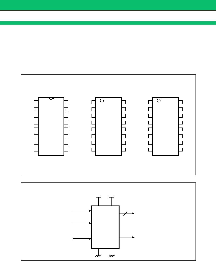
PIN ASSIGNMENT
AO3
AO4
AO2
V
SS
AO5
AO6
AO7
V
DD
1
2
3
4
5
6
7
8
16
15
14
13
12
11
10
9
GND
AO1
DI
CLK
LD
DO
AO8
V
CC
MB88347-P
MB88347-PF
(Top View)
MB88347-PFV
V
SS
AO2
AO3
AO4
AO5
AO6
AO7
V
DD
1
2
3
4
5
6
7
8
16
15
14
13
12
11
10
9
GND
DI
CLK
LD
DO
V
CC
(Top View)
AO1
AO8
V
SS
AO2
AO3
AO4
AO5
AO6
AO7
V
DD
1
2
3
4
5
6
7
8
16
15
14
13
12
11
10
9
GND
DI
CLK
LD
DO
V
CC
(Top View)
AO1
AO8
Figure 1 Logic Symbol
+5 V
+5 V
AO1 AO8
DO
DI
LD
CLK
V
DD
V
CC
GND
V
SS
MB88347
DAC Output
Data Input
Load Strobe Input
Shift Clock Input
8
Data Output
3
MB88347
s
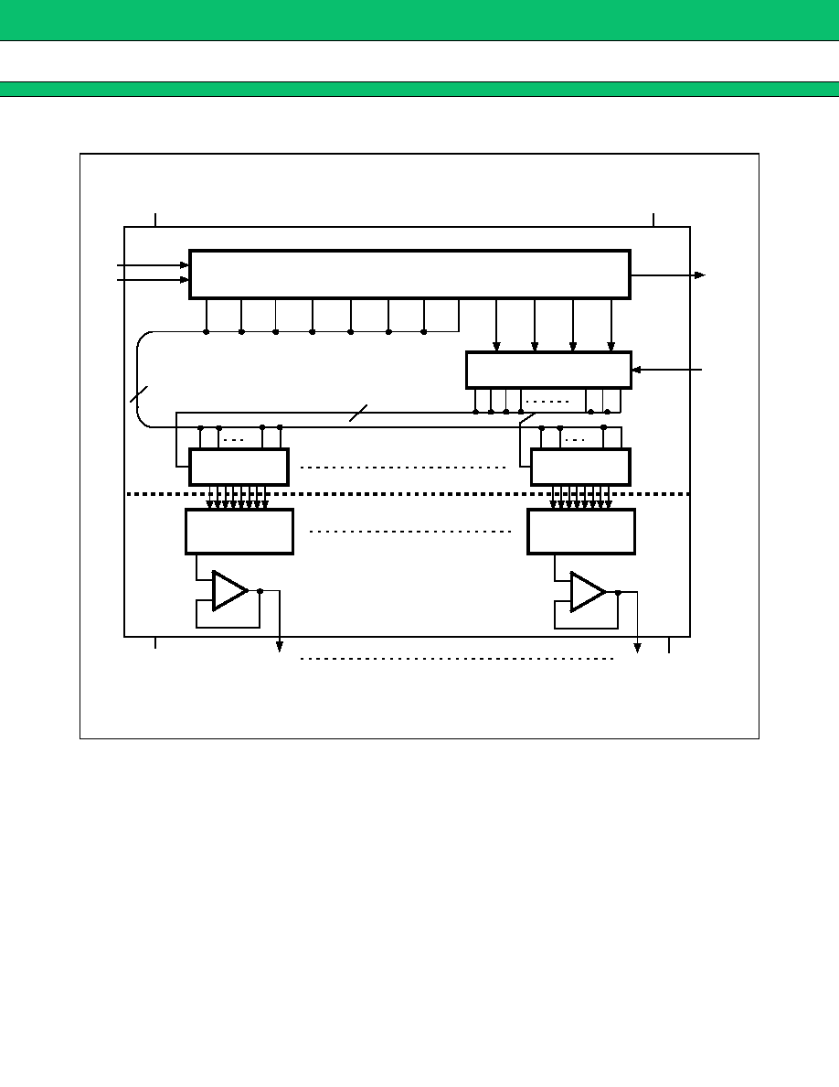
BLOCK DIAGRAM
D7
D7
D6
D1
D0
LD
DO
12-bit Shift Register
V
CC
GND
DI
CLK
D0
D1
D2
D3
D4
D5
D6
D7
D8
D9
D10
D11
8
8
8-bit Data Latch
#1
1 2 3 4
8
4-bit Address Decoder
V
SS
*
V
DD
*
AO8
AO1
R-2R Type 8-bit
D/A Converter
#1
Analog Block (D/A Converter with operational
amplifier output buffers)
Digital Block (MCU Interface)
6 7
D6
D1
D0
8-bit Data Latch
#8
R-2R Type 8-bit
D/A Converter
#8
+
+
* : Only for D/A converter block except operational amplifier block
4
MB88347
s
PIN DESCRIPTION
PIN ASSIGNMENT and Table 1 show the pin assignment and pin description of the MB88347.
Table 1 Pin Description
Symbol
Pin No.
Type
Name & Function
Power Supply
V
CC
9
--
+5 V DC power supply pin for the digital block (MCU interface) and oper-
ational amplifier output buffers.
GND
16
--
Ground pin for the digital block (MCU interface) and operational ampli-
fier output buffers.
V
DD
8
--
DC power supply pin for the analog block (D/A converter) except opera-
tional amplifier output buffers.
V
SS
1
--
Ground pin for the analog block (D/A converter) except operational
amplifier output buffers.
Control Input
CLK
13
I
Shift clock input to the internal 12-bit shift register: At the rising edge of
CLK data on the DI pin is shifted into the LSB of the shift register and
contents of the shift register are shifted right (to the MSB).
LD
12
I
Load strobe input for a 12-bit address/data : A high level on the LD pin
latches a 4-bit address (upper 4 bits: D11 to D8) of the internal 12-bit
shift register into the internal address decoder, and writes 8-bit data
(lower 8 bits: D7 to D0) of the shift register into an internal data latch
selected by the latched address.
Data Input/Output
DI
14
I
Serial address/data input to the internal 12-bit shift register: The
address/data format is that upper 4 bits (D11 to D8) indicate an address
and lower 8 bits (D7 to D0) indicate data. The D11 (MSB) is the first-in
bit and D0 (LSB) is the last-in bit.
DO
11
O
Serial address/data output from the internal 12-bit shift register: This is
an output pin of the MSB bit data of the 12-bit shift register. This pin
allows a cascade connection of the device.
DAC Output
AO1
AO2
AO3
AO4
AO5
AO6
AO7
AO8
15
2
3
4
5
6
7
10
O
8-bit resolution D/A converter outputs : 8 channels (AO1 to AO8)
Each output channel has an operational amplifier output buffer for ana-
log output data.
5
MB88347
s
FUNCTIONAL DESCRIPTION
OVERVIEW
The MB88347 is a R-2R resistor ladder type, 8-bit resolution digital-to-analog converter (DAC) device. The MB88347
has 8 channels of D/A converters with operational amplifier output buffers. 8-bit digital data are loaded into internal
data latches by individual DAC channel units. The loaded digital data are converted into analog DC voltages through
the internal D/A converter in max. 100
µ
s settling time. And the analog DC voltages source/sink the output current
through the operational amplifier output buffers. For cascade connection, a serial data output is provided.
DEVICE CONFIGURATION
As illustrated in BLOCK DIAGRAM, the MB88347 device is composed by the digital block (MCU interface) and
analog block (D/A converter with operational amplifier output buffers). The digital block consists of a 12-bit shift
register, a 4-bit address decoder, and 8-channels of 8-bit data latches. The analog block includes 8-channels of 8-
bit D/A converters with operational amplifier output buffers connecting to the data latches. For electrically stable
operation the power supply and ground lines are separate between the digital block (MCU interface) and operational
amplifier output buffers, and analog block except operational amplifier output buffers.
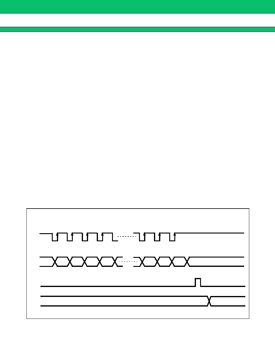
DEVICE OPERATION
Figure 2 shows the input/output timing. A 12-bit address/data is serially input into the shift register through the DI
pin synchronously with the rising edge of CLK. The format of the shift register is shown in Figure 3. The lower 8
bits (D7 to D0) are data bits to be converted, and the upper 4 bits are address bits (D11 to D8) to select a data latch
to be written. A high level on the LD pin loads the address decoder with the 4-bit address to select a data latch,
and writes the 8-bit data into a selected data latch. Figure 4 shows the data latch address map, and Table 2, address
decoding. 8-bit data written into individual data latches are converted into analog DC voltages, dividing the supply
voltage |V
DD
-V
SS
| through R-2R resistor ladders of D/A converters. The operational amplifier output buffers at
individual D/A converter outputs can source up to 1.0 mA of the output current. Figure 5 shows a configuration of
the R-2R resistor ladder D/A converter with operational amplifier, and Table 3 analog DC voltages corresponding
to each digital data.
Figure 2 Input/Output Timing
DI
CLK
LD
AOx
MSB
LSB
D11
D10
D9
D8
D2
D1
D0
Previous Data
New Data
Document Outline