DS07-12561-1E
FUJITSU SEMICONDUCTOR
DATA SHEET
8-bit Proprietary Microcontroller
CMOS
F
2
MC-8L MB89202 Series
MB89202/F202/V201
DESCRIPTION
The MB89202 series is a line of single-chip microcontrollers. In addition to a compact instruction set, the micro-
controllers contain a variety of peripheral functions such, timers, a serial interface, an A/D converter and an
external interrupt.
FEATURES
∑ F
2
MC-8L family CPU core
∑ Maximum memory space : 64 Kbytes
∑ Minimum execution time : 0.32
µ
s/12.5 MHz
∑ Interrupt processing time : 2.88
µ
s/12.5 MHz
∑ I/O ports : Max 26 channels
∑ 21-bit time-base timer
∑ 8-bit PWM timer
∑ 8/16-bit capture timer/counter
∑ 10-bit A/D converter : 8 channels
∑ UART
∑ 8-bit serial I/O
∑ External interrupt 1 : 3 channels
∑ External interrupt 2 : 8 channels
∑ Wild Register : 2 bytes
(Continued)
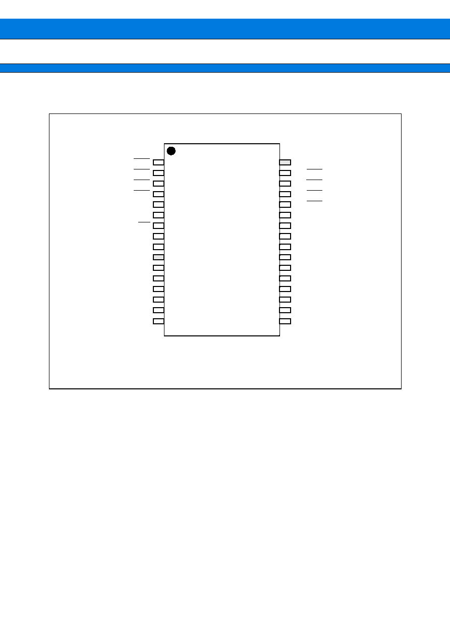
PACKAGES
32-pin plastic SH-DIP
34-pin plastic SSOP
(DIP-32P-M06)
(FPT-34P-M03)
MB89202 Series
2
(Continued)
∑ MB89F202 : Flash (at least 10,000 program / erase cycles) with read protection
∑ Low-power consumption modes ( sleep mode, and stop mode)
∑ SH-DIP-32, SSOP-34 package
∑ CMOS Technology
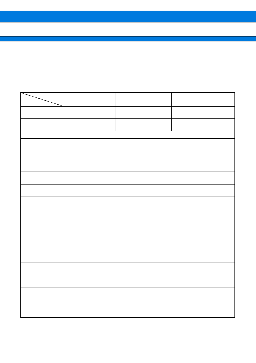
PRODUCT LINEUP
(Continued)
Part number
MB89202
MB89F202
MB89V201
Parameter
Classification
Mask ROM product
Flash memory product
(read protection)
Evaluation product
(for development)
ROM size
16 K
◊
8 bits
(internal mask ROM)
16 K
◊
8 bits
(internal flash)
32K x 8 bits
(external EPROM)
RAM size
512
◊
8 bits
CPU functions
Number of instructions :
Instruction bit length :
Instruction length :
Data bit length :
Minimum execution time :
Interrupt processing time :
136
8 bits
1 to 3 bytes
1, 8, 16 bits
0.32
µ
s to 5.1
µ
s (12.5 MHz)
2.88
µ
s to 46.1
µ
s (12.5 MHz)
Ports
General-purpose I/O ports (CMOS) : 26 (also serve as peripherals )
(4 ports are also an N-ch open-drain type.)
21-bit time-base
timer
21-bit Interrupt cycle : 0.66 ms, 2.64 ms, 21 ms, or 335.5 ms with 12.5 MHz main clock
Watchdog timer
Reset generation cycle : 335.5 ms minimum with 12.5 MHz main clock
8-bit PWM timer
8-bit interval timer operation (square output capable, operating clock cycle :
0.32
µ
s , 2.56
µ
s, 5.1
µ
s, 20.5
µ
s)
8-bit resolution PWM operation (conversion cycle : 81.9
µ
s to 21.47 s : in the selection of
internal shift clock of 8/16-bit capture timer)
Count clock selectable between 8-bit and 16-bit timer/counter outputs
8/16-bit capture,
timer/counter
8-bit capture timer/counter
◊
1 channel
+
8-bit timer or
16-bit capture timer/counter
◊
1 channel
Capable of event count operation and square wave output using external clock input with
8-bit timer 0 or 16-bit counter
UART
Transfer data length : 6/7/8 bits
8-bit Serial I/O
8 bits LSB first/MSB first selectable
One clock selectable from four operation clocks
(one external shift clock, three internal shift clocks : 0.8
µ
s, 6.4
µ
s, 25.6
µ
s)
12-bit PPG timer
Output frequency : Pulse width and cycle selectable
External interrupt 1
(wake-up function)
3 channels (Interrupt vector, request flag, request output enabled)
Edge selectable (Rising edge, falling edge, or both edges)
Also available for resetting stop/sleep mode (Edge detectable even in stop mode)
External interrupt 2
(wake-up function)
1 channel with 8 inputs (Independent L-level interrupt and input enable)
Also available for resetting stop/sleep mode (Level detectable even in stop mode)
MB89202 Series
3
(Continued)
*1 : Check section "
MASK OPTIONS"
*2 : The minimum operating voltage varies with the operating frequency, the function, and the connected ICE. (The
operating voltage of the A/D converter is assured separately. Check section "
ELECTRICAL CHARACTER-
ISTICS.")
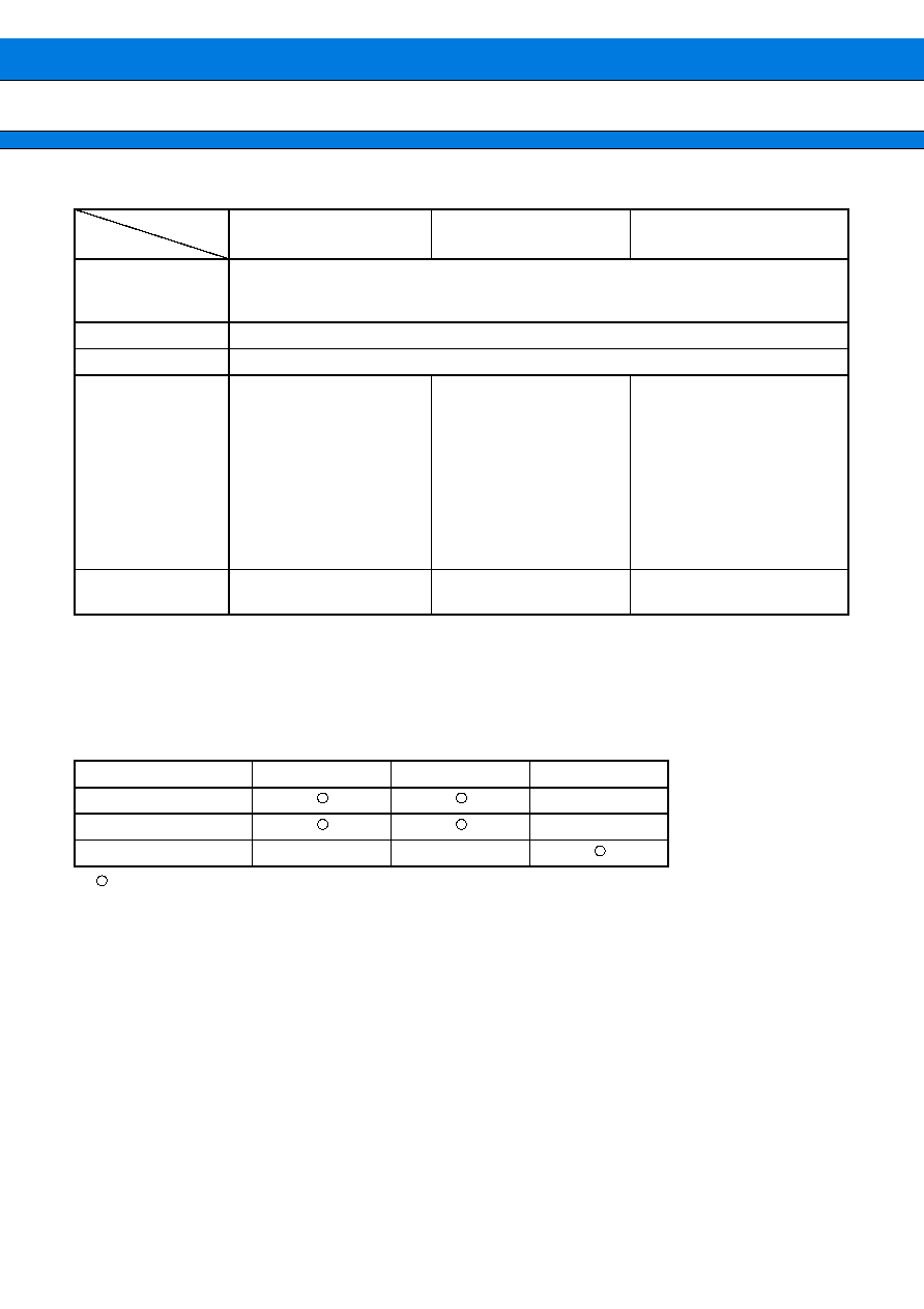
PACKAGE AND CORRESPONDING PRODUCTS
: Available
◊
: Not available
DIFFERENCES AMONG PRODUCTS
∑ Memory Size
Before evaluating using the evaluation product, verify its differences from the product that will actually be used.
∑ Mask Options
Functions that can be selected as options and how to designate these options vary by the product. Before using
options check section "
MASK OPTIONS".
Part number
MB89202
MB89F202
MB89V201
Parameter
10-bit A/D converter
10-bit precision
◊
8 channels
A/D conversion function (Conversion time : 12.16
µ
s/12.5 MHz)
Continuous activation by 8/16-bit timer/counter output or time-base timer counter
Wild Register
8-bit
◊
2
Standby mode
Sleep mode, and Stop mode
Overhead time from
reset to the first
instruction execution
Power-on reset :
Oscillation stabillization
wait*
1
External reset : a few
µ
s
Software reset : a few
µ
s
Power-on reset :
Voltage regulator and
oscillation stabillization
wait
(31.5 ms/12.5 MHz)
External reset :
Oscillation stabillization
wait
(21.0 ms/12.5 MHz)
Software reset : a few
µ
s
Power-on reset :
Oscillation stabillization
wait
(21.0 ms / 12.5 MHz)
External reset :
Oscillation stabillization
wait
(21.0 ms / 12.5 MHz)
Software reset : a few
µ
s
Power supply
voltage*
2
2.2 V to 5.5 V
3.5 V to 5.5 V
2.7 V to 5.5 V
Package MB89202
MB89F202
MB89V201
DIP-32P-M06
◊
FPT-34P-M03
◊
FPT-64P-M03
◊
◊