DS07-12552-1E
FUJITSU SEMICONDUCTOR
DATA SHEET
8-bit Proprietary Microcontroller
CMOS
F
2
MC-8L MB89470 Series
MB89475/P475/PV470
s
DESCRIPTION
The MB89470 series has been developed as a general-purpose version of the F
2
MC*-8L family consisting of
proprietary 8-bit, single-chip microcontrollers.
In addition to a compact instruction set, the microcontroller contains a variety of peripheral functions such as 21-
bit time-base timer, watch prescaler, PWC timer, PWM timer, 8/16-bit timer/counter, external interrupt 1 (edge) ,
external interrupt 2 (level) , 10-bit A/D converter, UART/SIO, buzzer, watchdog timer reset.
The MB89470 series is designed suitable for home appliance as well as in a wide range of applications for
consumer product.
* : F
2
MC stands for FUJITSU Flexible Microcontroller.
s
FEATURES
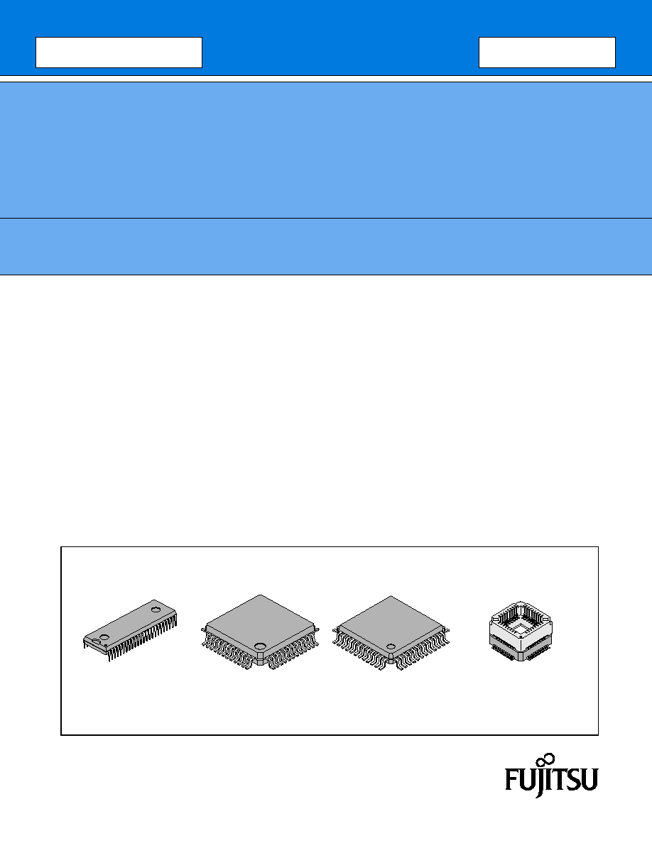
∑ Package used
QFP package, LQFP package and SH-DIP package for MB89P475, MB89475
MQFP package for MB89PV470
(Continued)
s
PACKAGES
48-pin Plastic SH-DIP
48-pin Plastic LQFP
48-pin Plastic QFP
48-pin Ceramic MQFP
(DIP-48P-M01)
(FPT-48P-M05)
(FPT-48P-M13)
(MQP-48C-P01)

MB89470 Series
2
(Continued)
∑ High-speed operating capability at low voltage
∑ Minimum execution time : 0.32
µ
s/12.5 MHz
∑ F
2
MC-8L family CPU core
∑ Six timers
PWC timer (also usable as an interval timer)
PWM timer
8/16-bit timer/counter
◊
2
21-bit timebase timer
Watch prescaler
∑ Buzzer
7 frequency types are selectable by software
∑ External interrupts
Edge detection (Selectable edge) : 4 channels
Low-level interrupt (Wake-up function) : 5 channels
∑ A/D converter (8 channels)
10-bit successive approximation type
∑ UART/SIO
Synchronous/asynchronous data transfer capable
∑ Low-power consumption modes
Stop mode (Oscillation stops to minimize the current consumption.)
Sleep mode (The CPU stops to reduce the current consumption to approx. 1/3 of normal.)
Subclock mode (for dual clock product)
Watch mode (for dual clock product)
∑ Watch dog timer reset
∑ I/O ports : Max 39 channels
Multiplication and division instructions
Instruction set optimized for controllers
16-bit arithmetic operations
Bit test and branch instructions
Bit manipulation instructions, etc.
MB89470 Series
3
s
PRODUCT LINEUP
(Continued)
Part number
Parameter
MB89475
MB89P475
MB89PV470
Classification
Mass production products
(mask ROM product)
OTP
Piggy-back
ROM size
16 K
◊
8-bit (internal ROM)
16 K
◊
8-bit (internal PROM,
can be written to by FLASH
programmer)
32 K
◊
8-bit (external ROM)
RAM size
512
◊
8 bits
1 K
◊
8 bits
CPU functions
Number of instructions
Instruction bit length
Instruction length
Data bit length
Minimum execution time
Minimum interrupt processing time
: 136
: 8 bits
: 1 to 3 bytes
: 1, 8, 16 bits
: 0.32
µ
s/12.5 MHz
: 2.88
µ
s/12.5 MHz
Ports
Output-only ports (N-channel open drain)
Input-only ports
I/O ports (CMOS)
Total
: 7 pins
: 3 pins (1 pin in product with
dual clock)
: 29 pins
: 39 pins
21-bit Time-base
timer
Interrupt period (0.82 ms, 3.3 ms, 26.2 ms, 419.4 ms) at 10 MHz
Interrupt period (0.66 ms, 2.6 ms, 21.0 ms, 335.5 ms) at 12.5 MHz
Watchdog timer
Reset period (209.7 ms to 419.4 ms) at 10 MHz
Reset period (167.8 ms to 335.5 ms) at 12.5 MHz
Watch prescaler
17 bits
Interrupt cycle : 31.25 ms, 0.25 ms, 0.5 s, 1.00 s, 2.00 s, 4.00 s/32.768 kHz for subclock
Pulse width count
timer
2 channels
8-bit one-shot timer operation (supports underflow output, operating clock period : 1, 4, 32
t
inst
*, external)
8-bit reload timer operation (supports square wave output, operating clock period : 1, 4,
32 t
inst
*, external)
8-bit pulse width measurement operation (supports continuous measurement, H width, L
width, rising edge to rising edge, falling edge to falling edge measurement and both edge
measurement)
PWM timer
8-bit reload timer operation (supports square wave output, operating clock period : 1, 4,
32 t
inst
*, external)
8-bit resolution PWM operation
8/16-bit timer/
counter 1, 2
Can be operated either as a 2-channel 8-bit timer/counter (Timer 1 and Timer 2, each with
its own independent operating clock cycle) , or as one 16-bit timer/counter
In Timer 1 or 16-bit timer/counter operation, event counter operation (external clock-trig-
gered) and square wave output capable
8/16-bit timer/
counter 3, 4
Can be operated either as a 2-channel 8-bit timer/counter (Timer 3 and Timer 4, each with
its own independent operating clock cycle) , or as one 16-bit timer/counter
In Timer 3 or 16-bit timer/counter operation, event counter operation (external clock-trig-
gered) and square wave output capable
External interrupt
4 independent channels (selectable edge, interrupt vector, request flag)
5 channels (low level interrupt)
MB89470 Series
4
(Continued)
* : t
inst
is one instruction cycle (execution time) , which can be selected as 1/4, 1/8, 1/16, or 1/64 of main clock.
s
PACKAGE AND CORRESPONDING PRODUCTS
O : Available
X : Not available
s
DIFFERENCES AMONG PRODUCTS
1.
Memory Size
Before evaluating using the piggyback product, verify its differences from the product that will actually be used.
Take particular care on the following point :
∑ The stack area, etc., is set at the upper limit of the RAM.
2.
Current Consumption
∑ For the MB89PV470, add the current consumed by the EPROM mounted in the piggy-back socket.
∑ When operating at low speed, the current consumed by the one-time PROM product is greater than that for
the mask ROM product. However, the current consumption are roughly the same in sleep or stop mode.
∑ For more information, see "
s
ELECTRICAL CHARACTERISTICS".
3.
Oscillation stabilization time after power-on reset
∑ For MB89PV470, there is no power-on stabilization time after power-on reset.
∑ For MB89P475, there is power-on stabilization time after power-on reset.
∑ For MB89475, the power-on stabilization time can be select.
∑ For more information, refer to "
s
MASK OPTIONS".
Part number
Parameter
MB89475
MB89P475
MB89PV470
A/D converter
10-bit resolution
◊
8 channels
A/D conversion function (conversion time : 60 t
inst
*)
Supports repeated activation by internal clock.
UART/SIO
Synchronous/asynchronous data transfer capable
(Max baud rate : 78.125 Kbps at 10 MHz)
(7 and 8 bits with parity bit ; 8 and 9 bits without parity bit)
Buzzer output
7 frequency types (F
CH
/2
12
, F
CH
/2
11
, F
CH
/2
10
, F
CH
/2
9
, F
CL
/2
5
, F
CL
/2
4
, F
CL
/2
3
) are selectable by
software.
Standby mode
Sleep mode, stop mode, subclock mode (dual clock product) and watch mode (dual clock
product)
Process CMOS
Operating Voltage
2.2 V to 5.5 V
3.5 V to 5.5 V
2.7 V to 5.5 V
Part number
Package
MB89475
MB89P475
MB89PV470
DIP-48P-M01
O
O
X
FPT-48P-M05
O
O
X
FPT-48P-M13
O
O
X
MQP-48C-P01
X
X
O
MB89470 Series
5
s
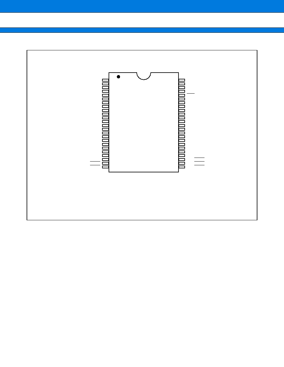
PIN ASSIGNMENTS
(Continued)
(TOP VIEW)
(DIP-48P-M01)
*1 : For pin no. 2, connect this pin to an external 0.1
µ
F capacitor to ground (for MB89P475 only) .
For MB89PV470 and MB89475, this pin should be left unconnected.
*2 : High current drive type
V
SS
C*
1
P40/X0A
P41/X1A
P17/TO2
P16/EC2
P15/TO1
P14/EC1
P13/INT13
P12/INT12
P11/INT11
P10/INT10
P07/AN7
P06/AN6
P05/AN5
P04/AN4
P03/AN3
P02/AN2
P01/AN1
P00/AN0
AV
SS
AV
CC
P54/INT24
P53/INT23
1
2
3
4
5
6
7
8
9
10
11
12
13
14
15
16
17
18
19
20
21
22
23
24
48
47
46
45
44
43
42
41
40
39
38
37
36
35
34
33
32
31
30
29
28
27
26
25
X1
X0
MODE
P42
RST
P20/SCK1
P21/SO1
P22/SI1
P23/PWC
P24/PWM
P25/SI2
V
CC
P26/SO2
P27/SCK2
P30/BUZ*
2
P31*
2
P32*
2
P33*
2
P34*
2
P35*
2
P36*
2
P50/INT20
P51/INT21
P52/INT22