DS07-12555-1E
FUJITSU SEMICONDUCTOR
DATA SHEET
8-bit Proprietary Microcontroller
CMOS
F
2
MC-8L MB89560A Series
MB89567A/567AC/P568/PV560
s
DESCRIPTION
The MB89560A series has been developed as a general-purpose version of the F
2
MC*
1
-8L family consisting of
proprietary 8-bit, single-chip microcontrollers.
In addition to a compact instruction set, the microcontroller contains a variety of peripheral functions such as I
2
C
interface*
2
, timers, 2 ch 8-bit PWM timers, 8/16-bit timer, 21-bit timebase timer, 8-bit PWC timer, 17-bit Watch
prescaler, Watch-dog timer, High speed UART, 8-bit SIO, UART/SIO, LCD controller/driver (optional booster),
Two type Programmable Pulse Generators (PPG), an A/D converter, and external interrupt.
*1 : F
2
MC stands for FUJITSU Flexible Microcontroller.
*2 : I
2
C of this product is complied to Intel Corp. System Management Bus Rev. 1.0 specification and to the Philips
I
2
C specification.
s
FEATURES
∑ F
2
MC-8L family CPU core
∑ Low-voltage operation (when an A/D converter is not used)
∑ Low current consumption (applicable to the dual-clock system)
∑ Minimum execution time: 0.32
µ
s at 12.5 MHz /3.5 V to 5.5 V
(Continued)
s
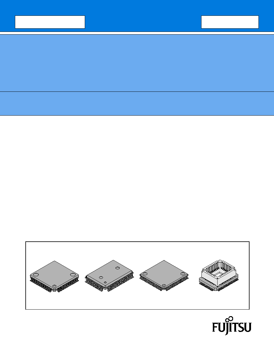
PACKAGES
80-pin Plastic LQFP
80-pin Plastic QFP
80-pin Plastic LQFP
80-pin Ceramic MQFP
FPT-80P-M05
FPT-80P-M06
FPT-80P-M11
MQP-80C-P01

MB89560A Series
2
(Continued)
∑ I
2
C interface circuit
∑ LCD controller/driver: 24 segments x 4 commons (Max 96 pixels, duty LCD mode and Static LCD mode)
∑ LCD booster function (option)
∑ Wild register (Max 6 different address locations)
∑ 10-bit A/D converter: 8 channels
∑ Three types of Serial Interface:
High Speed UART (
Transfer rate from 300 bps to 192000 bps /10 MHz main clock)
8-bit Serial I/O (SIO)
UART/SIO
∑ Two type of Programmable Pulse Generator(PPG): 6-bit PPG and 12-bit PPG
∑ Six types of timer
8-bit PWM 2 channels timers
8/16-bit timer/counter (8 bits x 2 channels or 16 bits x 1 channel)
21-bit timebase timer
8-bit PWC timer operation
17-bit Watch prescaler
Watch-dog timer
∑ I/O ports: Max 50 channels
∑ External interrupt 1: 8 channels
∑ External interrupt 2 (wake-up function): 4 channels
∑ Low-power consumption modes (stop mode, sleep mode, and watch mode)
∑ LQFP-80 and QFP-80 package
∑ CMOS technology
MB89560A Series
3
s
PRODUCT LINEUP
(Continued)
Part number
Parameter
MB89567A
MB89567AC
MB89P568
MB89PV560
Classification
Mass production products
(mask ROM products)
OTP
Piggy-back
ROM size
32 K x 8-bit
(internal mask ROM)
48 K x 8-bit
(internal PROM)
56 K x 8-bit
(external ROM)
RAM size
1 K x 8-bit
1 K x 8-bit
CPU functions
Number of instructions
: 136
Instruction bit length
: 8-bit
Instruction length
: 1 to 3 bytes
Data bit length
: 1-, 8-, 16-bit
Minimum execution time
: 0.32
µ
s/12.5 MHz
Minimum interrupt processing time
: 2.88
µ
s/12.5 MHz
Ports
General-purpose I/O ports (N-channel open drain): 20 pins (2 shared with I
2
C inputs,
16 shared with LCD, 2 shared with other
resources)
General-purpose I/O ports (CMOS)
: 30 pins (shared with resources)
Total
: 50 pins
21-bit timebase
timer
21-bit
Interrupt cycle: (2
13
, 2
15
, 2
18
or 2
22
)/F
CH
*
7
Watchdog timer
Reset generate cycle: Min 2
21
/F
CH
*
7
for main clock, Min 2
14
/F
CL
*
7
for sub clock
Watch prescaler
17-bit
Interrupt cycle: 31.25 ms, 0.25 s, 0.50 s, 1.00 s, 2.00 s, 4.00 s/32.768 kHz for subclock
8/16-bit timer/
counter
Can be operated either as a 2-channel 8-bit timer/counter (Timer 1 and Timer 2, each with its
own independent operating clock cycle), or as one 16-bit timer/counter
In Timer 1 or 16-bit timer/counter operation, event counter operation (external clock-triggered)
and square wave output capable
8-bit PWM 2 ch
timer
8-bit interval timer operation (square wave output capable, operating clock cycle: 1 t
inst
, 8 t
inst
,
16 t
inst
, 64 t
inst
)
8-bit resolution PWM operation (conversion cycle: 128 x 1 t
inst
to 256 x 64 t
inst
)
8/16-bit timer/counter output for counter clock selectability
PWC timer
8-bit timer operation (count clock cycle: 1 t
inst
, 4 t
inst
, 32 t
inst
)
8-bit reload timer operation (toggle output possible, operating clock cycle: 1 to 32 t
inst
)
8-bit pulse width measurement (continuous measurement possible: H-width, L-width, rising
edge to rising edge, falling edge to falling edge, and rising edge to falling edge)
10-bit A/D
converter *
2
10-bit resolution ◊ 8 channels
A/D conversion function (conversion time: 60 t
inst
)
Continuous activation by an 8/16-bit timer/counter output or a timebase timer output capable.
6-bit PPG
Internal 6-bit counter
Pulse width and cycle are program selectable
12-bit PPG
Internal 12-bit counter
Pulse width and cycle are program selectable
MB89560A Series
4
(Continued)
*1 : When booster is used, the bias is reduced by 1/3. It can be selected by mask option.
*2 : Voltage varies with product.
*3 : When external ROM is used, EPROM: MBM27C512-20 should be used, the operating voltage: 4.5 V to 5.5 V.
*4 : I
2
C is complied to Intel Corp. System Management Bus Rev. 1.0 specification and to the Philips I
2
C specification.
*5 : 1 t
inst
= one instruction cycle (execution time) which can be selected as 1/4, 1/8, 1/16, or 1/64 of main clock
if main clock mode is selected, or 1/2 of the subclock if subclock mode is selected.
*6 : Varies with conditions such as the operating frequency. (See "
s
ELECTRICAL CHARACTERISTICS.")
*7 : F
CH
: main clock source oscillation, F
CL
: sub clock source oscillation
Part number
Parameter
MB89567A
MB89567AC
MB89P568
MB89PV560
I
2
C interface*
4
Not
Available
1 channel
High speed UART
Transfer data length: 4-, 6-, 7-, 8-bit
Transfer rate (300 bps to 192000 bps /9.216 MHz main clock)
support sub-clock mode
UART/SIO
Transfer data length: 7-, 8-bit for UART, 8-bit for SIO
Transfer rate (1201 bps to 78125 bps / 10 MHz main clock)
support sub-clock mode
8-bit serial I/O
8-bit, LSB first/MSB first selectability
Transfer clocks (one external shift clock, three internal shift clocks: 2 t
inst
, 8 t
inst
, 32 t
inst
) *
5
LCD
Common output: 4 (Max)
Segment output: 24 (Max)
LCD driving power (bias) pins: 4
LCD display RAM size: 12 bytes (24 ◊ 4 bits, Max 96 pixels)
Duty LCD mode and Static LCD mode
Booster for LCD driving: option*
1
Dividing resistor for LCD driving: option
Wild register
Maximum of 6-byte data can be assigned in 6 different address.
Used to replace any data in the ROM when specific address and data are assigned in Wild
register.
Wild register can be set up by using different communication methods through the device.
External interrupt
1 (wake-up
function)
8 independent channels (interrupt vector, request flag, request output enable)
Edge selectability (rising/falling)
Used also for wake-up from stop/sleep mode. (edge detection is also permitted in stop mode.)
External interrupt
2 (wake-up
function)
4 channels ("L" level interrupts, independent input enable).
Used also for wake-up from stop/sleep mode. (Low-level detection is also permitted in stop
mode.)
Standby mode
Sub clock mode, sleep mode, stop mode and clock mode
Process CMOS
Operating voltage *
6
2.2 V to 5.5 V
2.7 V to 5.5 V
2.7 V to 5.5 V*
3
MB89560A Series
5
s
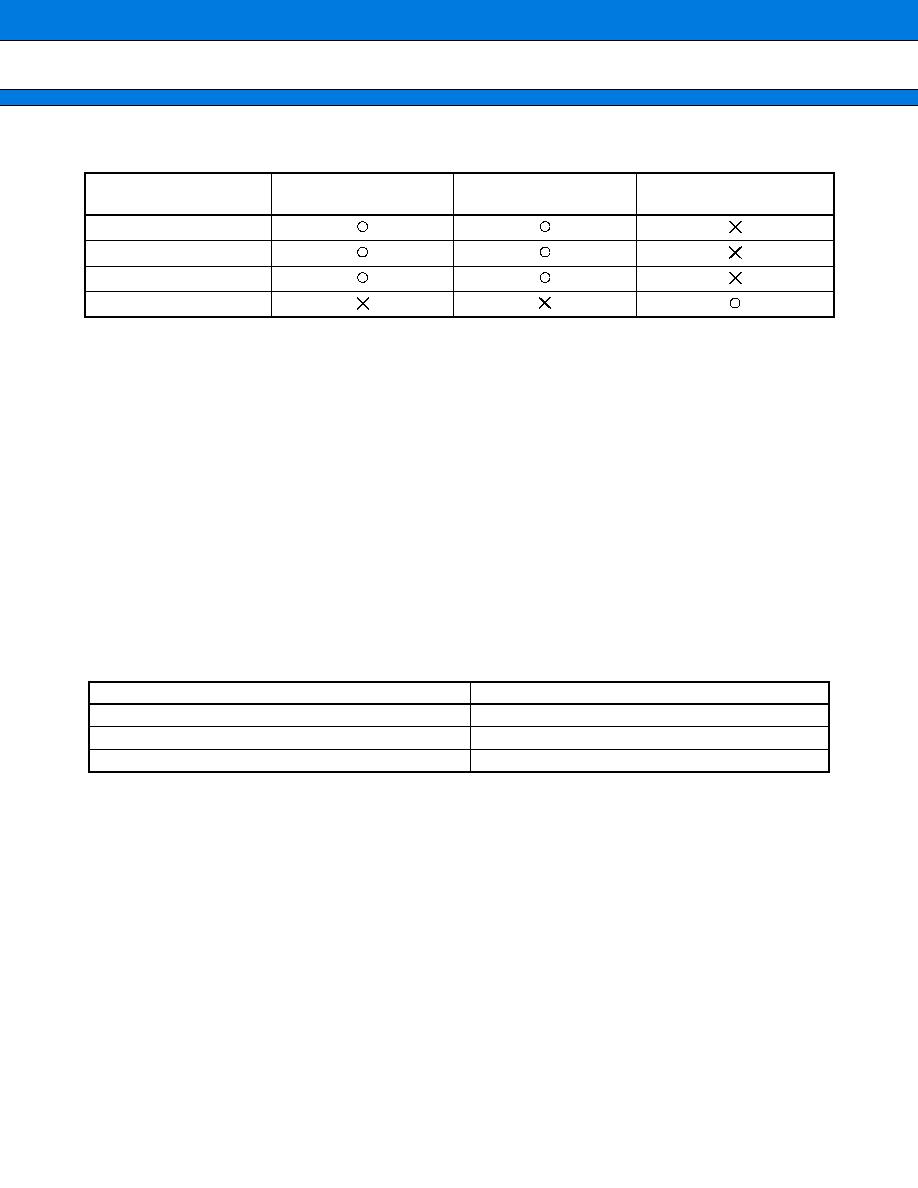
PACKAGE AND CORRESPONDING PRODUCTS
s
DIFFERENCES AMONG PRODUCTS
1.
Memory Size
Before evaluating using the OTPROM (one-time PROM) products, verify its differences from the product that
will actually be used. Take particular care on the following points:
∑ The stack area, etc., is set at the upper limit of the RAM.
2.
Current Consumption
∑ For the MB89PV560, add the current consumed by the EPROM mounted in the piggy-back socket.
∑ When operating at low speed, the current consumed by the one-time PROM product is greater than that for
the mask ROM product. However, the current consumption is roughly the same in sleep or stop mode.
∑ For more information, see "
s
ELECTRICAL CHARACTERISTICS."
3.
Mask Options
The functions available as options and the method of specifying options differ between products.
Before using options check "
s
MASK OPTIONS."
4.
Wild register function
The Wild Register can be used in the following address spaces.
5.
P40, P41
It will take about 64 count clock of external oscillation to initialize P40 and P41 pins in MB89PV560/P568.
Therefore, these ports will be unstable for a while during power-on. For MB89567A/567AC, these ports will be
in High-Z during power-on.
Package
MB89567A
MB89567AC
MB89P568-101
MB89P568-102
MB89PV560-101
MB89PV560-102
FPT-80P-M05
FPT-80P-M06
FPT-80P-M11
MQP-80C-P01
Device
Address Space
MB89PV560
4000
H
to FFFF
H
MB89P568
4000
H
to FFFF
H
MB89567A/567AC
8000
H
to FFFF
H