DS07-12544-2E
FUJITSU SEMICONDUCTOR
DATA SHEET
8-bit Proprietary Microcontrollers
CMOS
F
2
MC-8L MB89590B/BW Series
MB89593B/595B/P595B/
MB89593BW/595BW/P595BW
s
s
s
s
DESCRIPTION
The MB89590B/BW series is a line of general-purpose, single-chip microcontrollers. In addition to a compact in-
struction set, these microcontrollers contain a variety of peripheral functions, such as PLL clock control, timers, a
serial interface, a PWM timer, the USB hub function, and the USB function. The USB hub function, in particular, sup-
ports five ports (one of them is dedicated to an internal function) allowing them to interface with other USB devices.
The microcontrollers also contain one USB function channel to support high speeds.
s
s
s
s
FEATURES
� Package type
64-pin LQFP package (0.5 mm pitch)
� High-speed operations at low voltage
Minimum execution time : 0.33
�
s (Automatically generates a 12 MHz main clock and a 48 MHz USB interface
synchronization clock with an externally supplied 6 MHz clock and the internal PLL circuit.)
� F
2
MC-8L CPU core
Instruction set that is optimum to the controllers
Multiplication and division instructions,
16-bit arithmetic operations,
Branch instructions by bit testing,
Bit manipulation instructions, etc.
(Continued)
s
s
s
s
PACKAGE
64-pin plastic LQFP
(FPT-64P-M03)

MB89590B/BW Series
2
(Continued)
� PLL clock control
The internal PLL clock circuit allows the use of low-speed clocks which are advantageous to noise character-
istics.
(6 MHz externally supplied clock : Internal system clock oscillated at 12 MHz)
� Various timers
8-bit PWM timer (can be used as either 8-bit PWM timer
�
2 channels or PPG timer
�
1 channel)
Internal 21-bit timebase timer
� Internal USB transceiver circuit (Compatible with high and low speeds)
� USB hub
Compliant to USB Protocol Revision 1.0
Five downstream port channels (One of these channels is dedicated to a function.)
Automatically responds to all USB protocols by hardware.
Descriptor configuration information is provided as ROM data for automatic responding by hardware (vendor
ID and product ID) .
* String data is not supported.
Allows switching between BUS power supply and own power supply modes.
Power supply to the USB down ports is controlled port by port.
� USB function
Compliant to USB Protocol Revision 1.0
Support for full speed
Allows four endpoints to be specified at maximum.
Types of transfer supported : control/interrupt/bulk/isochronous
Built-in DMAC (Maps the buffer for each endpoint on to the internal RAM to directly access the memory for
function's send and receive data.)
� UART/serial interface
Built-in UART/SIO function (selectable by switching)
� External interrupt
External interrupt (level detection
�
8 channels)
Eight inputs are independent of one another and can also be used for resetting from low-power consumption
mode (the L-level detection feature available) .
� Low power consumption (standby mode supported)
Stop mode (There is almost no current consumption since oscillation stops.)
Sleep mode (This mode stops the running CPU.)
� A maximum of 45 general-purpose I/O ports
General-purpose I/O ports (CMOS) : 34
General-purpose output ports (CMOS) : 8
General-purpose I/O ports (Nch open drain) : 3
� Power supply
Supply voltage : 3.0 to 5.5 V
MB89590B/BW Series
3
s
s
s
s
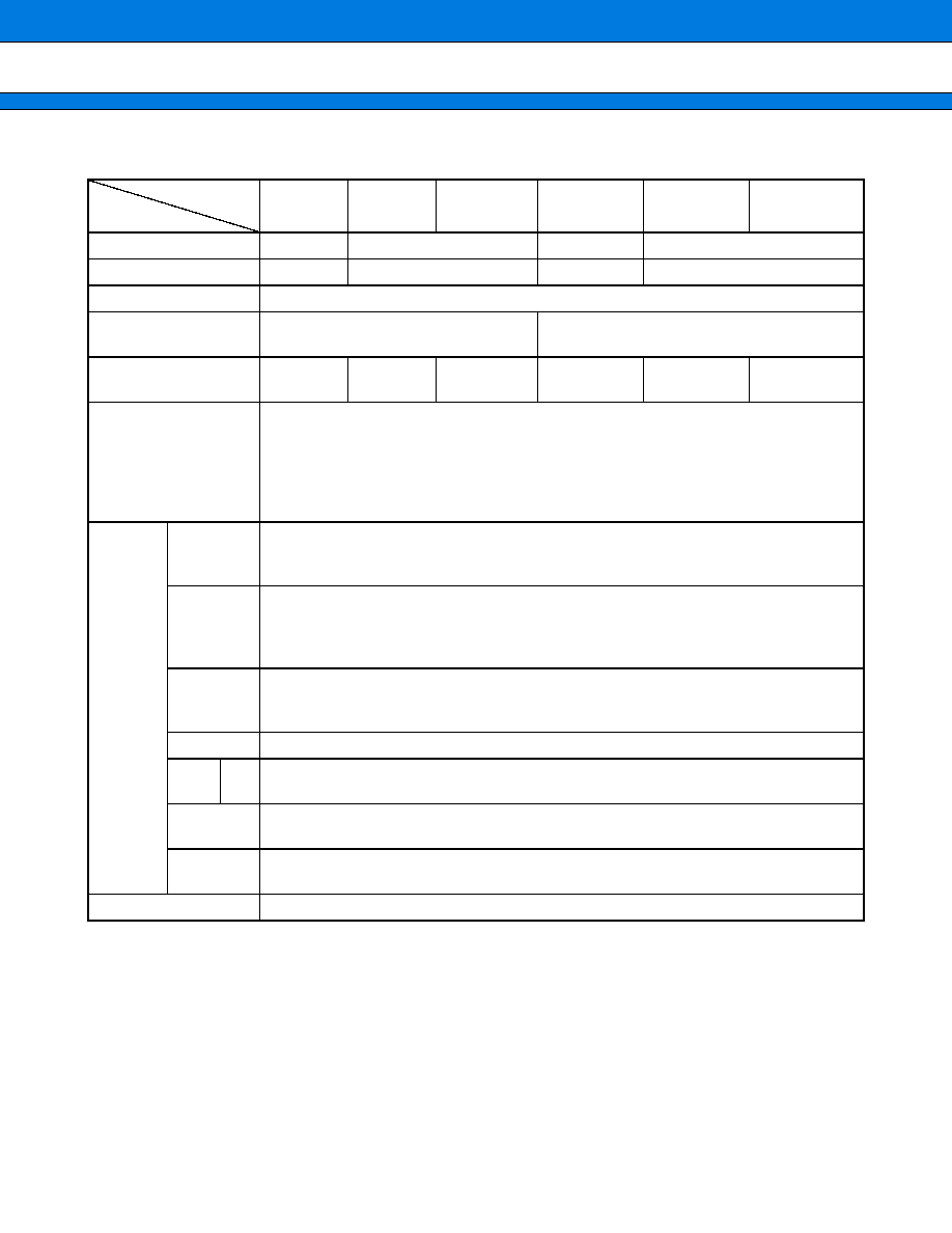
PRODUCT LINEUP
Part number
MB89593B MB89595B MB89P595B MB89593BW MB89595BW MB89P595BW
Parameter
ROM size
8 KB
16 KB
8 KB
16 KB
RAM size
512 B
1 KB
512 B
1 KB
Package
LQFP-64 (FPT-64P-M03)
Operation
at USB reset
High impedance state
Low-level output
Others
MASK
product
MASK
product
OTP/EVA
product
MASK
product
MASK
product
OTP/EVA
product
CPU functions
Number of instructions
Instruction bit length
Instruction length
Data bit length
Minimum execution time
Interrupt processing time
: 136
: 8 bits
: 1 to 3 bytes
: 1, 8, and 16 bits
: 0. 33
�
s (6 MHz)
: 3
�
s (6 MHz)
Peripher-
al func-
tions
General-
purpose
ports
General-purpose I/O ports
General-purpose output ports
(34 : CMOS; 3 : Nch open drain)
(8 : CMOS)
USB hub
Upstream port : 1 channel
Downstream port : 5 channels (One is dedicated to an internal function.)
Port power supply control method : By individual port
Allows selection between own power supply and bus power supply
USB
function
Supports full speed.
Four endpoints at maximum
Built-in DMAC (Allows DMA transfer to the internal RAM)
PWM timer
8-bit PWM timer operation
�
2 channels (can also be used as a PPG
�
1 channel timer)
UART SIO
Allows switching between UART (clock-synchronous/asynchronous data transfer al-
lowed) and SIO (simple serial transfer) .
Timebase
timer
21-bit timebase timer
Clock
output
Allows output of two main clock divisions
Standby mode
Sleep mode and Stop mode
MB89590B/BW Series
4
s
s
s
s
DIFFERENCES AMONG PRODUCTS
1.
Memory Size
Before evaluating using the OTP product, verify its differences from the product that will actually be used.
2.
Current Consumption
When operated at low speeds, a product mounted with either one-time PROM or EPROM consumes more
current than a product mounted with a mask ROM. However, in sleep/stop mode the current consumption is the
same.
For detailed information on each package, see "
s
PACKAGE DIMENSIONS."
3.
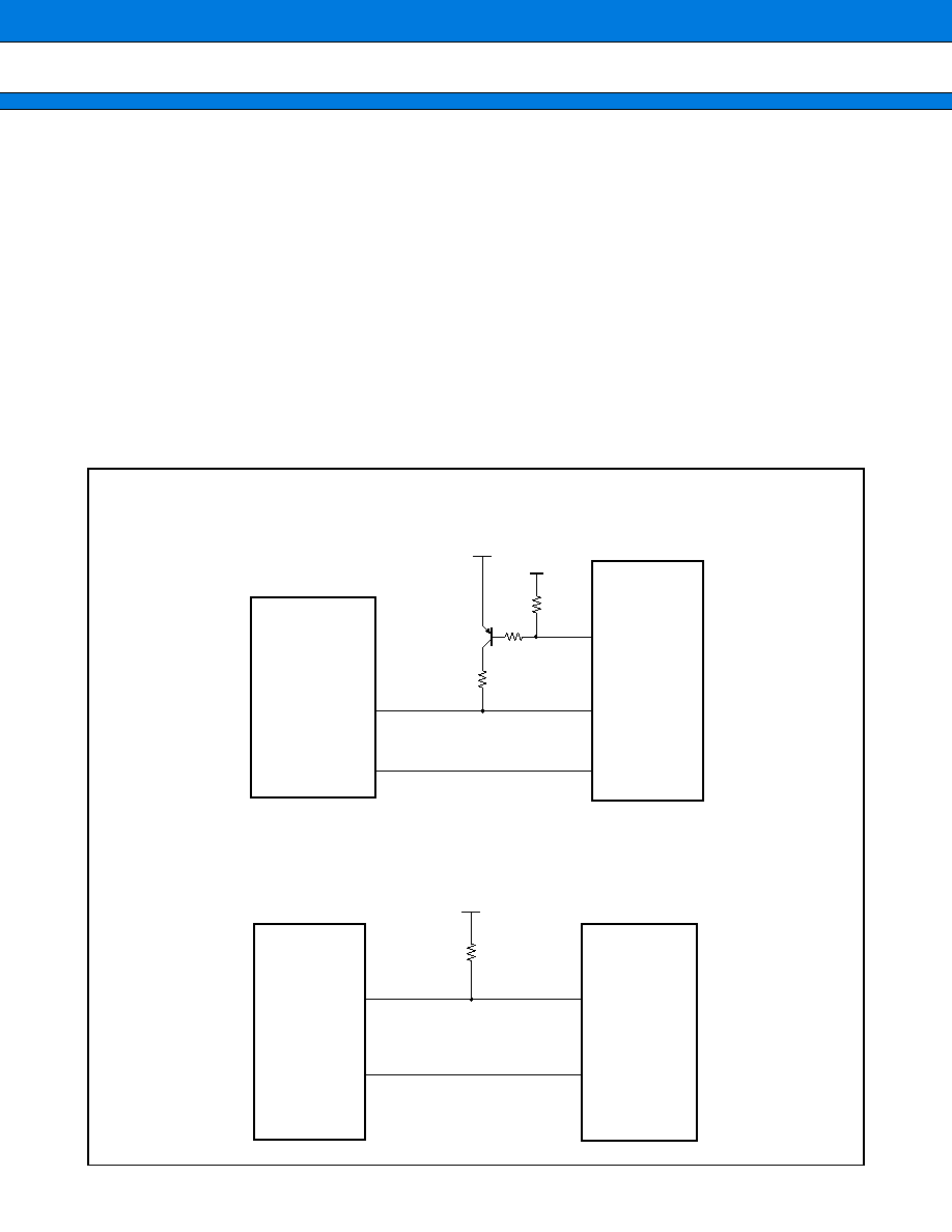
Differences Between the MB89590B series and the MB89590BW Series
MB89590B series :
Remains in high impedance state until USB connection takes place. Before the USB
connection, use one general-purpose port output to control pullup resistance connec-
tion of this port by software.
MB89590BW series : Outputs at low level until USB connection takes place.
D
+
D
-
1.5 k
3.3 V
General-purpose
port
RPVP pin
RPVM pin
Host PC
MB89590B series
� Example MB89590B product connection
D
+
D
-
1.5 k
3.3 V
RPVP pin
RPVM pin
Host PC
MB89590BW series
� Example MB89590BW product connection
MB89590B/BW Series
5
s
s
s
s
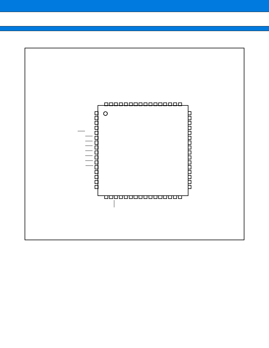
PIN ASSIGNMENT
(TOP VIEW)
(FPT-64P-M03)
P44/UCK
P45/UO
P46/UI/PWM1
P47/PWM2
P30/INT0/CLK
P31/INT1
P32/INT2
P33/INT3
P34/INT4
P35/INT5
P36/INT6
P37/INT7
P50
V
SS
P51
P52
1
2
3
4
5
6
7
8
9
10
11
12
13
14
15
16
P00
P01
P02
P03
P04
P05
P06
P07
P10
P11
P12
P13
P14
P15
P16
P17
48
47
46
45
44
43
42
41
40
39
38
37
36
35
34
33
P53
P54
RST
MOD0
MOD1
X0
X1
V
SS
P27
P26
P25
P24
P23
P22
P21
P20
17
18
19
20
21
22
23
24
25
26
27
28
29
30
31
32
P43/POW4
P42/POW3
P41/POW2
P40/POW1
D4VM
D4VP
D3VM
D3VP
D2VM
D2VP
D1VM
D1VP
RPVM
RPVP
C
V
CC
64
63
62
61
60
59
58
57
56
55
54
53
52
51
50
49