DS07-12526-1E
FUJITSU SEMICONDUCTOR
DATA SHEET
8-bit Proprietary Microcontroller
CMOS
F
2
MC-8L MB89920 Series
MB89923/925/P928/PV920
s
DESCRIPTION
The MB89920 series is a line of single-chip microcontrollers using the F
2
MC*-8L CPU core which can operate
at low voltage but at high speed.
The microcontrollers in this series contain peripheral functions such as a PWM timer, an input capture/output
compare control counter, an LCD controller/driver, an A/D converter, and a UART.
The MB89920 series can suit a wide range of applications such as analog input conversion, pulse input
measurement/pulse output control, serial communications control, and display control.
*: F
2
MC stands for FUJITSU Flexible Microcontroller.
s
FEATURES
∑ High speed processing at low voltage
Minimum execution time: 0.5
µ
s/8.0 MHz
∑ F
2
MC-8L family CPU core
∑ 8-bit PWM timer: 2 channels (also usable as a reload timer)
∑ 16-bit input capture: 2 channels / 16-bit output compare: 2 channels
(Continued)
s
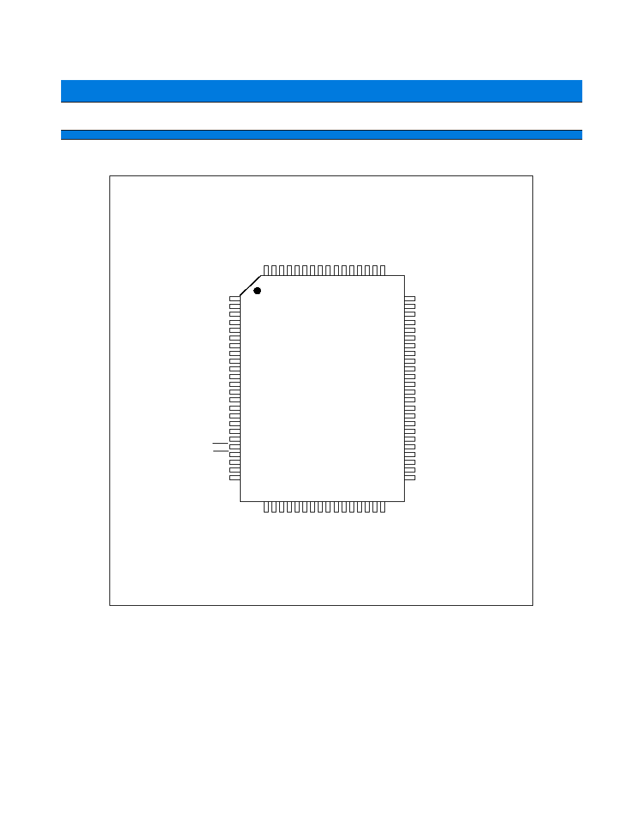
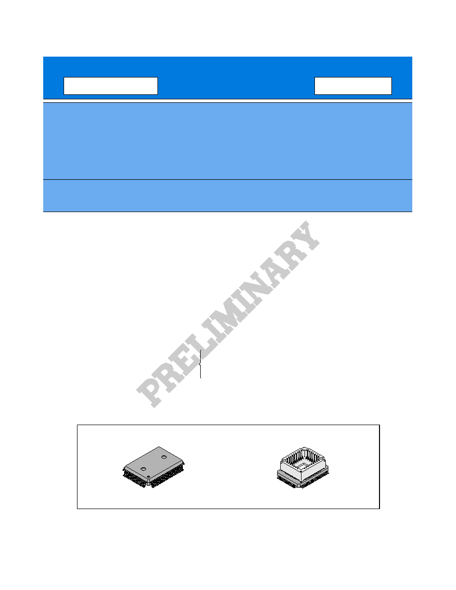
PACKAGE
Multiplication and division instructions
16-bit arithmetic operations
Test and branch instructions
Bit manipulation instructions, etc.
Instruction set optimized for controllers
(MQP-80C-P01)
(FPT-80P-M06)
80-pin Plastic QFP
80-pin Ceramic MQFP

2
MB89920 Series
(Continued)
∑ 20-bit time-base counter
∑ UART: 1 channel (with asynchronous transfer mode and 8-bit synchronous serial mode)
∑ 8-bit serial interface: 1 channel (LSB first/MSB first selectability)
∑ 10-bit A/D converter: 8 channels
∑ LCD controller/driver: 28 segments
◊
4 commons (max. 112 pixels)
∑ Low-voltage detection reset
∑ Watchdog timer reset
∑ External interrupt: 4 channels
Four channels are independent and capable of wake-up from the low-power consumption mode (with edge
detection function)
∑ Buzzer output/clock output
∑ Low-power consumption modes:
Stop mode (The software stops oscillation to minimize the current consumption.)
Sleep mode (The CPU stops to reduce current consumption to approx. 1/3 of normal.)
Hardware standby mode (The pin input stops oscillation.)
3
MB89920 Series
s
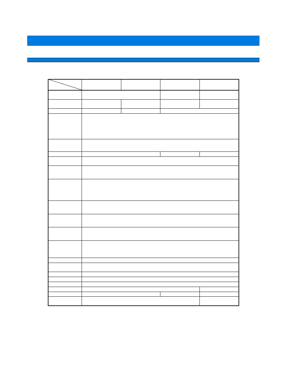
PRODUCT LINEUP
* : The minimum operating voltage varies with conditions such as the operating frequencies, functions, and
development tool.
MB89925
MB89P928
MB89PV920
Classification
Mass production products
(mask ROM products)
One-time PROM product
(for development)
Piggyback/evaluation
product (for development)
ROM size
8 K
◊
8 bits
(internal mask ROM)
16 K
◊
8 bits
(internal mask ROM)
48 K
◊
8 bits
(internal PROM)
48 K
◊
8 bits
(external ROM)
RAM size
256
◊
8 bits
512
◊
8 bits
1024
◊
8 bits
CPU functions
Number of instructions:
136
Instruction bit length:
8 bits
Instruction length:
1 to 3 bytes
Data bit length:
1, 8, 16 bits
Minimum execution time:
0.5
µ
s/8 MHz
Interrupt processing time:
4.5
µ
s/8 MHz
Ports
I/O ports (CMOS):
35 (25 ports also serve as peripherals.)
I/O ports (N-ch open-drain):
34 (All also serve as peripherals.)
Total:
69
Options
Specify with mask options
Set with EPROM programmer
None
20-bit time-base
timer
20 bits (interval time selection: 4.10 ms, 16.38 ms, 65.54 ms, 262 ms/8 MHz)
Real-time I/O
16-bit timer: operating clock cycle (0.5
µ
s, 1.0
µ
s, 2.0
µ
s, 4.0
µ
s), overflow interrupt
Input capture: 16 bits
◊
2 channels, external trigger edge selectability
Output compare: 16 bits
◊
2 channels
LCD controller/
driver
Common output: 4 (selectable from 2 to 4 by software)
Segment output: 28 (can be switched to ports in 4-pin unit by software)
Bias power supply pins: 3
LCD display RAM size: 14
◊
8 bits
Dividing resistor for LCD driving: bult-in (external resistor selectability)
8-bit PWM timer
8 bits
◊
2-channel reload timer operation
8 bits
◊
2-channel PWM operation (4 cycles selectable)
8 bits
◊
1-channel PPG operation (4 oscillation clocks selectable)
UART
Variable data length (7 or 8 bits), internal baud rate generator, error detection function,
full-duplex with internal double buffer, NRZ transmission formation,
Clock synchronous/asynchronous transfer capable
8-bit serial I/O
8 bits, LSB first/MSB first selectability,
One clock selectable from four transfer clocks
(one external shift clock, three internal shift clocks: 1.0
µ
s, 4.0
µ
s, 16.0
µ
s)
10-bit A/D
converter
10-bit resolution
◊
8 channels
A/D conversion mode (conversion time: 16.5
µ
s (33 instruction cycles))
Sense mode (conversion time: 9.0
µ
s (18 instruction cycles))
Continuous activation by an internal clock capable
Watchdog timer
Interval time: approx. 130 to 260 ms
Low-voltage
detection reset
Reset activation voltage: 3.0 to 4.3 V
Reset release voltage: 3.1 to 4.5 V
Hardware standby
Stop the clock oscillation by pin input
Buzzer/clock output
1 channel (output a frequency from 1 KHz, 2 KHz, 4 KHz, and divided clock frequency)
External interrupt
4 channels (rising edge/falling edge selectability)
Package
QFP-80
MQFP-80
Operating voltage
2.2 to 6.0 V*
2.7 to 6.0 V*
2.7 to 6.0 V*
EPROM for use
MBM27C512-20TV
(LCC package)
MB89923
Part number
Parameter
4
MB89920 Series
s
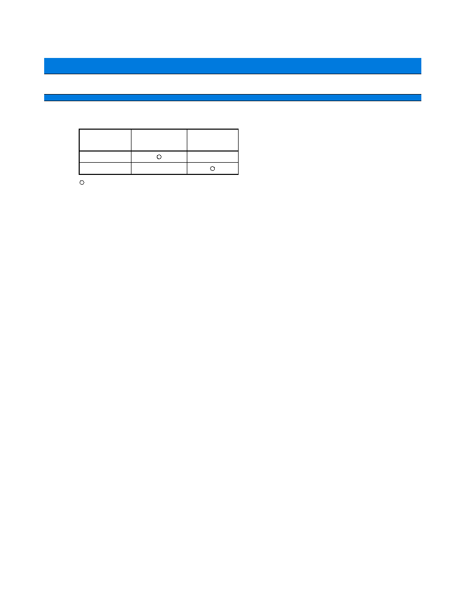
PACKAGE AND CORRESPONDING PRODUCTS
: Available
◊
: Not available
Note: For more information about each package, see section "
s
Package Dimensions."
s
DIFFERENCES AMONG PRODUCTS
1. Memory Size
Before evaluating using the piggyback product, verify its differences from the product that will actually be used.
Take particular care on the following points:
∑ The stack area, etc., is set at the upper limit of the RAM.
∑ The external area is used.
2. Current Consumption
∑ In the case of the MB89PV920, add the current consumed by the EPROM which is connected to the top socket.
∑ When operated at low speed, the product with an OTPROM (one-time PROM) or an EPROM will consume
more current than the product with a mask ROM.
However, the current consumption in sleep/stop modes is the same. (For more information, see section
"
s
Electrical Characteristics.")
3. Mask Options
Functions that can be selected as options and how to designate these options vary by the product.
Before using options check section "
s
Mask Options."
Package
MB89923
MB89925
MB89P928
MB89PV920
FPT-80P-M06
◊
MQP-80C-P01
◊