 | ÐлекÑÑоннÑй компоненÑ: MB89PV490 | СкаÑаÑÑ:  PDF PDF  ZIP ZIP |
Äîêóìåíòàöèÿ è îïèñàíèÿ www.docs.chipfind.ru
1
Revision 1.5
FUJITSU SEMICONDUCTOR
DATA SHEET
PR
ELIM
INA
R
Y
8-bit Proprietary Microcontroller
CMOS
F
2
MC-8L MB89490 Series
MB89497/498/F499/PV490
DESCRIPTION
The MB89490 series has been developed as a general-purpose version of the F
2
MC*-8L family consisting of
proprietary 8-bit single-chip microcontrollers.
In addition to a compact instruction set, the microcontroller contains a variety of peripheral functions such as
21-bit timebase timer, watch prescaler, PWM timer, 8/16-bit timer/counter, remote receiver control, LCD
controller/driver, external interrupt 0 (edge), external interrupt 1 (level), 10-bit A/D converter, UART/SIO, SIO,
I
2
C and watchdog timer reset.
The MB89490 series is designed suitable for compact disc/cassette tape/radio receiver controller as well as in
a wide range of applications for consumer product.
*: F
2
MC stands for FUJITSU Flexible Microcontroller.
FEATURES
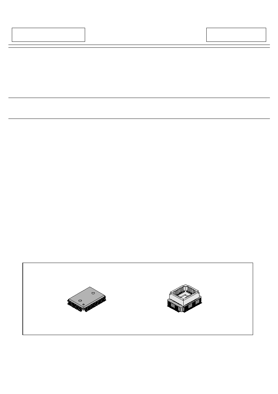
· Package used
QFP package for MB89F499, MB89497,MB89498
MQFP package for MB89PV490
· High speed operating capability at low voltage
· Minimum execution time: 0.32
µ
s/12.5MHz
(Continued)
PACKAGE
(FPT-100P-M06)
(FTP-100P-M06)
100-pin Plastic QFP
(MQP-100C-P01)
100-pin Ceramic MQFP

2
MB89490 Series
(Continued)
· F
2
MC-8L family CPU core
· Clock
Embedded PLL clock multiplication circuit for sub-clock
Operating clock (PLL for sub-clock) can be selected four times of the sub-clock oscillation
· Six timers
PWM timer x 2
8/16-bit timer/counter x 2
21-bit timebase timer
Watch prescaler
· External interrupt
Edge detection (selectable edge) : 8 channels
Low level interrupt (wake-up function) : 8 channels
· 10-bit A/D converter (8 channels)
10-bit successive approximation type
· UART/SIO
Synchronous/asynchronous data transfer capability
· SIO
Synchronous data transfer capability
· LCD controller/driver
Max. 32 segments output x 4 commons
· I
2
C interface circuit
· Remote receiver circuit
· Low-power consumption mode
Stop mode (oscillation stops so as to minimize the current consumption.)
Sleep mode (CPU stops so as to reduce the current consumption to approx. 1/3 of normal.)
Watch mode (everything except the watch prescaler stops so as to reduce the power comsumption to an
extremely low level.)
Sub-clock mode
· Watchdog timer reset
· I/O ports: max. 66channels
PRODUCT LINEUP
MB89497
MB89498
MB89F499
MB89PV490
Classification
Mass production products
(mask ROM product)
FLASH
Piggy-back
ROM size
32K x 8-bit
(internal ROM)
48K x 8-bit
(internal ROM)
60K x 8-bit (internal FLASH)
60K x 8-bit (external ROM)*
1
RAM size
1K x 8-bit
2K x 8-bit
2K x 8-bit
2K
×
8-bit
*1 : Use MBM27C512 as the external ROM.
Multiplication and division instructions
16-bit arithmetic operations
Test and branch instructions
Bit manipulation instructions, etc.
Instruction set optimized for controllers
Part number
Parameter
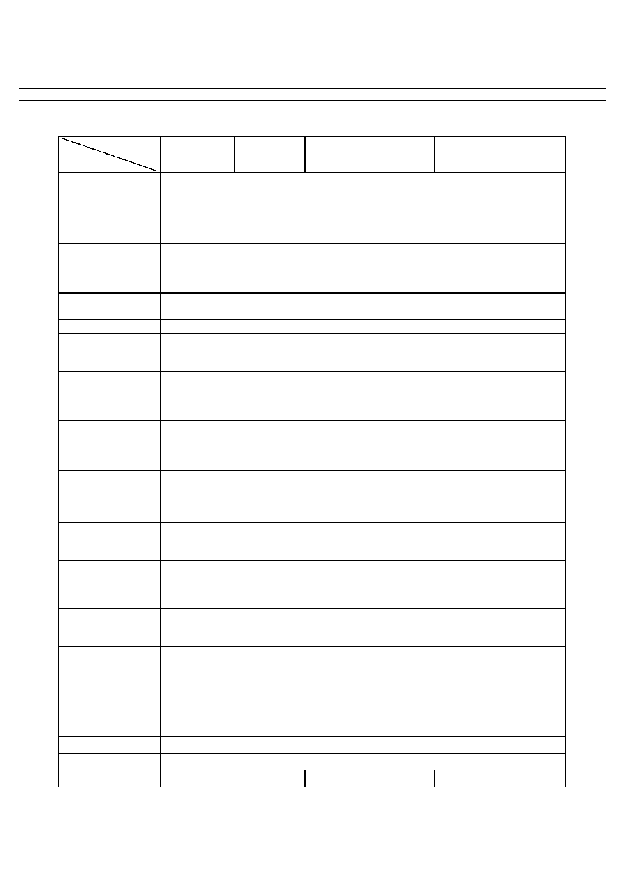
3
MB89490 Series
*1 : I
2
C is complied to Philips I
2
C specification.
MB89497
MB89498
MB89F499
MB89PV490
CPU functions
Number of instructions
: 136
Instruction bit length
: 8 bits
Instruction length
: 1 to 3 bytes
Data bit length
: 1, 8, 16 bits
Minimum execution time
: 0.32
µ
s/12.5 MHz
Minimum interrupt processing time
: 2.88
µ
s/12.5 MHz
Ports
I/O ports (CMOS)
: 56 pins
Input ports (CMOS)
: 2 pins
N-channel open drain I/O ports
: 8 pins
Total
: 66 pins
21-bit timebase
timer
Interrupt period (0.66 ms, 2.6 ms, 21.0 ms, 335.5 ms) at 12.5 MHz
Watchdog timer
Reset period (167.8 ms to 335.5 ms) at 12.5 MHz.
PWM timer 0,1
8-bit reload timer operation (supports square wave output, operating clock period: 1, 8, 16, 64
t
inst
,)
8-bit resolution PWM operation
8/16-bit timer/
counter 00, 01
Can be operated either as a 2-channel 8-bit timer/counter (timer 00 and timer 01, each with its
own independent operating clock cycle), or as one 16-bit timer/counter
In timer 00 or 16-bit timer/counter operation, event counter operation (external clock-triggered)
and square wave output capability
8/16-bit timer/
counter 10, 11
Can be operated either as a 2-channel 8-bit timer/counter (timer 10 and timer 11, each with its
own independent operating clock cycle), or as one 16-bit timer/counter
In timer 10 or 16-bit timer/counter operation, event counter operation (external clock-triggered)
and square wave output capability
External interrupt 0
(edge)
8 independent channels (selectable edge, interrupt vector, request flag)
External interrupt 1
(level)
8 channels (low level interrupt)
A/D converter
10-bit resolution
×
8 channels
A/D conversion function (conversion time: 38 t
inst
)
Supports repeated activation by internal clock
LCD controller/driver
Common output
: 4 (max.)
Segment output
: 32 (max.)
Bias power supply pins
: 3
LCD display RAM size
: 32
×
4 bits
UART/SIO
Synchronous/asynchronous data transfer capability
(Max. baud rate: 97.656 Kbps at 12.5 MHz)
(7 and 8 bits with parity bit; 8 and 9 bits without parity bit)
SIO
8-bit serial I/O with LSB first/MSB first selectability
One clock selectable from four operation clock (one external shift clock, three internal shift
clock: 0.64
µ
s, 2.56
µ
s, 10.24
µ
s at 12.5MHz)
I
2
C
*1
1 channel
Use a 2-wire protocol to communicate with other device
Remote receiver
Selectable maximum noise width removal
Reversible input polarity
Standby mode
Sleep mode, stop mode, watch mode, sub-clock mode
Process
CMOS
Operating voltage
2.2V ~ 3.6V
2.7V ~ 3.6V
2.7V ~ 3.6V
Part number
Parameter

4
MB89490 Series
PACKAGE AND CORRESPONDING PRODUCTS
O : Availabe
X : Not available
DIFFERENCES AMONG PRODUCTS
1. Memory Size
Before evaluating using the piggyback product, verify its differences from the product that will actually be used.
Take particular care on the following point:
· The stack area is set at the upper limit of the RAM.
2. Current Consumption
· For the MB89PV490 the current consumed by the EPROM mounted in the piggy-back socket is needed to be
included.
· When operating at low speed, the current consumed by the FLASH product is greater than that for the mask
ROM product. However, the current consumption is roughly the same in sleep and stop mode.
· For more information, see "
Electrical Characteristics."
3. Oscillation Stabilization Time after Power-on Reset
· For MB89PV490 and MB89F499, the power-on stabilization time cannot be selected.
· For MB89497 and MB89498, the power-on stabilization time can be selected.
· For more information, please refer to "
Mask Option".
Part number
Package
MB89497/498
MB89F499
MB89PV490
FPT-100P-M06
O
O
X
MQP-100C-P01
X
X
O
5
MB89490 Series
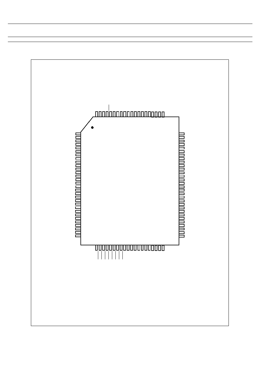
PIN ASSIGNMENT
(
FPT-100P-M06)
Vcc
*P00
*P01
*P02
*P03
*P04
*P05
*P06
*P07
P10/INT00
P11/INT01
P12/INT02
P13/INT03
P14/INT04
P15/INT05
P16/INT06
P17/INT07
P20/TO0
P21/RMC
P22/EC0
P23
P24/TO1
P25/EC1
P26/PWM0
P27/PWM1
P50/SI0
P51/SO0
P52/SCK0
AVR
AVcc
1
2
3
4
5
6
7
8
9
10
11
12
13
14
15
16
17
18
19
20
21
22
23
24
25
26
27
28
29
30
AV
s
s
P3
0
/
AN
0
/
I
N
T
1
0
P3
1
/
AN
1
/
I
N
T
1
1
P3
2
/
AN
2
/
I
N
T
1
2
P3
3
/
AN
3
/
I
N
T
1
3
P3
4
/
AN
4
/
I
N
T
1
4
P3
5
/
AN
5
/
I
N
T
1
5
P3
6
/
AN
6
/
I
N
T
1
6
P3
7
/
AN
7
/
I
N
T
1
7
*P4
0
*P4
1
*P4
2
*P4
3
*P4
4
*P4
5
*
P
46/S
C
L
*P4
7
/
S
D
A
X1
A
X0
A
Vs
s
31
32
33
34
35
36
37
38
39
40
41
42
43
44
45
46
47
48
49
50
P65/SEG21
P64/SEG20
P63/SEG19
P62/SEG18
P61/SEG17
P60/SEG16
SEG15
SEG14
SEG13
SEG12
SEG11
SEG10
SEG9
SEG8
SEG7
SEG6
SEG5
SEG4
SEG3
SEG2
SEG1
SEG0
P54/COM3
P53/COM2
COM1
COM0
V1
V2
V3
Vcc
80
79
78
77
76
75
74
73
72
71
70
69
68
67
66
65
64
63
62
61
60
59
58
57
56
55
54
53
52
51
Vs
s
X0
X1
MO
D
0
RS
T
P8
4
P8
3
P8
2
/
SC
K
1
P8
1
/
SO
1
P8
0
/
SI
1
P7
7
/
SE
G
3
1
P7
6
/
SE
G
3
0
P7
5
/
SE
G
2
9
P7
4
/
SE
G
2
8
P7
3
/
SE
G
2
7
P7
2
/
SE
G
2
6
P7
1
/
SE
G
2
5
P7
0
/
SE
G
2
4
P6
7
/
SE
G
2
3
P6
6
/
SE
G
2
2
10
0
99
98
97
96
95
94
93
92
91
90
89
88
87
86
85
84
83
82
81
(TOP VIEW)
* High current pins
Document Outline