 | ÐлекÑÑоннÑй компоненÑ: MB90091AP | СкаÑаÑÑ:  PDF PDF  ZIP ZIP |
Äîêóìåíòàöèÿ è îïèñàíèÿ www.docs.chipfind.ru
DS04-28823-2E
FUJITSU SEMICONDUCTOR
DATA SHEET
ASSP Image Control
CMOS
Intelligent On-screen Display
Controller (IOSDC)
MB90091A
s
DESCRIPTION
The MB90091A is the multisync, on-screen display controller that supports a variety of TV systems such as
NTSC, PAL, double-scan NTSC, double-scan PAL, 1250HDTV, and 1125HDTV as well as personal computer
monitor display systems such as VGA and XGA.
The MB90091A contains display memory (VRAM) and character font ROM, allowing characters to be displayed
with few external devices. The device also contains command table ROM storing display command data,
minimizing the load on the microcomputer.
The on-screen display configuration is up to 24 characters
×
12 lines, with each character consisting of 24
×
32
dots. The font ROM integrates 512 different character patterns.
The character signal output is an RGB1 digital output. The display color of each character can be specified
from among 16 colors. A color/monochrome select signal output is also provided for display either in 16 different
colors or in 16-level gray scale.
The character display functions include character background display, shaded background display, and sprite
character display functions, contributing to providing colorful display screens.
s
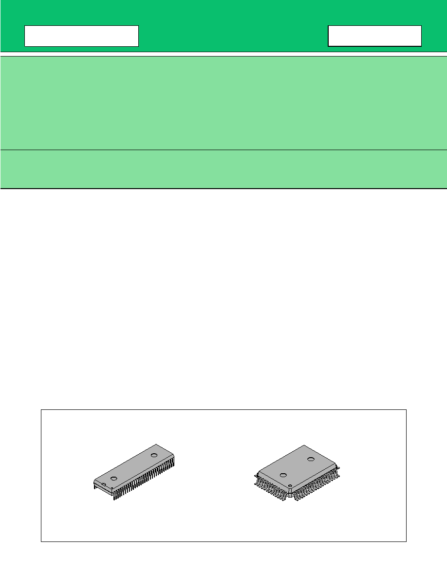
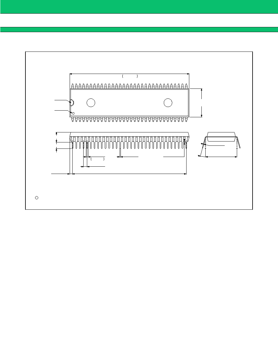
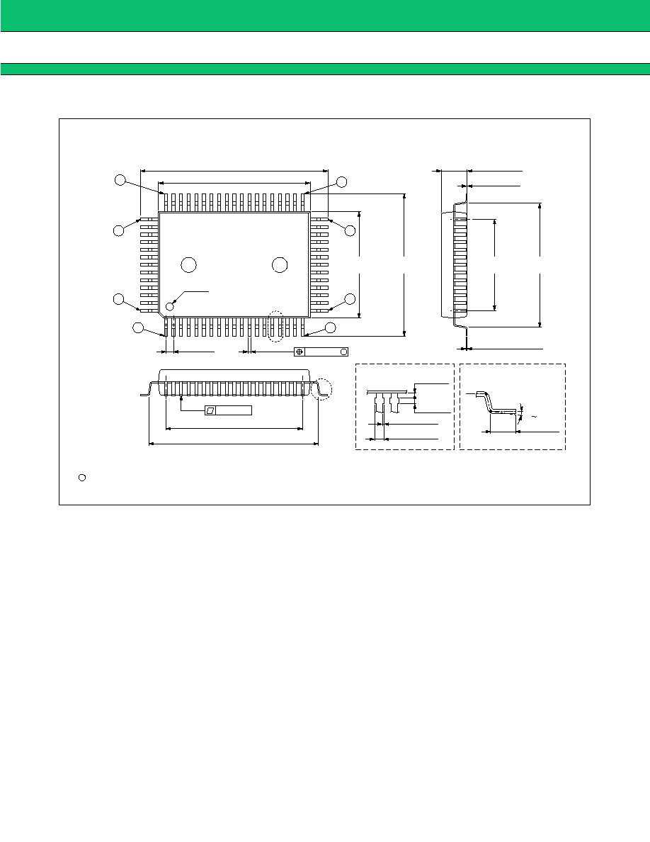
PACKAGES
(DIP-64P-M01)
64 pin, Plastic SH-DIP
(FPT-64P-M06)
64 pin, Plastic QFP

2
MB90091A
s
FEATURES
· Screen display capacity
: Up to 24 characters x 12 lines (288 characters)
· Font size
: 24 x 32 dots (horizontal x vertical)
· Font types
: 512 different characters (character codes 000H to 1FFH)
8 different sprite characters (character codes 1F8H to 1FFH)
(Internal or external ROM selectable)
· Display modes
: Trimmed display (pattern background 0, 1, or none)
Character background (settable for each character)
Shaded background (settable for each character)
· Sprite character display
: Capable of displaying one character (selectable from among 8 types of char-
acters) on the screen
Sprite character colors : 8 colors
Sprite trimming colors
: 8 colors
Sprite display position
: Settable in 2-dot units on the screen
· Character sizes
: Normal, double width, double height, double width x double height, quadruple
width, quadruple width x double height
(Set for each line)
· Display colors
: Character color
: 16 colors (set for each character)
Trimmed background color
: 16 colors (set for each line)
Character background color : 16 colors (set for each character)
Screen background color
: 16 colors
· Display position control
: Horizontal display start position : Set in 8-dot units
Vertical display start position
: Set in 2-dot units
Line spacing control
: Set in 2-dot units (0 to 30 dots)
· Character/color signal output : ROUT, GOUT, BOUT, IOUT (color signals)
COLOR (color/monochrome control signal)
VOB1 (character + pattern background + character background + screen
background: all-output signal)
VOB2 (character + pattern background + character background: specified-
character output signal)
· Supported TV systems
: NTSC, PAL, double-scan NTSC, double-scan PAL, 1250HDTV, 1125HDTV,
etc.
Personal computer monitor display systems such as VGA
· Intelligent features
: Automatic control of operation using on command table ROM
Command table ROM: Internal 32K bytes + external 32K bytes available
· Microcontroller/microcomputer interface : 8-bit serial input (3 signal input pins
Chip select: SCS
Serial clock: SCLK
Serial data: SIN
· Package
: SH-DIP-64, QFP-64
· Miscellaneous
: Power-on reset circuit integrated
3
MB90091A
s
PIN ASSIGNMENTS
(Continued)
1
COLOR
VOB2
64
2
DOCK
VOB1
63
3
V
SS
IOUT
62
4
TESTCK
BOUT
61
5
TESTSW
GOUT
60
6
HBLNK
ROUT
59
7
VBLNK
TRE
58
8
HSYNC
V
CC
57
9
VSYNC
SCS
56
10
EVEN
SIN
55
11
FLTIN
SCLK
54
12
AV
SS
FSEL
53
13
FLTOUT
TSEL
52
14
AV
CC
RA15
51
15
FH
RA14
50
16
RESET
RA13
49
17
V
CC
RA12
48
18
RD0
V
SS
47
19
RD1
RA11
46
20
RD2
RA10
45
21
RD3
RA9
44
22
RD4
RA8
43
23
RD5
RA7
42
24
RD6
RA6
41
25
RD7
RA5
40
26
TEST
V
SS
39
27
V
SS
RA4
38
28
TA16
V
CC
37
29
TA17
RA3
36
30
TA18
RA2
35
31
FCS
RA1
34
32
TCS
RA0
33
(SH-DIP-64P)
(TOP VIEW)
4
MB90091A
(Continued)
1
HSYNC
TRE
51
2
VSYNC
V
CC
50
3
EVEN
SCS
49
4
FLTIN
SIN
48
5
AV
SS
SCLK
47
6
FLTOUT
FSEL
46
7
AV
CC
TSEL
45
8
FH
RA15
44
9
RESET
RA14
43
10
V
CC
RA13
42
11
RD0
RA12
41
12
RD1
V
SS
40
13
RD2
RA11
39
14
RD3
RA10
38
15
RD4
RA9
37
16
RD5
RA8
36
17
RD6
RA7
35
18
RD7
RA6
34
19
TEST
RA5
33
(FPT-64P-M06)
(TOP VIEW)
VBLNK
64
HBLNK
63
TESTSW
62
TESTCK
61
V
SS
60
DOCK
59
COLOR
58
VOB2
57
VOB1
56
IOUT
55
BOUT
54
GOUT
53
ROUT
52
20
V
SS
21
TA16
22
TA17
23
TA18
24
FCS
25
TCS
26
RA0
27
RA1
28
RA2
29
RA3
30
V
CC
31
RA4
32
V
SS
5
MB90091A
s
PIN DESCRIPTION
(Continued)
Pin No.
Pin name
I/O
Function
DIP
QFP
8
1
HSYNC
I
Horizontal sync signal input pin
Dot clock generation is based on the cycle of the signal.
9
2
VSYNC
I
Vertical sync signal input pin
10
3
EVEN
I
Field control signal input pin
Input of an "L" level signal to this pin causes the font ROM address
LSB pin (RA0) to output an "L" level signal.
Input of an "H" level signal to this pin causes the font ROM address
LSB pin (RA0) to output an "H" level signal (when normal-size
characters are displayed).
This pin is disabled in noninterlaced mode.
11
4
FLTIN
O
Output pin for horizontal-sync phase comparison result signal
This pin is connected to an external lowpass filter.
13
6
FLTOUT
I
Internal VCO voltage input pin
This pin inputs the voltage signal from the external lowpass filter.
15
8
FH
O
Output pin for AFC-generated horizontal sync signal
16
9
RESET
I
Reset pin
This pin is enabled after release from a power-on reset.
18
19
20
21
22
23
24
25
11
12
13
14
15
16
17
18
RD0
RD1
RD2
RD3
RD4
RD5
RD6
RD7
I
External ROM data input pin
This pin inputs data from external font ROM or external command
data ROM.
26
19
TEST
I
Test signal input pin
This pin inputs an "L" level (fixed) signal during normal operation.
28
29
30
21
22
23
TA16
TA17
TA18
O
Test signal output pin
31
24
FCS
O
External font ROM chip select pin
32
25
TCS
O
Chip select pin for external command table ROM
6
MB90091A
(Continued)
(Continued)
Pin No.
Pin name
I/O
Function
DIP
QFP
33
34
35
36
38
40
41
42
43
44
45
46
48
49
50
51
26
27
28
29
31
33
34
35
36
37
38
39
41
42
43
44
RA0
RA1
RA2
RA3
RA4
RA5
RA6
RA7
RA8
RA9
RA10
RA11
RA12
RA13
RA14
RA15
O
External ROM address signal output pin
This pin outputs the signal specifying the external font ROM or
external command table ROM address.
External font ROM addresses
RA0 to RA4
: Raster addresses
RA5 to RA11 : Character codes (M0 to M6)
RA12, RA13 : Character horizontal address
= (0, 0): Left byte
= (1, 0): Center byte
= (0, 1): Right byte
RA14, RA15 : Character codes (M7, M8)
52
45
TSEL
I
Address control input pin for command table ROM
"L" level input : 0000H to 7FFFH Internal ROM
8000H to FFFFH External ROM
"H" level input : 0000H to 7FFFH External ROM
8000H to FFFFH Internal ROM
53
46
FSEL
I
Internal/external font ROM select pin
"L" level input : Select internal ROM.
"H" level input : Select external ROM.
54
47
SCLK
I
Shift clock input pin for serial transfer
55
48
SIN
I
Serial data input pin
56
49
SCS
I
Chip select pin
For serial transfer, set this pin to the "L" level.
This pin is also used to cancel a power-on reset.
58
51
TRE
O
Output pin for the signal indicating internal operation
This pin outputs an "H" level signal during data transfer from
command table ROM.
59
60
61
62
52
53
54
55
ROUT
GOUT
BOUT
IOUT
O
Chrominance signal output pin
For output of a character, character background, pattern background,
shaded background, screen background, or sprite character
(including a pattern background), this pin outputs the chrominance
signal.
63
56
VOB1
O
Pin for specifying the chrominance signal output period
This pin outputs an "H" level signal for output of a character, character
background, pattern background, shaded background, screen
background, or sprite character (including a pattern background.
64
57
VOB2
O
Pin for specifying the specified character output period
When the command 6: ATH bit = "1", this pin outputs an "H" level
signal in the character output period (24 x 32 dot period) when the
command 1: AT bit = "1".
The pin can be used for display control by an external circuit, for
example, for halftone display control.
7
MB90091A
(Continued)
Pin No.
Pin name
I/O
Function
DIP
QFP
1
58
COLOR
O
Color/monochrome select signal output pin
This pin allows "H" or "L" level output in each of the character,
character background, line background, screen background, and
sprite output periods to be specified depending on the internal
register setting.
Color/monochrome display is controlled by an external circuit.
(The following correspondence is used for convenience:
"L" level: Monochrome display
"H" level: Color display)
2
59
DOCK
O
Dot clock output pin
This pin outputs a dot clock signal when the command 11:DOT = "1".
4
61
TESTCK
I
Test signal input pin
This pin inputs an "H" level (fixed) signal during normal operation.
5
62
TESTSW
I
Test signal input pin
This pin inputs an "H" level (fixed) signal during normal operation.
6
63
HBLNK
I
Horizontal blanking signal input pin
This pin stops display signal output ("L" level output) when it inputs an
"L" level signal.
7
64
VBLNK
I
Vertical blanking signal input pin
This pin stops display signal output ("L" level output) when it inputs an
"L" level signal.
17
37
57
10
30
50
V
CC
--
+5 V power supply pin
27
39
47
3
20
32
40
60
V
SS
--
Ground pin
14
7
AV
CC
--
+5V power supply pin for VCO
12
5
AV
SS
--
Ground pin for VCO
8
MB90091A
s
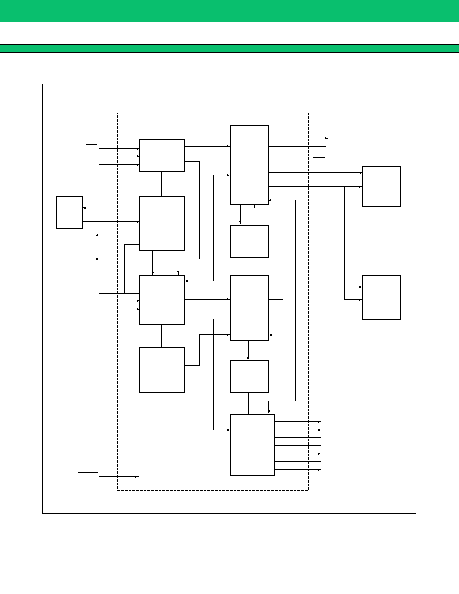
BLOCK DIAGRAM
RA0 to 15
RD0 to 7
TCS
FCS
DOCK
FH
LPF
FLTOUT
FLTIN
RESET
Resets each block.
MB90091A
Display data
output control
Dot clock
generator
SCS
SIN
SCLK
Command
table ROM
control
Command
table ROM
Command
table ROM
Font ROM
control
Font ROM
Font ROM
Display
memory
control
Display
memory
(VRAM)
HSYNC
VSYNC
EVEN
BOUT
ROUT
GOUT
IOUT
VOB 1
VOB 2
COLOR
FSEL
TRE
TSEL
Serial input
control
9
MB90091A
s
ABSOLUTE MAXIMUM RATINGS
(V
SS
= AV
SS
= 0 V)
*1: AV
CC
and V
CC
must have equal potential.
*2: Neither V
IN
nor V
OUT
must exceed "V
CC
+ 0.3 V".
WARNING: Semiconductor devices can be permanently damaged by application of stress (voltage, current,
temperature, etc.) in excess of absolute maximum ratings. Do not exceed these ratings.
s
RECOMMENDED OPERATING CONDITIONS
(V
SS
= AV
SS
= 0 V)
* : AV
CC
and V
CC
must have equal potential.
WARNING: Recommended operating conditions are normal operating ranges for the semiconductor device. All
the device's electrical characteristics are warranted when operated within these ranges.
Always use semiconductor devices within the recommended operating conditions. Operation outside
these ranges may adversely affect reliability and could result in device failure.
No warranty is made with repect to uses, operating conditions, or combinations not represented on
the data sheet. Users considering application outside the listed conditions are advised to contact their
FUJITSU representative beforehand.
Parameter
Symbol
Ratings
Unit
Min.
Max.
Power supply voltage *
1
V
CC
V
SS
0.3
V
SS
+
7.0
V
AV
CC
V
SS
0.3
V
SS
+
7.0
V
Input voltage *
2
V
IN
V
SS
0.3
V
SS
+
7.0
V
Output voltage *
3
V
OUT
V
SS
0.3
V
SS
+
7.0
V
Power consumption
Pd
--
500
mW
Operating temperature
Ta
0
+
70
°
C
Storage temperature
Tstg
55
+
150
°
C
Parameter
Symbol
Values
Unit
Remarks
Min.
Max.
Power supply voltage *
V
CC
4.75
5.25
V
Specification guarantee range
AV
CC
4.75
5.25
V
"H" level input voltage
V
IHS1
2.4
V
CC
+
0.3
V
RD0 to RD7 inputs
V
IHS2
0.8
×
V
CC
V
CC
+
0.3
V
Other inputs
"L" level input voltage
V
ILS1
0.3
0.45
V
RD0 to RD7 inputs
V
ILS2
V
SS
0.3
0.2
×
V
CC
V
Other inputs
Operating temperature
Ta
0
+
70
°
C
Analog input voltage
V
IN
0
V
CC
V
FLTOUT input
10
MB90091A
s
ELECTRICAL CHARACTERISTICS
1. DC Characteristics
Parameter
Symbol
Pin
Conditions
Values
Unit
Min.
Typ.
Max.
"H" level output voltage
V
OH
All out-
put pins
V
CC
= 4.75 V
I
OH
= 2.0 mA
4.0
--
--
V
"L" level output voltage
V
OL
V
CC
= 4.75 V
I
OL
= 4.0 mA
--
--
0.4
V
Input current
I
IL
HSYNC
VSYNC
EVEN
RESET
RD0 to
RD7
TSEL
FSEL
SCLK
SIN
SCS
HBLNK
VBLNK
V
CC
= 5.25 V
I
IL
= 4.0 mA
--
--
50
mA
Supply current
I
CC
V
CC
AV
CC
V
CC
= AV
CC
= 5.25 V
DOCK = 42 MHz
No load
--
--
40
mA
11
MB90091A
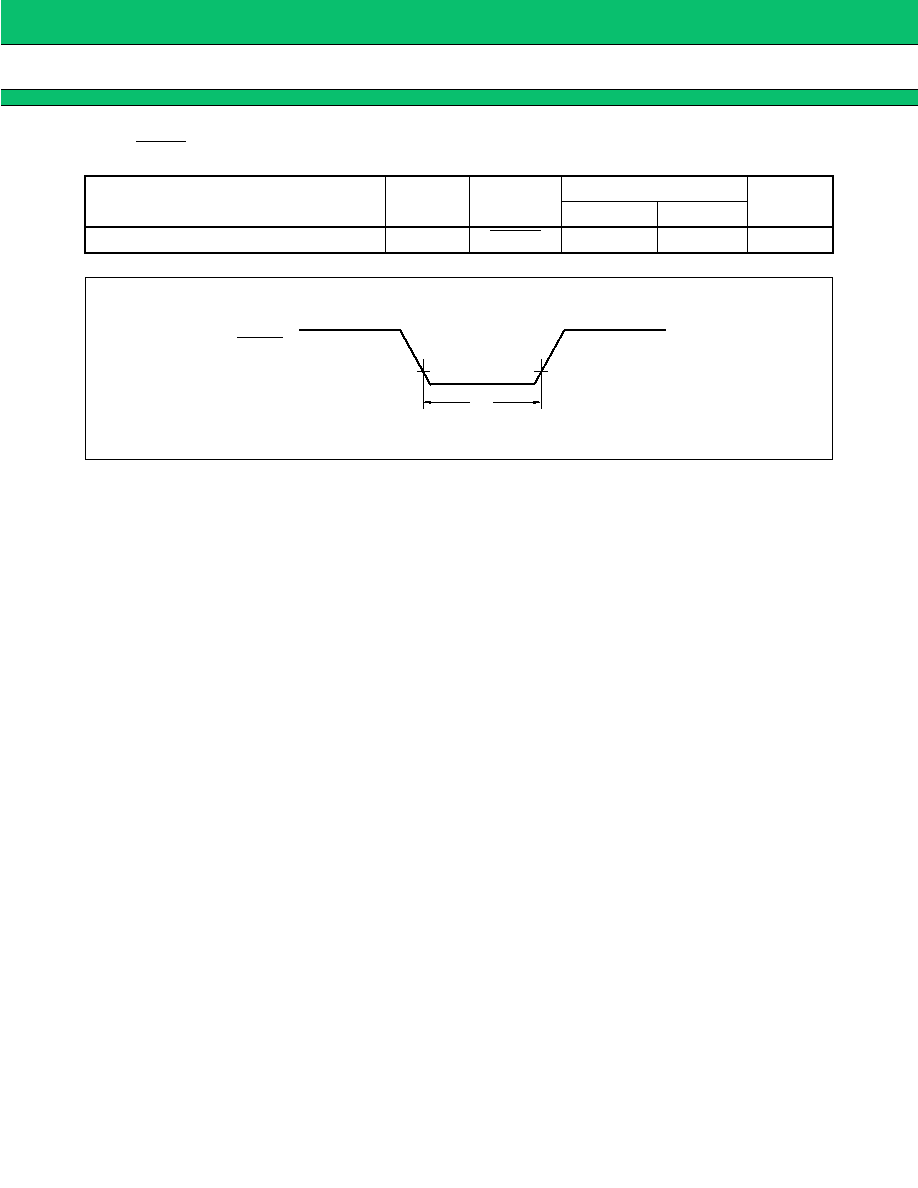
2. AC Characteristics
(1) Serial input timing
(V
CC
= AV
CC
= 5.0 V
±
5%, V
SS
= AV
SS
= 0 V, Ta = 0
°
C to +70
°
C)
Parameter
Symbol
Pin
Values
Unit
Min.
Max.
Shift clock cycle time
t
CVC
SCLK
1000
--
ns
Shift clock pulse width
t
WCH
SCLK
450
--
ns
t
WCL
450
--
ns
Shift clock signal rise/fall time
t
CR
SCLK
--
200
ns
t
CF
--
200
ns
Shift clock start time
t
SS
SCLK
200
--
ns
Data setup time
t
SU
SIN
200
--
ns
Data hold time
t
H
SIN
100
--
ns
Chip select end time
t
EC
SCS
500
--
ns
Chip select signal rise/fall time
t
CRC
SCS
--
200
ns
t
CFC
--
200
ns
0.8 V
CC
0.2 V
CC
t
CRC
0.8 V
CC
0.2 V
CC
t
SS
t
CFC
SCS
t
CYC
t
WCL
t
WCH
t
CR
t
CF
0.8 V
CC
0.2 V
CC
t
EC
SCLK
0.8 V
CC
0.2 V
CC
t
SU
t
H
SIN
12
MB90091A
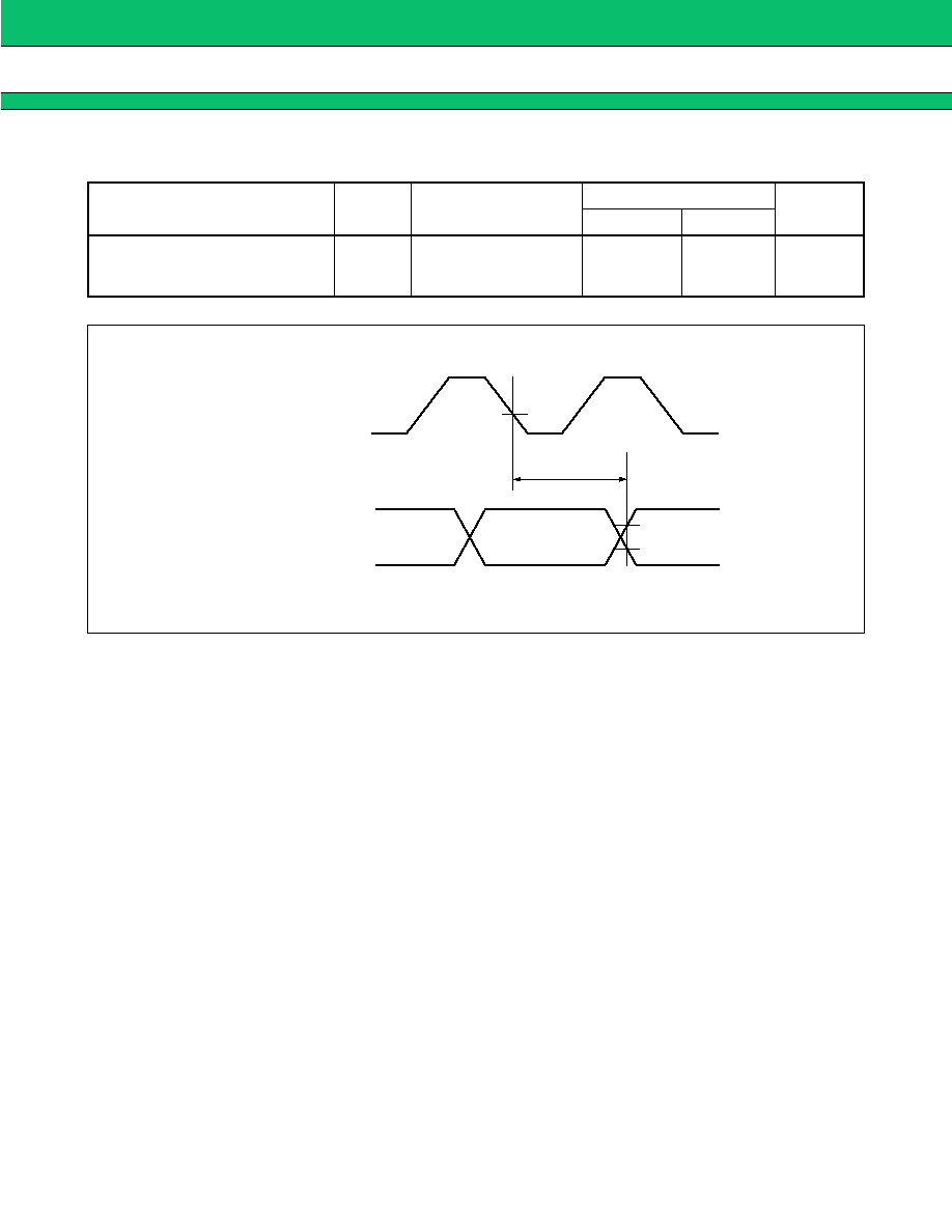
(2) Vertical and horizontal sync signal input timings
(V
CC
= AV
CC
= 5.0 V
±
5%, V
SS
= AV
SS
= 0 V, Ta = 0
°
C to +70
°
C)
Parameter
Symbol
Pin
Values
Unit
Min.
Max.
Horizontal sync signal rise time
t
HR
HSYNC
--
200
ns
Horizontal sync signal fall time
t
HF
HSYNC
--
200
ns
Vertical sync signal rise time
t
VR
VSYNC
--
200
ns
Vertical sync signal fall time
t
VF
VSYNC
--
200
ns
Horizontal sync signal pulse width
t
WH
HSYNC
1
--
µ
s
Vertical sync signal pulse width
t
WV
VSYNC
2
--
H
Horizontal sync signal setup time
t
HVST
VSYNC
5
--
µ
s
Vertical sync signal setup time
t
HVHD
VSYNC
5
--
µ
s
0.8 V
CC
0.2 V
CC
t
HR
0.8 V
CC
0.2 V
CC
HSYNC
t
WH
t
HF
0.8 V
CC
0.2 V
CC
t
VR
0.8 V
CC
0.2 V
CC
VSYNC
t
WV
t
VF
0.8 V
CC
t
HVST
0.8 V
CC
0.2 V
CC
t
HVHD
HSYNC
VSYNC
13
MB90091A
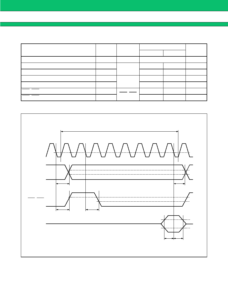
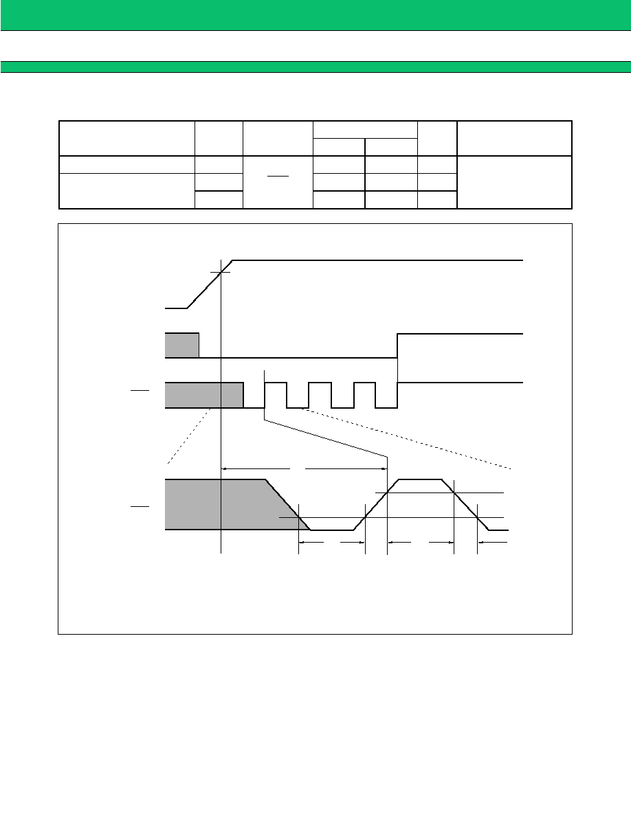
The MB90091A outputs display signals in synchronization with sync signals input from external circuits. The
signals required for controlling synchronization are the horizontal sync signal (input via the HSYNC pin), vertical
sync signal (input via the VSYNC pin), and field control signal (input via the EVEN pin).
The following examples illustrate external sync signal input timings applicable to general interlaced display.
Noninterlaced display does not require the EVEN pin signal.
Slow
*
2
Fast
*
2
FH
(HSYNC)
*
1
VSYNC
EVEN
FH
(HSYNC)
*
1
VSYNC
EVEN
· External sync signal input timing examples
(1) Field A
(2) Field B
*
2
*
2
*1: Input the horizontal sync signal to the HSYNC pin.
Input of a composite sync signal may change the FH signal cycle due to the PLL lock disturbed around
the VSYNC pulse, requiring a caution to be used for the timing of input to the EVEN pin. (See *2 below.)
*2: The input levels of the EVEN pin input signal in fields A and B are determined depending on the
relationship between the VSYNC and FH pulse positions. To the EVEN pin, input the "L" level signal in
the field in which the FH pulse after the rise of the VSYNC pulse appears fast. Pin the "H" level signal
in the field in which it appears slow.
The EVEN pin input signal should vary in the undisplay period such as around the VSYNC pulse.
14
MB90091A
(3) RESET signal input timing
(V
CC
= AV
CC
= 5.0 V
±
5%, V
SS
= AV
SS
= 0 V, Ta = 0
°
C to +70
°
C)
Parameter
Symbol
Pin
Values
Unit
Min.
Max.
Reset input pulse width
t
WR
RESET
10
--
µ
s
0.2 V
CC
0.2 V
CC
RESET
t
WR
15
MB90091A
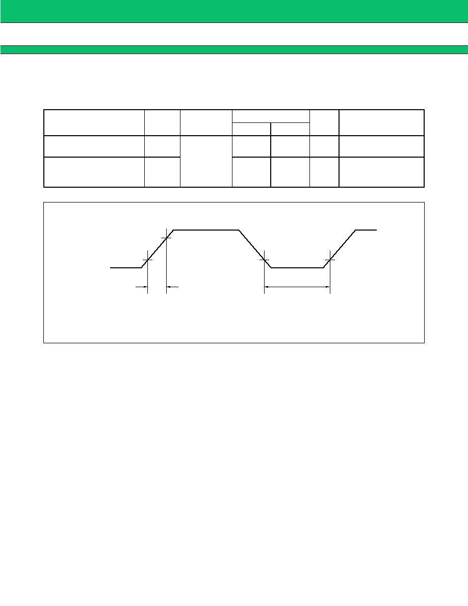
(4) Address data hold timing
(V
CC
= AV
CC
= 5.0 V
±
5%, V
SS
= AV
SS
= 0 V, Ta = 0
°
C to +70
°
C)
* : Dot clock = 84 to 42 MHz
Parameter
Symbol
Pin
Values
Unit
Min.
Max.
ROM read cycle
t
rcyc
--
Dot clock* x 8
--
Address valid delay
t
av
RA0 to
RA15
--
30
ns
Address invalid delay
t
ai
0
--
ns
Read data setup
t
ds
RD0 to RD7
30
--
ns
Read data hold
t
dh
0
--
ns
TCS, FCS active delay
t
ca
TCS, FCS
--
22
ns
TCS, FCS inactive delay
t
ci
0
--
ns
RA0 to 15
DOCK
TCS, FCS
RD0 to 7
t
rcyc
t
av
t
ai
t
ci
t
ca
t
ds
t
dh
0.2 V
CC
0.8 V
CC
0.2 V
CC
0.8 V
CC
0.2 V
CC
0.8 V
CC
0.2 V
CC
8
1
2
3
4
5
6
7
8
1
16
MB90091A
(5) Display data output timing
(V
CC
= AV
CC
= 5.0 V
±
5%, V
SS
= AV
SS
= 0 V, Ta = 0
°
C to +70
°
C)
Parameter
Symbol
Pin
Values
Unit
Min.
Max.
Display data output delay
t
d1
ROUT, GOUT, BOUT
IOUT, VOB1, VOB2
COLOR
0
22
ns
DOCK
0.8 V
CC
0.2 V
CC
ROUT, GOUT, BOUT
IOUT, VOB1, VOB2
COLOR
0.2 V
CC
t
d1
17
MB90091A
3. Power-on Reset Specifications
(1) Power ON-OFF timing
(Ta = 0
°
C to +70
°
C)
Parameter
Symbol
Pin
Values
Unit
Remarks
Min.
Max.
Power-supply rise time
t
r
V
CC
, AV
CC
0.05
50
ms
Power-on reset circuit
activating conditions
Power-supply shut-off time
t
off
1
--
ms
Conditions in which the
circuit repeatedly
operate normally
0.2 V
t
off
4.75 V
0.2 V
0.2 V
t
r
V
CC
Note: The power supply must be activated smoothly
18
MB90091A
(2) Power-on reset cancel timing
(Ta = 0
°
C to +70
°
C)
Parameter
Symbol
Pin
Values
Unit
Remarks
Min.
Max.
Time after rise
t
WIT
SCS
450
--
ns
Power-on reset cancel
timing
Reset cancel pulse width
t
WRH
450
--
ns
t
WRL
450
--
ns
0.8 V
CC
0.2 V
CC
4.75 V
V
CC
SCS
SCS
t
CRC
*
t
CFC
*
t
WRL
t
WRH
t
WIT
Internal reset
*: See the table in "(1) Serial timing" in Section 2 "AC Characteristics".
19
MB90091A
s
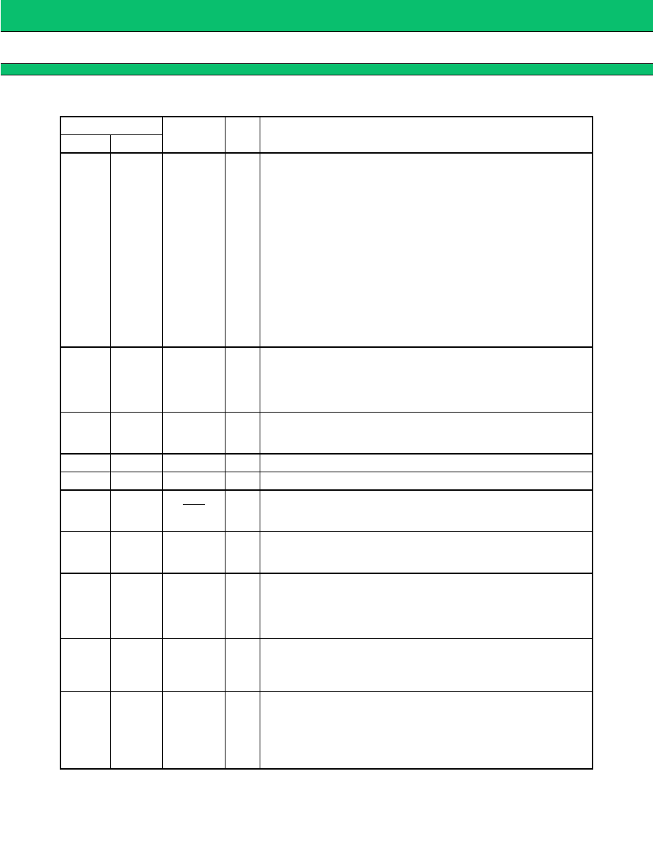
Command List
· List of display control commands
*1: The SA0 and EA0 bits can only be set to "0" and "1", respectively.
*2: Set the bits to "1".
Command
No.
First byte
Second byte
Function
Command code/data
Data
76543
2
1
0
7
6
5
4
3
2
1
0
0
10000
0
A8
A7
0
A6
A5
A4
A3
A2
A1
A0
Set write address
1
10001
AT
BS
B1
0
BG
BR
BB
CI
CG
CR
CB
Set character color
2
10010
0
M8
M7
0
M6
M5
M4
M3
M2
M1
M0
Set character code
3
10011
X9
X8
X7
0
0
G2
G1
G0
KGR KGD KGU Line control 1
4
10100
0
0
0
0
0
0
PC
PI
PG
PR
PB
Line control 2
5
10101 ATK ATR ATB
0
W3
W2
W1
W0
K24
P0
DC
Screen control 1
6
10110
SC
CC
BC
0
ATH
UC
UON
UI
UG
UR
UB
Screen control 2
7
10111
0
0
0
0
Y6
Y5
Y4
Y3
Y2
Y1
Y0
Set vertical display start
position
10111
1
0
0
0
X6
X5
X4
X3
X2
X1
X0
Set horizontal display start
position
8
11000 SP2 SP1 SP0
0
SCG SCR SCB SBP SBG SBR SBB Sprite control
9
11001
0
SY8 SY7
0
SY6 SY5 SY4 SY3 SY2 SY1
SY0
Set sprite vertical display
position
10
11010
0
SX8 SX7
0
SX6 SX5 SX4 SX3 SX2 SX1
SX0
Set sprite horizontal display
position
11
11011
0
DOT
0
0
1*
2
0
PR1 PR0
0
SC1
SC0 Synchronization control 1
11011
1
0
1*
2
0
DK6 DK5 DK4 DK3 DK2 DK1
DK0 Synchronization control 2
12
11100
0
0
SA7
0
SA6 SA5 SA4 SA3 SA2 SA1 SA0*
2
Set transfer start address 1
11100
1
0
SAF
0
SAE SAD SAC SAB SAA SA9
SA8 Set transfer start address 2
13
11101
0
0
EA7
0
EA6 EA5 EA4 EA3 EA2 EA1
EA0 Set transfer end address 1
11101
1
VBS EAF
0
EAE EAD EAC EAB EAA EA9
EA8 Set transfer end address 2
14
11110
--
--
--
--
--
--
--
--
--
--
--
(Reserved)
15
11111
--
--
--
--
--
--
--
--
--
--
--
(Reserved)
20
MB90091A
1. Command 0 (Set Write Address)
· Command format
· Function
Command 0 specifies the write address in display memory (VRAM). Before writing data using commands 1
and 2, use this command to determine the address to write that data at.
· Description
To set the VRAM address, specify the vertical column address (A8 to A5) and horizontal row address (A4 to
A0). The VRAM address is incremented automatically when a character code is set (by command 2).
A8 to A0: VRAM address
Set the VRAM address.
The A8 to A5 bits specify the vertical column address; the A4 to A0 bits specify the horizontal row address.
The row address is valid between 00H to 17H.
The column address is valid between 0H to BH.
Do not set the column or row address to any value outside the above valid range.
1
0
0
0
0
0
A8
A7
MSB
LSB
0
A1
A0
MSB
LSB
A6
A4
A5
A3
A2
A8 to A0: VRAM address
First byte
Second byte
21
MB90091A
2. Command 1 (Set Character Color)
· Command format
· Function
Command 1 sets the character color and character background color and specifies character qualification
display and shaded background display.
· Description
The character color, character background color, character qualification display, and shaded background dis-
play can be set/specified for each character. Character background display, blinking, and inverted shading
can be used for characters for which character qualification display is specified.
These settings are written to VRAM and applied to the display screen the moment command 2 (Set Character
Code) is issued.
AT: Specify character qualification display.
(Specify display of a character background, blinking, inverted shading.)
AT = 0: Normal display (without character qualification)
This setting suppresses character background display, blinking, and inverted shading in shaded
background display.
The output level at the VOB2 pin becomes "L".
AT = 1: Character qualification display
This setting enables character background display, blinking, and inverted shading in shaded back-
ground display.
"H" level output is enabled at the VOB2 pin.
Setting the command 5 (Screen Control 1) ATR bit to "1" specifies character background display.
Setting the ATB bit for command 5 (Screen Control 1) to "1" specifies blinking.
Setting both the ATK and BS bits for command 5 (Screen Control 1) to "1" specifies inverted
shading.
Setting the command 6 (Screen Control 2) ATH bit to "1" sets the output level at the VOB2 pin to "H".
BS: Specify shaded background display.
BS = 0: Normal display (without shaded background display)
BS = 1: Shaded background display
Setting both the ATK and AT bits for command 5 (Screen Control 1) to "1" specifies inverted
shading.
C1, CG, CR, CB: Set the character color.
B1, BG, BR, BB: Set the background color.
1
0
0
0
1
AT
BI
MSB
LSB
0
CR
CB
MSB
LSB
BG
BB
BR
CI
CG
BS
: Specify character qualification display.
(Specify display of a character background, blinking, inverted shading.)
: Specify shaded background display.
: Set a character background color.
: Set a character color.
First byte
Second byte
AT
BS
B1 to BB
C1 to CB
22
MB90091A
3. Command 2 (Set Character Code)
· Command format
· Function
Command 2 writes a character code to display memory (VRAM).
· Description
The character code data set by this command is written to display memory (VRAM) along with the character
color, character background color, shaded background display, and character qualification display data set by
command 1 (Set Character Color).
Character code is represented by nine bits from M8 to M0, enabling use of 512 different character patterns
from 000H to 1FFFH stored in internal or external font ROM.
Upon completion of writing data, the write address is incremented automatically.
M8 to M0: Character code
000H to 1FFFH can be set to specify 512 different characters.
1
0
0
1
0
0
M8
M7
MSB
LSB
0
M1
M0
MSB
LSB
M6
M4
M5
M3
M2
M8 to M0: Character code
First byte
Second byte
23
MB90091A
4. Command 3 (Line Control 1)
· Command format
· Function
Command 3 sets the line horizontal display start position, character size, and shaded background joint display
for each line.
· Description
Line control data set by this command is applied to the display screen when command 4 (Line Control 2) is
issued.
X9 to X7: Line horizontal display start position
The offset value can be set for each line, relative to the horizontal display start position set by
command 7-1 (Set Horizontal Display Start Position).
The valid range of values is 0 to 7H (In 2-character units: 0 to 14 characters)
First byte 1 0 0 1 1 X9 X7
MSB LSB
Second byte 0 KGD KGU
MSB LSB
0
G1
G2 G0 KGR
X8
X9 to X7
G2 to G0
KGR
KGD
KGU
: Line horizontal display start position
: Character size
: Specify shaded background left/right joint display
: Specify shaded background downward joint display
: Specify shaded background upward joint display
0
1
2
3
4
5
6
7
8
9
10
A
B
C
D
E
F
G
H
I
A
B
C
2 characters
8 characters
(X6 to X7)
(X9, X8, X7)
= (0, 0, 0)
= (0, 0, 1)
= (1, 0, 0)
· Line horizontal display start position
24
MB90091A
G2 to G0: Character size
Note: The horizontal display start position for "double width x single or double height" display is shifted three dots
to the right from that for normal-size display. The horizontal display start position for "quadruple width x single
or double height" display is shifted nine dots to the right from that for normal-size display. Be careful when
displaying normal-size and enlarged lines at the same time.
KGR: Specify shaded background left/right joint display.
KGR = 0: Display the shaded backgrounds horizontally adjacent to each other, joined together (without
display their adjacent, vertical sides).
KGR = 1: Display the shaded backgrounds horizontally adjacent to each other, separately for each character
(while displaying their adjacent, vertical sides).
KGD: Specify shaded background downward joint display.
KGD = 0: Display the shaded background including its lower side.
KGD = 1: Display the shaded background excluding its lower side.
KGU: Specify shaded background upward joint display
KGU = 0: Display the shaded background including its lower side.
KGU = 1: Display the shaded background excluding its lower side.
G2
G1
G0
Character size
0
0
0
Normal
0
0
1
Single height x double width
0
1
0
Double height x single width
0
1
1
Double height x double width
1
0
0
Single height x quadruple width
1
0
1
(Setting prohibited)
1
1
0
Double height x quadruple width
1
1
1
(Setting prohibited)

25
MB90091A
5. Command 4 (Line Control 2)
· Command format
· Function
Command 4 sets the pattern background color and controls it between color and monochrome modes.
· Description
The data set by this command is written to the column RAM specified by the VRAM column address set by
command 0 (Set Write Address), along with the line control data set by command 3 (Line Control 1).
The Line Control 1 and 2 data is applied to the display screen and the column address is incremented the
moment this command is issued.
PC: Control the pattern background color.
PC = 0: Display the pattern background in monochrome.
During the pattern background color output period, the COLOR pin remains at the "L" output level.
PC = 1: Display the pattern background in color.
During the pattern background color output period, the COLOR pin remains at the "H" output level.
PI, PG, PR, PG: Set the pattern background color.
First byte
1
0
1
0
0
0
0
0
MSB
LSB
Second byte
0
PR
PB
MSB
LSB
0
PC
0
PI
PG
PC
PI to PB
: Control the pattern background color.
: Set the pattern background color.
26
MB90091A
6. Command 5 (Screen Control 1)
· - Command format
· Function
Command 5 controls the display screen.
· Description
ATK: Control inverted shading.
ATK = 0: Normal display
Inverted display is disabled.
ATK = 1: Enable inverted display.
This mode displays those characters in reverse video (with the inverted, shaded background)
for which the BS and AT bits for command 1 (Set Character Color) have been both set to "1".
ATR: Control character background display.
ATR = 0: Normal display
Character background display is disabled.
ATR = 1: Enable character background display.
Character background display applies to those characters for which the BS and AT bits for
command 1 (Set Character Color) have been set to "0" and "1", respectively.
ATB: Control blinking.
ATB = 0: Normal display
Blinking is disabled.
ATB = 1: Enable blinking.
This mode causes those characters to blink for which the AT bit for command 1 (Set Character
Color) has been set to "1".
W3 to W0: Control the line spacing.
Set the line spacing in 2-dot units.
0 to 30 dots can be specified.
First byte
1
0
1
0
1
ATK
ATB
MSB
LSB
Second byte
0
P0
DC
MSB
LSB
W3
W1
W2
W0
K24
ATR
ATK
ATR
ATB
W3 to W0
K24
P0
DC
: Control inverted shading.
: Control character background display.
: Control blinking.
: Control the line spacing.
: Specify the shadow frame szize.
: Control the pattern background.
: Control displ

27
MB90091A
K24: Specify the shadow frame size.
K24 = 0: Set the height of shadow frames for shaded background display to 32 dots.
K24 = 1: Set the height of shadow frames for shaded background display to 24 dots.
P0: Control the pattern background.
P0 = 0: Set pattern background mode "pattern background 0".
ROM data "1" is displayed as a character dot.
P0 = 1: Set pattern background mode "pattern background 1".
Character and pattern background dots are separately generated automatically from a ROM
data array.
Note: Note: As the pattern background mode, set the mode used when the relevant font was designed.
DC: Control display.
DC = 0: Disable output operation for displaying characters and sprite characters.
Only the screen background color can be output.
DC = 0: Enable output operation for displaying characters and sprite characters.
The screen background color can also be output.
28
MB90091A
7. Command 6 (Screen Control 2)
· Command format
· Function
Command 6 specifies the character color, character background color, screen background color, sprite char-
acter color, color/monochrome mode, specified character output. This command also enables or disables
screen background color output and sets the screen background color.
· Description
SC: Control the sprite character color.
SC = 0: Display the sprite character and sprite pattern background in monochrome.
During the sprite character/pattern background output period, the COLOR pin outputs the "L"
level signal.
SC = 1: Display the sprite character and sprite pattern background in color.
During the sprite character/pattern background output period, the COLOR pin outputs the "H"
level signal.
CC: Control the character color.
CC = 0: Display characters in monochrome.
During the character output period, the COLOR pin outputs the "L" level signal.
CC = 1: Display characters in color.
During the character output period, the COLOR pin outputs the "H" level signal.
BC: Control the character background.
BC = 0: Display the character background in monochrome.
During the character background output period, the COLOR pin outputs the "L" level signal.
BC = 1: Display the character background in color.
During the character background output period, the COLOR pin outputs the "H" level signal.
Note: Note: Use an external circuit to control display mode between monochrome and color using the COLOR pin.
First byte
1
0
1
1
0
SC
BC
MSB
LSB
Second byte
0
UR
UB
MSB
LSB
ATH
UON
UC
UI
UG
CC
SC
CC
BC
ATH
UC
UON
UI to UB
: Control the sprite character color.
: Control the character color.
: Control the character background.
: Control specified character output.
: Control the screen background color.
: Control screen beckground color output.
: Set the screen background color.

29
MB90091A
ATH: Control specified character output.
ATH = 0: Normal display
The VOB2 pin outputs the "L" level signal.
ATH = 1: The VOB2 pin outputs the "H" level signal during the output period (24 x 32b dots period) for
those characters for which the AT bit for command 1 (Set Character Color) has been set to 1.
Note: Note: Use an external circuit to handle the VOB2 pin signal, allowing the specified character to be displayed
in halfbright, translucent, and other special display mode.
UC: Control the screen background color.
UC = 0: Display the screen background in monochrome.
During the screen background output period, the COLOR pin outputs the "L" level signal.
UC = 1: Display the screen background in color.
During the screen background output period, the COLOR pin outputs the "H" level signal.
UON: Control screen background color output.
UON = 0: Prevent the screen background color from being output.
During the screen background color output period, the IOUT, GOUT, ROUT, BOUT, and VOB1
pins output "L" level signals.
UON = 1: Output the screen background color.
During the screen background color output period, the IOUT, GOUT, ROUT, and BOUT pins
output the screen background color and the VOB1 pin outputs the "L" level signal.
UI, UG, UR, UB: Set the screen background color.
30
MB90091A
8. Command 7-0 (Set Vertical Display Start Position)
· Command format
· Function
Command 7-0 sets the vertical display start position.
· Description
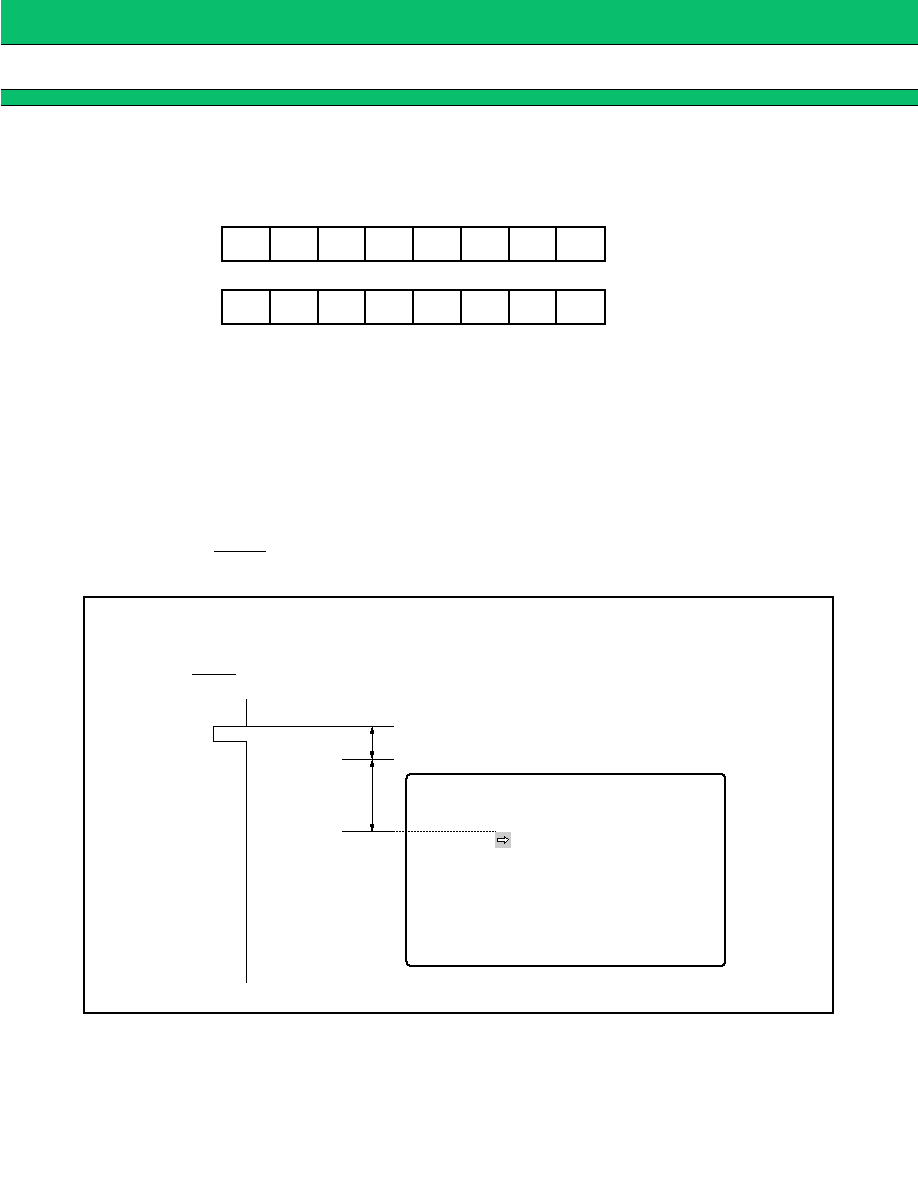
Y6 to Y0: Set the vertical display start position.
Set the position to start vertical display. The valid range of values is 00H to 7FH for setting in 2-dot
units (0 to 254 dots).
The following illustrates the relationship between the vertical display start position and the *VSYNC
signal.
· Vertical display start position
First byte
1
0
1
1
1
0
0
MSB
LSB
Second byte
0
Y1
Y0
MSB
LSB
Y6
Y4
Y5
Y3
Y2
0
Y6 to Y0: Set the vertical display start position.
VSYNC
20H
Vertical display
start position
31
MB90091A
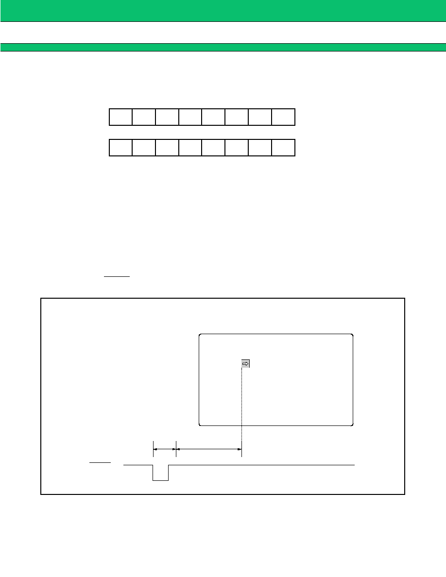
9. Command 7-1 (Set Horizontal Display Start Position)
· Command format
· Function
Command 7-0 sets the horizontal display start position.
· Description
X6 to X0: Set the horizontal display start position.
Set the position to start horizontal display. The valid range of values is 00H to 7FH for setting in 8-
dot units.
The following illustrates the relationship between the horizontal display start position and the YSYNC
signal.
· Horizontal display start position
* : Character size: About 100-dot clock for normal display
Double or quadruple width display is shifted further to the right from the above value.
For details, see Page 24
First byte
1
0
1
1
1
1
0
MSB
LSB
Second byte
0
X1
X0
MSB
LSB
X6
X4
X5
X3
X2
0
X6 to X0: Set the horizontal display start position.
Horizontal operation
started*
Horizontal display start position
HSYNC
32
MB90091A
10.Command 8 (Sprite Control)
· Command format
· Function
Command 8 sets the sprite character code, character color, pattern background display, and pattern back-
ground color.
· Description
SP2 to SP0: Set sprite character code.
Specify the sprite character type from among character codes 1F8H to 1FFH representing eight
character types.
SCG to SCB: Set the sprite character color.
SBP: Control sprite pattern background display.
SBP = 0: Display no pattern background for the sprite.
This display mode is "No pattern background" (displaying only those character dots displayed
in "Pattern background 1" mode).
SBP = 1: Display a pattern background for the sprite.
This display mode is "Pattern background 1".
SBG to SBB: Set the sprite pattern background color.
SP2
SP1
SP0
Sprite character
0
0
0
1F8
H
0
0
1
1F9
H
0
1
0
1FA
H
0
1
1
1FB
H
1
0
0
1FC
H
1
0
1
1FD
H
1
1
0
1FE
H
1
1
1
1FF
H
First byte
1
1
0
0
0
SP2
SP0
MSB
LSB
Second byte
0
SBR
SBB
MSB
LSB
SCG
SCB
SCR
SBP
SBG
SP1
SP2 to SP0
SCG to SCB
SBP
SBG to SBB
: Set sprite character code.
: Set the sprite character color.
: Set the sprite pattern background.
: Set the sprite pattern background color.
33
MB90091A
11.Command 9 (Set Sprite Vertical Display Position)
· Command format
· Function
Command 9 sets the sprite character vertical display position.
· Description
SY8 to SY0: Set the sprite vertical display position.
Set the vertical display position of the sprite character.
The valid range of values is 000H to 1FFH for setting in 2-dot units (0 to 1022 dots).
The following illustrates the relationship between the sprite vertical display position and the
VSYNC signal.
First byte
1
1
0
0
1
0
SY7
MSB
LSB
Second byte
0
SY1
SY0
MSB
LSB
SY6
SY4
SY5
SY3
SY2
SY8
SY8 to SY0: Set the sprite vertical display position.
VSYNC
Sprite vertical
display position
20H
· Sprite vertical display position
34
MB90091A
12.Command 10 (Set Sprite Horizontal Display Position)
· Command format
· Function
Command 10 sets the sprite character horizontal display position.
· Description
SY8 to SY0: Set the sprite horizontal display position.
Set the horizontal display position of the sprite character.
The valid range of values is 000H to 1FFH for setting in 2-dot units (0 to 1022 dots).
Setting these bits to 000H disables sprint display.
The following illustrates the relationship between the sprite horizontal display position and the
HSYNC signal.
* : About 80-dot clock.
First byte
1
1
0
1
0
0
SX7
MSB
LSB
Second byte
0
SX1
SX0
MSB
LSB
SX6
SX4
SX5
SX3
SX2
SX8
SX8 to SX0: Set the sprite horizontal display position.
Sprite horizontal display started*
Sprite horizontal display position
HSYNC
· Sprite horizontal display position
35
MB90091A
13.Command 11-0 (Synchronization Control 1)
· Command format
· Function
Command 10 controls synchronization.
· Description
DOT: Control dot clock output.
DOT = 0: Do not output the dot clock signal to the DOCK pin.
DOT = 1: Output the dot clock signal to the dock pin.
PR1, PR0: Control the prescaler.
SC1, SC0: Control the scan system.
Interlaced or step scan operation requires the field control signal to be input to the EVEN pin.
PR1
PR0
Prescaler operation
Corresponding dot clock
0
0
÷
2
25.0 to 42.0 MHz
0
1
÷
3
16.7 to 28.3 MHz
1
0
÷
5
10.0 to 17.0 MHz
1
1
÷
6
8.4 to 14.1 MHz
SC1
SC2
Scan system
0
0
Interlaced scan
0
1
Noninterlaced scan
1
0
Step scan
1
1
(Setting prohibited)
First byte
1
1
0
1
1
0
0
MSB
LSB
Second byte
0
SC1
SC0
MSB
LSB
1*
PR1
0
PR0
0
DOT
DOT
PR1, PR0
SC1, SC0
*: Set this bit to "1".
: Control dot clock output.
: Control the prescaler.
: Control the scan system.
36
MB90091A
14.Command 11-1 (Synchronization control 2)
· Command format
· Function
Command 11-1 controls dot clock signals.
· Description
DK6 to DK0: Control dot clock signals.
Set the divisor in 16-dot units for generating dot clock signals by dividing the FH (horizontal
frequency). The valid range of values is 00H to 7FH.
This enables the horizontal frequency to be divided by up to 2032.
15.Command 12-0 (Set Transfer Start Address 1)
· Command format
· Function
Command 12-0 sets the lower address for starting transfer of data from command table ROM.
· Description
SA7 to SA0: Lower address for starting transfer from command table ROM
These bits can be set only to an even address. The SA0 bit is set internally to "0".
Data transfer from ROM is initiated by issuing command 13-1 (Set Transfer End Address 2).
First byte
1
1
0
1
1
1
1*
MSB
LSB
Second byte
0
DK1
DK0
MSB
LSB
DK6
DK4
DK5
DK3
DK2
0
DK6 to DK0: Control dot clock signals.
*: Set this bit to "1".
First byte
1
1
1
0
0
0
SA7
MSB
LSB
Second byte
0
SA1
SA0*
MSB
LSB
SA6
SA4
SA5
SA3
SA2
0
SA7 to SA0: Lower address for starting transfer from command table ROM
*: The SA0 bit can only be set to "0".

37
MB90091A
16.Command 12-1 (Set Transfer Start Address 2)
· Command format
· Function
Command 12-1 sets the upper address for starting transfer of data from command table ROM.
· Description
SAF to SA8: Upper address for starting transfer from command table ROM
Data transfer from ROM is initiated by issuing command 13-1 (Set Transfer End Address 2).
17.Command 13-0 (Set Transfer End Address 1)
· Command format
· Function
Command 13-0 sets the lower address for ending transfer of data from command table ROM.
· Description
EA7 to EA0: Lower address for ending transfer from command table ROM
These bits can be set only to an odd address. The EA0 bit is set internally to "1".
Data transfer from ROM is initiated by issuing command 13-1 (Set Transfer End Address 2).
First byte
1
1
1
0
0
1
SAF
MSB
LSB
Second byte
0
SA9
SA8
MSB
LSB
SAE
SAC
SAD
SAB
SAA
0
SAF to SA8: Upper address for starting transfer from command table ROM
First byte
1
1
1
0
1
0
EA7
MSB
LSB
Second byte
0
EA1
EA0*
MSB
LSB
EA6
EA4
EA5
EA3
EA2
0
EA7 to SA0: Lower address for ending transfer from command table ROM
*: The EA0 bit can onlybe set to "1".

38
MB90091A
18.Command 13-1 (Set Transfer End Address 2)
· Command format
· Function
Command 13-1 sets the upper address for ending data transfer from command table ROM and specifies the
ROM transfer period to initiate ROM data transfer.
· Description
VBS: Control the ROM transfer period.
VBS = 0: Transfer data during the horizontal and vertical blanking intervals.
VBS = 1: Transfer data during the vertical blanking interval.
EAF to EA8: Upper address for ending transfer from command table ROM
Issuing this command initiates command table ROM transfer operation and sets the TRE pin output to the "H"
level. Upon completion of transfer operation, the TRE pin output becomes the "L" level.
When the TRE pin output is at the "H" level, do not issue command 0 to 4, 11, 12, or 13 by serial input
(commands 5 to 10 can be issued).
First byte
1
1
1
0
1
1
EAF
MSB
LSB
Second byte
0
EA9
EA8
MSB
LSB
EAE
EAC
EAD
EAB
EAA
VBS
VBS
EAF to EA8
: Control the ROM transfer period.
: Upper address for ending transfer from command table ROM
39
MB90091A
s
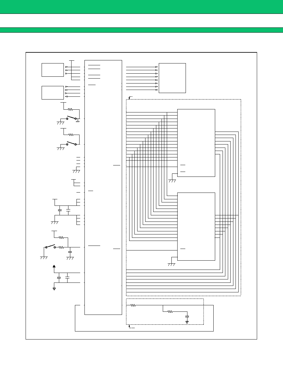
APPLICATION EXAMPLES
This section provides useful information for designing application systems using the MB90091A.
1. Power Supply
The MB90091A pairs of digital (V
CC
, V
SS
) and analog (AV
CC
, AV
SS
) power-supply and ground pins. The V
CC
and
AV
CC
power-supply pins are independent of each other; the V
SS
and AV
SS
ground pins are internally common.
Since the analog power supply supplies power and control voltage to the internal VCO, it requires special
consideration separately from the digital power supply.
In general, pay attention to the following points:
· Design the system so that the ground and power supply impedances are suppressed. In addition, the ground
line should be laid out on a ground plane including peripheral analog circuits.
· The digital (V
CC
, V
SS
) and analog (AV
CC
, AV
SS
) power supplies must be separated from each other. The V
CC
and AV
CC
pins, and the V
SS
and AV
SS
pins must not have a potential different in between.
· To supply digital and analog power from the same power source, separately route the wires from the source
and use a choke coil to prevent digital noise from interfering with the analog subsystem via the power source.
· Insert a relatively high-capacity (20 to 100
µ
F) electrolytic capacitor as a bypass capacitor between the power
supply and ground, separately between the digital and analog subsystems.
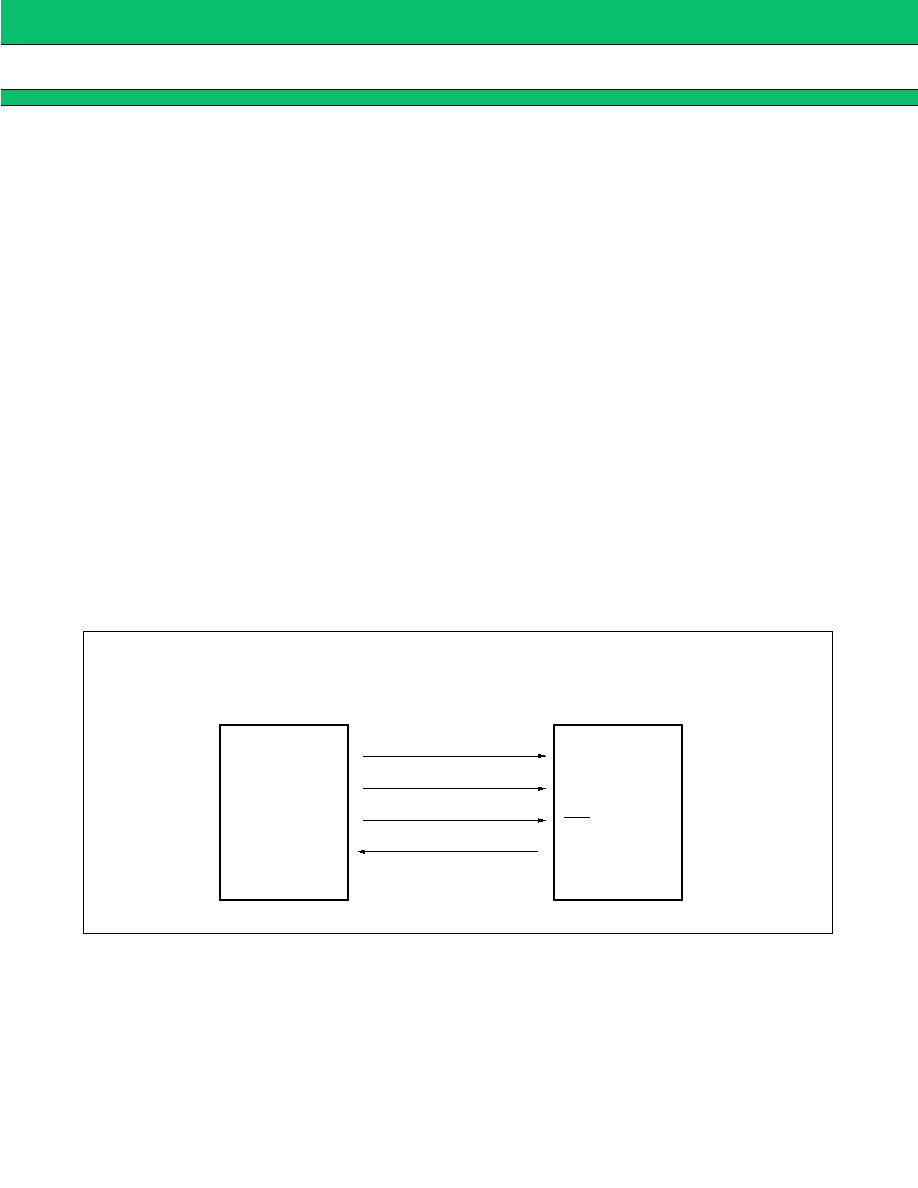
2. Interface with a Microcontroller or Microcomputer
Operation of the MB90091 is controlled by a micro (controller or microcomputer). The MB90091 interfaces with
the micro by 8-bit serial transfer using four signal liens as shown below:
Although most micros can be used for controlling the MB90091A, the one with an 8-bit serial interface (serial
port) is recommended because it can be connected directly to the MB90091A for high-speed command/data
transfer by means of hardware. (The micro with a 4-bit serial interface can transfer data in two separate blocks.)
Note: Keep in mind that some micros cannot be connected to the serial port depending on the type. Fujitsu 4- and
8-bit microcontrollers have no problem with the MB90091A.
Micro
MB90091A
Data
SO
TC
Port
Port
(or interrupt input)
SIN
SCLK
SCS
TRE
Serial clock
Chip select
Internal operation flag
· Microcontroller/microcomputer interface
40
MB90091A
3. Treatment of Unused Pins
Pins unused on the MB90091A must be treated as follows.
· Treatment of unused pins
(Continued)
Pin No.
Pin name
I/O
Treatment
DIP
QFP
8
1
HSYNC
I
--
9
2
VSYNC
I
--
10
3
EVEN
I
Connect the pin to V
CC
or leave it open.
11
4
FLTIN
O
--
13
6
FLTOUT
I
--
15
8
FH
O
Leave the pin open.
16
9
RESET
I
Connect the pin to V
CC
or leave it open.
18
19
20
21
22
23
24
25
11
12
13
14
15
16
17
18
RD0
RD1
RD2
RD3
RD4
RD5
RD6
RD7
I
I
I
I
I
I
I
I
Connect the pin to V
CC
or leave it open.
Connect the pin to V
CC
or leave it open.
Connect the pin to V
CC
or leave it open.
Connect the pin to V
CC
or leave it open.
Connect the pin to V
CC
or leave it open.
Connect the pin to V
CC
or leave it open.
Connect the pin to V
CC
or leave it open.
Connect the pin to V
CC
or leave it open.
26
19
TEST
I
Connect the pin to V
SS
.
28
29
30
21
22
23
TA16
TA17
TA18
O
O
O
Leave the pin open.
Leave the pin open.
Leave the pin open.
31
24
FCS
O
Leave the pin open.
32
25
TCS
O
Leave the pin open.
33
34
35
36
38
40
41
42
43
44
45
46
48
49
50
51
26
27
28
29
31
33
34
35
36
37
38
39
41
42
43
44
RA0
RA1
RA2
RA3
RA4
RA5
RA6
RA7
RA8
RA9
RA10
RA11
RA12
RA13
RA14
RA15
O
O
O
O
O
O
O
O
O
O
O
O
O
O
O
O
Leave the pin open.
Leave the pin open.
Leave the pin open.
Leave the pin open.
Leave the pin open.
Leave the pin open.
Leave the pin open.
Leave the pin open.
Leave the pin open.
Leave the pin open.
Leave the pin open.
Leave the pin open.
Leave the pin open.
Leave the pin open.
Leave the pin open.
Leave the pin open.
52
45
TSEL
I
--
53
46
FSEL
I
--
54
47
SCLK
I
--
55
48
SIN
I
--
41
MB90091A
(Continued)
Pin No.
Pin name
I/O
Treatment
DIP
QFP
56
49
SCS
I
--
58
51
TRE
O
Leave the pin open.
59
52
ROUT
O
Leave the pin open.
60
53
GOUT
O
Leave the pin open.
61
54
BOUT
O
Leave the pin open.
62
55
IOUT
O
Leave the pin open.
63
56
VOB1
O
Leave the pin open.
64
57
VOB2
O
Leave the pin open.
1
58
COLOR
O
Leave the pin open.
2
59
DOCK
O
Leave the pin open.
4
61
TESTCK
I
Connect the pin to V
CC
or leave it open.
5
62
TESTSW
I
Connect the pin to V
CC
.
6
63
HBLNK
I
Connect the pin to V
CC
or leave it open.
7
64
VBLNK
I
Connect the pin to V
CC
or leave it open.
42
MB90091A
s
APPLIED CIRCUIT EXAMPLE
+
-
+
-
+
-
+
-
Sync signal
separation
Micro
V
CC
MB90091A
HSYNC
VSYNC
EVEN
HBLNK
VBLNK
SCS
SIN
SCLK
TRE
FSEL
TSEL
TA16
TA17
TA18
TEST
TESTSW
TESTCK
FH
V
CC
V
CC
V
CC
V
SS
V
SS
V
SS
V
SS
RESET
AV
CC
AV
SS
FLTOUT
ROUT
GOUT
BOUT
IOUT
VOB1
COLOR
VOB2
DOCK
RA0
RA1
RA2
RA3
RA4
RA5
RA6
RA7
RA8
RA9
RA10
RA11
RA12
RA13
RA14
RA15
FCS
TCS
RD7
RD6
RD5
RD4
RD3
RD2
RD1
RD0
FLTIN
V
CC
V
CC
V
CC
V
CC
V
CC
AV
CC
AGND
10 K
GND
10 K
10 K
GND
NC
NC
NC
GND
NC
10
µ
0.1
µ
1
µ
GND
GND
GND
47
0.1
µ
10
µ
Display control
V
CC
GND
AV
CC
AGND
: +5 V (digital)
: Ground (digital)
: +5 V (analog)
: Grond (analog)
This circuit is not required when internal ROM is used.
(512-character font ROM)
64K-byte ROM
A0
A1
A2
A3
A4
A5
A6
A7
A8
A9
A10
A11
A12
A13
A14
A15
OE
CE
GND
(Command table ROM)
32K-byte ROM
A0
A1
A2
A3
A4
A5
A6
A7
A8
A9
A10
A11
A12
A13
A14
OE
CE
GND
O1
O2
O3
O4
O5
O6
O7
O8
O1
O2
O3
O4
O5
O6
O7
O8
330
51
AGND
1
µ
Adjustment is required depending on synchronization system.
1
2
3
63
64
49
48
47
51
46
45
21
22
23
19
62
61
8
10
30
50
20
32
40
60
9
7
5
6
4
18
17
16
15
14
13
12
11
25
24
26
27
28
29
31
33
34
35
36
37
38
39
41
42
43
44
52
53
54
55
56
58
57
59
43
MB90091A
s
ORDERING INFORMATION
Part number
Package
Remarks
MB90091AP
64-pin plastic SH-DIP
(DIP-64P-M01)
MB90091APF
64-pin plastic QFP
(FPT-64P-M06)
44
MB90091A
s
PACKAGE DIMENSIONS
(Continued)
(DIP-64P-M01)
64 pin, Plastic SH-DIP
+0.50
0
0
+.020
.022
+.008
0.55
+0.22
55.118(2.170)REF
INDEX-2
15°MAX
TYP
19.05(.750)
(.010±.002)
0.25±0.05
MAX
1.778(.070)
(.070±.007)
1.778±0.18
1.00
.039
(.018±.004)
0.45±0.10
0.51(.020)MIN
3.00(.118)MIN
5.65(.222)MAX
INDEX-1
(.669±.010)
17.00±0.25
2.283
58.00
1994 FUJITSU LIMITED D64001S-3C-4
C
Dimensions in mm (inches).
45
MB90091A
(FPT-64P-M06)
64 pin, Plastic QFP
"A"
LEAD No.
64
52
32
0.25(.010)
0.30(.012)
51
33
1
19
20
INDEX
TYP
(.016±.004)
0.40±0.10
1.00(.0394)
0.15±0.05(.006±.002)
18.00(.709)REF
22.30±0.40(.878±.016)
(STAND OFF)
0.05(.002)MIN
3.35(.132)MAX
(.551±.008)
14.00±0.20
(.642±.016)
16.30±0.40
REF
12.00(.472)
(.736±.016)
18.70±0.40
20.00±0.20(.787±.008)
24.70±0.40(.972±.016)
(.047±.008)
Details of "B" part
1.20±0.20
0 10°
Details of "A" part
0.18(.007)MAX
0.63(.025)MAX
0.10(.004)
"B"
M
0.20(.008)
1994 FUJITSU LIMITED F64013S-3C-2
C
(Mounting height)
Dimensions in mm (inches).

48
MB90091A
All Rights Reserved.
The contents of this document are subject to change without
notice. Customers are advised to consult with FUJITSU sales
representatives before ordering.
The information and circuit diagrams in this document presented
as examples of semiconductor device applications, and are not
intended to be incorporated in devices for actual use. Also,
FUJITSU is unable to assume responsibility for infringement of
any patent rights or other rights of third parties arising from the
use of this information or circuit diagrams.
FUJITSU semiconductor devices are intended for use in
standard applications (computers, office automation and other
office equipment, industrial, communications, and measurement
equipment, personal or household devices, etc.).
CAUTION:
Customers considering the use of our products in special
applications where failure or abnormal operation may directly
affect human lives or cause physical injury or property damage,
or where extremely high levels of reliability are demanded (such
as aerospace systems, atomic energy controls, sea floor
repeaters, vehicle operating controls, medical devices for life
support, etc.) are requested to consult with FUJITSU sales
representatives before such use. The company will not be
responsible for damages arising from such use without prior
approval.
Any semiconductor devices have inherently a certain rate of
failure. You must protect against injury, damage or loss from
such failures by incorporating safety design measures into your
facility and equipment such as redundancy, fire protection, and
prevention of over-current levels and other abnormal operating
conditions.
If any products described in this document represent goods or
technologies subject to certain restrictions on export under the
Foreign Exchange and Foreign Trade Control Law of Japan, the
prior authorization by Japanese government should be required
for export of those products from Japan.
FUJITSU LIMITED
For further information please contact:
Japan
FUJITSU LIMITED
Corporate Global Business Support Division
Electronic Devices
KAWASAKI PLANT, 4-1-1, Kamikodanaka
Nakahara-ku, Kawasaki-shi
Kanagawa 211-88, Japan
Tel: (044) 754-3753
Fax: (044) 754-3329
North and South America
FUJITSU MICROELECTRONICS, INC.
Semiconductor Division
3545 North First Street
San Jose, CA 95134-1804, U.S.A.
Tel: (408) 922-9000
Fax: (408) 432-9044/9045
Europe
FUJITSU MIKROELEKTRONIK GmbH
Am Siebenstein 6-10
63303 Dreieich-Buchschlag
Germany
Tel: (06103) 690-0
Fax: (06103) 690-122
Asia Pacific
FUJITSU MICROELECTRONICS ASIA PTE. LIMITED
#05-08, 151 Lorong Chuan
New Tech Park
Singapore 556741
Tel: (65) 281 0770
Fax: (65) 281 0220
F9704
©
FUJITSU LIMITED Printed in Japan
Document Outline