
Version 1.3
FUJITSU SEMICONDUCTOR
DATA SHEET
16-bit Proprietary Microcontroller
CMOS
F
2
MC-16LX MB90370 Series
MB90372/F372/V370
DESCRIPTION
The MB90370 series is a line of general-purpose, 16-bit microcontrollers designed for those applications which
require high-speed real-time processing. The instruction set is designed to be optimized for controller applications
which inheriting the AT architecture of F
2
MC-16LX series and allow a wide range of control tasks to be processed
efficiently at high speed.
A built-in LPC interface, serial IRQ and PS/2 interface simplifies communication with host CPU and PS/2 devices
in computer system. Moreover, SMbus compliant I
2
C, comparator for battery control and A/D converter implements
the smart battery control. With these features, the MB90370 series matches itself as keyboard controller with
smart battery control.
While inheriting the AT architecture of the F
2
MC*
1
family, the instruction set for the F
2
MC-16LX CPU core of the
MB90370 series incorporates additional instructions for high-level languages, supports extended addressing
modes, and contains enhanced multiplication and division instructions as well as a substantial collection of
improved bit manipulation instructions. In addition, the MB90370 has an on-chip 32-bit accumulator which
enables processing of long-word data.
Notes: *1: F
2
MC stands for FUJITSU Flexible Microcontroller, a registered trademark of FUJITSU LIMITED.
*2: Purchase of Fujitsu I
2
C components conveys a license under the Philips I
2
C Patent Rights to use these
components in an I
2
C system, provided that the system conforms to the I
2
C Standard Specification as
defined by Philips.
FEATURES
Clock
�
Embedded PLL clock multiplication circuit
�
Operating clock (PLL clock) can selected from divided-by-2 of oscillation or one to four times
the oscillation (at oscillation of 4 MHz to 16 MHz)
�
Minimum instruction execution time of 62.5 ns (at oscillation of 4 MHz, four times the PLL
clock, operation at V
CC
of 3.3 V)
CPU addressing space of 16 Mbytes
�
Internal 24-bit addressing
Instruction set optimized for controller applications
�
Rich data types (bit, byte, word, long word)
�
Rich addressing mode (23 types)

MB90370 Series
2
�
High code efficiency
�
Enhanced precision calculation realized by the 32-bit accumulator
Instruction set designed for high level language (C) and multi-task operations
�
Adoption of system stack pointer
�
Enhanced pointer indirect instructions
�
Barrel shift instructions
Program patch function (2 address pointer)
Improved execution speed
�
4-byte instruction queue
Powerful interrupt function
�
Priority level programmable : 8 levels
�
32 factors of stronger interrupt function
Automatic data transmission function independent of CPU operation
�
Extended intelligent I/O service function (EI
2
OS)
�
Maximum 16 channels
Low-power consumption (standby) mode
�
Sleep mode (mode in which CPU operating clock is stopped)
�
Timebase timer mode (mode in which operations other than timebase timer and watch timer
are stopped)
�
Stop mode (mode in which all oscillations are stopped)
�
CPU intermittent operation mode
�
Watch mode
Package
�
LQFP-144 (FPT-144P-M12 : 0.4 mm pitch)
Process
�
CMOS technology
MB90370 Series
3
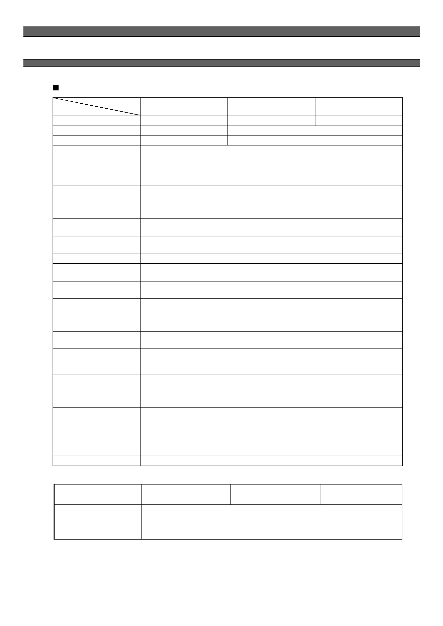
PRODUCT LINEUP
Part number
Parameter
MB90V370
MB90F372
MB90372
Classification
--
Flash type ROM
Mask ROM
ROM size
--
64K Bytes
RAM size
15.7K Bytes
6K Bytes
CPU function
Number of instruction
: 351
Minimum execution time
: 62.5 ns / 4 MHz (PLL x 4)
Addressing mode
: 23
Data bit length
: 1, 8, 16 bits
Maximum memory space
: 16 MBytes
I/O port
I/O port (N-channel)
: 16
I/O port (CMOS)
: 72
I/O port (CMOS with pull-up control) : 32
Total
: 120
16-bit reload timer
Reload timer
: 4 channels
Reload mode, single-shot mode or event count mode selectable
16-bit PPG timer
PPG timer
: 3 channels
PWM mode or single-shot mode selectable
Bit decoder
Bit decoder
: 1 channel
Parity generator
Parity generator
: 1 channel
Selectable odd/even parity
PS/2 interface
PS/2 interface
: 3 channels
4 selectable sampling clocks
LPC interface
LPC bus interface
: 1 channel
Universal peripheral Interface
: 4 channels
GA20 output control
: for UPI channel 0 only
Data buffer array
: 48 bytes
Serial IRQ controller
Serial IRQ request
: 6 channels
LPC clock monitor / control
UART
With full-duplex double buffer (variable data length)
Clock asynchronized or clock synchronized transmission (with start and stop bits) can be
selectively used
I
2
C
I
2
C (SMbus compliant)
: 1 channel
Support I
2
C bus of PHILIPS and the SMbus proposed by Intel I
2
C bus
Selectable packet error check
Timeout detection function
Multi-address I
2
C
Multi-address I
2
C (SMbus compliant) : 1 channel
Support I
2
C bus of PHILIPS and the SMbus proposed by Intel I
2
C bus
Selectable packet error check
Timeout detection function
6 addresses support
ALERT function
Bridge circuit
Three bus connection routes can be switched by I
2
C / multi-address I
2
C
Part number
Parameter
MB90V370
MB90F372
MB90372
Comparator
A comparator that can change the hysteresis width is contained
Battery voltage, mounting/dismounting and instantaneous interruption can be
detected
Parallel and serial charging/discharging
MB90370 Series
4
*: Varies with conditions such as the operating frequency (see Section
"
ELECTRICAL CHARACTERISTICS
"
).
Assurance for the MB90V370 is given only for operation with a tool at power supply voltage of 3.0 V to 3.6 V,
an operating temperature of 0 to +25 C, and an operating frequency of 1 MHz to 16 MHz.
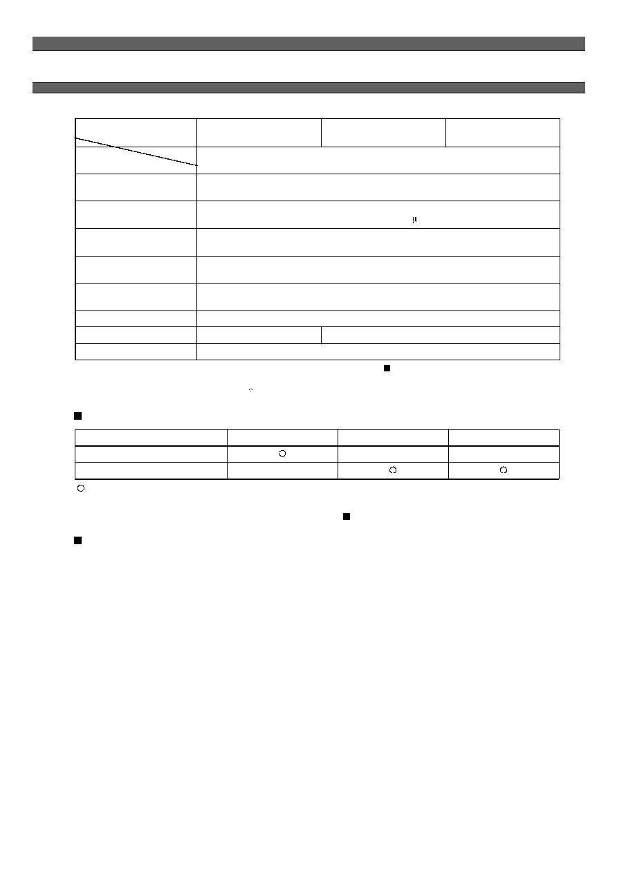
PACKAGE AND CORRESPONDING PRODUCTS
: Available
X : Not available
Note: For more information about each package, see Section
"
PACKAGE DIMENSIONS
"
.
DIFFERENCES AMONG PRODUCTS
Memory size
In evaluation with an evaluation product, note the difference between the evaluation product and the product
actually used. The following items must be taken into consideration.
�
The MB90V370 does not have an internal ROM, however, operations equivalent to chips with an internal ROM
can be evaluated by using a dedicated development tool, enabling selection of ROM size by settings of the
development tool.
�
In the MB90V370, images from FF4000
H
to FFFFFF
H
are mapped to bank 00, and FF0000
H
to FF3FFF
H
are
mapped to bank FF only. (This setting can be changed by the development tool configuration.)
�
In the MB90372/F372, images from FF4000
H
to FFFFFF
H
are mapped to bank 00, and FF0000
H
to FF3FFF
H
are mapped to bank FF only.
External
interrupt
6 independent channels
Selectable causes
: Rise/fall edge, fall edge,
"
L
"
level or
"
H
"
level
Key-on wake-up
interrupt
8 independent channels
Causes
:
"
L
"
level
8/10-bit A/D
converter
8/10-bit resolution
: 12 channels
Conversion time
: Less than 6.13 S (16 MHz internal clock)
8-bit D/A
converter
8-bit resolution
: 2 channels
LCD controller/driver
Up to 9 SEG x 4 COM
Selectable LCD output or CMOS I/O port
Low-power
consumption
Stop mode / Sleep mode / CPU intermittent operation mode / Watch mode
Process
CMOS
Package
PGA256
LQFP-144 (FPT-144P-M12: 0.4 mm pitch)
Operating voltage
3.0~3.6 V @ 16 MHz *
Package
MB90V370
MB90F372
MB90372
PGA256
X
X
FPT-144P-M12
X
Part number
Parameter
MB90V370
MB90F372
MB90372
MB90370 Series
5
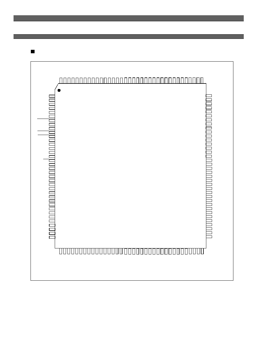
PIN ASSIGNMENT
P40/PSCK0
P41/PSDA0
P42/PSCK1
P43/PSDA1
P44/PSCK2
P45/PSDA2
P46/CLKRUN
P47/SERIRQ
P50/GA20
P51/LFRAME
P52/LRESET
P53/LCK
P54/LAD0
P55/LAD1
P56/LAD2
P57/LAD3
RST
Vcc
Vss
X0A
X1A
PA0/ALR1
PA1/ALR2
PA2/ALR3
PA3/ACO
PA4/OFB1
PA5/OFB2
PA6/OFB3
CVcc
CVRH1
CVRH2
CVRL
CVss
PB0/DCIN
PB1/DCIN2
PB2/VOL1
1
2
3
4
5
6
7
8
9
10
11
12
13
14
15
16
17
18
19
20
21
22
23
24
25
26
27
28
29
30
31
32
33
34
35
36
P
B
3
/
V
S
I
1
P
B
4
/
V
O
L
2
P
B
5
/
V
S
I
2
P
B
6
/
V
O
L
3
P
B
7
/
V
S
I
3
A
V
c
c
A
V
R
A
V
s
s
P
C
0
/
A
N
0
/
S
W
1
P
C
1
/
A
N
1
/
S
W
2
P
C
2
/
A
N
2
/
S
W
3
P
C
3
/
A
N
3
P
C
4
/
A
N
4
P
C
5
/
A
N
5
P
C
6
/
A
N
6
P
C
7
/
A
N
7
P
D
0
/
A
N
8
V
c
c
V
s
s
M
D
2
M
D
1
M
D
0
P
D
1
/
A
N
9
P
D
2
/
A
N
1
0
P
D
3
/
A
N
1
1
P
D
4
/
D
A
1
P
D
5
/
D
A
2
P
D
6
/
P
P
G
2
P
9
0
/
S
C
L
2
P
9
1
/
S
D
A
2
P
9
2
/
S
C
L
3
P
9
3
/
S
D
A
3
P
9
4
/
S
C
L
4
P
9
5
/
S
D
A
4
P
8
0
/
S
C
L
1
P
8
1
/
S
D
A
1
3
7
3
8
3
9
4
0
4
1
4
2
4
3
4
4
4
5
4
6
4
7
4
8
4
9
5
0
5
1
5
2
5
3
5
4
5
5
5
6
5
7
5
8
5
9
6
0
6
1
6
2
6
3
6
4
6
5
6
6
6
7
6
8
6
9
7
0
7
1
7
2
P77/PPG1
P76/UI3
P75/UO3
P74/UCK3
P73/UI2
P72/UO2
P71/UCK2
P70/UI1
P67/UO1
P66/UCK1
P65/INT5
P64/INT4
P63/INT3
P62/INT2
P61/INT1
P60/INT0
PD7/PPG3
Vss
Vcc
PF7/V3*
PF6/V2*
PF5/V1*
PF4/COM3*
PF3/COM2*
PF2/COM1*
PF1/COM0*
PF0/SEG8*
PE7/TO4/SEG7
PE6/TIN4/SEG6
PE5/TO3/SEG5
PE4/TIN3/SEG4
PE3/TO2/SEG3
PE2/TIN2/SEG2
PE1/TO1/SEG1
PE0/TIN1/SEG0
P82/ALERT
108
107
106
105
104
103
102
101
100
99
98
97
96
95
94
93
92
91
90
89
88
87
86
85
84
83
82
81
80
79
78
77
76
75
74
73
P
3
7
/
A
D
T
G
P
3
6
P
3
5
P
3
4
P
3
3
P
3
2
P
3
1
P
3
0
P
2
7
P
2
6
P
2
5
P
2
4
P
2
3
P
2
2
P
2
1
X
1
X
0
V
s
s
V
c
c
P
2
0
P
1
7
P
1
6
P
1
5
P
1
4
P
1
3
P
1
2
P
1
1
P
1
0
P
0
7
/
K
S
I
7
P
0
6
/
K
S
I
6
P
0
5
/
K
S
I
5
P
0
4
/
K
S
I
4
P
0
3
/
K
S
I
3
P
0
2
/
K
S
I
2
P
0
1
/
K
S
I
1
P
0
0
/
K
S
I
0
1
4
4
1
4
3
1
4
2
1
4
1
1
4
0
1
3
9
1
3
8
1
3
7
1
3
6
1
3
5
1
3
4
1
3
3
1
3
2
1
3
1
1
3
0
1
2
9
1
2
8
1
2
7
1
2
6
1
2
5
1
2
4
1
2
3
1
2
2
1
2
1
1
2
0
1
1
9
1
1
8
1
1
7
1
1
6
1
1
5
1
1
4
1
1
3
1
1
2
1
1
1
1
1
0
1
0
9
(TOP VIEW)
(FPT-144P-M12)
LQFP-144
* Heavy current pins