 | ÐлекÑÑоннÑй компоненÑ: MB90477 | СкаÑаÑÑ:  PDF PDF  ZIP ZIP |
Äîêóìåíòàöèÿ è îïèñàíèÿ www.docs.chipfind.ru
DS07-13712-4E
FUJITSU SEMICONDUCTOR
DATA SHEET
16-Bit Proprietary Microcontroller
CMOS
F
2
MC-16LX MB90470 Series
MB90473/474/477/478/F474L/F474H
s
DESCRIPTIONS
The FUJITSU MB90470 Series is a 16-bit general-purpose microcontroller designed for consumer products and
other process control applications requiring high-speed and real-time processing.
The F
2
MC-16LX CPU core instruction set retains the AT architecture of the F
2
MC*
1
family, with additional instruc-
tions for use with high-level languages, expanded addressing mode, enhanced multiply and divide instructions,
and full bit processing. Also included is a built-in 32-bit accumulator for long-word processing.
Peripheral resources built into the MB90470 series include 8/16-bit PPG, expanded I/O serial interface, UART,
10-bit A/D converter, 16-bit input-output timer, 8/16-bit up-counter, PWC timer, I
2
C*
2
interface, DTP/external
interrupt, chip select, and 16-bit reload timer.
*1 : F
2
MC is an abbreviation for FUJITSU Flexible Microcontroller, and is a registered trademark of FUJITSU, Ltd.
*2 : I
2
C license :
This product includes licensing of Philips I
2
C patents if used by the customer in an I
2
C system subject to the I
2
C
standard specifications established by Philips.
s
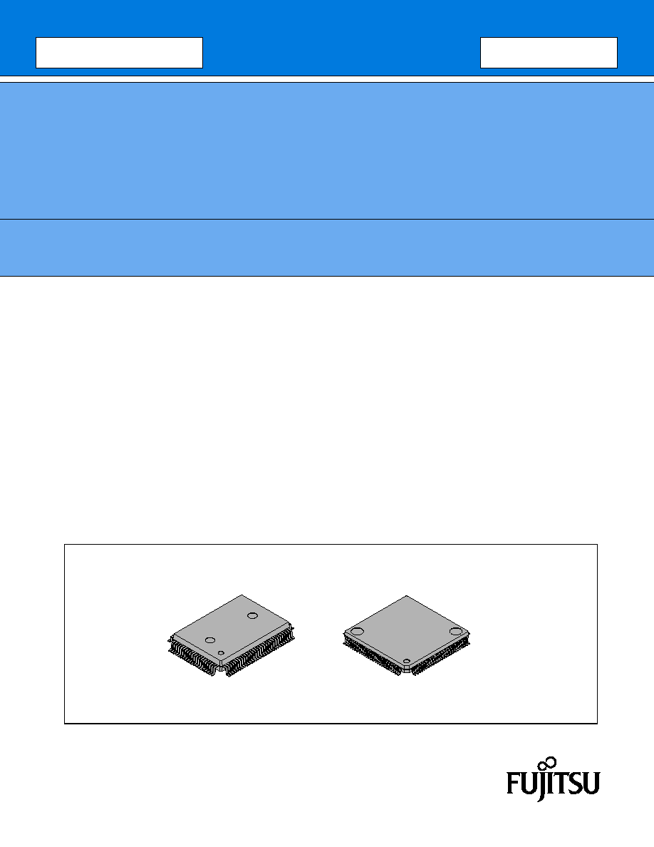
PACKAGES
100-pin plastic QFP
100-pin plastic LQFP
(FPT-100P-M06)
(FPT-100P-M05)

MB90470 Series
2
s
FEATURES
· Clocks
Minimum instruction execution time :
50.0 ns at 5 MHz base oscillation with 4
×
multiplier (internal operation at 20 MHz/3.3 V
±
0.3 V)
62.5 ns at 4 MHz base oscillation with 4
×
multiplier (internal operation at 16 MHz/3.0 V
±
0.3 V)
Uses PLL clock multiplier.
· Maximum memory size
16 Mbytes
· Instruction set optimized for control applications
Handles bit, byte, word, long-word data
23 standard addressing modes
32-bit accumulator for enhanced high-precision calculation
Signed multiply-divide and expanded RETI instructions
· Instruction system compatible with high-level language (C) multitasking
System stack pointer
Instruction set correlation and barrel shift instructions
· Non-multi bus or multi-bus compatible
· Program patch function (for two address pointers)
· Improved execution speed
4-byte queue
· Powerful interrupt functions
8 external interrupt functions with 8-level programmable priority
· Data transfer functions (
µ
µ
µ
µ
DMA or Extended intelligent I/O service)
16 channels maximum
µ
DMA maximum assured operation frequency : 16 MHz
Extended intelligent I/O service maximum assured operation frequency : 20 MHz
· Built-in ROM
Flash versions : 256 KB, Mask ROM versions : 128 KB/256 KB
· Built-in RAM
10 KB/16 KB
· General purpose ports
84 ports maximum
(includes 16 ports with input pull-up resistance setting, 14 ports with output open drain setting)
· A/D converter
RC sequential comparator type, 8 channels
10-bit resolution, conversion time 4.65
µ
s (at 20 MHz operation)
· I
2
C interface
1 channel
·
µ
µ
µ
µ
PG
1 channel
· UART
1 channel
· I/O expansion serial interface (SIO)
2 channels
· 8/16-bit up/down timer
1 channel
· 16-bit PWC
3 channels (including 2-channel input comparison function)
(Continued)

MB90470 Series
3
(Continued)
· 16-bit reload timer
1 channel (8-bit
×
2-channel, 16-bit
×
1-channel mode switching function provided)
· 16-bit input-output timer
2-channel input capture, 6-channel output compare, 1-channel free run timer
· 2 built-in clock generator systems
· Low power modes
Stop, sleep, CPU intermittent mode, watch mode, etc.
· Package options
QFP100/LQFP100
· Process
CMOS technology
· Supply voltage
Can operate on 3 V single supply systems (with 5 V interface provided by some pins with 3/5 V dual-supply
capability)
MB90470 Series
4
s
PRODUCT LINEUP
(Continued)
Parameter
Part number
MB90F474L
MB90F474H
MB90473
MB90474
ROM capacity
FLASH 256 KB
FLASH 256 KB
MASKROM
128 KB
MASKROM
256 KB
RAM capacity
16 KB
16 KB
10 KB
16 KB
CPU functions
Basic instructions
Instruction bit length
Instruction length
Data bit length
Minimum instruction execution time
: 351
: 8-bit, 16-bit
: 1 byte to 7 bytes
: 1-bit, 8-bit, 16-bit
: 62.5 ns (with 16 MHz machine clock)
Ports
General purpose input/output ports : 84 Max
General purpose input/output ports (CMOS output)
General purpose input/output ports (built-in pull-up resistance)
General purpose input/output ports (N-ch open drain)
UART
Stop-start synchronized : 1 channel
8/16-bit PPG timer
8-bit 6-channel/16-bit 3-channel
8/16-bit up-down counter/timer
Two 8-bit up-down counters with 6 event input pins
Two 8-bit reload/compare registers
16-bit
input/
out-
put
timers
16
-
bit free
-
run timer
Channel : 1
Overflow interrupt
Output compare
(
OCU
)
Channels : 6
Pin input source : from compare register match signal
Input capture (ICU)
Channels : 2
Register rewritten from pin input (rising/falling/both edges)
DTP/external interrupt circuit
External interrupt pins : 8 channels (set to edge or level correlation)
I/O expansion serial interface
2-channel, built-in
I
2
C interface
1-channel, built-in
Time base timer
18-bit counter
Interrupt cycle : 1.0 ms, 4.1 ms, 16.4 ms, 131.1 ms
(minimum times, at base oscillator frequency 4 MHz)
A/D converter
Conversion accuracy : 8/10-bit switchable
Single conversion mode (converts selected channel 1 time only)
Scan conversion mode
(converts multiple consecutive channels, programmable up to 8 channels)
Continuous conversion mode (converts selected channels continuously)
Stop conversion mode (converts selected channel, stops and repeats)
Watchdog timer
Reset interval : 3.58 ms, 14.33 ms, 57.23 ms, 458.75 ms
(minimum times, at base oscillator frequency 4 MHz)
Low power (standby) modes
Sleep, stop, CPU intermittent, watch mode
Process
CMOS
Notes
Flash model, low
voltage version
(f
=
10 MHz or
less at V
CC
=
2.4 V)
Flash model, high
voltage version
(f
=
20 MHz)
Mask version
Mask version
Emulator dedicated power supply
MB90470 Series
5
(Continued)
Parameter
Part number
MB90477
MB90478
MB90V470B
ROM capacity
MASKROM
256 KB
MASKROM
256 KB
RAM capacity
8 KB
8 KB
16 KB
CPU functions
Basic instructions
Instruction bit length
Instruction length
Data bit length
Minimum instruction execution time
: 351
: 8-bit, 16-bit
: 1 byte to 7 bytes
: 1-bit, 8-bit, 16-bit
: 50 ns (with 20 MHz
machine clock)
Ports
General purpose input/output ports : 84 Max
General purpose input/output ports (CMOS output)
General purpose input/output ports (built-in pull-up resistance)
General purpose input/output ports (N-ch open drain)
UART
Stop-start synchronized : 1 channel
8/16-bit PPG timer
8-bit 6-channel/16-bit 3-channel
8/16-bit up-down counter/timer
Two 8-bit up-down counters with 6 event input pins
Two 8-bit reload/compare registers
16-bit
input/
output
timers
16-bit free-run timer
Channel : 1
Overflow interrupt
Output compare (OCU)
Channels : 6
Pin input source : from compare register match signal
Input capture (ICU)
Channels : 2
Register rewritten from pin input (rising/falling/both edges)
DTP/external interrupt circuit
External interrupt pins : 8 channels (set to edge or level correlation)
I/O expansion serial interface
2-channel, built-in
I
2
C interface
1-channel, built-in
Time base timer
18-bit counter
Interrupt cycle : 1.0 ms, 4.1 ms, 16.4 ms, 131.1 ms
(minimum times, at base oscillator frequency 4 MHz)
A/D converter
Conversion accuracy : 8/10-bit switchable
Single conversion mode (converts selected channel 1 time only)
Scan conversion mode
(converts multiple consecutive channels, programmable up to 8 channels)
Continuous conversion mode (converts selected channels continuously)
Stop conversion mode (converts selected channel, stops and repeats)
Watchdog timer
Reset interval : 3.58 ms, 14.33 ms, 57.23 ms, 458.75 ms
(minimum times, at base oscillator frequency 4 MHz)
Low power (standby) modes
Sleep, stop, CPU intermittent, watch mode
Process
CMOS
Notes
Mask version
Mask version without
I
2
C
built-in interface
EVA function
User pin
Emulator dedicated power supply
Included
Document Outline