DS07-13716-2E
FUJITSU SEMICONDUCTOR
DATA SHEET
16-bit Proprietary Microcontroller
CMOS
F
2
MC
-
16LX MB90440G Series
MB90443G/F443G/V440G
s
DESCRIPTION
The MB90440G series with FULL-CAN
*2
and FLASH ROM is a line of general-purpose, Fujitsu 16-bit microcon-
trollers specially designed for automotive and industrial applications. Its main features are three on board CAN
Interfaces (generic type) , which conform to V2.0 Part A and Part B, supporting very flexible message buffering.
Thus, more functions than a normal full CAN approach is available.
While inheriting the AT architecture of the F
2
MC
*1
family, the instruction set for the F
2
MC-16LX CPU core incor-
porates additional instructions for high-level languages, supports extended addressing modes, and contains
enhanced multiplication and division instructions as well as a substantial collection of improved bit manipulation
instructions. In addition, the MB90440G series has as on-chip 32-bit accumulator, which enables processing of
long-word data.
The peripheral resources integrated in the MB90440G series include; an 8/10-bit A/D converter, UARTs (SCI) ,
I/O extended serial interface, 8/16-bit PPG timer, input/output timer (input capture (ICU) , output compare (OCU) ) .
*1 : F
2
MC stands for FUJITUS Flexible Microcontroller, a registered trademark of FUJITSU LIMITED.
*2 : Controller Area Network (CAN) is a license of Robert Bosch GmbH..
s
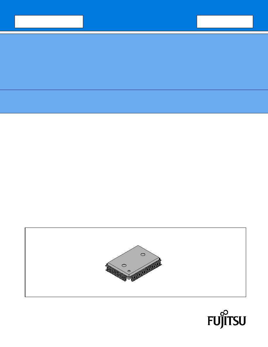
PACKAGE
100-pin Plastic QFP
FPT-100P-M06

MB90440G Series
2
s
FEATURES
∑
∑
∑
∑
Clock
Internal PLL clock multiplication circuit
Base oscillation divided into two or multiplied by one to four
Minimum execution time : 62.5 ns (4 MHz oscillation, PLL clock multiplication multiplier
=
4, V
CC
=
5.0 V)
32 kHz subsystem clock
∑
∑
∑
∑
Instruction set optimized for controller applications
Supported data types : bit, byte, word, and long-word types
Standard addressing modes : 23 types
Singed multiplication/division and extended RET1 instructions
32-bit accumulator enhancing high-precision operations
∑
∑
∑
∑
Enhanced high level language (C) and multi-tasking support instructions
Use of a system stack pointer
Symmetrical instruction set and barrel shift instructions
∑
∑
∑
∑
Program patch function (for two address pointers)
∑
∑
∑
∑
Enhanced execution speed : 4 byte instruction queue
∑
∑
∑
∑
Enhanced interrupt function : 8 priority levels programmable and 34 causes
∑
∑
∑
∑
Automatic data transmission function independent of CPU operation
Extended intelligent I/O service function (EI
2
OS)
∑
∑
∑
∑
Internal ROM size and type
FLASH ROM : 128 Kbytes
Internal RAM size : 6 Kbyte and 14 Kbyte (evaluation chip)
∑
∑
∑
∑
FLASH ROM
Supports automatic programming function, Embedded Algorithm*
Writing command/erase command/erase suspend and resume command
Algorithms completion flag
Hardwire reset vector to show the fixed boot code sector
Can be erased by each sector
Sector protection by external programming voltage
∑
∑
∑
∑
Low-power consumption (stand-by) modes
Sleep mode (CPU operating clock stops)
Stop mode (Main oscillation stops)
CPU intermittent operation mode
Watch mode
Time-base timer mode
∑
∑
∑
∑
General-purpose I/O ports : 81 ports
∑
∑
∑
∑
Timers
Watchdog timer : 1 channel
8/16-bit PPG timer : 8/16-bit
◊
4 channels
16-bit reload timer : 2 channels
* : Embedded Algorithm is a trademark of Advanced Micro Devices, Inc.
(Continued)

MB90440G Series
3
(Continued)
∑
∑
∑
∑
16-bit I/O timers
16-bit free-run timers : 1 channel
16-bit input capture : 8 channels
16-bit output compare : 4 channels
∑
∑
∑
∑
Extended I/O serial interfaces : 1 channel
∑
∑
∑
∑
UART0
Full-duplex, double-buffered (8 bit)
Can be used for clock synchronous and asynchronous transfer (with start/stop bit)
∑
∑
∑
∑
UART1 (SCI)
Full-duplex, double-buffered (8 bit)
Can be used for clock synchronous and asynchronous serial transfer (extended I/O serial)
∑
∑
∑
∑
External interrupt inputs : 8 channels
Extended intelligent I/O service (EI
2
OS) is started by external input and external interrupt generation module
∑
∑
∑
∑
Delayed interrupt generation module : interrupt request for task switching
∑
∑
∑
∑
8/10 bit A/D converter : 8 channels
8/10-bit resolution selectable
Can be started by external trigger input
Conversion time : 6.12
µ
s
∑
∑
∑
∑
FULL-CAN interface
3 channels
Conform to V2.0 Part A and Part B
Supports very flexible message buffering (mail-box and FIFO buffering can be mixed)
∑
∑
∑
∑
External bus interface : maximum 16 Mbyte address space

MB90440G Series
4
s
PRODUCT LINEUP
The following table provides a quick outlook of the MB90440G Series
(Continued)
Part number
MB90443G
(under development)
MB90F443G
MB90V440G
Parameter
CPU
F
2
MC-16LX CPU
System clock
On-chip PLL clock multiplier (
◊
1,
◊
2,
◊
3,
◊
4, 1/2 when PLL stops)
Minimum instruction execution time : 62.5 ns (4 MHz osc. PLL
◊
4)
ROM size
Mask ROM
128 Kbytes
Flash memory
128 Kbytes
External
RAM size
6 Kbytes
6 Kbytes
14 Kbytes
Operating
*1
voltage range
5 V
±
10
%
Temperature range
-
40
∞
C to
+
105
∞
C
Package
QFP100
PGA-256
Voltage dedicated for
emulator
*2
No
UART0
Full duplex double buffer
Supports clock asynchronous/synchronous (with start/stop bits) transfer
Baud rate : 4808/5208/9615/10417/19230/38460/62500/500000 bps (asynchronous)
500 K/1 M/2 Mbps (synchronous) at System clock
=
16 MHz
UART1
(SCI)
Full duplex double buffer
Asynchronized (start/stop bits synchronized) and CLK-synchronous communication
Baud rate : 601 bps to 250 kbps (asynchronous)
31.25 kbps to 2 Mbps (synchronous)
Serial IO
Transfer can be started from MSB or LSB
Supports internal clock synchronized transfer and external clock synchronized transfer
Supports positive-edge and negative-edge clock synchronization
Baud rate : 31.25 K/62.5 K/125 K/500 K/1 M/2 Mbps at System clock
=
16 MHz
8/10 bit
A/D Converter
10-bit or 8-bit resolution
8 input channels
Conversion time : 6.12
µ
s (per one channel)
16-bit Reload Timer
(2 channels)
Operation clock frequency : fsys/2
1
, fsys/2
3
, fsys/2
5
(fsys
=
System clock frequency)
Supports External Event Count function
16-bit
I/O Timer
Signals an interrupt during overflow
Supports Timer Clear during a match with Output Compare (Channel 0)
Operation clock freq. : fsys/2
2
, fsys/2
4
, fsys/2
6
, fsys/2
8
(fsys
=
System clock freq.)
16-bit
Output Compare
(4 channels)
Signals an interrupt during a match with 16-bit I/O Timer
Four 16-bit compare registers
A pair of compare registers can be used to generate an output signal
MB90440G Series
5
(Continued)
*1 : Values with conditions such as the operating frequency (See section " ELECTRICAL CHARACTERISTICS") .
*2 : DIP switch S2 when using emulation pad MB2145-507.
The details are referred to hardware manual of MB2145-507.
Part number
MB90443G
(under development)
MB90F443G
MB90V440G
Parameter
16-bit
Input Capture
(8 channels)
Rising edge, falling edge or rising & falling edge sensitive
Four 16-bit capture registers
Signals an interrupt upon external event
8/16-bit
Programmable Pulse
Generator
(4 channels)
Supports 8-bit and 16-bit operation modes
Eight 8-bit reload counters
Eight 8-bit reload registers for L pulse width
Eight 8-bit reload registers for H pulse width
A pair of 8-bit reload counters can be configured as one 16-bit reload counter or as
8-bit prescaler plus 8-bit reload counter
4 output pins
Operation clock frequency. : fsys, fsys/2
1
, fsys/2
2
, fsys/2
3
, fsys/2
4
or 128
µ
s@fosc
=
4 MHz
(fsys
=
System clock frequency, fosc
=
Oscillation clock frequency)
CAN Interface
3 channels :
Conforms to CAN Specification Version 2.0 Part A and B
Automatic re-transmission in case of error
Automatic transmission responding to Remote Frame
Supports prioritized 16 message buffers for data and ID
Flexible configuration of acceptance filtering :
Full bit compare / Full bit mask / Two partial bit masks
Supports up to 1 Mbps
External Interrupt
(8 channels)
Can be programmed edge detection or level detection
External bus interface
The external access used selective 8-bit bus or 16-bit bus is available.
(External bus mode)
I/O Ports
Virtually all external pins can be used as general purpose I/O
All push-pull outputs and schmitt trigger inputs
Bit-wise programmable as input/output or peripheral signal
32 kHz Subclock
Sub-clock for low power operation
Flash
Memory
Supports automatic programming, Embedded Algorithm
TM
Write/Erase/Erase-Suspend/Resume commands
A flag indicating completion of the algorithm
Number of erase cycles : 10,000 times
Data retention time : 10 years
Boot block configuration
Erase can be performed on each block
Block protection with external programming voltage