
DS07-13702-4E
FUJITSU SEMICONDUCTOR
DATA SHEET
16-bit Proprietary Microcontroller
CMOS
F
2
MC-16LX MB90520 Series
MB90522/523/F523/V520
s
DESCRIPTION
The MB90520 series is a general-purpose 16-bit microcontroller developed and designed by Fujitsu for process
control applications in consumer products that require high-speed real-time processing.
The instruction set of the F
2
MC-16LX CPU core inherits AT architecture of the F
2
MC* family with additional
instruction sets for high-level languages, extended addressing mode, enhanced multiplication/division
instructions, and enhanced bit manipulation instructions. The microcontroller has a 32-bit accumulator for
processing long word data.
The MB90520 series has peripheral resources of 8/10-bit A/D converter, 8-bit D/A converter, UART (SCI),
extended I/O serial interfaces 0 and 1, 8/16-bit up/down counter/timers 0 and 1, 8/16-bit PPG timers 0 and 1,
I/O timer (16-bit free-run timers 1 and 2, input captures 0 and 1 (ICU), output compares 0 and 1 (OCU)), and
an LCD controller/driver.
*:F
2
MC stands for FUJITSU Flexible Microcontroller, a registered trademark of FUJITSU LIMITED.
s
FEATURES
� Clock
Embedded PLL clock multiplication circuit
Operating clock (PLL clock) can be selected from divided-by-2 of oscillation or one to four times the oscillation
(at oscillation of 4 MHz, 4 MHz to 16 MHz).
The system can be operated by a sub-clock (rated at 32.768 kHz).
Minimum instruction execution time: 62.5 ns (at oscillation of 4 MHz, four times the oscillation clock, operation
at V
CC
of 5.0 V)
(Continued)
s
PACKAGES
120-pin Plastic LQFP
(FPT-120P-M05)
120-pin Plastic QFP
(FPT-120P-M13)

MB90520 Series
2
(Continued)
� Maximum memory space
16 Mbytes
� Instruction set optimized for controller applications
Rich data types (bit, byte, word, long word)
Rich addressing mode (23 types)
Enhanced signed multiplication/division instruction and RETI instruction functions
Enhanced precision calculation realized by 32-bit accumulator
� Instruction set designed for high level language (C) and multi-task operations
Adoption of system stack pointer
Enhanced pointer indirect instructions
Barrel shift instructions
� Program patch function (for two address pointers)
� Enhanced execution speed
4-byte instruction queue
� Enhanced interrupt function
8 levels, 34 factors
� Automatic data transmission function independent of CPU operation
Extended intelligent I/O service function (EI
2
OS): Up to 16 channels
� Embedded ROM size and types
Mask ROM: 64 kbytes/128 kbytes
Flash ROM: 128 kbytes
� Embedded RAM size
Mask ROM: 4 kbytes
Flash ROM: 4 kbytes
Evaluation product: 6 kbytes
� Low-power consumption (stand-by) mode
Sleep mode (mode in which CPU operating clock is stopped)
Stop mode (mode in which oscillation is stopped)
CPU intermittent operation mode
Hardware stand-by mode
Clock mode (mode in which other than sub-clock and timebase timer are stopped)
� Process
CMOS technology
� I/O port
General-purpose I/O ports (CMOS): 53 ports
General-purpose I/O ports (via pull-up resistors): 24 ports
General-purpose I/O ports (open-drain): 8 ports
Total: 85 ports
� Timer
Timebase timer/watchdog timer: 1 channel
8/16-bit PPG timers 0, 1: 8-bit
�
2 channels or 16-bit
�
1 channel
� 16-bit re-load timers 0, 1: 2 channels
(Continued)

MB90520 Series
3
(Continued)
� 16-bit I/O timer
16-bit free-run timers 1, 2: 2 channels
Input captures 0, 1 (ICU): Generates an interrupt request by latching a 16-bit free-run timer counter value upon
detection of an edge input to the pin.
Output compares 0, 1 (OCU): Generates an interrupt request and reverses the output level upon detection of a
match between the 16-bit free-run timer counter value and the compare setting
value.
8/16-bit up/down counter/timers 0, 1: 1 channel (8-bit
�
2 channels)
� Extended I/O serial interfaces 0, 1: 1 channel
� UART (SCI)
With full-duplex double buffer
Clock asynchronized or clock synchronized transmission can be selectively used.
� DTP/external interrupt circuit (8 channels)
A module for starting extended intelligent I/O service (EI
2
OS) and generating an external interrupt triggered
by an external input.
� Wake-up interrupt
Receives external interrupt requests and generates an interrupt request upon an "L" level input.
� Delayed interrupt generation module
Generates an interrupt request for switching tasks.
� 8/10-bit A/D converter (8 channels)
8/10-bit resolution can be selectively used.
Starting by an external trigger input.
Conversion time: minimum 15.0
�
s (at machine clock frequency of 16 MHz, including sampling time)
� 8-bit D/A converter (based on the R-2R system)
8-bit resolution: 2 channels (independent)
Setup time: 12.5
�
s
� Clock timer: 1 channel
� LCD controller/driver
A common driver and a segment driver that can directly drive the LCD (liquid crystal display) panel
� Clock output function
Note: Do not set external bus mode for the MB90520 series because it cannot be operated in this mode.
MB90520 Series
4
s
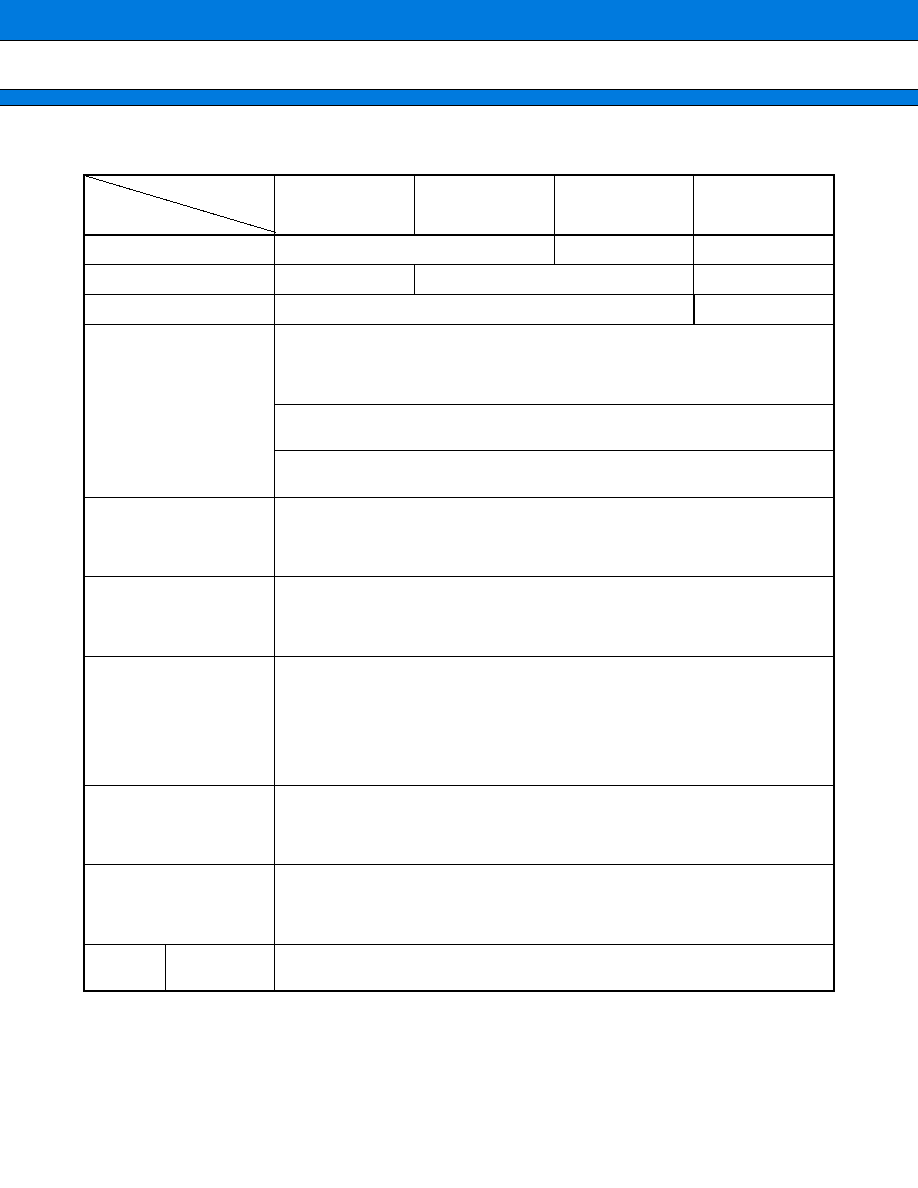
PRODUCT LINEUP
(Continued)
MB90522
MB90523
MB90F523
MB90V520
Classification
Mask ROM product
Flash ROM product Evaluation product
ROM size
64 kbytes
128 kbytes
None
RAM size
4 kbytes
6 kbytes
CPU functions
Number of instructions: 351
Instruction bit length: 8 bits, 16 bits
Instruction length: 1 byte to 7 bytes
Data bit length: 1 bit, 8 bits, 16 bits
Minimum execution time: 62.5 ns
(at machine clock frequency of 16 MHz)
Interrupt processing time: 1.5
�
s
(at machine clock frequency of 16 MHz, minimum value)
Ports
General-purpose I/O ports (CMOS output): 53
General-purpose I/O ports (via pull-up resistor): 24
General-purpose I/O ports (N-ch open-drain output): 8
Total: 85
UART (SCI)
Clock synchronized transmission (62.5 kbps to 1 Mbps)
Clock asynchronized transmission (1202 bps to 9615 bps)
Transmission can be performed by bi-directional serial transmission or by
master/slave connection.
8/10-bit A/D converter
Conversion precision: 8/10-bit can be selectively used.
Number of inputs: 8
One-shot conversion mode (converts selected channel only once)
Scan conversion mode (converts two or more successive channels and can
program up to 8 channels.)
Continuous conversion mode (converts selected channel continuously)
Stop conversion mode (converts selected channel and stop operation repeatedly)
8/16-bit PPG timers 0, 1
Number of channels: 1 (8-bit
�
2 channels)
PPG operation of 8-bit or 16-bit
Pulse wave of given intervals and given duty ratios can be output.
Pulse interval: 62.5 ns to 1
�
s (at machine clock frequency of 16 MHz)
8/16-bit up/down counter/
timers 0, 1
Number of channels: 1 (8-bit
�
2 channels)
Event input: 6 channels
8-bit up/down counter/timer used: 2 channels
8-bit re-load/compare function supported: 1 channel
16-bit
I/O timer
16-bit free-run
timers 1, 2
Number of channels: 2
Overflow interrupts
Item
Part number
MB90520 Series
5
(Continued)
* : Varies with conditions such as the operating frequency. (See section "
s
Electrical Characteristics.")
Assurance for the MB90V520 is given only for operation with a tool at a power voltage of 3.0 V to 5.5 V, an
operating temperature of 0 to 55 degrees centigrade, and an operating frequency of 1 MHz to 16 MHz.
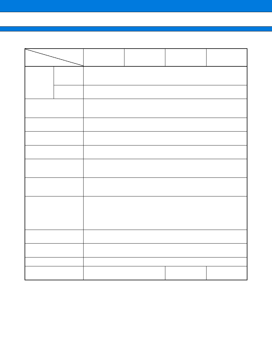
Part number
MB90523
MB90523
MB90F523
MB90V520
Item
16-bit
I/O timer
Output
compares 0, 1
(OCU)
Number of channels: 8
Pin input factor: Match signal of compare register
Input captures
0, 1 (ICU)
Number of channels: 2
Rewriting register value upon pin input (rising, falling, or both edges)
DTP/external interrupt circuit
Number of inputs: 8
Started by rising edge, falling edge, "H" level input, or "L" level input.
External interrupt circuit or extended intelligent I/O service (EI
2
OS) can be used.
Wake-up intrrupt
Number of inputs: 8
Started by "L" level input.
Delayed interrupt generation
module
Interrupt generation module for switching tasks
Used in real-time operating systems.
Extended I/O serial
interfaces 0, 1
Clock synchronized transmission (3125 bps to 1 Mbps)
LSB first/MSB first
Timebase timer
18-bit counter
Interrupt interval: 1.024 ms, 4.096 ms, 16.384 ms, 131.072 ms
(at oscillation of 4 MHz)
8-bit D/A converter
8-bit resolution
Number of channels: 2 channels
Based on R-2R system
LCD controller/driver
Number of common output pins: 4
Number of segment output pins: 32
Number of power supply pins for LCD drive: 4
RAM for LCD indication: 16 bytes
Booster for LCD drive: Internal
Split resistor for LCD drive: Internal
Watchdog timer
Reset generation interval: 3.58 ms, 14.33 ms, 57.23 ms, 458.75 ms
(at oscillation of 4 MHz, minimum value)
Low-power consumption
(stand-by) mode
Sleep/stop/CPU intermittent operation/clock timer/hardware stand-by
Process
CMOS
Power supply voltage for
operation*
3.0 V to 5.5 V
4.0 V to 5.5 V
3.0 V to 5.5 V