DS07-13703-3E
FUJITSU SEMICONDUCTOR
DATA SHEET
16-bit Proprietary Microcontroller
CMOS
F
2
MC-16LX MB90540/G/545/G Series
MB90F543/F549/V540
MB90F543G(S)/F546G(S)/F548G(S)/F549G(S)/549G(S)/V540G
s
s
s
s
DESCRIPTION
The MB90540/545 series with FULL-CAN*
1
and FLASH ROM is specially designed for automotive and industrial
applications. Its main features are two on board CAN Interfaces (one for MB90V545 series) , which conform to
V2.0 Part A and Part B, supporting very flexible message buffer
scheme and so offering more functions than a
normal full CAN approach. The instruction set by F
2
MC-16LX CPU core inherits an AT architecture of the F
2
MC*
2
family with additional instruction sets for high-level languages, extended addressing mode, enhanced multiplica-
tion/division instructions, and enhanced bit manipulation instructions.The micro controller has a 32-bit accumulator
for processing long word data.The MB90540/545 series has peripheral resources of 8/10-bit A/D converters,
UART (SCI) , extended I/O serial interfaces, 8/16-bit timer, I/O timer (input capture (ICU) , output compare (OCU) ) .
*1 : Controller Area Network (CAN) -License of Robert Bosch GmbH.
*2 : F
2
MC stands for FUJITSU Flexible Microcontroller.
s
s
s
s
FEATURES
∑ Clock
Embedded PLL clock multiplication circuit
Operating clock (PLL clock) can be selected from : divided-by-2 of oscillation or one to four times the oscillation
Minimum instruction execution time : 62.5 ns (operation at oscillation of 4 MHz, four times the oscillation clock,
V
CC
of 5.0 V)
Subsystem Clock : 32 kHz
(Continued)
s
s
s
s
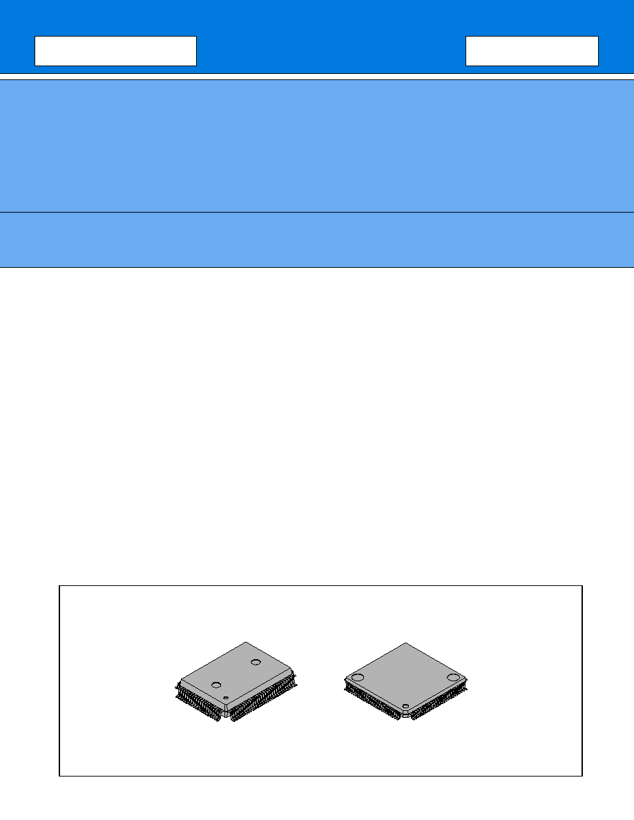
PACKAGES
100-pin Plastic QFP
100-pin Plastic LQFP
(FPT-100P-M06)
(FPT-100P-M05)

MB90540/540G/545/545G Series
2
(Continued)
∑ Instruction set to optimize controller applications
Rich data types (bit, byte, word, long word)
Rich addressing mode (23 types)
Enhanced signed multiplication/division instruction and RETI instruction functions
Enhanced precision calculation realized by the 32-bit accumulator
∑ Instruction set designed for high level language (C language) and multi-task operations
Adoption of system stack pointer
Enhanced pointer indirect instructions
Barrel shift instructions
∑ Program patch function (for two address pointers)
∑ Enhanced execution speed : 4-byte Instruction queue
∑ Enhanced interrupt function : 8 levels, 34 factors
∑ Automatic data transmission function independent of CPU operation
Extended intelligent I/O service function (EI
2
OS)
∑ Embedded ROM size and types
Mask ROM : 256 Kbytes
Flash ROM : 128 Kbytes/256 Kbytes
Embedded RAM size : 4 Kbytes/6 Kbytes/8 Kbytes (evaluation chip)
∑ Flash ROM
Supports automatic programming, Embedded Algorithm TM*
Write/Erase/Erase-Suspend/Resume commands
A flag indicating completion of the algorithm
Hard-wired reset vector available in order to point to a fixed boot sector in Flash Memory
Erase can be performed on each block
Block protection with external programming voltage
∑ Low-power consumption (stand-by) mode
Sleep mode (mode in which CPU operating clock is stopped)
Stop mode (mode in which oscillation is stopped)
CPU intermittent operation mode
Clock mode
Hardware stand-by mode
∑ Process
0.5
µ
m CMOS technology
∑ I/O port
General-purpose I/O ports : 81 ports
∑ Timer
Watchdog timer : 1 channel
8/16-bit PPG timer : 8/16-bit
◊
4 channels
16-bit re-load timer : 2 channels
∑ 16-bit I/O timer
16-bit free-run timer : 1 channel
Input capture : 8 channels
Output compare : 4 channels
∑ Extended I/O serial interface : 1 channel
∑ UART 0
With full-duplex double buffer (8-bit length)
Clock asynchronized or clock synchronized (with start/stop bit) transmission can be selectively used.
(Continued)

MB90540/540G/545/545G Series
3
(Continued)
∑ UART 1
With full-duplex double buffer (8-bit length)
Clock asynchronized or clock synchronized serial (extended I/O serial) can be used.
∑ External interrupt circuit (8 channels)
A module for starting an extended intelligent I/O service (EI
2
OS) and generating an external interrupt which
is triggered by an external input.
∑ Delayed interrupt generation module
Generates an interrupt request for switching tasks.
∑ 8/10-bit A/D converter (8 channels)
8/10-bit resolution can be selectively used.
Starting by an external trigger input.
Conversion time : 26.3
µ
s
∑ FULL-CAN interfaces
MB90540 series : 2 channel
MB90545 series : 1 channel
Conforming to Version 2.0 Part A and Part B
Flexible message buffering (mailbox and FIFO buffering can be mixed)
∑ External bus interface : Maximum address space 16 Mbytes
∑ Package: QFP-100, LQFP-100
* : Embedded Algorithm is a trade mark of Advanced Micro Devices Inc.

MB90540/540G/545/545G Series
4
s
s
s
s
PRODUCT LINEUP
(Continued)
Features
MB90V540
MB90V540G
MB90F543/F549
MB90F543G (S) /F548G (S)
MB90F549G (S) /F546G (S)
MB90549G (S)
CPU
F
2
MC-16LX CPU
System clock
On-chip PLL clock multiplier (
◊
1,
◊
2,
◊
3,
◊
4, 1/2 when PLL stop)
Minimum instruction exection time : 62.5 ns (4 MHz osc. PLL
◊
4)
ROM
External
Flash memory
MB90F543/F543G (S) /
F548G (S) : 128 K
MB90F549/F549G (S) /
F546G (S) : 256 K
Mask ROM : 256 K
RAM
8 Kbyte
MB90F548G(S):4 Kbyte
MB90F543/F549/F543G (S)
/F549G (S) : 6 Kbyte
MB90F546G (S) : 8 Kbyte
6 Kbyte
Clocks
Two clocks/One clock
*1
system
MB90F543/F549/F543G/
F548G/F549G/F546G
: Two clocks system
MB90F543GS/F548GS/
F549GS/F546GS
: One clock system
MB90549G
: Two clocks system
MB90549GS
: One clock system
Operating voltage
range
5 V
±
10
%
Temperature range
MB90F543/F549:
-
40
∞
C to 85
∞
C
Other than MB90F543/F549:
-
40
∞
C to 105
∞
C
Package
PGA-256
QFP100, LQFP100
Emulator-specify
power supply
*2
None
UART0
Full duplex double buffer
Support asynchronous/synchronous (with start/stop bit) transfer
Baud rate : 4808/5208/9615/10417/19230/38460/62500/500000 bps (asynchronous)
500 K/1 M/2 Mbps (synchronous) at System clock
=
16 MHz
UART1
(SCI)
Full duplex double buffer
Asynchronous (start-stop synchronized) and CLK-synchronous communication
Baud rate : 1202/2404/4808/9615/31250 bps (asynchronous)
62.5 K/12 K/250 K/500 K/1 M/2 Mbps (synchronous) at 6, 8, 10, 12, 16 MHz
Serial IO
Transfer can be started from MSB or LSB
Supports internal clock synchronized transfer and external clock synchronized transfer
Supports positive-edge and nagative-edge clock synchronization
Baud rate : 31.25 K/62.5 K/125 K/500 K/1 Mbps at System clock
=
16 MHz
A/D Converter
10-bit or 8-bit resolution
8 input channels
Conversion time : 26.3 ms (per one channel)
16-bit Reload Timer
(2 channels)
Operation clock frequency : fsys/2
1
, fsys/2
3
, fsys/2
5
(fsys
=
System clock frequency)
Supports External Event Count function
Signals an interrupt when overflow

MB90540/540G/545/545G Series
5
(Continued)
*1 : If the one clock system is used, equip X0A and X1A with clocks from the tool side.
*2 : It is setting of DIP switch S2 when Emulator pod (MB2145-507) is used.Please refer to the MB2145-507 hardware
manual (2.7 Emulator-specific Power Pin) about details.
*3 : Embedded Algorithm is a trade mark of Advanced Micro Devices Inc.
Features
MB90V540
MB90V540G
MB90F543/F549
MB90F543G (S) /F548G (S)
MB90F549G (S) /F546G (S)
MB90549G (S)
16-bit IO Timer
Supports Timer Clear when a match with Output Compare (Channel 0)
Operation clock freq. : fsys/2
2
, fsys/2
4
, fsys/2
6
, fsys/2
8
(fsys
=
System clock freq.)
16-bit Output Compare
(4 channels)
Signals an interrupt when a match with 16-bit IO Timer
Four 16-bit compare registers
A pair of compare registers can be used to generate an output signal
16-bit Input Capture
(8 channels)
Rising edge, falling edge or rising & falling edge sensitive
Four 16-bit Capture registers
Signals an interrupt upon external event
8/16-bit
Programmable
Pulse Generator
(4 channels)
Supports 8-bit and 16-bit operation modes
Eight 8-bit reload counters
Eight 8-bit reload registers for L pulse width
Eight 8-bit reload registers for H pulse width
A pair of 8-bit reload counters can be configured as one 16-bit reload counter or as 8-bit
prescaler plus 8-bit reload counter
4 output pins
Operation clock freq. : fsys, fsys/2
1
, fsys/2
2
, fsys/2
3
, fsys/2
4
or 128
µ
s@fosc
=
4 MHz
(fsys
=
System clock frequency, fosc
=
Oscillation clock frequency)
CAN Interface
MB90540 series
: 2 channels
MB90545 series
: 1 channel
Conforms to CAN Specification Version 2.0 Part A and B
Automatic re-transmission in case of error
Automatic transmission responding to Remate Frame
Prioritized 16 massage buffers for data and ID's
Supports multipe massages
Flexible configuration of acceptance filtering :
Full bit compare/Full bit mask/Two partial bit masks
Supports up to 1 Mbps
32 kHz Sub-clock
Sub-clock for low power operation
External Interrupt
(8 channels)
Can be programmed edge sensitive or level sensitive
External bus
interface
External access using the selectable 8-bit or 16-bit bus is enabled
(external bus mode.)
IO Ports
Virtually all external pins can be used as general purpose IO
All push-pull outputs and schmitt trigger inputs
Bit-wise programmable as input/output or peripheral signal
Flash Memory
Flash Memory Supports automatic programming, Embeded Algorithm TM
*3
Write/Erase/Erase-Suspend/Resume commands
A flag indicating completion of the algorithm
Number of erase cycles : 10,000 times
Data retention time : 10 years
Boot block configuration
Erase can be performed on each block
Block protection by externally programmed voltage