DS07-13703-5E
FUJITSU SEMICONDUCTOR
DATA SHEET
16-bit Proprietary Microcontroller
CMOS
F
2
MC-16LX MB90540/G/545/G Series
MB90F543/F549/V540
MB90F543G(S)/F546G(S)/F548G(S)/F549G(S)/549G(S)/V540G
MB90543G(S)/547G(S)/548G(S)/F548GL(S)
s
s
s
s
DESCRIPTION
The MB90540/545 series with FULL-CAN*
1
and FLASH ROM is specially designed for automotive and industrial
applications. Its main features are two on board CAN Interfaces (one for MB90V545 series) , which conform to
V2.0 Part A and Part B, supporting very flexible message buffer
scheme and so offering more functions than a
normal full CAN approach. The instruction set by F
2
MC-16LX CPU core inherits an AT architecture of the F
2
MC*
2
family with additional instruction sets for high-level languages, extended addressing mode, enhanced multiplica-
tion/division instructions, and enhanced bit manipulation instructions.The micro controller has a 32-bit accumulator
for processing long word data.The MB90540/545 series has peripheral resources of 8/10-bit A/D converters,
UART (SCI) , extended I/O serial interfaces, 8/16-bit timer, I/O timer (input capture (ICU) , output compare (OCU) ) .
*1 : Controller Area Network (CAN) -License of Robert Bosch GmbH.
*2 : F
2
MC stands for FUJITSU Flexible Microcontroller.
s
s
s
s
FEATURES
∑ Clock
Embedded PLL clock multiplication circuit
Operating clock (PLL clock) can be selected from : divided-by-2 of oscillation or one to four times the oscillation
Minimum instruction execution time : 62.5 ns (operation at oscillation of 4 MHz, four times the oscillation clock)
Subsystem Clock : 32 kHz
(Continued)
s
s
s
s
PACKAGES
(Continued)
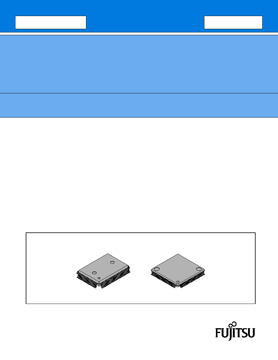
100-pin Plastic QFP
100-pin Plastic LQFP
(FPT-100P-M06)
(FPT-100P-M05)

MB90540/540G/545/545G Series
2
∑ Instruction set to optimize controller applications
Rich data types (bit, byte, word, long word)
Rich addressing mode (23 types)
Enhanced signed multiplication/division instruction and RETI instruction functions
Enhanced precision calculation realized by the 32-bit accumulator
∑ Instruction set designed for high level language (C language) and multi-task operations
Adoption of system stack pointer
Enhanced pointer indirect instructions
Barrel shift instructions
∑ Program patch function (for two address pointers)
∑ Enhanced execution speed : 4-byte Instruction queue
∑ Enhanced interrupt function : 8 levels, 34 factors
∑ Automatic data transmission function independent of CPU operation
Extended intelligent I/O service function (EI
2
OS)
∑ Embedded ROM size and types
Mask ROM : 256 Kbytes / 64 Kbytes / 128 Kbytes
Flash ROM : 128 Kbytes/256 Kbytes
Embedded RAM size : 2 Kbytes/4 Kbytes/6 Kbytes/8 Kbytes (evaluation chip)
∑ Flash ROM
Supports automatic programming, Embedded Algorithm TM*
Write/Erase/Erase-Suspend/Resume commands
A flag indicating completion of the algorithm
Hard-wired reset vector available in order to point to a fixed boot sector in Flash Memory
Erase can be performed on each block
Block protection with external programming voltage
∑ Low-power consumption (stand-by) mode
Sleep mode (mode in which CPU operating clock is stopped)
Stop mode (mode in which oscillation is stopped)
CPU intermittent operation mode
Clock mode
Hardware stand-by mode
∑ Process
0.5
µ
m CMOS technology
∑ I/O port
General-purpose I/O ports : 81 ports
∑ Timer
Watchdog timer : 1 channel
8/16-bit PPG timer : 8/16-bit
◊
4 channels
16-bit re-load timer : 2 channels
∑ 16-bit I/O timer
16-bit free-run timer : 1 channel
Input capture : 8 channels
Output compare : 4 channels
∑ Extended I/O serial interface : 1 channel
∑ UART 0
With full-duplex double buffer (8-bit length)
Clock asynchronized or clock synchronized (with start/stop bit) transmission can be selectively used.
(Continued)

MB90540/540G/545/545G Series
3
(Continued)
∑ UART 1
With full-duplex double buffer (8-bit length)
Clock asynchronized or clock synchronized serial (extended I/O serial) can be used.
∑ External interrupt circuit (8 channels)
A module for starting an extended intelligent I/O service (EI
2
OS) and generating an external interrupt which
is triggered by an external input.
∑ Delayed interrupt generation module
Generates an interrupt request for switching tasks.
∑ 8/10-bit A/D converter (8 channels)
8/10-bit resolution can be selectively used.
Starting by an external trigger input.
Conversion time : 26.3
µ
s
∑ FULL-CAN interfaces
MB90540 series : 2 channel
MB90545 series : 1 channel
Conforming to Version 2.0 Part A and Part B
Flexible message buffering (mailbox and FIFO buffering can be mixed)
∑ External bus interface : Maximum address space 16 Mbytes
∑ Package: QFP-100, LQFP-100
* : Embedded Algorithm is a trade mark of Advanced Micro Devices Inc.

MB90540/540G/545/545G Series
4
s
s
s
s
PRODUCT LINEUP
(Continued)
Features
MB90F543/F549
MB90F543G (S) /F548G (S)
MB90F549G (S) /F546G (S)
MB90F548GL(S)
MB90543G (S) *
1
MB90547G (S) *
1
MB90548G (S)
MB90549G (S)
MB90V540/V540G
CPU
F
2
MC-16LX CPU
System clock
On-chip PLL clock multiplier (
◊
1,
◊
2,
◊
3,
◊
4, 1/2 when PLL stop)
Minimum instruction exection time : 62.5 ns (4 MHz osc. PLL
◊
4)
ROM
Flash memory
MB90F543/F543G(S)/
F548G(S) / F548GL(S) :
128 K
MB90F549/F549G(S)/
F546G(S) : 256 K
Mask ROM :
MB90547G(S): 64 K
MB90543G(S)/548G(S):
128 K
MB90549G(S): 256 K
External
RAM
MB90F548G(S)/F548GL(S):
4 Kbytes
MB90F543/F549/F543G (S) /
F549G(S) : 6 Kbytes
MB90F546G(S) : 8 Kbytes
MB90547G(S): 2 Kbytes
MB90548G(S): 4 Kbytes
MB90543G(S)/549G(S):
6 Kbytes
8 Kbytes
Clocks
MB90F543/F549/F543G/
F548G/F549G/F546G/F548GL
: Two clocks system
MB90F543GS/F548GS/
F549GS/F546GS/F548GLS
: One clock system
MB90543G/547G/548G/
549G : Two clocks system
MB90543GS/547GS/
548GS/549GS
: One clock system
Two clocks system*
2
Operating voltage
range
*5
Temperature range
MB90F543/F549:
-
40
∞
C to 85
∞
C
Other than MB90F543/F549:
-
40
∞
C to 105
∞
C
Package
QFP100, LQFP100
PGA-256
Emulator-specify
power supply
*3
None
UART0
Full duplex double buffer
Support asynchronous/synchronous (with start/stop bit) transfer
Baud rate : 4808/5208/9615/10417/19230/38460/62500/500000 bps (asynchronous)
500 K/1 M/2 Mbps (synchronous) at System clock
=
16 MHz
UART1
(SCI)
Full duplex double buffer
Asynchronous (start-stop synchronized) and CLK-synchronous communication
Baud rate : 1202/2404/4808/9615/19230/31250/38460/62500 bps (asynchronous)
62.5 K/125 K/250 K/500 K/1 M/2 Mbps (synchronous) at 6, 8, 10, 12, 16 MHz
Serial I/O
Transfer can be started from MSB or LSB
Supports internal clock synchronized transfer and external clock synchronized transfer
Supports positive-edge and nagative-edge clock synchronization
Baud rate : 31.25 K/62.5 K/125 K/500 K/1 Mbps at System clock
=
16 MHz
A/D Converter
10-bit or 8-bit resolution
8 input channels
Conversion time : 26.3
µ
s (per one channel)

MB90540/540G/545/545G Series
5
(Continued)
*1 : Under development
*2 : If the one clock system is used, equip X0A and X1A with clocks from the tool side.
Features
MB90F543/F549
MB90F543G (S) /F548G (S)
MB90F549G (S) /F546G (S)
MB90F548GL(S)
MB90543G (S) *
1
MB90547G (S) *
1
MB90548G (S)
MB90549G (S)
MB90V540
MB90V540G
16-bit Reload Timer
(2 channels)
Operation clock frequency : fsys/2
1
, fsys/2
3
, fsys/2
5
(fsys
=
System clock frequency)
Supports External Event Count function
Signals an interrupt when overflow
16-bit I/O Timer
Supports Timer Clear when a match with Output Compare (Channel 0)
Operation clock freq. : fsys/2
2
, fsys/2
4
, fsys/2
6
, fsys/2
8
(fsys
=
System clock freq.)
16-bit Output Compare
(4 channels)
Signals an interrupt when a match with 16-bit I/O Timer
Four 16-bit compare registers
A pair of compare registers can be used to generate an output signal
16-bit Input Capture
(8 channels)
Rising edge, falling edge or rising & falling edge sensitive
Four 16-bit Capture registers
Signals an interrupt upon external event
8/16-bit
Programmable
Pulse Generator
(4 channels)
Supports 8-bit and 16-bit operation modes
Eight 8-bit reload counters
Eight 8-bit reload registers for L pulse width
Eight 8-bit reload registers for H pulse width
A pair of 8-bit reload counters can be configured as one 16-bit reload counter or as 8-bit
prescaler plus 8-bit reload counter
4 output pins
Operation clock freq. : fsys, fsys/2
1
, fsys/2
2
, fsys/2
3
, fsys/2
4
or 128
µ
s@fosc
=
4 MHz
(fsys
=
System clock frequency, fosc
=
Oscillation clock frequency)
CAN Interface
MB90540 series
: 2 channels
MB90545 series
: 1 channel
Conforms to CAN Specification Version 2.0 Part A and B
Automatic re-transmission in case of error
Automatic transmission responding to Remote Frame
Prioritized 16 massage buffers for data and ID's supports multipe massages
Flexible configuration of acceptance filtering :
Full bit compare/Full bit mask/Two partial bit masks
Supports up to 1 Mbps
32 kHz Sub-clock
Sub-clock for low power operation
External Interrupt
(8 channels)
Can be programmed edge sensitive or level sensitive
External bus
interface
External access using the selectable 8-bit or 16-bit bus is enabled
(external bus mode.)
I/O Ports
Virtually all external pins can be used as general purpose I/O
All push-pull outputs and schmitt trigger inputs
Bit-wise programmable as input/output or peripheral signal
Sub-clock for 32 kHz Sub clock low power operation
Flash Memory
Supports automatic programming, Embeded Algorithm TM
*4
Write/Erase/Erase-Suspend/Erase-Resume commands
A flag indicating completion of the algorithm
Number of erase cycles : 10,000 times
Data retention time : 10 years
Boot block configuration
Erase can be performed on each block
Block protection by externally programmed voltage