DS07-13731-1E
FUJITSU SEMICONDUCTOR
DATA SHEET
16-bit Proprietary Microcontroller
CMOS
F
2
MC-16LX MB90895 Series
MB90F897/F897S/MB90V495G
s
DESCRIPTION
MB90895 series devices are 16-bit micro general-purpose controllers designed for applications which need high-
speed real-time processing. The devices of this series are high-performance 16-bit CPU micro controllers em-
ploying of the dual operation flash memory and CAN controller on LQFP-48 small package.
The system, inheriting the architecture of F
2
MC* family, employs additional instruction ready for high-level lan-
guages, expanded addressing mode, enhanced multiply-divide instructions, and enriched bit-processing instruc-
tions. Furthermore, employment of 32-bit accumulator achieves processing of long-word data (32 bits).
The peripheral resources of MB90895 series include the following:
8/10-bit A/D converter, UART0/UART1 (SCI), 8/16-bit PPG timer, 16-bit input-output timer (16-bit free-run timer,
input capture 0, 1, 2, 3 (ICU)), and CAN controller.
*: "F
2
MC", an abbreviation for FUJITSU Flexible Microcontroller, is a registered trademark of FUJITSU Ltd.
s
FEATURES
�
�
�
�
Clock
� Built-in PLL clock frequency multiplication circuit
� Selection of machine clocks (PLL clocks) is allowed among frequency division by two on oscillation clock, and
multiplication of 1 to 4 times of oscillation clock (for 4-MHz oscillation clock, 4 MHz to 16 MHz).
� Operation by sub-clock (8.192 kHz) is allowed. (MB90F897)
� Minimum execution time of instruction: 62.5 ns (when operating with 4-MHz oscillation clock, and 4-time multi-
plied PLL clock).
�
�
�
�
16 Mbyte CPU memory space
� 24-bit internal addressing
(Continued)
s
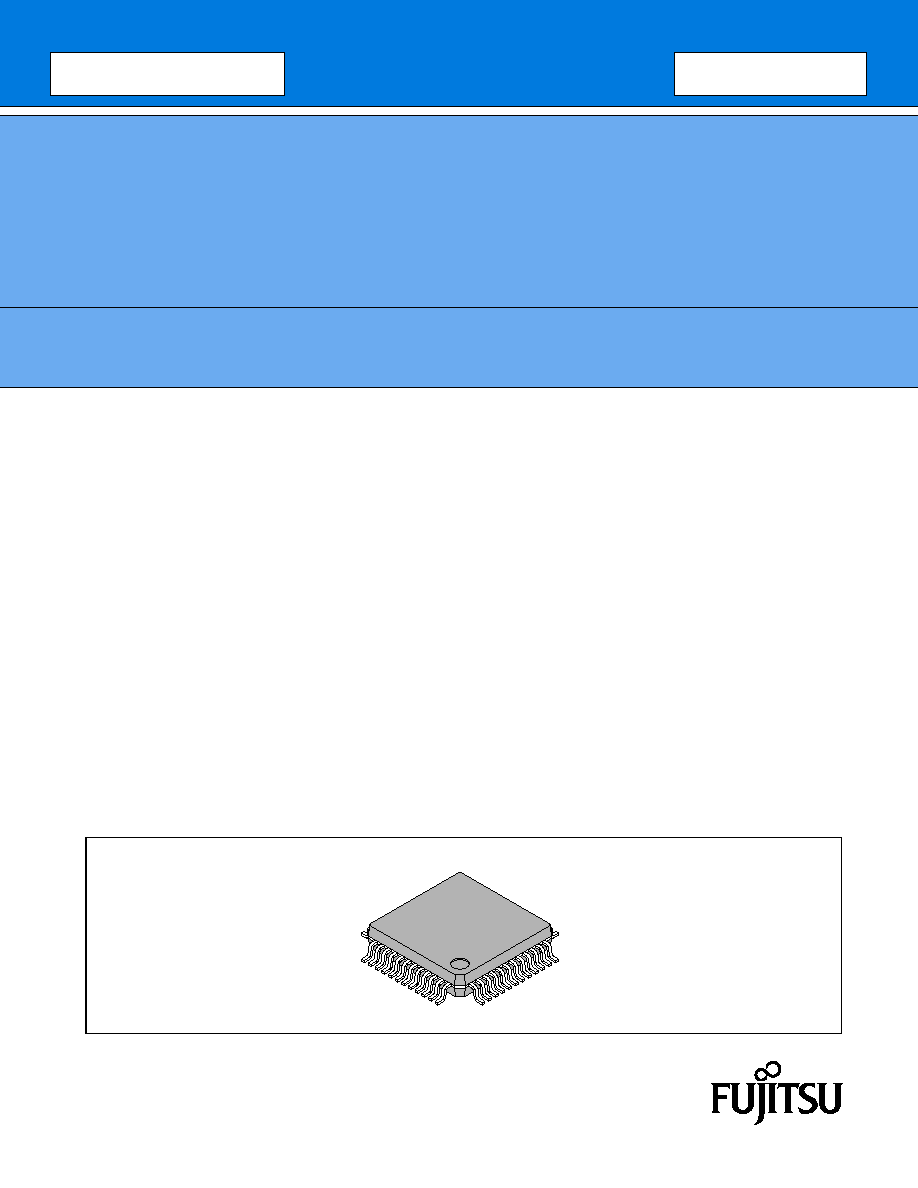
PACKAGE
48-pin plastic, LQFP
(FPT-48P-M26)

MB90895 Series
2
(Continued)
�
�
�
�
Instruction system best suited to controller
� Wide choice of data types (bit, byte, word, and long word)
� Wide choice of addressing modes (23 types)
� Enhanced multiply-divide instructions and RETI instructions
� Enhanced high-precision computing with 32-bit accumulator
�
�
�
�
Instruction system compatible with high-level language (C language) and multitask
� Employing system stack pointer
� Enhanced various pointer indirect instructions
� Barrel shift instructions
�
�
�
�
Increased processing speed
� 4-byte instruction queue
�
�
�
�
Powerful interrupt function with 8 levels and 34 factors
�
�
�
�
Automatic data transfer function independent of CPU
� Expanded intelligent I/O service function (EI
2
OS): Maximum of 16 channels
�
�
�
�
Low power consumption (standby) mode
� Sleep mode (a mode that halts CPU operating clock)
� Time-base timer mode (a mode that operates oscillation clock, sub clock, time-base timer and clock timer only)
� Clock mode (a mode that operates sub clock and clock timer only)
� Stop mode (a mode that stops oscillation clock and sub clock)
� CPU blocking operation mode
�
�
�
�
Process
� CMOS technology
�
�
�
�
I/O port
� General-purpose input/output port (CMOS output): 34 ports (MB90F897) (including 4 high-current output
ports) (When sub clock is not used, 36 ports (MB90F897S))
�
�
�
�
Timer
� Time-base timer, clock timer, watchdog timer: 1 channel
� 8/16-bit PPG timer: 8-bit x 4 channels, or 16-bit x 2 channels
� 16-bit reload timer: 2 channels
� 16-bit input/output timer
- 16-bit free run timer: 1 channel
- 16-bit input capture: (ICU): 4 channels
Interrupt request is issued upon latching a count value of 16-bit free run timer by detection of an edge on pin input.
�
�
�
�
CAN controller: 1 channel
� Compliant with Ver 2.0A and Ver 2.0B CAN specifications
� 8 built-in message buffers
� Transmission rate of 10 Kbps to 1 Mbps (by 16 MHz machine clock)
� CAN wake-up
�
�
�
�
UART0 (SCI), UART1(SCI): 2 channel
� Equipped with full-duplex double buffer
� Clock-asynchronous or clock-synchronous serial transmission is available.
�
�
�
�
DTP/External interrupt: 4 channels, CAN wake-up: 1channel
� Module for activation of expanded intelligent I/O service (EI
2
OS), and generation of external interrupt.
�
�
�
�
Delay interrupt generator module
� Generates interrupt request for task switching.
�
�
�
�
8/10-bit A/D converter: 8 channels
� Resolution is selectable between 8-bit and 10-bit.
� Activation by external trigger input is allowed.
� Conversion time: 6.125
�
s (at 16-MHz machine clock, including sampling time)
�
�
�
�
Program patch function
� Address matching detection for 2 address pointers.
MB90895 Series
3
s
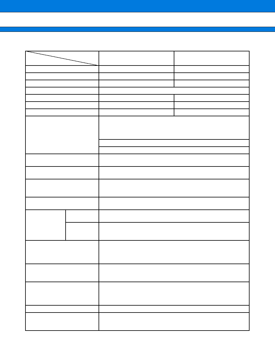
PRODUCT LINEUP
(Continued)
Part Number
MB90F897/S
MB90V495G
Parameter
Classification
Flash ROM
Evaluation product
ROM capacity
64 Kbytes
RAM capacity
2 Kbytes
6 Kbytes
Process
CMOS
Package
LQFP-48 (0.50 mm width)
PGA256
Operating power supply voltage
3.5 V to 5.5 V
4.5 V to 5.5 V
Special power supply for emulator*
1
None
CPU functions
Number of basic instructions
Instruction bit length
Instruction length
Data bit length
: 351 instructions
: 8 bits and 16 bits
: 1 byte to 7 bytes
: 1 bit, 8 bits, 16 bits
Minimum instruction execution time : 62.5 ns (at 16-MHz machine clock)
Interrupt processing time : 1.5
�
s at minimum (at 16-MHz machine clock)
Low power consumption
(standby) mode
Sleep mode/Clock mode/Time-base timer mode/
Stop mode/CPU intermittent
I/O port
General-purpose input/output ports (CMOS output) : 34 ports (36 ports*
2
)
including 4 high-current output ports (P14 to P17)
Time-base timer
18-bit free-run counter
Interrupt cycle : 1.024 ms, 4.096 ms, 16.834 ms, 131.072 ms
(with oscillation clock frequency at 4 MHz)
Watchdog timer
Reset generation cycle: 3.58 ms, 14.33 ms, 57.23 ms, 458.75 ms
(with oscillation clock frequency at 4 MHz)
16-bit input/output
timer
16-bit free-run
timer
Number of channels: 1
Interrupt upon occurrence of overflow
Input capture
Number of channels: 4
Retaining free-run timer value set by pin input (rising edge, falling edge, and
both edges)
16-bit reload timer
Number of channels: 2
16-bit reload timer operation
Count clock cycle: 0.25
�
s, 0.5
�
s, 2.0
�
s (at 16-MHz machine clock frequency)
External event count is allowed.
Clock timer
15-bit free-run counter
Interrupt cycle: 31.25 ms, 62.5 ms, 12 ms, 250 ms, 500 ms, 1.0 s, 2.0 s
(with 8.192 kHz sub clock)
8/16-bit PPG timer
Number of channels: 2 (four 8-bit channels are available also.)
PPG operation is allowed with four 8-bit channels or one 16-bit channel.
Outputting pulse wave of arbitrary cycle or arbitrary duty is allowed.
Count clock: 62.5 ns to 1
�
s (with 16 MHz machine clock)
Delay interrupt generator module
Interrupt generator module for task switching. Used for real-time OS.
DTP/External interrupt
Number of inputs: 4
Activated by rising edge, falling edge, "H" level or "L" level input.
External interrupt or expanded intelligent I/O service (EI
2
OS) is available.
MB90895 Series
4
(Continued)
*1 : Settings of DIP switch S2 for using emulation pod MB2145-507. For details, see MB2145-507 Hardware Manual
(2.7 Power Pin solely for Emulator).
*2 : MB90F897S
s
s
s
s
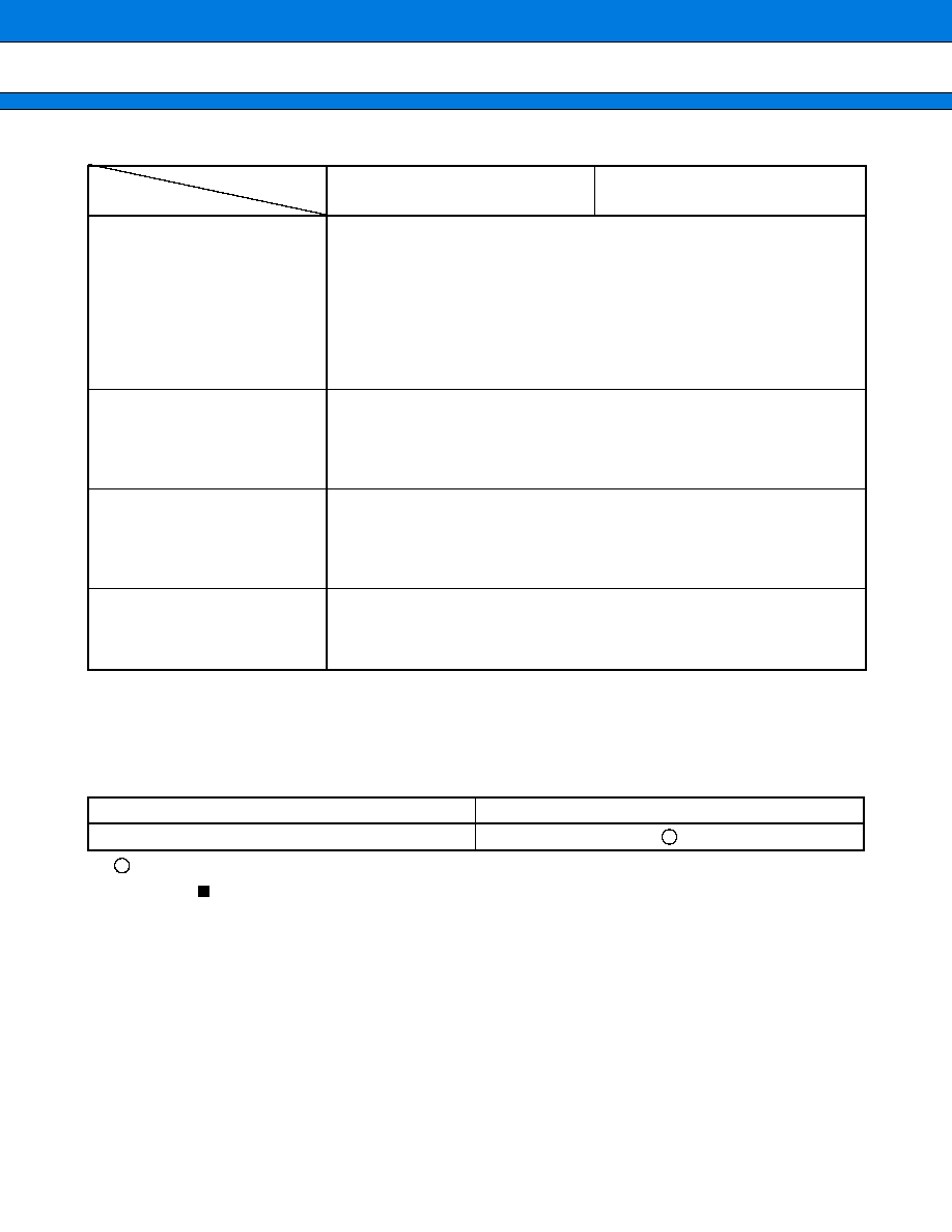
PACKAGES AND PRODUCT MODELS
: Yes,
�
: No
Note : Refer to " PACKAGE DIMENSION" for details of the package.
s
s
s
s
PRODUCT COMPARISON
Memory space
When testing with test product for evaluation, check the differences between the product and a product to be
used actually. Pay attention to the following points:
� The MB90V495G has no built-in ROM. However, a special-purpose development tool allows the operations
as those of one with built-in ROM. ROM capacity depends on settings on a development tool.
� On MB90V495G, an image from FF4000
H
to FFFFFF
H
is viewed on 00 bank and an image of FE0000
H
to
FF3FFF
H
is viewed only on FE bank and FF bank. (Modified on settings of a development tool.)
� On MB90F897/S, an image from FF4000
H
to FFFFFF
H
is viewed on 00 bank and an image of FF0000
H
to
FF3FFF
H
is viewed only on FF bank.
Part Number
MB90F897/S
MB90V495G
Parameter
8/10-bit A/D converter
Number of channels: 8
Resolution: Selectable 10-bit or 8-bit.
Conversion time: 6.125
�
s (at 16-MHz machine clock, including sampling time)
Sequential conversion of two or more successive channels is allowed. (Setting
a maximum of 8 channels is allowed.)
Single conversion mode
: Selected channel is converted only once.
Sequential conversion mode: Selected channel is converted repetitively.
Halt conversion mode
: Conversion of selected channel is stopped and
activated alternately.
UART0 (SCI)
Number of channels: 1
Clock-synchronous transfer: 62.5 Kbps to 2 Mbps
Clock-asynchronous transfer: 1,202 bps to 62,500 bps
Communication is allowed by bi-directional serial communication function and
master/slave type connection.
UART1 (SCI)
Number of channels: 1
Clock-synchronous transfer: 62.5 Kbps to 2 Mbps
Clock-asynchronous transfer: 9,615 bps to 500 Kbps
Communication is allowed by bi-directional serial communication function and
master/slave type connection.
CAN
Compliant with Ver 2.0A and Ver 2.0B CAN specifications.
8 built-in message buffers.
Transmission rate of 10 Kbps to 1 Mbps (by 16 MHz machine clock)
CAN wake-up
Package
MB90F897/S
FPT-48P-M26
MB90895 Series
5
s
s
s
s
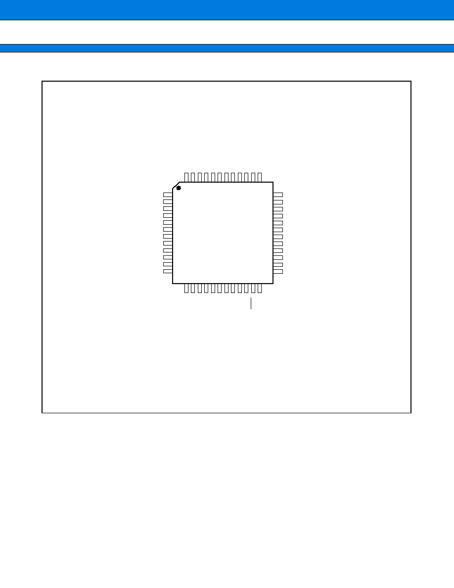
PIN ASSIGNMENT
1
2
3
4
5
6
7
8
9
10
11
12
AV
CC
AVR
P50/AN0
P51/AN1
P52/AN2
P53/AN3
P54/AN4
P55/AN5
P56/AN6
P57/AN7
P37/ADTG
P20/TIN0
36
35
34
33
32
31
30
29
28
27
26
25
P17/PPG3
P16/PPG2
P15/PPG1
P14/PPG0
P13/IN3
P12/IN2
P11/IN1
P10/IN0
X1
X0
C
V
SS
48
47
46
45
44
43
42
41
40
39
38
37
AV
SS
X1A/P36*
X0A/P35*
P33
P32/SIN0
P31SCK0
P30/SOT0
P44/RX
P43/TX
P42/SOT1
P41/SCK1
P40/SIN1
13
14
15
16
17
18
19
20
21
22
23
24
P21/TOT0
P22/TIN1
P23/TOT1
P24/INT4
P25/INT5
P26/INT6
P27/INT7
MD2
MD1
MD0
RST
V
CC
(FPT-48P-M26)
(TOP VIEW)
* : MB90F897
: X1A, X0A
MB90F897S
: P36, P35