 | –≠–ª–µ–∫—Ç—Ä–æ–Ω–Ω—ã–π –∫–æ–º–ø–æ–Ω–µ–Ω—Ç: MB90F949 | –°–∫–∞—á–∞—Ç—å:  PDF PDF  ZIP ZIP |
DS07-13741-2E
FUJITSU SEMICONDUCTOR
DATA SHEET
16-bit Proprietary Microcontroller
CMOS
F
2
MC-16LX MB90945 Series
MB90F946A/947A/F947/F947A/F949/F949A/
V390HA/V390HB
DESCRIPTION
The MB90945 series with one FULL-CAN* interface and FLASH ROM is especially designed for automotive HVAC
applications. Its main feature is the on board CAN* Interface, which conform to V2.0 Part A and Part B, while
supporting a very flexible message buffer scheme and so offering more functions than a normal FULL-CAN*
approach. With the new 0.35
µ
m CMOS technology, Fujitsu now offers on-chip FLASH-ROM program memory
up to 384 K bytes. An internal voltage booster removes the necessity for a second programming voltage.
An on board voltage regulator provides 3 V to the internal MCU core. This creates a major advantage in terms
of EMI and power consumption.
The internal PLL clock frequency multiplier provides an internal 42 ns instruction cycle time from an external
4 MHz clock.
The unit features a 4-channel Output Compare Unit and a 6-channel Input Capture Unit with two separate 16-bit
free running timers. Up to 3 UARTs, one Serial I/O and one I
2
C constitute additional functionality for communication
purposes.
* : Controller Area Network (CAN) - License of Robert Bosch GmbH
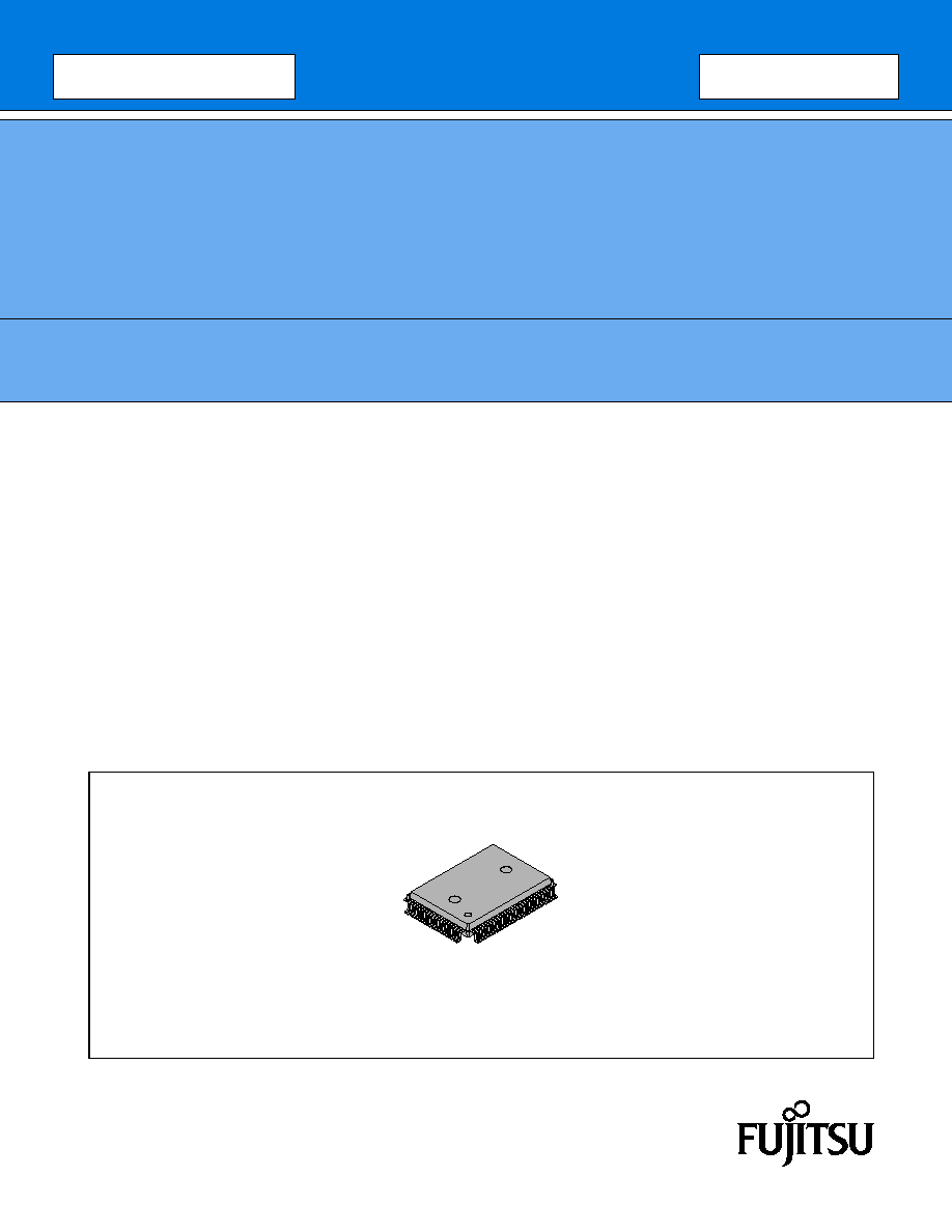
PACKAGE
100-pin Plastic QFP
(FPT-100P-M06)

MB90945 Series
2
FEATURES
∑ 16-bit core CPU; 4 MHz external clock (24 MHz internal, 42 ns instr. cycle time)
∑ New 0.35
µ
m CMOS Process Technology
∑ Internal voltage regulator supports 3 V MCU core, offering low EMI and low power consumption figures
∑ One FULL-CAN interface; conforming to Version 2.0 Part A and Part B, flexible message buffering (mailbox
and FIFO buffering can be mixed)
∑ Powerful interrupt functions (8 progr. priority levels; 8 external interrupts)
∑ EI
2
OS - Automatic transfer function independant of CPU; 16 channels of intelligent I/O Services
∑ 18-bit Time-base counter
∑ Watchdog Timer
∑ 1 full duplex UART; support 10.4 KBaud (USA standard)
∑ up to 2 full duplex UARTs (LIN/SCI/SPI)
∑ 1 Serial I/O (SPI)
∑ 1 I
2
C interface
∑ A/D Converter : 15 channels analog inputs (Resolution 10-bit or 8-bit)
∑ 16-bit reload timer
◊
1channel
∑ ICU (Input capture) 16-bit
◊
6 channels
∑ OCU (Output compare) 16-bit
◊
4 channels
∑ 16-bit free running timer
◊
2 channels (FRT0 : ICU 0/1, OCU 0/1/2/3, FRT1 : ICU 2/3/4/5)
∑ 8/16-bit Programmable Pulse Generator 6 channels
◊
8/16-bit
∑ Optimized instruction set for controller applications (bit, byte, word and long-word data types; 23 different
addressing modes; barrel shift; variety of pointers)
∑ 4-byte instruction execution queue
∑ signed multiply (16-bit
◊
16-bit) and divide (32-bit/16-bit) instructions available
∑ Program Patch Function (3 address match registers)
∑ Fast Interrupt processing
∑ Low Power Consumption mode
Sleep mode
Timebase timer mode
Stop mode
CPU intermittent mode
∑ Automotive input levels
∑ Package : 100-pin plastic QFP
MB90945 Series
3
PRODUCT LINEUP
(Continued)
Part Number
Parameter
MB90947A
MB90F946A
MB90F947, MB90F947A
MB90F949, MB90F949A
MB90V390HA
MB90V390HB
CPU
F
2
MC-16LX CPU
System clock
On-chip PLL clock multiplier (
◊
1,
◊
2,
◊
3,
◊
4,
◊
6, 1/2 when PLL stops)
Minimum instruction execution time : 42 ns (4 MHz oscillation clock, PLL clock
multiplied by 6)
ROM
ROM memory
128 Kbytes
Boot-block
Flash memory
384 Kbytes
Boot-block
Flash memory
256 Kbytes: MB90F949
MB90F949A
128 Kbytes: MB90F947
MB90F947A
External
RAM
6 Kbytes
16 Kbytes
12 Kbytes: MB90F949
MB90F949A
6 Kbytes: MB90F947
MB90F947A
30 Kbytes
Emulator-specific
power supply
*1
Yes
Technology
0.35
µ
m CMOS with
on-chip voltage
regulator for internal
power supply
0.35
µ
m CMOS with on-chip voltage regulator
for internal power supply
+
Flash memory
with on-chip charge pump for programming
voltage
0.35
µ
m CMOS with
on-chip voltage
regulator for internal
power supply
Operating
voltage range
3.5 V to 5.5 V : other than conditions listed below
4.0 V to 5.5 V : when writing to Flash
4.5 V to 5.5 V : if A/D Converter is used
5 V
±
10
%
Temperature range
-
40
∞
C to
+
105
∞
C
Package
QFP-100P
PGA-299C
UART
1 channel
2 channels
Full duplex double buffer
Supports asynchronous/synchronous (with start/stop bit) transfer
Baud rate : 4808/9615/10417/19230/38460/62500/500000 bps (asynchronous)
500 K/1 M/2 Mbps (synchronous) at System clock
=
20 MHz
UART
(LIN/SCI/SPI)
1 channel
2 channels
1 channel
2 channels
Serial I/O
1 channel
Transfer can be started from MSB or LSB
Supports internal clock synchronized transfer and external clock synchronized transfer
Supports positive-edge and negative-edge clock synchronization
Baud rate : 31.25 K/62.5 K/125 K/500 K/1 Mbps at System clock
=
20 MHz
I
2
C (400 Kbps)
1 channel
MB90945 Series
4
(Continued)
Part Number
Parameter
MB90947A
MB90F946A
MB90F947, MB90F947A
MB90F949, MB90F949A
MB90V390HA
MB90V390HB
A/D Converter
(15 input channels)
10-bit or 8-bit resolution
Conversion time : Min 4.9
µ
s includes sample time (per one channel, only at certain
machine clock frequencies)
16-bit Reload Timer
1 channel
2 channels
Operation clock frequency : fsys/2
1
, fsys/2
3
, fsys/2
5
(fsys
=
System clock frequency)
Supports External Event Count function
16-bit
I/O Timer
(2 channels)
Signals an interrupt when overflowing
Supports Timer Clear when a match with Output Compare (ch0)
Operation clock freq. : fsys, fsys/2
1
, fsys/2
2
, fsys/2
3
, fsys/2
4
, fsys/2
5
, fsys/2
6
, fsys/2
7
(fsys
=
System clock freq.)
I/O Timer 0 (clock input FRCK0) corresponds to ICU 0/1, OCU 0/1/2/3
I/O Timer 1 (clock input FRCK1) corresponds to ICU 2/3/4/5
16-bit
Input Capture
(6 channels)
Rising edge, falling edge or rising & falling edge sensitive
Six 16-bit Capture registers
Signals an interrupt upon external event
ICU 3/5 inputs are
shared with OCU 6/7
outputs
16-bit
Output Compare
4 channels
8 channels
Signals an interrupt when a match with 16-bit I/O Timer
Eight 16-bit compare registers.
A pair of compare registers can be used to generate an output signal.
ICU 3/5 inputs are
shared with OCU 6/7
outputs
8/16-bit
Programmable
Pulse Generator
(6 channels)
Supports 8-bit and 16-bit operation modes
Twelve 8-bit reload counters
Twelve 8-bit reload registers for L pulse width
Twelve 8-bit reload registers for H pulse width
A pair of 8-bit reload counters can be configured as one 16-bit reload counter or as
8-bit prescaler plus 8-bit reload counter
Operation clock freq. : fsys, fsys/2
1
, fsys/2
2
, fsys/2
3
, fsys/2
4
or 102.4
µ
s (fosc
=
5 MHz)
(fsys
=
System clock frequency, fosc
=
Oscillation clock frequency)
CAN Interface
1 channel
5 channels
Conforms to CAN Specification Version 2.0 Part A and B
Automatic re-transmission in case of error
Automatic transmission responding to Remote Frame
Prioritized 16 message buffers for data and ID's
Supports multiple messages
Flexible configuration of acceptance filtering :
Full-bit compare/Full-bit mask/Two partial bit masks
Supports up to 1 Mbps
MB90F947/F949/V390HA: Do not use clock modulation and CAN at the same time
MB90945 Series
5
(Continued)
Part Number
Parameter
MB90947A
MB90F946A
MB90F947, MB90F947A
MB90F949, MB90F949A
MB90V390HA
MB90V390HB
External Interrupt
(8 channels)
Can be programmed edge sensitive or level sensitive
Stepping motor
controller
2 channels
Watch Timer
1 channel
Sound generator
1 channel
Machine clock out-
put
2 channels
(non-inverted and in-
verted)
Program patch
function
3 address match registers
5 address match
registers
I/O Ports
Virtually all external pins can be used as general purpose I/O
All push-pull outputs
Bit-wise programmable as input/output or peripheral signal
Automotive input level (P21/RX1, P42/SDA, P43/SCL have CMOS
Schmitt input level)
Port-wise program-
mable as Automotive
(default) or CMOS
Schmitt input level
I/O Ports with 4 mA
CMOS output
All ports except P42, P43
All ports except P80,
P81, PA0 to PA7,
P42, P43
I/O Ports with 3 mA
CMOS output
P42, P43
P42, P43
I/O Ports with 30 mA
CMOS output with
slewrate control
P80, P81,
PA0 to PA7
Clock Modulator
Phase modulation mode
Phase modulation mode
Frequency and
phase
modulation mode
MB90F947/F949/V390HA:
Do not use clock modulation and CAN at the
same time
Reduces EMI by modulating the PLL clock
Start-up time at
power-on reset
3
◊
2
16
oscillation cycles (49.152 ms at 4 MHz oscillation)
+
oscilla-
tion time of oscillator*
2
2
18
oscillation cycles
(65.536 ms at 4 MHz
oscillation)
+
oscillation time of os-
cillator*
2