DS07-13502-5E
FUJITSU SEMICONDUCTOR
DATA SHEET
16-bit Proprietary Microcontroller
CMOS
F
2
MC-16F MB90220 Series
MB90223/224/P224A/W224A
MB90P224B/W224B/V220
s
OUTLINE
The MB90220 series of general-purpose high-performance 16-bit microcontrollers has been developed primarily
for applications that demand high-speed real-time processing and is suited for industrial applications, office
automation equipment, process control, and other applications. The F
2
MC-16F CPU is based on the F
2
MC*-16
Family with improved high-level language support functions and task switching functions, as well as additional
addressing modes.
On-chip peripheral resources include a 4-channel PWC timer, a 4-channel ICU (Input Capture Unit), a 1-channel
24-bit timer counter, an 8-channel OCU (Output Compare Unit), a 6-channel 16-bit reload timer, a 2-channel
16-bit PPG timer, a 10-bit A/D converter with 16 inputs, and a 4-channel serial port with a UART function (one
channel includes the CTS function).
The MB90P224B, MB90W224B, MB90224 is under development.
*: F
2
MC stands for FUJITSU Flexible Microcontroller.
s
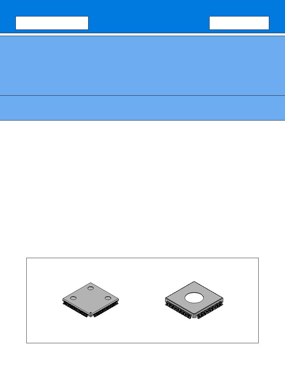
PACKAGE
120-pin Plastic QFP
(FPT-120P-M03)
120-pin Ceramic QFP
(FPT-120C-C02)

MB90220 Series
2
s
FEATURES
F
2
MC-16F CPU
∑ Minimum execution time: 62.5 ns/16 MHz oscillation (using a duty control system)
∑ Instruction sets optimized for controllers
Upward object-compatible with the F
2
MC-16(H)
Various data types (bit, byte, word, and long-word)
Instruction cycle improved to speed up operation
Extended addressing modes: 25 types
High coding efficiency
Access method (bank access with linear pointer)
Enhanced multiplication and division instructions (with signed instructions added)
Higher-precision operation using a 32-bit accumulator
∑ Extended intelligent I/O service (automatic transfer function independent of instructions)
Access area expanded to 64 Kbytes
∑ Enhanced instruction set applicable to high-level language (C) and multitasking
System stack pointer
Enhanced pointer-indirect instructions
Barrel shift instruction
Stack check function
∑ Increased execution speed: 8-byte instruction queue
∑ Powerful interrupt functions: 8 levels and 28 sources
Peripheral resources
∑ Mask ROM
: 64 Kbytes (MB90223)
96 Kbytes (MB90224)
EPROM
: 96 Kbytes (MB90W224A/W224B)
∑ One-time PROM : 96 Kbytes (MB90P224A/P224B)
∑ RAM: 3 Kbytes (MB90223)
4.5 Kbytes (MB90224/MB90W224A/P224A/W224B/P224B)
5 Kbytes (MB90V220)
∑ General-purpose ports: max. 102 channels
∑ ICU (Input Capture Unit): 4 channels
∑ 24-bit timer counter: 1 channel
∑ OCU (Output Compare Unit): 8 channels
∑ PWC timer with time measurement function: 4 channels
∑ 10-bit A/D converter: 16 channels
∑ UART: 4 channels (one channel includes CTS function)
∑ 16-bit reload timer
Toggled output, external clock, and gate functions: 6 channels
∑ 16-bit PPG timer: 2 channels
∑ DTP/External-interrupt inputs: 8 channels (of which five have edge detection function only)
∑ Write-inhibit RAM: 0.5 Kbytes (1 Kbyte for MB90V220)
∑ Timebase counter: 18 bits
∑ Clock gear function
∑ Low-power consumption mode
Sleep mode
Stop mode
Hardware standby mode
3
MB90220 Series
Product description
∑ MB90223/224 are mask ROM product.
∑ MB90P224A/P224B are one-time PROM products.
∑ MB90W224A/W224B are EPROM products. ES only.
∑ Operating temperature of MB90P224A/W224A is ≠40
∞
C to +85
∞
C.
(However, the AC characteristics is assured in ≠40
∞
C to +70
∞
C)
∑ Operation clock cycle of MB90223 is 10 MHz to 12 MHz.
∑ MB90V220 is a evaluation device for the program development. ES only.
s
PRODUCT LINEUP
(Continued)
MB90223
MB90224
MB90P224A
MB90P224B
MB90W224A
MB90W224B
MB90V220
Classification
Mask ROM
product
Mask ROM
product
One-time
PROM product
EPROM
product
Evaluation
device
ROM size
64 Kbytes
96 Kbytes
96 Kbytes
96 Kbytes
None
RAM size
3 Kbytes
4.5 Kbytes
4.5 Kbytes
4.5 Kbytes
5 Kbytes
CPU functions
The number of instructions:
412
Instruction bit length:
8 or 16 bits
Instruction length:
1 to 7 bytes
Data bit length:
1, 4, 8, 16, or 32 bits
Minimum execution time:
62.5 ns/16 MHz
Interrupt processing time:
1.0
µ
s/16 MHz (min.)
Ports
I/O ports (N-ch open-drain):
16
I/O ports (CMOS):
86
Total:
102
ICU
(Input Capture Unit)
Number of channels: 4
Rising edge/falling edge/both edges selectable
24-bit timer
counter
Number of channels: 1
Overflow interrupt, intermediate bit interrupt
OCU
(Output Compare Unit)
Number of channels: 8
Pin change source (match signal causes register value transfer/general-purpose port)
PWC timer
Number of channels: 4
16-bit reload timer operation (operation clock cycle: 0.25
µ
s to 1.31 ms)
16-bit pulse-width count operation (Allowing continuous/one-shot measurement, H/L width
measurement, inter-edge measurement, and divided-frequency measurement)
10-bit
A/D converter
Resolution: 10 bits
Number of inputs: 16
Single conversion mode (conversion of each channel)
Scan conversion mode (continuous conversion for up to 16 consecutive channels)
Continuous conversion mode (repeated conversion of specified channel)
Stop conversion mode (conversion every fixed cycle)
UART
Number of channels: 4 (1 channel with CTS function)
Clock-synchronous transfer mode
(full-duplex double buffering, 7 to 9-bit data length, 2400 to 62500 bps)
Asynchronous transfer mode
(full-duplex double buffering, 7 to 9-bit data length, 2400 to 62500 bps)
16-bit reload
timer
Number of channels: 6
16-bit reload timer operation (operation clock cycle: 0.25
µ
s to 1.05 s)
Part number
Item
MB90220 Series
4
(Continued)
Note: MB90V220 is a evaluation device, therefore, the electrical characteristics are not assured.
s
DIFFERENCES BETWEEN MB90223/224 (MASK ROM PRODUCT) AND MB90P224A/
W224A/P224B/W224B
MB90223
MB90224
MB90P224A
MB90P224B
MB90W224A
MB90W224B
MB90V220
16-bit PPG timer
Number of channels: 2
16-bit PPG operation (operation clock cycle: 0.25
µ
s to 6 s)
DTP/External
interrupts
Number of inputs: 8 (of which five have edge detection function only)
External interrupt mode (allowing interrupts to activate at four different request levels)
Simple DMA transfer mode (allowing extended I
2
OS to activate at two different request levels)
Write-inhibited
RAM
RAM size: 512 bytes (1 Kbyte for MB90V220)
RAM write-protectable with WI pin
Standby mode
stop mode (activated by software or hardware) and sleep mode
Gear function
Machine clock operation frequency switching: 16 MHz, 8 MHz, 4 MHz, 1 MHz (at
16-MHz oscillation)
Package
FPT-120P-M03
FPT-120C-C02
PGA-256C-A02
MB90223
MB90224
MB90P224A
MB90P224B
MB90W224A
MB90W224B
ROM
Mask ROM
64 Kbytes
Mask ROM
96 Kbytes
OTPROM
96 Kbytes
EPROM
96 Kbytes
Pin functions: pin 87
MD2 pin
MD2/V
PP
pin
Part number
Item
Part number
Item
5
MB90220 Series
s
PIN ASSIGNMENT
P01/D01 96
P02/D02 97
P03/D03 98
P04/D04 99
P05/D05 100
P06/D06 101
P07/D07 102
P10/D08 103
P11/D09 104
P12/D10 105
P13/D11 106
P14/D12 107
P15/D13 108
P16/D14 109
P17/D15 110
P20/A00 111
P21/A01 112
P22/A02 113
P23/A03 114
P24/A04 115
P25/A05 116
P26/A06 117
P27/A07 118
V
SS
119
P30/A08 120
60 PA5/INT0
59 PA4/PWC3/POT3/ASR3
58 PA3/PWC2/POT2/ASR2
57 PA2/PWC1/POT1/ASR1
56 PA1/PWC0/POT0
55 PA0/ASR0
54 V
CC
53 P67/AN07
52 P66/AN06
51 P65/AN05
50 P64/AN04
49 P63/AN03
48 P62/AN02
47 P61/AN01
46 P60/AN00
45 AV
SS
44 AVRL
43 AVRH
42 AV
CC
41 P97/AN15
40 P96/AN14
39 P95/AN13
38 P94/AN12
37 P93/AN11
36 P92/AN10
35 P91/AN09
34 P90/AN08
33 V
SS
32 P87/PPG1
31 P86/PPG0
V
SS
91
X0 92
X1 93
V
CC
94
P00/D00 95
P31/A09 1
P32/A10 2
P33/A11 3
P34/A12 4
P35/A13 5
P36/A14 6
P37/A15 7
V
CC
8
P40/A16 9
P41/A17 10
P42/A18 11
P43/A19/TIN1/INT3 12
P44/A20/TIN2/INT4 13
P45/A21/TIN3/INT5 14
P46/A22/TIN4/INT6 15
P47/A23/TIN5/INT7 16
P70/DOT0 17
P71/DOT1 18
P72/DOT2 19
P73/DOT3 20
P74/DOT4 21
P75/DOT5 22
P76/DOT6 23
P77/DOT7 24
P80/TOT0 25
P81/TOT1 26
P82/TOT2 27
P83/TOT3 28
P84/TOT4 29
P85/TOT5 30
90 RST
89 MD0
88 MD1
87 MD2
86 HST
85 P57/WI
84 P56/RD
83 P55/WRL
82 P54/WRH
81 P53/HRQ
80 P52/HAK
79 P51/RDY
78 P50/CLK
77 PC5/TRG0
76 PC4/CTS0
75 PC3/SCK3
74 PC2/SID3
73 PC1/SOD3
72 PC0/SCK2
71 PB7/SID2
70 PB6/SOD2
69 PB5/SCK1
68 PB4/SID1
67 PB3/SOD1
66 PB2/SCK0
65 PB1/SID0
64 PB0/SOD0
63 V
SS
62 PA7/INT2/ATG
61 PA6/INT1
(Top view)
(FPT-120P-M03)
(FPT-120C-C02)
MB90220 Series
6
s
PIN DESCRIPTION
* : FPT-120P-M03, FPT-120C-C02
(Continued)
Pin no.
Pin name
Circuit
type
Function
QFP*
92,
93
X0,
X1
A
Crystal oscillation pins (16 MHz)
89 to 87
MD0 to MD2
D
Operation mode specification input pins
Connect directly to V
CC
or V
SS
.
90
RST
G
External reset request input
86
HST
E
Hardware standby input pin
95 to 102
P00 to P07
C
General-purpose I/O ports
This function is valid only in single-chip mode.
D00 to D07
Output pins for low-order 8 bits of the external address bus.
This function is valid only in modes where the external bus is
enabled.
103 to 110
P10 to P17
C
General-purpose I/O ports
This function is valid only in single-chip mode or when the external bus
is enabled and the 8-bit data bus specification has been made.
D08 to D15
I/O pins for higher-order 8 bits of the external data bus
This function is valid only when the external bus is enabled and the
16-bit bus specification has been made.
111 to 118
P20 to P27
C
General-purpose I/O ports
This function is valid only in single-chip mode.
A00 to A07
Output pins for lower-order 8 bits of the external address bus
This function is valid only in modes where the external bus is
enabled.
120,
1 to 7
P30,
P31 to P37
C
General-purpose I/O ports
This function is valid either in single-chip mode or when the address
mid-order control register specification is "port".
A08,
A09 to A15
Output pins for mid-order 8 bits of the external address bus
This function is valid in modes where the external bus is enabled and
the address mid-order control register specification is "address".
9 to 11
P40 to P42
C
General-purpose I/O ports
This function is valid either in single-chip mode or when the address
high-order control register specification is "port".
A16 to A18
Output pins for higher-order 8 bits of the external address bus
This function is valid in modes where the external bus is enabled and
the address high-order control register specification is "address".
12 to 16
P43 to P47
C
General-purpose I/O ports
This function is valid when either single-chip mode is enabled or the
address higher-order control register specification is "port".
A19 to A23
Output pins for higher-order 8 bits of the external address bus
This function is valid in modes where the external bus is enabled and
the address higher-order control register specification is "address".
TIN1 to TIN5
16-bit reload timer input pins
This function is valid when the timer input specification is "enabled".
The data on the pins is read as timer input (TIN1 to TIN5).
7
MB90220 Series
* : FPT-120P-M03, FPT-120C-C02
(Continued)
Pin no.
Pin name
Circuit
type
Function
QFP*
12 to 16
INT3 to INT7
C
External interrupt request input pins
When external interrupts are enabled, these inputs may be used
suddenly at any time; therefore, it is necessary to stop output by other
functions on these pins, except when using them for output
deliberately.
78
P50
C
General-purpose I/O port
This function is valid in single-chip mode and when the CLK output
specification is disabled.
CLK
CLK output pin
This function is valid in modes where the external bus is enabled and
the CLK output specification is enabled.
79
P51
C
General-purpose I/O port
This function is valid in single-chip mode or when the ready function
is disabled.
RDY
Ready input pin
This function is valid in modes where the external bus is enabled and
the ready function is enabled.
80
P52
C
General-purpose I/O port
This function is valid in single-chip mode or when the hold function is
disabled.
HAK
Hold acknowledge output pin
This function is valid in modes where the external bus is enabled and
the hold function is enabled.
81
P53
C
General-purpose I/O port
This function is valid in single-chip mode or external bus mode and
when the hold function is disabled.
HRQ
Hold request input pin
This function is valid in modes where the external bus is enabled and
the hold function is enabled.
During this operation, the input may be used suddenly at any time;
therefore, it is necessary to stop output by other fuctions on this pin,
except when using it for output deliberately.
82
P54
C
General-purpose I/O port
This function is valid in single-chip mode, when the external bus is in
8-bit mode, or when WRH pin output is disabled.
WRH
Write strobe output pin for the high-order 8 bits of the data bus
This function is valid in modes where the external bus is enabled, the
external bus is in 16-bit mode, and WRH pin output is enabled.
83
P55
C
General-purpose I/O port
This function is valid in single-chip mode or when WRL pin output is
disabled.
WRL
Write strobe output pin for the low-order 8 bits of the data bus
This function is valid in modes where the external bus is enabled and
WRL pin output is enabled.
MB90220 Series
8
* : FPT-120P-M03, FPT-120C-C02
(Continued)
Pin no.
Pin name
Circuit
type
Function
QFP*
84
P56
C
General-purpose I/O port
This function is valid in single-chip mode. This function is valid in
modes where the external bus is valid.
RD
Read strobe output pin for the data bus
This function is valid in modes where the external bus is enabled.
85
P57
B
General-purpose I/O port
This function is always valid.
When these pins are open in input mode, through current may leak in
stop mode/reset mode, be sure to fix these pins to V
CC
/V
SS
level to
use these pins in input mode.
WI
RAM write disable request input
During this operation, the input may be used suddenly at any time;
therefore, it is necessary to stop output by other fuctions on this pin,
except when using it for output deliberately.
46 to 53
P60 to P67
F
Open-drain I/O ports
This function is valid when the analog input enable register
specification is "port".
AN00 to AN07
10-bit A/D converter analog input pins
This function is valid when the analog input enable register
specification is "analog input".
17 to 24
P70 to P77
C
General-purpose I/O ports
This function is valid when the output specification for DOT0 to DOT7
is "disabled".
DOT0 to DOT7
This function is valid when OCU (output compare unit) output is
enabled.
25 to 30
P80 to P85
C
General-purpose I/O ports
This function is valid when the output specification for TOT0 to TOT5
is "disabled".
TOT0 to TOT5
16-bit reload timer output pins (TOT0 to TOT5)
31,
32
P86,
P87
C
General-purpose I/O ports
This function is valid when the PPG0, and PPG1 output specification
is "disabled".
PPG0,
PPG1
16-bit PPG timer output pins
This function is valid when the PPG control/status register
specification is "PPG output pins".
34 to 41
P90 to P97
F
Open-drain I/O ports
This function is valid when the analog input enable register
specification is "port".
AN08 to AN15
10-bit A/D converter analog input pins
This function is valid when the analog input enable register
specification is "analog input".
9
MB90220 Series
* : FPT-120P-M03, FPT-120C-C02
(Continued)
Pin no.
Pin name
Circuit
type
Function
QFP*
55
PA0
C
General-purpose I/O port
This function is always valid.
ASR0
ICU (input capture unit) input pin
This function is valid during ICU (input capture unit) input operations.
56
PA1
C
General-purpose I/O port
This function is always valid.
PWC0
PWC input pin
During PWC0 input operations, this input may be used suddenly at
any time; therefore, it is necessary to stop output by other functions
on this pin, except when using it for output deliberately.
POT0
PWC output pin
This function is valid during PWC output operations.
57 to 59
PA2 to PA4
C
General-purpose I/O ports
This function is always valid.
PWC1 to PWC3
PWC input pins
This function is valid during PWC input operations.
During PWC1 to PWC3 input operations, this input may be used
suddenly at any time; therefore, it is necessary to stop output by other
functions on this pin, except when using it for output deliberately.
POT1 to POT3
PWC output pins
This function is valid during PWC output operations.
ASR1 to ASR3
ICU (input capture unit) input pins
This function is valid during ICU (input capture unit) input operations.
60,
61
PA5,
PA6
B
General-purpose I/O ports
This function is always valid.
When these pins are open in input mode, through current may leak in
stop mode/reset mode, be sure to fix these pins to V
CC
/V
SS
level to
use these pins in input mode.
INT0,
INT1
DTP/External interrupt request input pins
When DTP/external interrupts are enabled, these inputs may be used
suddenly at any time; therefore, it is necessary to stop output by other
functions on these pins, except when using them for output
deliberately.
When these pins are open in input mode, through current may leak in
stop mode/reset mode, be sure to fix these pins to V
CC
/V
SS
level to
use these pins in input mode.
62
PA7
B
General-purpose I/O port
This function is always valid.
When these pins are open in input mode, through current may leak in
stop mode/reset mode, be sure to fix these pins to V
CC
/V
SS
level to
use these pins in input mode.
MB90220 Series
10
* : FPT-120P-M03, FPT-120C-C02
(Continued)
Pin no.
Pin name
Circuit
type
Function
QFP*
62
INT2
B
DTP/External interrupt request input pin
When DTP/external interrupts are enabled, these inputs may be used
suddenly at any time; therefore, it is necessary to stop output by other
functions on these pins, except when using them for output
deliberately.
When these pins are open in input mode, through current may leak in
stop mode/reset mode, be sure to fix these pins to V
CC
/V
SS
level to
use these pins in input mode.
ATG
10-bit A/D converter external trigger input pin
When these pins are open in input mode, through current may leak in
stop mode/reset mode, be sure to fix these pins to V
CC
/V
SS
level to
use these pins in input mode.
64
PB0
C
General-purpose I/O port
This function is valid when the UART0 (ch.0) serial data output
specification is "disabled".
SOD0
UART0 (ch.0) serial data output
This function is valid when the UART0 (ch.0) serial data output
specification is "enabled".
65
PB1
C
General-purpose I/O port
This function is always valid.
SID0
UART0 (ch.0) serial data input pin
During UART0 (ch.0) input operations, this input may be used
suddenly at any time; therefore, it is necessary to stop output by other
functions on this pin, except when using it for output deliberately.
66
PB2
C
General-purpose output port
This function is valid when the UART0 (ch.0) clock output
specification is "disabled".
SCK0
UART0 (ch.0) clock output pin
The clock output function is valid when the UART0 (ch.0) clock output
specification is "enabled".
UART0 (ch.0) external clock input pin. This function is valid when the
port is in input mode and the UART0 (ch.0) specification is external
clock mode.
67
PB3
C
General-purpose I/O port
This function is valid when the UART0 (ch.1) serial data output
specification is "disabled".
SOD1
UART0 (ch.1) serial data output pin
This function is valid when the UART0 (ch.1) serial data output
specification is "enabled".
68
PB4
C
General-purpose I/O port
This function is always valid.
SID1
UART0 (ch.1) serial data input pin
During UART0 (ch.1) input operations, this input may be used
suddenly at any time; therefore, it is necessary to stop output by other
functions on this pin, except when using it for output deliberately.
11
MB90220 Series
* : FPT-120P-M03, FPT-120C-C02
(Continued)
Pin no.
Pin name
Circuit
type
Function
QFP*
69
PB5
C
General-purpose I/O port
This function is valid when the UART0 (ch.1) clock output specification
is "disabled".
SCK1
UART0 (ch.1) clock output pin
The clock output function is valid when the UART0 (ch.1) clock output
specification is "enabled".
UART0 (ch.1) external clock input pin
This function is valid when the port is in input mode and the UART0
(ch.1) specification is external clock mode.
70
PB6
C
General-purpose I/O port
This function is valid when the UART0 (ch.2) serial data output
specification is "disabled".
SOD2
UART0 (ch.2) serial data output pin
This function is valid when the UART0 (ch.2) serial data output
specification is "enabled".
71
PB7
C
General-purpose I/O port
This function is always valid.
SID2
UART0 (ch.2) serial data input pin
During UART0 (ch.2) input operations, this input may be used
suddenly at any time; therefore, it is necessary to stop output by other
functions on this pin, except when using it for output deliberately.
72
PC0
C
General-purpose I/O port
This function is valid when the UART0 (ch.2) clock output
specification is "disabled".
SCK2
UART0 (ch.2) clock output pin
The clock output function is valid when the UART0 (ch.2) clock output
specification is "enabled".
UART0 (ch.2) external clock input pin
This function is valid when the port is in input mode and the UART0
(ch.2) specification is external clock mode.
73
PC1
C
General-purpose I/O port
This function is valid when the UART1 serial data output specification
is "disabled".
SOD3
UART1 serial data output pin
This function is valid when the UART1 serial data output specification
is "enabled".
74
PC2
C
General-purpose I/O port
This function is always valid.
SID3
UART1 serial data input pin
During UART1 input operations, this input may be used suddenly at
any time; therefore, it is necessary to stop output by other functions
on this pin, except when using it for output deliberately.
MB90220 Series
12
(Continued)
* : FPT-120P-M03, FPT-120C-C02
(Continued)
Pin no.
Pin name
Circuit
type
Function
QFP*
75
PC3
C
General-purpose I/O port
This function is valid when the UART1 clock output specification is
"disabled".
SCK3
UART1 clock output pin
The clock output function is valid when the UART1 clock output
specification is "enabled".
UART1 external clock input pin
This function is valid when the port is in input mode and the UART1
specification is external clock mode.
76
PC4
C
General-purpose I/O port
This function is always valid.
CTS0
UART0 (ch.0) Clear To Send input pin
When the UART0 (ch.0) CTS function is enabled, this input may be
used suddenly at any time; therefore, it is necessary to stop output by
other functions on this pin, except when using it for output
deliberately.
77
PC5
C
General-purpose I/O port
This function is always valid.
TRG0
16-bit PPG timer trigger input pin
This function is valid when the 16-bit PPG timer trigger input
specification is enabled.
The data on this pin is read as 16-bit PPG timer trigger input (TRG0).
During this operation, the input may be used suddenly at any time;
therefore, it is necessary to stop output by other functions on this pin,
except when using it for output deliberately.
8,
54,
94
V
CC
Power
supply
Power supply for digital circuitry
33,
63,
91,
119
V
SS
Power
supply
Ground level for digital circuitry
42
AV
CC
Power
supply
Power supply for analog circuitry
When turning this power supply on or off, always be sure to first apply
electric potential equal to or greater than AV
CC
to V
CC
.
During normal operation AV
CC
should be equal to V
CC
.
43
AVRH
Power
supply
Reference voltage input for analog circuitry
When turning this pin on or off, always be sure to first apply electric
potential equal to or greater than AVRH to AV
CC
.
44
AVRL
Power
supply
Reference voltage input for analog circuitry
45
AV
SS
Power
supply
Ground level for analog circuitry
13
MB90220 Series
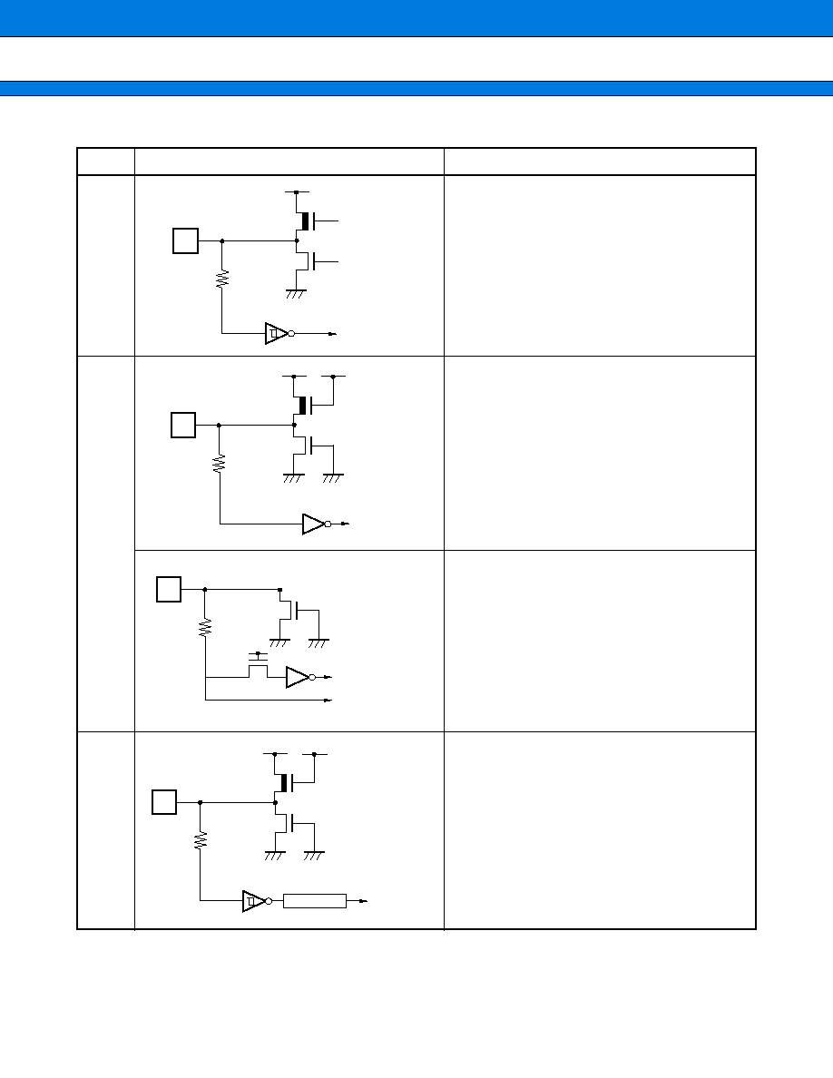
s
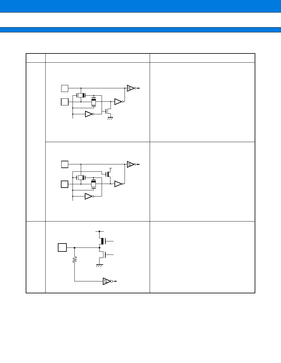
I/O CIRCUIT TYPE
Note: The pull-up and pull-down resistors are always connected, regardless of the state.
(Continued)
Type
Circuit
Remarks
A
∑ Oscillation feedback resistor: Approx. 1 M
MB90223
MB90224
MB90P224B
MB90W224B
∑ Oscillation feedback resistor: Approx. 1 M
MB90P224A
MB90W224A
B
∑ CMOS-level output
∑ CMOS-level hysteresis input with no standby
control
X1
X0
Standby control signal
X1
X0
Standby control signal
Digital output
Digital output
Digital input
R
MB90220 Series
14
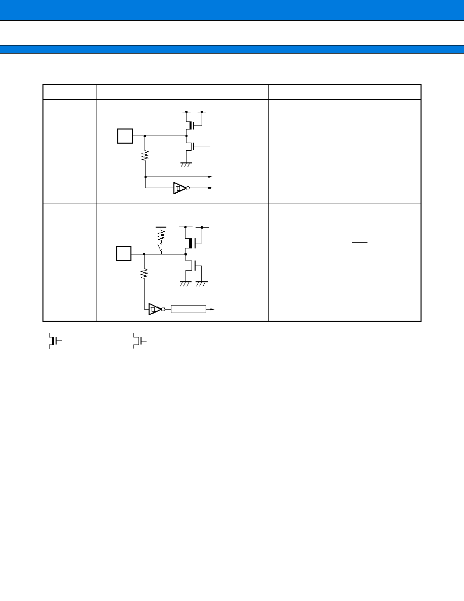
Note: The pull-up and pull-down resistors are always connected, regardless of the state.
(Continued)
Type
Circuit
Remarks
C
∑ CMOS-level output
∑ CMOS-level hysteresis input with standby
control
D
∑ CMOS-level input with no standby control
Mask ROM products only:
MD2: with pull-down resistor
MD1: with pull-up resistor
MD0: with pull-down resistor
∑ CMOS-level input with no standby control
MD2 of OTPROM products/EPROM products
only
E
∑ CMOS-level hysteresis input with no standby
control
∑ With input analog filter (40 ns Typ.)
Digital output
Digital output
Digital input
R
Digital input
R
VPP power supply
Digital input
R
Digital input
R
Analog filter
15
MB90220 Series
(Continued)
Note: The pull-up and pull-down resistors are always connected, regardless of the state.
Type
Circuit
Remarks
F
∑ N-channel open-drain output
∑ CMOS-level hysteresis input with A/D
control and with standby control
G
∑ CMOS-level hysteresis input with no
standby control and with pull-up resistor
∑ With input analog filter (40 ns Typ.)
MB90223, MB90224: RST pin can be set
to with or without a pull-up resistor by a
mask option.
MB90P224A: With pull-up resistor
MB90W224A: With pull-up resistor
MB90P224B: With no pull-up resistor
MB90W224B: With no pull-up resistor
Digital output
A/D input
R
Digital input
Digital input
R
R
Analog filter
Pull-up
resistor
: P-type transistor
: N-type transistor
MB90220 Series
16
s
HANDLING DEVICES
1. Preventing Latchup
CMOS ICs may cause latchup when a voltage higher than V
CC
or lower than V
SS
is applied to input or output
pins other than medium-and high-voltage pins, or when a voltage exceeding the rating is applied between V
CC
and V
SS
.
If latch-up occurs, the power supply current increases rapidly, sometimes resulting in thermal breakdown of the
device. Use meticulous care not to let any voltage exceed the maximum rating.
Also, take care to prevent the analog power supply (AV
CC
and AVRH) and analog input from exceeding the
digital power supply (V
CC
) when the analog system power supply is turned on and off.
2. Treatment of Unused Input Pins
Leaving unused input pins open could cause malfunctions. They should be connected to a pull-up or pull-down
resistor.
3. Treatment of Pins when A/D is not Used
Connect to be AV
CC
= AVRH = V
CC
and AV
SS
= AVRL = V
SS
even if the A/D converter is not in use.
4. Precautions when Using an External Input
To reset the internal circuit properly by the "L" level input to the RST pin, the "L" level input to the RST pin must
be maintained for at least five machine cycles. Pay attention to it if the chip uses external clock input.
5. V
CC
and V
SS
Pins
Apply equal potential to the V
CC
and V
SS
pins.
6. Supply Voltage Variation
The operation assurance range for the V
CC
supply voltage is as given in the ratings. However, sudden changes
in the supply voltage can cause misoperation, even if the voltage remains within the rated range. Therefore, it
is important to supply a stable voltage to the IC. The recommended power supply control guidelines are that
the commercial frequency (50 to 60 Hz) ripple variation (P-P value) on V
CC
should be less than 10% of the
standard V
CC
value and that the transient rate of change during sudden changes, such as during power supply
switching, should be less than 0.1 V/ms.
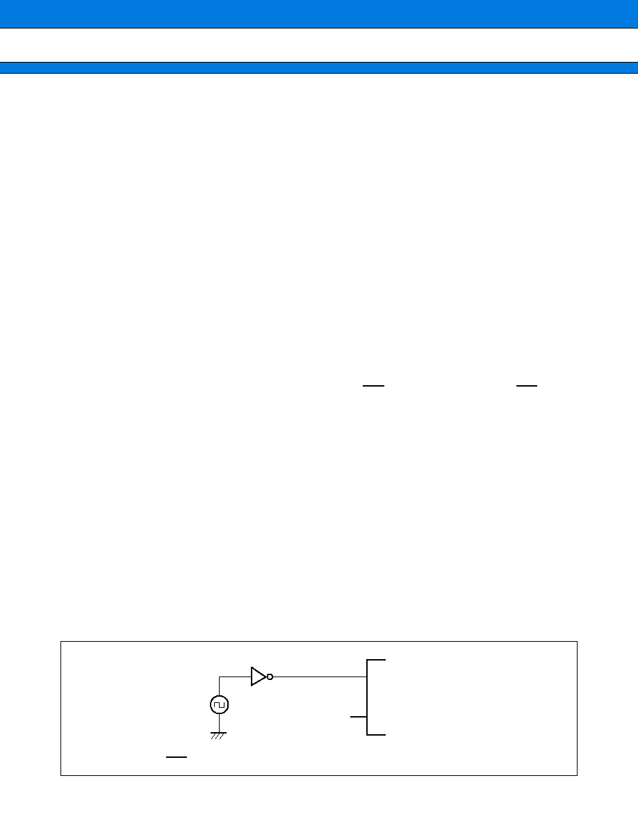
7. Notes on Using an External Clock
When using an external clock, drive the X0 pin as illustrated below. When an external clock is used, oscillation
stabilization time is required even for power-on reset and wake-up from stop mode.
∑
Use of External Clock
X0
X1
MB90220
Note: When using an external clock, be sure to input external clock more than 6 machine cycles after
setting the HST pin to "L" to transfer to the hardware standby mode.

17
MB90220 Series
8. Power-on Sequence for A/D Converter Power Supplies and Analog Inputs
Be sure to turn on the digital power supply (V
CC
) before applying voltage to the A/D converter power supplies
(AV
CC
, AVRH, and AVRL) and analog inputs (AN00 to AN15).
When turning power supplies off, turn off the A/D converter power supplies (AV
CC
, AVRH, and AVRL) and analog
inputs (AN00 to AN15) first, then the digital power supply (V
CC
).
When turning AVRH on or off, be careful not to let it exceed AV
CC
.
MB90220 Series
18
s
PROGRAMMING FOR MB90P224A/P224B/W224A/W224B
In EPROM mode, the MB90P224A/P224B/W224A/W224B functions equivalent to the MBM27C1000. This
allows the EPROM to be programmed with a general-purpose EPROM programmer by using the dedicated
socket adapter (do not use the electronic signature mode).
1. Program Mode
When shipped from Fujitsu, and after each erasure, all bits (96 K
◊
8 bits) in the MB90P224A/P224B/W224A/
W224B are in the "1" state. Data is written to the ROM by selectively programming "0's" into the desired bit
locations. Bits cannot be set to "1" electrically.
2. Programming Procedure
(1) Set the EPROM programmer to MBM27C1000.
(2) Load program data into the EPROM programmer at 08000
H
to 1FFFF
H
.
Note that ROM addresses FE8000
H
to FFFFFF
H
in the operation mode in the MB90P224A/P224B/W224A/
W224B series assign to 08000
H
to 1FFFF
H
in the EPROM mode (on the EPROM programmer).
(3) Mount the MB90P224A/P224B/W224A/W224B on the adapter socket, then fit the adapter socket onto the
EPROM programmer. When mounting the device and the adapter socket, pay attention to their mounting
orientations.
(4) Start programming the program data to the device.
(5) If programming has not successfully resulted, connect a capacitor of approx. 0.1
µ
F between V
CC
and GND,
between V
PP
and GND.
Note: The mask ROM products (MB90223, MB90224) does not support EPROM mode. Data cannot, therefore, be
read by the EPROM programmer.
FFFFFF
H
08000
H
*
1FFFF
H
*
Operation mode
* : Be sure to set the programming, the start address and the stop address on the EPROM programmer to 08000
H
/1FFFF
H
.
EPROM mode
(Corresponding addresses on the EPROM mode)
FE8000
H

19
MB90220 Series
3. EPROM Programmer Socket Adapter and Recommended Programmer Manufacturer
Inquiry: Sun Hayato Co., Ltd.: TEL: (81)-3-3986-0403
FAX: (81)-3-5396-9106
Advantest Corp.:
TEL: Except JAPAN (81)-3-3930-4111
4. Erase Procedure
Data written in the MB90W224A/W224B is erased (from "0" to "1") by exposing the chip to ultraviolet rays with
a wavelength of 2,537 ≈ through the translucent cover.
Recommended irradiation dosage for exposure is 10 Wsec/cm
2
. This amount is reached in 15 to 20 minutes
with a commercial ultraviolet lamp positioned 2 to 3 cm above the package (when the package surface illuminance
is 1200
µ
W/cm
2
).
If the ultraviolet lamp has a filter, remove the filter before exposure. Attaching a mirrored plate to the lamp
increases the illuminance by a factor of 1.4 to 1.8, thus shortening the required erasure time. If the translucent
part of the package is stained with oil or adhesive, transmission of ultraviolet rays is degraded, resulting in a
longer erasure time. In that case, clean the translucent part using alcohol (or other solvent not affecting the
package).
The above recommended dosage is a value which takes the guard band into consideration and is a multiple of
the time in which all bits can be evaluated to have been erased. Observe the recommended dosage for erasure;
the purpose of the guard band is to ensure erasure in all temperature and supply voltage ranges. In addition,
check the life span of the lamp and control the illuminance appropriately.
Data in the MB90W224A/W224B is erased by exposure to light with a wavelength of 4,000 ≈ or less.
Data in the device is also erased even by exposure to fluorescent lamp light or sunlight although the exposure
results in a much lower erasure rate than exposure to 2,537 ≈ ultraviolet rays. Note that exposure to such lights
for an extended period will therefore affect system reliability. If the chip is used where it is exposed to any light
with a wavelength of 4,000 ≈ or less, cover the translucent part, for example, with a protective seal to prevent
the chip from being exposed to the light.
Exposure to light with a wavelength of 4,000 to 5,000 ≈ or more will not erase data in the device. If the light
applied to the chip has a very high illuminance, however, the device may cause malfunction in the circuit for
reasons of general semiconductor characteristics. Although the circuit will recover normal operation when
exposure is stopped, the device requires proper countermeasures for use in a place exposed continuously to
such light even though the wavelength is 4,000 ≈ or more.
Part No.
MB90P224B
Package
QFP-120
Compatible socket adapter
Sun Hayato Co., Ltd.
ROM-120QF-32DP-16F
Recommended
programmer
manufacturer
and
programmer
name
Advantest corp.
R4945A
(main unit)
+
R49451A
(adapter)
Recommended
MB90220 Series
20
5. Recommended Screening Conditions
High temperature aging is recommended as the pre-assembly screening procedure.
6. Programming Yeild
MB90P224A/P224B cannot be write-tested for all bits due to their nature. Therefore the write yield cannot always
be guaranteed to be 100%.
7. Pin Assignments in EPROM Mode
(1) Pins Compatible with MBM27C1000
MBM27C1000
MB90P224A/P224B/
MB90W224A/W224B
MBM27C1000
MB90P224A/P224B/
MB90W224A/W224B
Pin no.
Pin name
Pin no.
Pin name
Pin no.
Pin name
Pin no.
Pin name
1
V
PP
87
MD2 (V
PP
)
32
V
CC
8, 54, 94
V
CC
2
OE
83
P55
31
PGM
84
P56
3
A15
7
P37
30
N.C.
--
--
4
A12
4
P34
29
A14
6
P36
5
A07
118
P27
28
A13
5
P35
6
A06
117
P26
27
A08
120
P30
7
A05
116
P25
26
A09
1
P31
8
A04
115
P24
25
A11
3
P33
9
A03
114
P23
24
A16
9
P40
10
A02
113
P22
23
A10
2
P32
11
A01
112
P21
22
CE
82
P54
12
A00
111
P20
21
D07
102
P07
13
D00
95
P00
20
D06
101
P06
14
D01
96
P01
19
D05
100
P05
15
D02
97
P02
18
D04
99
P04
16
GND
33, 63, 91,119
V
SS
17
D03
98
P03
Program, verify
Aging
+150
∞
C, 48 Hrs.
Data verification
Assembly
21
MB90220 Series
(2) Power Supply and GND Connection Pins
(3) Pins other than MBM27C1000-compatible Pins
Type
Pin no.
Pin name
Power supply
89
88
86
8, 54, 94
MD0
MD1
HST
V
CC
GND
33, 63, 91, 119
44
45
80
81
90
V
SS
AVRL
AV
SS
P52
P53
RST
Pin no.
Pin name
Treatment
92
X0
Pull up with 4.7 K
resistor
93
X1
OPEN
109
110
10 to 16
42
43
46
47
48 to 53
17 to 24
25 to 32
34 to 41
55 to 61
63 to 70
71 to 76
78
79
85
103 to 108
P16
P17
P41 to P47
AV
CC
AVRH
P60
P61
P62 to P67
P70 to P77
P80 to P82
P90 to P97
PA0 to PA7
PB0 to PB7
PC0 to PC5
P50
P51
P57
P10 to P15
Connect pull-up resistor of about 1 M
to each pin
MB90220 Series
22
s
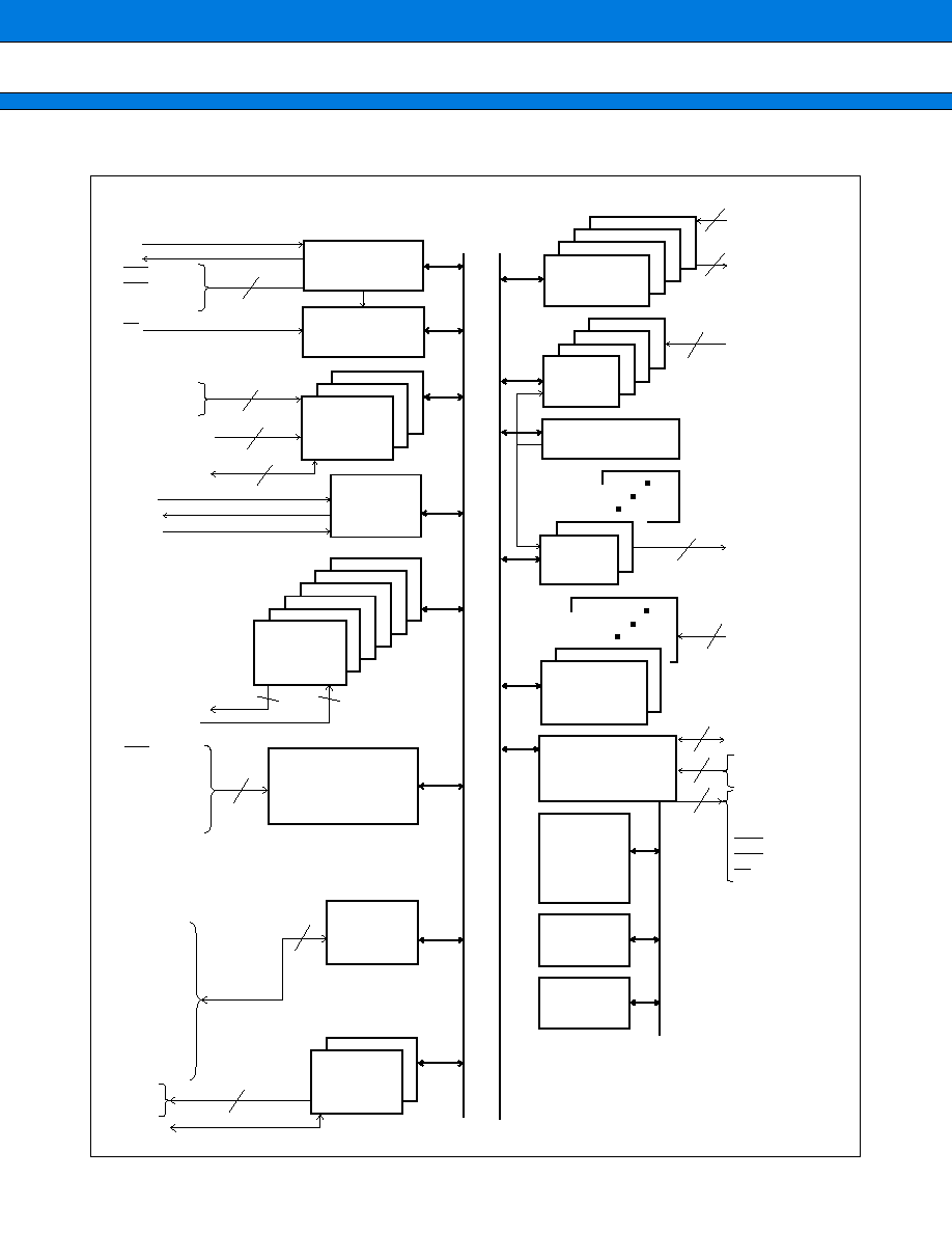
BLOCK DIAGRAM
Clock controller
5
X1
X0
RST
HST
MD0 to MD2
4
3
3
CTS0
SID0 to SID2
SCK0 to SCK2
SOD0 to SOD2
SID3
SOD3
SCK3
TOT0 to TOT5
TIN1 to TIN5
6
5
21
ATG
AN00 to AN15
AV
CC
AVRH
AVRL
AV
SS
102
P00 to P07
P10 to P17
P20 to P27
P30 to P37
P40 to P47
P50 to P57
P60 to P67
P70 to P77
P80 to P87
P90 to P97
PA0 to PA7
PB0 to PB7
PC0 to PC5
PPG0
PPG1
TRG0
2
4
4
PWC0 to PWC3
POT0 to POT3
UART0
◊
3
UART1
10-bit
A/D converter
16 channels
16-bit reload timer
◊
6
I/O ports
16-bit PPG timer
◊
2
ROM
RAM
F
2
MC-16F CPU
External bus
interface
DTP/External
interrupt
◊
8
24-bit timer counter
ICU (Input
Capture Unit)
◊
4
OCU (Output
Compare Unit)
◊
4
PWC timer
◊
4
4
8
DOT0 to DOT7
ASR0 to ASR3
INT0 to INT7
D00 to D15
RDY
HRQ
A00 to A23
CLK
HAK
WRH
WRL
RD
8
Internal data bus
16
2
29
WI
Write-inhibit
RAM
23
MB90220 Series
s
PROGRAMMING MODEL
Accumulator
User stack pointer
System stack pointer
Processor status
Program counter
User stack upper register
System stack upper register
User stack lower register
System stack lower register
Direct page register
Program bank register
Data bank register
User stack bank register
System stack bank register
Additional bank register
Max.32 banks
RW 7
RW 6
RW 5
RW 4
R 7
R 5
R 3
R 1
R 6
R 4
R 2
R 0
RW3
RW 2
RW 1
RW 0
RL 3
RL 2
RL 1
RL 0
000180
H
+ RP
◊
10
H
ILM
-- I S T N Z V C
Processor Status (PS)
General-purpose Registers
Dedicated Registers
AH
AL
USP
SSP
PS
PC
USPCU
SSPCU
USPCL
SSPCL
DPR
PCB
DTB
USB
SSB
ADB
8 bit
16 bit
32 bit
C C R
16 bit
RP
Lower
Upper
MSB LSB
MB90220 Series
24
s
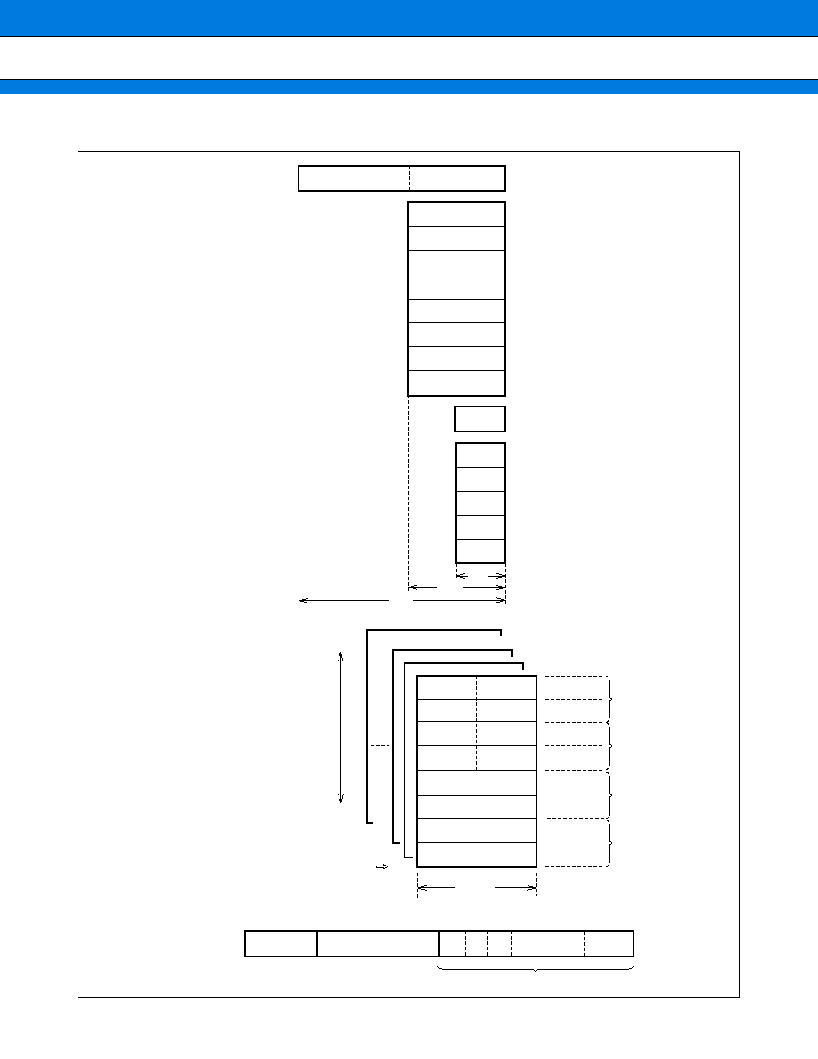
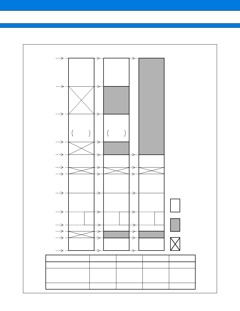
MEMORY MAP
Single chip
ROM area
ROM area
ROM area
FF bank
image
ROM area
FF bank
image
Internal
register area
Internal
register area
Write-inhibit
RAM
Write-inhibit
RAM
RAM
Registers
Registers
RAM
Peripherals
Peripherals
Peripherals
Internal
register area
Write-inhibit
RAM
Registers
RAM
: Internal
: External
: No access
FFFFFF
H
Address #1
010000
H
Address #2
002000
H
001F00
H
Address #3
Address #4
000380
H
000100
H
0000C0
H
000180
H
Internal ROM
and external bus
External ROM
and external bus
000000
H
Type
Address #1
Address #2
Address #3
Address #4
MB90223
MB90224
MB90P224A/P224B
MB90W224A/W224B
MB90V220
(FE0000
H
)
FF0000
H
FE8000
H
004000
H
004000
H
004000
H
001900
H
000F00
H
001500
H
001500
H
000D00
H
001300
H
25
MB90220 Series
s
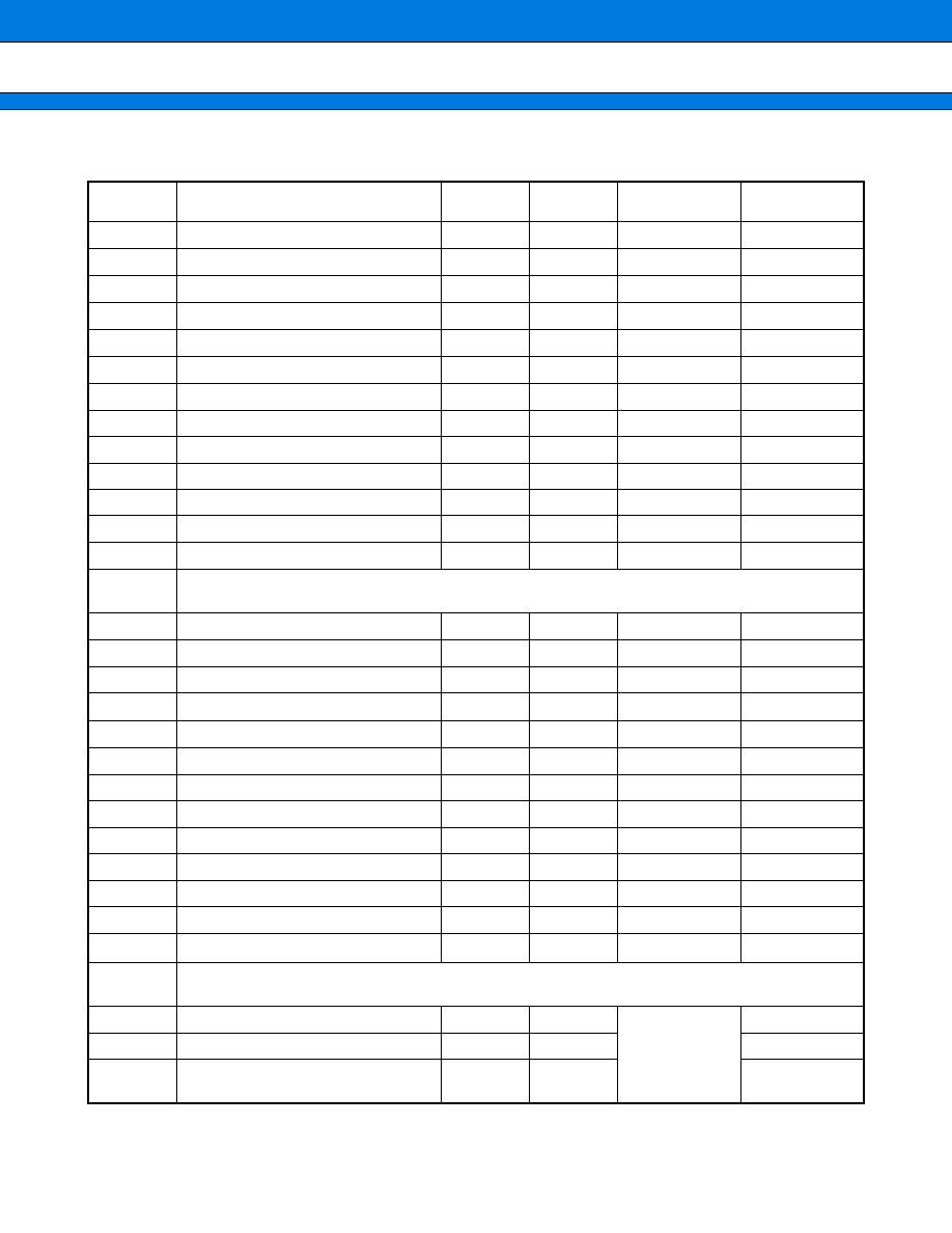
I/O MAP
(Continued)
Address
Register
Register
name
Access
Resouce
name
Initial value
000000
H
*3
Port 0 data register
PDR0
R/W
Port 0
X X X X X X X X
000001
H
*3
Port 1 data register
PDR1
R/W
Port 1
X X X X X X X X
000002
H
*3
Port 2 data register
PDR2
R/W
Port 2
X X X X X X X X
000003
H
*3
Port 3 data register
PDR3
R/W
Port 3
X X X X X X X X
000004
H
*3
Port 4 data register
PDR4
R/W
Port 4
X X X X X X X X
000005
H
*3
Port 5 data register
PDR5
R/W
Port 5
X X X X X X X X
000006
H
Port 6 data register
PDR6
R/W
Port 6
1 1 1 1 1 1 1 1
000007
H
Port 7 data register
PDR7
R
Port 7
X X X X X X X X
000008
H
Port 8 data register
PDR8
R/W
Port 8
X X X X X X X X
000009
H
Port 9 data register
PDR9
R/W
Port 9
1 1 1 1 1 1 1 1
00000A
H
Port A data register
PDRA
R/W
Port A
X X X X X X X X
00000B
H
Port B data register
PDRB
R/W
Port B
X X X X X X X X
00000C
H
Port C data register
PDRC
R/W
Port C
≠ ≠ X X X X X X
00000D
H
to 0F
H
(Reserved area)
*1
000010
H
*3
Port 0 data direction register
DDR0
R/W
Port 0
0 0 0 0 0 0 0 0
000011
H
*3
Port 1 data direction register
DDR1
R/W
Port 1
0 0 0 0 0 0 0 0
000012
H
*3
Port 2 data direction register
DDR2
R/W
Port 2
0 0 0 0 0 0 0 0
000013
H
*3
Port 3 data direction register
DDR3
R/W
Port 3
0 0 0 0 0 0 0 0
000014
H
*3
Port 4 data direction register
DDR4
R/W
Port 4
0 0 0 0 0 0 0 0
000015
H
*3
Port 5 data direction register
DDR5
R/W
Port 5
0 0 0 0 0 0 0 0
000016
H
Port 6 analog input enable register
ADER0
R/W
Port 6
1 1 1 1 1 1 1 1
000017
H
Port 7 data direction register
DDR7
R/W
Port 7
1 1 1 1 1 1 1 1
000018
H
Port 8 data direction register
DDR8
R/W
Port 8
0 0 0 0 0 0 0 0
000019
H
Port 9 analog input enable register
ADER1
R/W
Port 9
1 1 1 1 1 1 1 1
00001A
H
Port A data direction register
DDRA
R/W
Port A
0 0 0 0 0 0 0 0
00001B
H
Port B data direction register
DDRB
R/W
Port B
0 0 0 0 0 0 0 0
00001C
H
Port C data direction register
DDRC
R/W
Port C
≠ ≠
0 0 0 0 0 0
00001D
H
to 1F
H
(Reserved area)
*1
000020
H
Mode control register 0
UMC0
R/W
UART 0 (ch.0)
0 0 0 0 0 1 0 0
000021
H
Status register 0
USR0
R/W
0 0 0 1 0 0 0 0
000022
H
Input data register 0
/output data register 0
UIDR0
/UODR0
R/W
X X X X X X X X
MB90220 Series
26
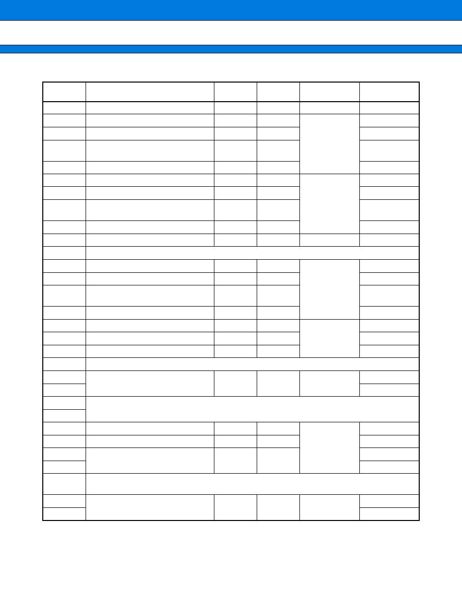
(Continued)
Address
Register
Register
name
Access
Resouce
name
Initial value
000023
H
Rate and data register 0
URD0
R/W
UART0 (ch.0)
0 0 0 0 0 0 0 X
000024
H
Mode control register 1
UMC1
R/W
UART0 (ch.1)
0 0 0 0 0 1 0 0
000025
H
Status register 1
USR1
R/W
0 0 0 1 0 0 0 0
000026
H
Input data register 1
/output data register 1
UIDR1
/UODR1
R/W
X X X X X X X X
000027
H
Rate and data register 1
URD1
R/W
0 0 0 0 0 0 0 X
000028
H
Mode control register 2
UMC2
R/W
UART0 (ch.2)
0 0 0 0 0 1 0 0
000029
H
Status register 2
USR2
R/W
0 0 0 1 0 0 0 0
00002A
H
Input data register 2
/output data register 2
UIDR2
/UODR2
R/W
X X X X X X X X
00002B
H
Rate and data register 2
URD2
R/W
0 0 0 0 0 0 0 X
00002C
H
UART CTS control register
UCCR
R/W
UART0 (ch.0)
≠ ≠ ≠ 0 0 0 ≠ ≠
00002D
H
(Reserved area)
*1
00002E
H
Mode register
SMR
R/W
UART1
0 0 0 0 0 0 0 0
00002F
H
Control register
SCR
R/W
0 0 0 0 0 1 0 0
000030
H
Input data register
/output data register
SIDR
/SODR
R/W
X X X X X X X X
000031
H
Status register
SSR
R/W
0 0 0 0 1 ≠ 0 0
000032
H
A/D channel setting register
ADCH
R/W
10-bit A/D
converter
0 0 0 0 0 0 0 0
000033
H
A/D mode register
ADMD
R/W
≠ ≠ ≠ X 0 0 0 0
000034
H
A/D control status register
ADCS
R/W
0 0 0 0 ≠ ≠ 0 0
000035
H
(Reserved area)
*1
000036
H
A/D data register
ADCD
R
10-bit A/D
converter
X X X X X X X X
000037
H
0 0 0 0 0 0 X X
000038
H
(Reserved area)
*1
000039
H
00003A
H
DTP/interrupt enable register
ENIR
R/W
DTP/external
interrupt
0 0 0 0 0 0 0 0
00003B
H
DTP/interrupt source register
EIRR
R/W
0 0 0 0 0 0 0 0
00003C
H
Request level setting register
ELVR
R/W
0 0 0 0 0 0 0 0
00003D
H
0 0 0 0 0 0 0 0
00003E
H
to 3F
H
(Reserved area)
*1
000040
H
Timer control status register 0
TMCSR0
R/W
16-bit reload
timer 0
0 0 0 0 0 0 0 0
000041
H
≠ ≠ ≠ ≠ 0 0 0 0
27
MB90220 Series
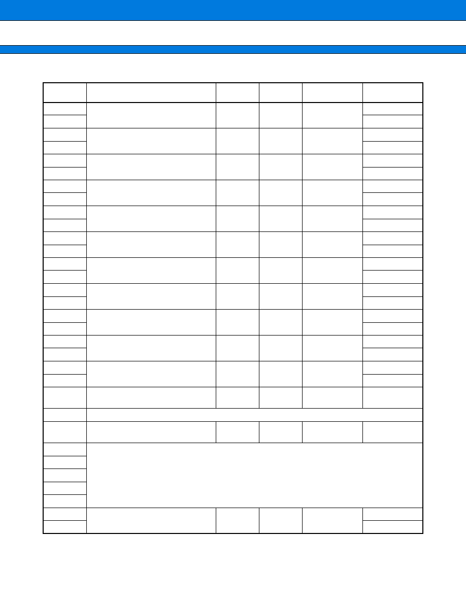
(Continued)
Address
Register
Register
name
Access
Resouce
name
Initial value
000042
H
Timer control status register 1
TMCSR1
R/W
16-bit reload
timer 1
0 0 0 0 0 0 0 0
000043
H
≠ ≠ ≠ ≠ 0 0 0 0
000044
H
Timer control status register 2
TMCSR2
R/W
16-bit reload
timer 2
0 0 0 0 0 0 0 0
000045
H
≠ ≠ ≠ ≠ 0 0 0 0
000046
H
Timer control status register 3
TMCSR3
R/W
16-bit reload
timer 3
0 0 0 0 0 0 0 0
000047
H
≠ ≠ ≠ ≠ 0 0 0 0
000048
H
Timer control status register 4
TMCSR4
R/W
16-bit reload
timer 4
0 0 0 0 0 0 0 0
000049
H
≠ ≠ ≠ ≠ 0 0 0 0
00004A
H
Timer control status register 5
TMCSR5
R/W
16-bit reload
timer 5
0 0 0 0 0 0 0 0
00004B
H
≠ ≠ ≠ ≠ 0 0 0 0
00004C
H
PPG control status register 0
PCNT0
R/W
16-bit PPG
timer 0
0 0 0 0 0 0 0 0
00004D
H
0 0 0 0 0 0 0 0
00004E
H
PPG control status register 1
PCNT1
R/W
16-bit PPG
timer 1
0 0 0 0 0 0 0 0
00004F
H
0 0 0 0 0 0 0 0
000050
H
PWC control status register 0
PWCSR0
R/W
PWC timer 0
0 0 0 0 0 0 0 0
000051
H
0 0 0 0 0 0 0 0
000052
H
PWC control status register 1
PWCSR1
R/W
PWC timer 1
0 0 0 0 0 0 0 0
000053
H
0 0 0 0 0 0 0 0
000054
H
PWC control status register 2
PWCSR2
R/W
PWC timer 2
0 0 0 0 0 0 0 0
000055
H
0 0 0 0 0 0 0 0
000056
H
PWC control status register 3
PWCSR3
R/W
PWC timer 3
0 0 0 0 0 0 0 0
000057
H
0 0 0 0 0 0 0 0
000058
H
ICU control register 0
ICC0
R/W
ICU (Input
Capture Unit)
0 0 0 0 0 0 0 0
000059
H
(Reserved area)
*1
00005A
H
Input capture control register 1
ICC1
R/W
ICU (Input
Capture Unit)
0 0 0 0 0 0 0 0
00005B
H
(Reserved area)
*1
00005C
H
00005D
H
00005E
H
00005F
H
000060
H
OCU control register 00
CCR00
R/W
OCU (Output
Compare Unit)
1 1 1 1 0 0 0 0
000061
H
≠ ≠ ≠ ≠ 0 0 0 0
MB90220 Series
28
(Continued)
Address
Register
Register
name
Access
Resouce
name
Initial value
000062
H
OCU0 control register 01
CCR01
R/W
OCU (Output
Compare Unit)
1 1 1 1 0 0 0 0
000063
H
≠ ≠ ≠ ≠ 0 0 0 0
000064
H
(Reserved area)
*1
000065
H
000066
H
000067
H
000068
H
OCU0 control register 10
CCR10
R/W
OCU (Output
Compare Unit)
≠ ≠ ≠ ≠ 0 0 0 0
000069
H
0 0 0 0 0 0 0 0
00006A
H
OCU0 control register 11
CCR11
R/W
≠ ≠ ≠ ≠ 0 0 0 0
00006B
H
0 0 0 0 0 0 0 0
00006C
H
(Reserved area)
*1
00006D
H
00006E
H
00006F
H
000070
H
Free-run timer control register
TCCR
R/W
24-bit timer
counter
1 1 0 0 0 0 0 0
000071
H
≠ ≠ 1 1 1 1 1 1
000072
H
Free-run timer lower-order data
register
TCRL
R
0 0 0 0 0 0 0 0
000073
H
0 0 0 0 0 0 0 0
000074
H
Free-run timer upper-order data
register
TCRH
0 0 0 0 0 0 0 0
000075
H
0 0 0 0 0 0 0 0
000076
H
(Reserved area)
*1
000077
H
000078
H
000079
H
00007A
H
PWC divider ratio control register 0
DIVR0
R/W
PWC timer 0
≠ ≠ ≠ ≠ ≠ ≠ 0 0
00007B
H
Reserved area
*1
00007C
H
PWC divider ratio control register 1
DIVR1
R/W
PWC timer 1
≠ ≠ ≠ ≠ ≠ ≠ 0 0
00007D
H
Reserved area
*1
00007E
H
PWC divider ratio control register 2
DIVR2
R/W
PWC timer 2
≠ ≠ ≠ ≠ ≠ ≠ 0 0
00007F
H
Reserved area
*1
000080
H
PWC divider ratio control register 3
DIVR3
R/W
PWC timer 3
≠ ≠ ≠ ≠ ≠ ≠ 0 0
000081
H
to 8D
H
(Reserved area)
*1
29
MB90220 Series
(Continued)
Address
Register
Register
name
Access
Resouce
name
Initial value
00008E
H
WI control register
WICR
R/W
Write-inhibit
RAM
≠ ≠ ≠ X ≠ ≠ ≠ ≠
00008F
H
(Reserved area)
*1
000090
H
to 9E
H
00009F
H
Delay interrupt source generation
/release register
DIRR
R/W
Delay interrupt
generation
module
≠ ≠ ≠ ≠ ≠ ≠ ≠ 0
0000A0
H
Standby control register
STBYC
R/W
Low power
consumption
0 0 0 1 * * * *
0000A3
H
Address mid-order control register
MACR
W
External pin
# # # # # # # #
0000A4
H
Address higher-order control
register
HACR
W
External pin
# # # # # # # #
0000A5
H
External pin control register
EPCR
W
External pin
# # 0 ≠ 0 # 0 0
0000A8
H
Watchdog timer control register
WDTC
R/W
Watchdog
timer
X X X X X X X X
0000A9
H
Timebase timer control register
TBTC
R/W
Timebase
timer
≠ ≠ ≠ 0 0 0 0 0
0000B0
H
Interrupt control register 00
ICR00
R/W
Interrupt
controller
0 0 0 0 0 1 1 1
0000B1
H
Interrupt control register 01
ICR01
R/W
0 0 0 0 0 1 1 1
0000B2
H
Interrupt control register 02
ICR02
R/W
0 0 0 0 0 1 1 1
0000B3
H
Interrupt control register 03
ICR03
R/W
0 0 0 0 0 1 1 1
0000B4
H
Interrupt control register 04
ICR04
R/W
0 0 0 0 0 1 1 1
0000B5
H
Interrupt control register 05
ICR05
R/W
0 0 0 0 0 1 1 1
0000B6
H
Interrupt control register 06
ICR06
R/W
0 0 0 0 0 1 1 1
0000B7
H
Interrupt control register 07
ICR07
R/W
0 0 0 0 0 1 1 1
0000B8
H
Interrupt control register 08
ICR08
R/W
0 0 0 0 0 1 1 1
0000B9
H
Interrupt control register 09
ICR09
R/W
0 0 0 0 0 1 1 1
0000BA
H
Interrupt control register 10
ICR10
R/W
0 0 0 0 0 1 1 1
0000BB
H
Interrupt control register 11
ICR11
R/W
0 0 0 0 0 1 1 1
0000BC
H
Interrupt control register 12
ICR12
R/W
0 0 0 0 0 1 1 1
0000BD
H
Interrupt control register 13
ICR13
R/W
0 0 0 0 0 1 1 1
0000BE
H
Interrupt control register 14
ICR14
R/W
0 0 0 0 0 1 1 1
0000BF
H
Interrupt control register 15
ICR15
R/W
0 0 0 0 0 1 1 1
0000C0
H
to FF
H
(External area)
*2
001F00
H
PWC data buffer register 0
PWCR0
R/W
PWC timer 0
0 0 0 0 0 0 0 0
001F01
H
0 0 0 0 0 0 0 0
MB90220 Series
30
(Continued)
Address
Register
Register
name
Access
Resouce
name
Initial value
001F02
H
PWC data buffer register 1
PWCR1
R/W
PWC timer 1
0 0 0 0 0 0 0 0
001F03
H
0 0 0 0 0 0 0 0
001F04
H
PWC data buffer register 2
PWCR2
R/W
PWC timer 2
0 0 0 0 0 0 0 0
001F05
H
0 0 0 0 0 0 0 0
001F06
H
PWC data buffer register 3
PWCR3
R/W
PWC timer 3
0 0 0 0 0 0 0 0
001F07
H
0 0 0 0 0 0 0 0
001F08
H
to 1F0F
H
(Reserved area)
*1
001F10
H
OCU compare lower-order data
register 00
CPR00L
R/W
Output
compare 00
0 0 0 0 0 0 0 0
001F11
H
0 0 0 0 0 0 0 0
001F12
H
OCU compare higher-order data
register 00
CPR00
0 0 0 0 0 0 0 0
001F13
H
0 0 0 0 0 0 0 0
001F14
H
OCU compare lower-order data
register 01
CPR01L
R/W
Output
compare 01
0 0 0 0 0 0 0 0
001F15
H
0 0 0 0 0 0 0 0
001F16
H
OCU compare higher-order data
register 01
CPR01
0 0 0 0 0 0 0 0
001F17
H
0 0 0 0 0 0 0 0
001F18
H
OCU compare lower-order data
register 02
CPR02L
R/W
Output
compare 02
0 0 0 0 0 0 0 0
001F19
H
0 0 0 0 0 0 0 0
001F1A
H
OCU compare higher-order data
register 02
CPR02
0 0 0 0 0 0 0 0
001F1B
H
0 0 0 0 0 0 0 0
001F1C
H
OCU compare lower-order data
register 03
CPR03L
R/W
Output
compare 03
0 0 0 0 0 0 0 0
001F1D
H
0 0 0 0 0 0 0 0
001F1E
H
OCU compare higher-order data
register 03
CPR03
0 0 0 0 0 0 0 0
001F1F
H
0 0 0 0 0 0 0 0
001F20
H
OCU compare lower-order data
register 04
CPR04L
R/W
Output
compare 10
0 0 0 0 0 0 0 0
001F21
H
0 0 0 0 0 0 0 0
001F22
H
OCU compare higher-order data
register 04
CPR04
0 0 0 0 0 0 0 0
001F23
H
0 0 0 0 0 0 0 0
001F24
H
OCU compare lower-order data
register 05
CPR05L
R/W
Output
compare 11
0 0 0 0 0 0 0 0
001F25
H
0 0 0 0 0 0 0 0
001F26
H
OCU compare higher-order data
register 05
CPR05
0 0 0 0 0 0 0 0
001F27
H
0 0 0 0 0 0 0 0
31
MB90220 Series
(Continued)
Address
Register
Register
name
Access
Resouce
name
Initial value
001F28
H
OCU compare lower-order data
register 06
CPR06L
R/W
Output
compare 12
0 0 0 0 0 0 0 0
001F29
H
0 0 0 0 0 0 0 0
001F2A
H
OCU compare higher-order data
register 06
CPR06
0 0 0 0 0 0 0 0
001F2B
H
0 0 0 0 0 0 0 0
001F2C
H
OCU compare lower-order data
register 07
CPR07L
R/W
Output
compare 13
0 0 0 0 0 0 0 0
001F2D
H
0 0 0 0 0 0 0 0
001F2E
H
OCU compare higher-order data
register 07
CPR07
0 0 0 0 0 0 0 0
001F2F
H
0 0 0 0 0 0 0 0
001F30
H
16-bit timer register 0
TMR0
R
16-bit reload
timer 0
X X X X X X X X
001F31
H
X X X X X X X X
001F32
H
16-bit reload register 0
TMRLR0
W
X X X X X X X X
001F33
H
X X X X X X X X
001F34
H
16-bit timer register 1
TMR1
R
16-bit reload
timer 1
X X X X X X X X
001F35
H
X X X X X X X X
001F36
H
16-bit timer reload register 1
TMRLR1
W
X X X X X X X X
001F37
H
X X X X X X X X
001F38
H
16-bit timer register 2
TMR2
R
16-bit reload
timer 2
X X X X X X X X
001F39
H
X X X X X X X X
001F3A
H
16-bit timer reload register 2
TMRLR2
W
X X X X X X X X
001F3B
H
X X X X X X X X
001F3C
H
16-bit timer register 3
TMR3
R
16-bit reload
timer 3
X X X X X X X X
001F3D
H
X X X X X X X X
001F3E
H
16-bit timer reload register 3
TMRLR3
W
X X X X X X X X
001F3F
H
X X X X X X X X
001F40
H
16-bit timer register 4
TMR4
R
16-bit reload
timer 4
X X X X X X X X
001F41
H
X X X X X X X X
001F42
H
16-bit timer reload register 4
TMRLR4
W
X X X X X X X X
001F43
H
X X X X X X X X
001F44
H
16-bit timer register 5
TMR5
R
16-bit reload
timer 0
X X X X X X X X
001F45
H
X X X X X X X X
001F46
H
16-bit timer reload register 5
TMRLR5
W
X X X X X X X X
001F47
H
X X X X X X X X

MB90220 Series
32
(Continued)
Initial value
0:
The initial value of this bit is "0".
1:
The initial value of this bit is "1".
X: The initial value of this bit is undefined.
≠:
This bit is not used. The initial value is undefined.
*:
The initial value of this bit varies with the reset source.
#:
The initial value of this bit varies with the operation mode.
*1: Access prohibited
*2: Only this area is open to external access in the area below address 0000FF
H
(inclusive). All addresses which
are not described in the table are reserved areas, and accesses to these areas are handled in the same
manner as for internal areas. The access signal for the external bus is not generated.
*3: When an external bus is enable mode, never access to resisters which are not used as general ports in areas
address 000000
H
to 000005
H
or 000010
H
to 000015
H
.
Address
Register
Register
name
Access
Resouce
name
Initial value
001F48
H
PPG cycle setting register 0
PCSR0
W
16-bit PPG
timer 0
X X X X X X X X
001F49
H
X X X X X X X X
001F4A
H
PPG duty setting register 0
PDUT0
W
X X X X X X X X
001F4B
H
X X X X X X X X
001F4C
H
PPG cycle setting register 1
PCSR1
W
16-bit PPG
timer 1
X X X X X X X X
001F4D
H
X X X X X X X X
001F4E
H
PPG duty setting register 1
PDUT1
W
X X X X X X X X
001F4F
H
X X X X X X X X
001F50
H
ICU lower-order data register 0
ICRL0
R
Input capture 0
X X X X X X X X
001F51
H
X X X X X X X X
001F52
H
ICU higher-order data register 0
ICRH0
R
X X X X X X X X
001F53
H
0 0 0 0 0 0 0 0
001F54
H
ICU lower-order data register 1
ICRL1
R
Input capture 1
X X X X X X X X
001F55
H
X X X X X X X X
001F56
H
ICU higher-order data register 1
ICRH1
R
X X X X X X X X
001F57
H
0 0 0 0 0 0 0 0
001F58
H
ICU lower-order data register 2
ICRL2
R
Input capture 2
X X X X X X X X
001F59
H
X X X X X X X X
001F5A
H
ICU higher-order data register 2
ICRH2
R
X X X X X X X X
001F5B
H
0 0 0 0 0 0 0 0
001F5C
H
ICU lower-order data register 3
ICRL3
R
Input capture 3
X X X X X X X X
001F5D
H
X X X X X X X X
001F5E
H
ICU higher-order data register 3
ICRH3
R
X X X X X X X X
001F5F
H
0 0 0 0 0 0 0 0
001F60
H
to 1FFF
H
(Reserved area)
*1
33
MB90220 Series
s
INTERRUPT SOURCES AND INTERRUPT VECTORS/INTERRUPT CONTROL
REGISTERS
(Continued)
Interrupt source
EI
2
OS
support
Interrupt vector
Interrupt control
register
No.
Address
ICR
Address
Reset
◊
#08
08
H
FFFFDC
H
--
--
INT9 instruction
◊
#09
09
H
FFFFD8
H
--
--
Exception
◊
#10
0A
H
FFFFD4
H
--
--
External interrupt #0
#11
0B
H
FFFFD0
H
ICR00
0000B0
H
External interrupt #1
#12
0C
H
FFFFCC
H
External interrupt #2
#13
0D
H
FFFFC8
H
ICR01
0000B1
H
Input capture 0
#14
0E
H
FFFFC4
H
PWC0 count completed/overflow
#15
0F
H
FFFFC0
H
ICR02
0000B2
H
PWC1 count completed/overflow/input capture 1
#16
10
H
FFFFBC
H
PWC2 count completed/overflow/input capture 2
#17
11
H
FFFFB8
H
ICR03
0000B3
H
PWC3 count completed/overflow/input capture 3
#18
12
H
FFFFB4
H
24-bit timer, overflow
#19
13
H
FFFFB0
H
ICR04
0000B4
H
24-bit timer, intermediate bit/timebase timer,
interval interrupt
#20
14
H
FFFFAC
H
Compare 0
#21
15
H
FFFFA8
H
ICR05
0000B5
H
Compare 1
#22
16
H
FFFFA4
H
Compare 2
#23
17
H
FFFFA0
H
ICR06
0000B6
H
Compare 3
#24
18
H
FFFF9C
H
Compare 4/6
#25
19
H
FFFF98
H
ICR07
0000B7
H
Compare 5/7
#26
1A
H
FFFF94
H
16-bit timer 0/1/2, overflow/PPG0
#27
1B
H
FFFF90
H
ICR08
0000B8
H
16-bit timer 3/4/5, overflow/PPG1
#28
1C
H
FFFF8C
H
10-bit A/D converter count completed
#29
1D
H
FFFF88
H
ICR09
0000B9
H
UART1 transmission completed
#31
1F
H
FFFF80
H
ICR10
0000BA
H
UART1 reception completed
#32
20
H
FFFF7C
H
UART0 (ch.1) transmission completed
#33
21
H
FFFF78
H
ICR11
0000BB
H
UART0 (ch.2) transmission completed
#34
22
H
FFFF74
H
UART0 (ch.1) reception completed
#35
23
H
FFFF70
H
ICR12
0000BC
H
UART0 (ch.2) reception completed
#36
24
H
FFFF6C
H
UART0 (ch.0) transmission completed
#37
25
H
FFFF68
H
ICR13
0000BD
H
MB90220 Series
34
(Continued)
: EI
2
OS is supported (with stop request).
: EI
2
OS is supported (without stop request).
: EI
2
OS is supported; however, since two interrupt sources are allocated to a single ICR, in case EI
2
OS is used
for one of the two, EI
2
OS and ordinary interrupt are not both available for the other (with stop request).
: EI
2
OS is supported; however, since two interrupt sources are allocated to a single ICR, in case EI
2
OS is used
for one of the two, EI
2
OS and ordinary interrupt are not both available for the other (without stop request).
: EI
2
OS is not supported.
Note: Since the interrupt sources having interrupt vector Nos. 15 to 18, 20, and 25 to 28 are OR'ed, respectively,
select them by means of the interrupt enable bits of each resource.
If EI
2
OS is used with the above-mentioned interrupt sources OR'ed with the interrupt vector Nos. 15 to 18,
20, and 25 to 28, be sure to activate one of the interrupt sources.
Also in this case, a request flag in the same series as the one interrupt source is likely to be cleared
automatically by EI
2
OS.
Assume for example that an interrupt for compare 4 of the interrupt vector No. 25 is activated at this time by
ICR07, so that the compare 6 is disabled. If EI
2
OS is activated at this time by ICR07, so that the compare 6
interrupt takes place during generation of or simultaneously with the compare 4 interrupt, not only the interrupt
flag for the compare 4 but also that for the compare 6 will be automatically cleared after EI
2
OS is automatically
transferred due to the compare 4 interrupt.
Interrupt source
EI
2
OS
support
Interrupt vector
Interrupt control
register
No.
Address
ICR
Address
UART0 (ch.0) reception completed
#39
27
H
FFFF60
H
ICR14
0000BE
H
Delay interrupt generation module
◊
#42
2A
H
FFFF54
H
ICR15
0000BF
H
Stack fault
◊
#255
FF
H
FFFC00
H
--
--
35
MB90220 Series
s
PERIPHERAL RESOURCES
1. Parallel Ports
The MB90220 series has 86 I/O pins and 16 open-drain I/O pins.
(1) Register Configuration
Register name Address
Register name Address
Note: There are no register bits for bits 7 and 6 of port C.
Note: There are no register bits for bits 7 and 6 of port C.
Register name Address
Register name Address
Register name Address
Register name Address
000001
H
000003
H
000005
H
000007
H
000009
H
00000B
H
PD x 7 PD x 6 PD x 5 PD x 4 PD x 3 PD x 2 PD x 1 PD x 0
PD x 7 PD x 6 PD x 5 PD x 4 PD x 3 PD x 2 PD x 1 PD x 0
PDR7 only:
PDR0
PDR2
PDR4
PDR6
PDR8
PDRA
PDRC
000000
H
000002
H
000004
H
000006
H
000008
H
00000A
H
00000C
H
DDR1
DDR3
DDR5
DDR7
DDRB
000011
H
000013
H
000015
H
000017
H
00001B
H
DDR0
DDR2
DDR4
DDR8
DDRA
DDRC
000010
H
000012
H
000014
H
000018
H
00001A
H
00001C
H
DD x 7
DD x 6
DD x 5
DD x 4
DD x 3
DD x 2
DD x 1
DD x 0
ADER0
000016
H
AE07
AE06
AE05
AE04
AE03
AE02
AE01
AE00
ADER1 000019
H
AE15
AE14
AE13
AE12
AE11
AE10
AE09
AE08
PDR1
PDR3
PDR5
PDR7
PDR9
PDRB
(R/W)
(R/W)
(R/W)
(R/W)
(R/W)
(R/W)
(R/W)
(R/W)
(R/W)
(R/W)
(R/W)
(R/W)
(R/W)
(R/W)
(R/W)
(R/W)
(R/W)
(R/W)
(R/W)
(R/W)
(R/W)
(R/W)
(R/W)
(R/W)
(R/W)
(R/W)
(R/W)
(R/W)
(R/W)
(R/W)
(R/W)
(R/W)
(R/W)
(R/W)
(R/W)
(R/W)
(R/W)
(R/W)
(R/W)
(R/W)
(R/W)
(R/W)
(R/W)
(R/W)
(R/W)
(R/W)
(R/W)
(R/W)
(R)
(R)
(R)
(R)
(R)
(R)
(R)
(R)
XXXXXXXX
B
(PDR9 only: 11111111)
(PDR6 only: 11111111)
(PDR7 only: 11111111)
XXXXXXXX
B
bit7 bit6 bit5 bit 4 bit3 bit2 bit1 bit0
bit7 bit6 bit5 bit 4 bit3 bit2 bit1 bit0
00000000
B
bit7 bit6 bit5 bit 4 bit3 bit2 bit1 bit0
11111111
B
bit7 bit6 bit5 bit 4 bit3 bit2 bit1 bit0
11111111
B
Initial value
Initial value
Initial value
Initial value
DD x 7
DD x 6
DD x 5
DD x 4
DD x 3
DD x 2
DD x 1
DD x 0
bit15 bit14 bit13 bit12 bit11 bit10 bit9 bit8
bit15 bit14 bit13 bit12 bit11 bit10 bit9 bit8
00000000
B
Initial value
Initial value
∑ Port 0 to C Data Register (PDR0 to PDRC)
∑ Port 0 to C Data Register (PDR0 to PDRC)
∑ Port 6, 9 Analog Input Enable Register (ADER0, ADER1)
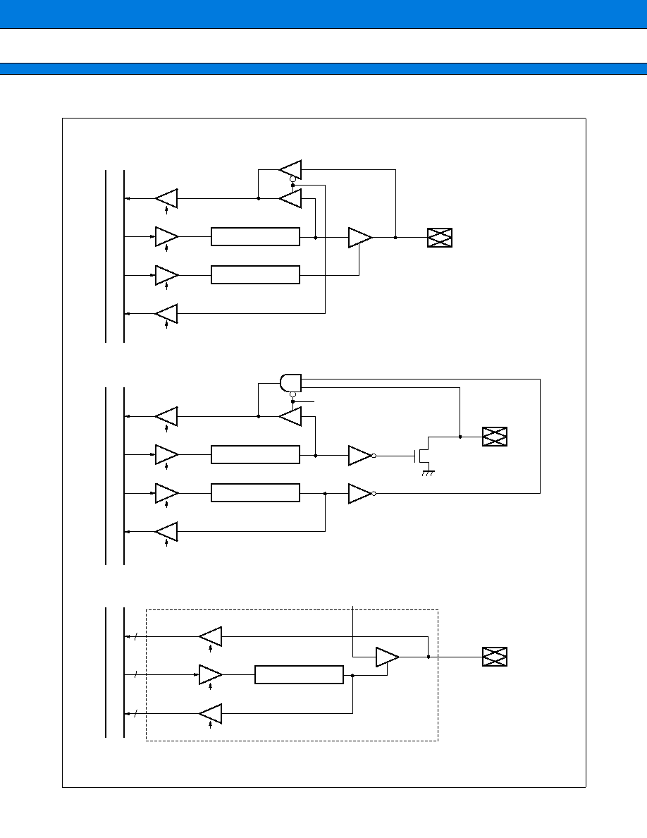
MB90220 Series
36
(2) Block Diagram
Internal data bus
Data register read
Data register write
Direction register write
Direction register read
Data register
Direction register
Pin
Internal data bus
Internal data bus
Data register read
Data register write
ADER register write
ADER register read
Data register
ADER
Pin
RMW
(read-modify-write instruction)
Data register read
Direction register write
Direction register read
Direction register
Pin
Port 7
4
4
4
DOT0 to DOT3 (OCU)
Note: Port 7 is input port. This pin also usable as I/O port for OCU internal function.
∑ I/O Port (Port 0 to 5, 8, and A to C)
∑ I/O Ports with an Open-drain output (Port 6, and 9)
∑ I/O Port (Port 7)
37
MB90220 Series
2. 16-bit Reload Timer (with Event Count Function)
The 16-bit reload timer 1 consists of a 16-bit down counter, a 16-bit reload register, an input pin (TIN), an output
pin (TOT), and a control register. The input clock can be selected from among three internal clocks and one
external clock. At the output pin (TOT), the pulses in the toggled output waveform are output in the reload mode;
the rectangular pulses indicating that the timer is counting are in the single-shot mode. The input pin (TIN) can
be used for event input in the event count mode, and for trigger input or gate input in the internal clock mode.
The MB90220 series has six channels for this timer.
(1) Register Configuration
000041
H
000043
H
000045
H
000047
H
000049
H
00004B
H
--
--
--
--
CSL1
CSL0
MOD2
bit15
bit14
bit13
bit12
bit11
bit10
bit9
MOD1
bit8
(--)
(R/W)
(--)
(--)
(--)
(R/W)
(R/W)
(R/W)
MOD0
OUTE
OUTL
RELD
INTE
UF
CNTE
bit7
bit6
bit5
bit4
bit3
bit2
bit1
TRG
bit0
000040
H
000042
H
000044
H
000046
H
000048
H
00004A
H
001F31
H
001F35
H
001F39
H
001F3D
H
001F41
H
001F45
H
001F30
H
001F34
H
001F38
H
001F3C
H
001F40
H
001F44
H
001F33
H
001F37
H
001F3B
H
001F3F
H
001F43
H
001F47
H
(R)
(R)
(R)
(R)
(R)
(R)
(R)
(R)
(R)
(R)
(R)
(R)
(R)
(R)
(R)
(R)
(W)
(W)
(W)
(W)
(W)
(W)
(W)
(W)
bit15
bit14
bit13
bit12
bit11
bit10
bit9
bit8
TMCSR0
TMCSR1
TMCSR2
TMCSR3
TMCSR4
TMCSR5
- - - - 0000
B
00000000
B
TMCSR0
TMCSR1
TMCSR2
TMCSR3
TMCSR4
TMCSR5
TMR0
TMR1
TMR2
TMR3
TMR4
TMR5
XXXXXXXX
B
TMR0
TMR1
TMR2
TMR3
TMR4
TMR5
bit7
bit6
bit5
bit4
bit3
bit2
bit1
bit0
XXXXXXXX
B
bit15
bit14
bit13
bit12
bit11
bit10
bit9
bit8
XXXXXXXX
B
TMRLR0
TMRLR1
TMRLR2
TMRLR3
TMRLR4
TMRLR5
Register name Address
Register name Address
Register name Address
Register name Address
Register name Address
Initial value
Initial value
(R/W)
(R/W)
(R/W)
(R/W)
(R/W)
(R/W)
(R/W)
(R/W)
Initial value
Initial value
Initial value
∑ Timer Control Status Register 0 to 5 (TMCSR0 to TMCSR5)
∑ 16-bit Timer Register 0 to 5 (TMR0 to TMR5)
∑ 16-bit Timer Reload Register 0 to 5 (TMRLR0 to TMRLR5)
MB90220 Series
38
(2) Block Diagram
(W)
(W)
(W)
(W)
(W)
(W)
(W)
(W)
001F32
H
001F36
H
001F3A
H
001F3E
H
001F42
H
001F46
H
bit7
bit6
bit5
bit4
bit3
bit2
bit1
bit0
XXXXXXXX
B
TMRLR0
TMRLR1
TMRLR2
TMRLR3
TMRLR4
TMRLR5
Register name Address
Initial value
16-bit reload register
16-bit down counter
UF
Reload
OUTE
RELD
OUTL
INTE
UF
EI
2
OS clear
CNTE
TRG
IRQ
Port (TIN)
Port (TOT)
2
Retrigger
3
MOD2
MOD1
MOD0
Prescaler clear
Internal clock
3
EXCK
CSL1
CSL0
GATE
2
Clock selector
2
16
8
16
2
1
2
3
2
5
OUT
CTL.
IN
CTL.
Internal data bus
A/D (timer ch3 output)
UART0 (timer ch5 output)
UART1 (timer ch4 output)
39
MB90220 Series
3. UART0
UART0 is a serial I/O port for synchronous or asynchronous communication with external resources. It has the
following features:
∑ Full duplex double buffer
∑ CLK synchronous and CLK asynchronous data transfers capable
∑ Multiprocessor mode support (Mode 2)
∑ Built-in dedicated baud-rate generator (12 rates)
∑ Arbitrary baud-rate setting from external clock input or internal timer
∑ Variable data length (7 to 9 bits (without parity bit); 6 to 8 bits (with parity bit))
∑ Error detection function (Framing, overrun, parity)
∑ Interrupt function (Two sources for transmission and reception)
∑ Transfer in NRZ format
The MB90220 has three of these modules on chip.
(1) Register Configuration
000020
H
000024
H
000028
H
PEN
SBL
MC1
MC0
SMDE
RFC
SCKE
bit7
bit6
bit5
bit4
bit3
bit2
bit1
SOE
bit0
000022
H
000026
H
00002A
H
D7
D6
D5
D4
D3
D2
D1
D0
bit15
bit14
bit13
bit12
bit11
bit10
bit9
bit8
000021
H
000025
H
000029
H
(R)
(R)
(R)
(R)
(R)
(R/W)
(R/W)
(R)
RDRF
ORFE
PE
TDRE
RIE
TIE
RBF
TBF
000023
H
000027
H
00002B
H
BCH
RC3
RC2
RC1
RC0
BCH0
P
D8
UMC0
UMC1
UMC2
USR0
USR1
USR2
00000100
B
00001000
B
UIDR0/UODR0
UIDR1/UODR1
UIDR2/UODR2
bit7
bit6
bit5
bit4
bit3
bit2
bit1
bit0
XXXXXXXX
B
URD0
URD1
URD2
bit15
bit14
bit13
bit12
bit11
bit10
bit9
bit8
0000000X
B
Register name Address
Serial mode control register
Register name Address
Register name Address
Register name Address
Initial value
Initial value
Initial value
Initial value
(R/W)
(R/W)
(R/W)
(R/W)
(R/W)
(R/W)
(R/W)
(R/W)
(R/W)
(R/W)
(R/W)
(R/W)
(R/W)
(R/W)
(R/W)
(R/W)
(R/W)
(R/W)
(R/W)
(R/W)
(R/W)
(R/W)
(R/W)
(R/W)
∑ Mode Control Register 0 to 2 (UMC0 to UMC2)
∑ Status Register 0 to 2 (USR0 to USR2)
∑ Input Data Register 0 to 2 (UIDR0 to UIDR2)/Ouput Data Register 0 to 2 (UODR0 to UODR2)
∑ Rate and Data Register 0 to 2 (URD0 to URD2)
00002C
H
(--)
(--)
(--)
(R/W)
(R/W)
(R/W)
(--)
(--)
--
--
--
CTE
CSP
CTSE
--
--
UCCR
bit7
bit6
bit5
bit4
bit3
bit2
bit1
bit0
- - - 000 - -
B
Register name Address
Initial value
∑ UART CTS Control Register (UCCR)
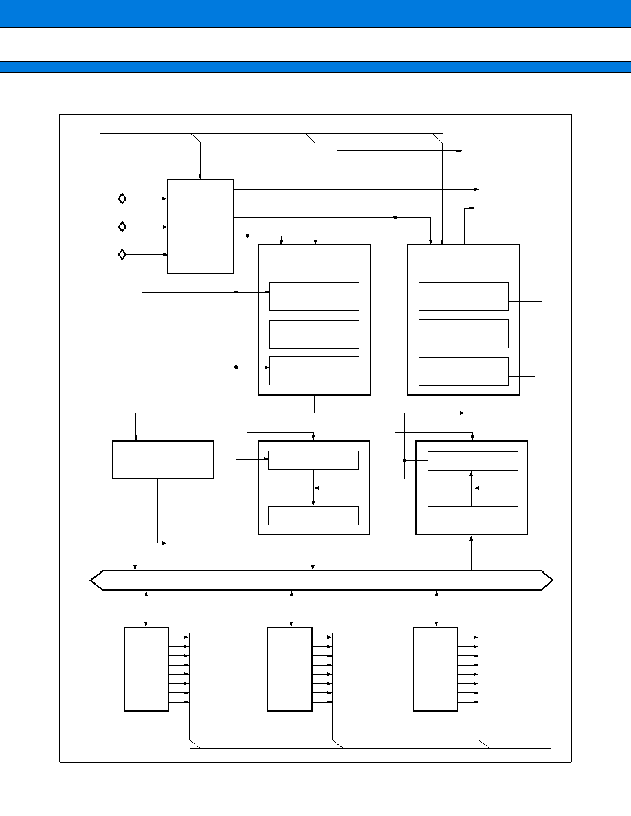
MB90220 Series
40
(2) Block Diagram
CONTROL BUS
Dedicated baud rate clock
16-bit reload timer 5
(internally connected)
External clock
Clock selector
Receiving clock
Transmitting clock
Receiving interrupt
(to CPU)
SCK
Transmission interrupt
(to CPU)
Transmission controller
Transmission
start circuit
Transmitted bit counter
Transmission
parity counter
SOD
Transmitting shifter
UODR
Start of
transmission
Receiving controller
Start bit detector
Received bit counter
Received
parity counter
Receiving shifter
End of
reception
UIDR
Received status
determination circuit
Signal indicating occurrence
of receiving error for EI
2
OS (to CPU)
Internal data bus
UMC
register
USR
register
PEN
SBL
MC1
MC0
SMDE
RFC
SCKE
SOE
RDRF
ORFE
PE
TDRE
RIE
TIE
RBF
TBF
URD
register
BCH
RC3
RC2
RC1
RC0
BCH
P
D8
CONTROL BUS
SID

41
MB90220 Series
4. UART1
The UART1 is a serial I/O port for asynchronous communications (start-stop synchronization) or CLK
synchronized communications. It has the following features:
∑ Full-duplex double buffering
∑ Permits asynchronous (start-stop synchronization) and CLK synchronous communications
∑ Multiprocessor mode support
∑ Built-in dedicated baud rate generator
Asynchronous:
9615, 31250, 4808, 2404, and 1202 bps
CLK synchronization: 1 M, 500 K, 250 K bps
∑ Arbitray baud-rate setting from external clock input or internal timer
∑ Error detection function (parity errors, framing errors, and overrun errors)
∑ Transfer in format NRZ
∑ Extended supports intelligent I/O service
(1) Register Configuration
bit15
bit14
bit13
bit12
bit11
bit10
bit9
PEN
P
SBL
CL
A/D
REC
RXE
TXE
bit8
00002F
H
SCR
00000100
B
bit7
bit6
bit5
bit4
bit3
bit2
bit1
MD1
MD0
CS2
CS1
CS0
BCH
SCKE
SOE
bit0
00002E
H
SMR
00000000
B
D7
D6
D5
D4
D3
D2
D1
D0
000030
H
SIDR
XXXXXXXX
B
D7
D6
D5
D4
D3
D2
D1
D0
000030
H
SODR
XXXXXXXX
B
PE
ORE
FRE
RDRF
TDRE
--
RIE
TIE
000031
H
SSR
00001-00
B
bit7
bit6
bit5
bit4
bit3
bit2
bit1
bit0
bit7
bit6
bit5
bit4
bit3
bit2
bit1
bit0
bit15
bit14
bit13
bit12
bit11
bit10
bit9
bit8
Register name Address
Register name Address
Register name Address
Register name Address
Register name Address
Initial value
Initial value
Initial value
Initial value
(R/W)
(R/W)
(R/W)
(R/W)
(R/W)
(R/W)
(R/W)
(R/W)
(R/W)
(R/W)
(R/W)
(R/W)
(R/W)
(R)
(R/W)
(R/W)
(W)
(W)
(W)
(W)
(W)
(W)
(W)
(W)
(R)
(R)
(R)
(R)
(R)
(R)
(R)
(R)
(R)
(R)
(R)
(R)
(R)
(R/W)
(R/W)
∑ Mode Register (SMR)
∑ SCR (Control Register)
∑ Input Data Register (SIDR)/Serial Output Data Register (SODR)
∑ SSR (Status Register)
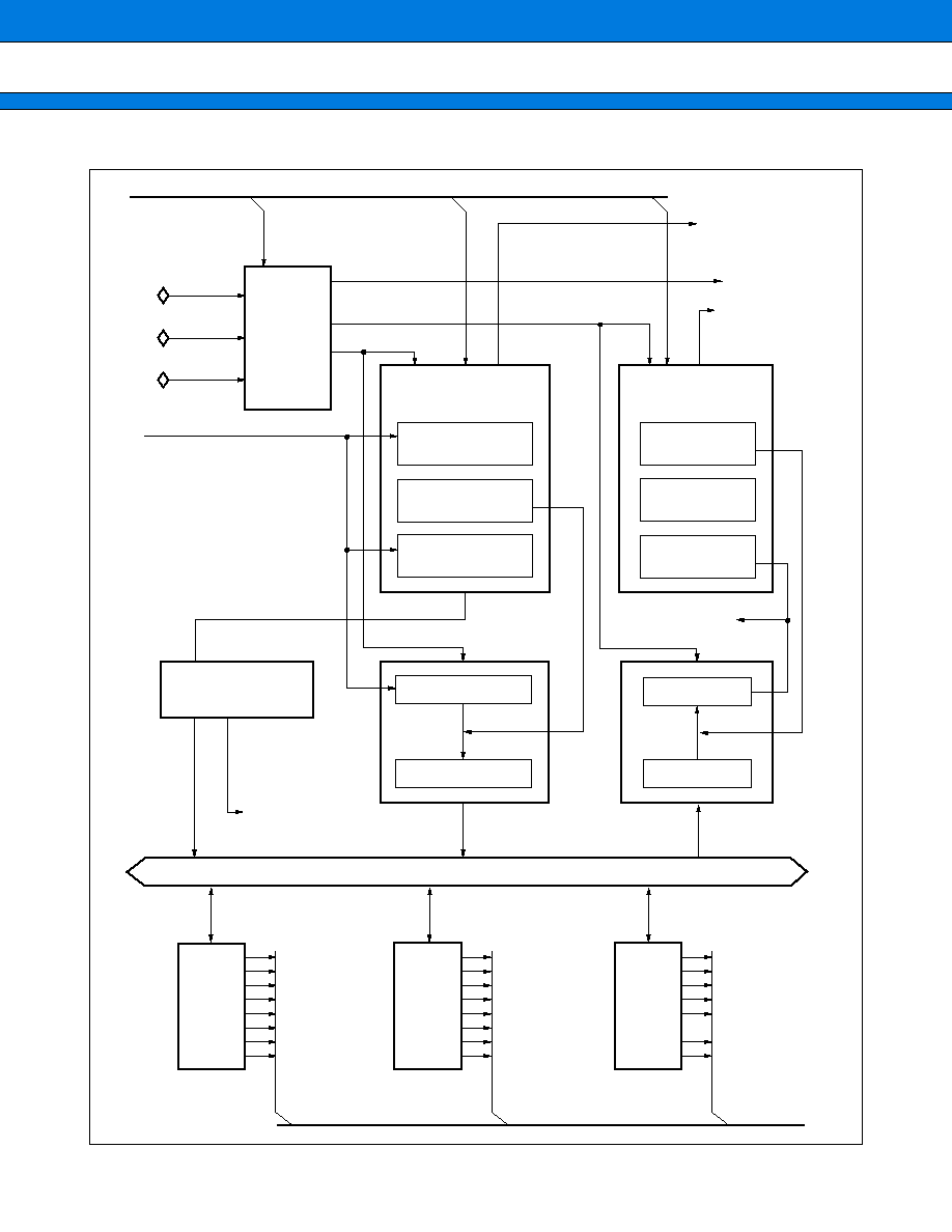
MB90220 Series
42
(2) Block Diagram
Control signals
Dedicated baud rate generator
External clock
Clock selector
Receiving clock
Transmitting clock
Receiving interrupt
(to CPU)
SCK3
Transmission interrupt
(to CPU)
Transmission controller
Transmission
start circuit
Transmitted
bit counter
Transmission
parity counter
SOD3
Transmitting shifter
SODR
Start of
transmission
Receiving controller
Start bit detector
Received
bit counter
Received
parity counter
Receiving shifter
End of
reception
SIDR
Received status
determination circuit
Signal indicating occurrence
of receiving error for EI
2
OS (to CPU)
Internal data bus
SMR
register
SCR
register
MD1
MD0
CS2
CS1
CS0
BCH
SCKE
SOE
PEN
P
SBL
CL
A/D
REC
RXE
TXE
SSR
register
PE
ORE
FRE
RDRF
TDRE
RIE
TIE
Control signals
SID3
16-bit reload timer 4
(internally connected)

43
MB90220 Series
5. 10-bit A/D Converter
The 10-bit A/D converter converts analog input voltage into a digital value. The features of this module are
described below:
∑ Conversion time: 6.125
µ
s/channel (min.) (with machine clock running at 16 MHz)
∑ Uses RC-type sequential comparison and conversion method with built-in sample and hold circuit
∑ 10-bit resolution
∑ Analog input can be selected by software from among 16 channels
Single-conversion mode:
Selects and converts one channel.
Scan conversion mode:
Converts several consecutive channels (up to 16 can be programmed).
One-shot mode:
Converts the specified channel once and terminates.
Continuous conversion mode: Repeatedly converts the specified channel.
Stop conversion mode:
Pauses after converting one channel and waits until the next startup (permits
synchronization of start of conversion).
∑ When A/D conversion is completed, an "A/D conversion complete" interrupt request can be issued to the CPU.
Because the generation of this interrupt can be used to start up the EI
2
OS and transfer the A/D conversion
results to memory, this function is suitable for continuous processing.
∑ Startup triggers can be selected from among software, an external trigger (falling edge), and a timer (rising
edge).
(1) Register Configuration
bit7
bit6
bit5
bit4
bit3
bit2
bit1
ANS3
ANS2
ANS1
ANS0
ANE3
ANE2
ANE1
ANE0
bit0
000032
H
ADCH
00000000
B
bit15
bit14
bit13
bit12
bit11
bit10
bit9
--
--
--
MOD1
MOD0
STS1
STS0
bit8
(R/W)
(--)
(R/W)
(--)
(--)
(W)
(R/W)
(R/W)
BUSY
INT
INTE
PAUS
--
--
STRT
(--)
(R/W)
(W)
(R/W)
(R/W)
(R/W)
(--)
(R/W)
D7
D6
D5
D4
D3
D2
D1
D0
000033
H
ADMD
- - - X0000
B
bit7
bit6
bit5
bit4
bit3
bit2
bit1
bit0
000034
H
ADCS
0000 - - 00
B
XXXXXXXX
B
000036
H
ADCD
bit7
bit6
bit5
bit4
bit3
bit2
bit1
bit0
Register name Address
This register specfies the A/D converter conversion channel.
This register specfies the A/D converter operation mode and the startup source.
This register is the A/D converter control and status register.
Note: Program "0" to bit 12 when write. Read value is indeterminated.
This register stores the A/D converter conversion data.
Register name Address
Register name Address
Register name Address
Initial value
Initial value
Initial value
Initial value
(R/W)
(R/W)
(R/W)
(R/W)
(R/W)
(R/W)
(R/W)
(R/W)
Reserved
Reserved
(R)
(R)
(R)
(R)
(R)
(R)
(R)
(R)
∑ A/D Channel Setting Register (ADCH)
∑ A/D Mode Register (ADMD)
∑ A/D Control Status Register (ADCS)
∑ A/D Data Register (ADCD)
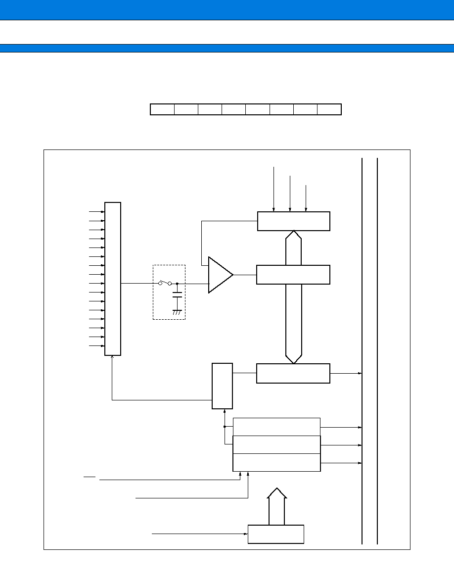
MB90220 Series
44
(2) Block Diagram
D9
D8
--
--
--
--
--
--
000037
H
ADCD
bit15
bit14
bit13
bit12
bit11
bit10
bit9
bit8
000000XX
B
Register name Address
Initial value
(R)
(R)
(R)
(R)
(R)
(R)
(R)
(R)
MPX
AN0
AN1
AN2
AN3
AN4
AN5
AN6
AN7
AN8
AN9
AN10
AN11
AN12
AN13
AN14
AN15
Comparator
Sample and hold circuit
AVCC
AVRH/AVRL
AV
SS
D/A converter
Sequential
comparison register
A/D data register
ADCD
ADCH
ADMD
ADCS
A/D channel setting register
A/D mode register
A/D control status register
Operation clock
Prescaler
Timer
(16-bit reload timer 3 output)
Timer startup
Machine clock
ATG
Trigger startup
Input circuit
Decoder
Internal data bus
45
MB90220 Series
6. PWC (Pulse Width Count) Timer
The PWC (pulse width count) timer is a 16-bit multifunction up-count timer with an input-signal pulse-width count
function and a reload timer function. The hardware configuration of this module is a 16-bit up-count timer, an
input pulse divider with divide ratio control register, four count input pins, and a 16-bit control register. Using
these components, the PWC timer provides the following features:
∑ Timer functions:
An interrupt request can be generated at set time intervals.
Pulse signals synchronized with the timer cycle can be output.
The reference internal clock can be selected from among three internal clocks.
∑ Pulse-width count functions:
The time between arbitrary pulse input events can be counted.
The reference internal clock can be selected from among three internal clocks.
Various count modes:
"H" pulse width (
to
)/"L" pulse width (
to
)
Rising-edge cycle (
to
/Falling-edge cycle (
to
)
Count between edges (
or
to
or
)
Cycle count can be performed by 2
2n
division (n = 1, 2, 3, 4) of the input
pulse, with an 8 bit input divider.
An interrupt request can be generated once counting has been performed.
The number of times counting is to be performed (once or subsequently) can
be selected.
The MB90220 series has four channels for this module.
(1) Register Configuration
bit15
bit14
bit13
bit12
bit11
bit10
bit9
STRT
STOP
EDIR
EDIE
OVIR
OVIE
ERR
POUT
bit8
000051
H
000053
H
000055
H
000057
H
bit7
bit6
bit5
bit4
bit3
bit2
bit1
CKS1
CKS0
PIS1
PIS0
S/C
MOD1
MOD1
MOD0
bit0
000050
H
000052
H
000054
H
000056
H
001F01
H
001F03
H
001F05
H
001F07
H
001F00
H
001F02
H
001F04
H
001F06
H
PWCSR0
PWCSR1
PWCSR2
PWCSR3
00000000
B
PWCSR0
PWCSR1
PWCSR2
PWCSR3
00000000
B
PWCR0
PWCR1
PWCR2
PWCR3
00000000
B
PWCR0
PWCR1
PWCR2
PWCR3
00000000
B
bit7
bit6
bit5
bit4
bit3
bit2
bit1
bit0
Register name Address
Register name Address
Register name Address
Register name Address
(R/W)
(R/W)
(R)
(R/W)
(R/W)
(R/W)
(R)
(R/W)
Initial value
Initial value
Initial value
Initial value
bit15
bit14
bit13
bit12
bit11
bit10
bit9
bit8
(R/W)
(R/W)
(R/W)
(R/W)
(R/W)
(R/W)
(R/W)
(R/W)
(R/W)
(R/W)
(R/W)
(R/W)
(R/W)
(R/W)
(R/W)
(R/W)
(R/W)
(R/W)
(R/W)
(R/W)
(R/W)
(R/W)
(R/W)
(R/W)
∑ PWC Control Status Register 0 to 3 (PWCSR0 to PWCSR3)
∑ PWC Data Buffer Register 0 to 3 (PWCR0 to PWCR3)
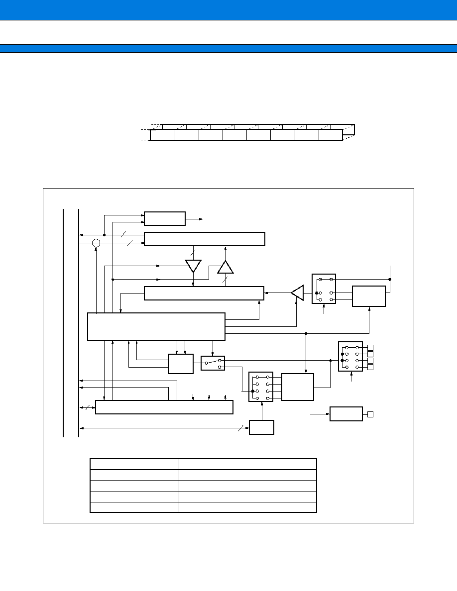
MB90220 Series
46
(2) Block Diagram
00007A
H
00007C
H
00007E
H
000080
H
(R/W)
(R/W)
bit7
bit6
bit5
bit4
bit3
bit2
bit1
bit0
DIVR0
DIVR1
DIVR2
DIVR3
- - - - - - 00
B
Register name Address
Initial value
--
--
--
--
--
--
MOD1
MOD0
(--)
(--)
(--)
(--)
(--)
(--)
∑ PWC Division Ratio Control Register 0 to 3 (DIVR0 to DIVR3)
Clock divider
Internal clock
(machine clock/4)
2
3
2
2
CKS 1
CKS 0
Divider clear
PIS 1
PIS 0
PWC 0
PWC 1
PWC 2
PWC 3
*
F.F.
POT
Overflow
DIVR
2
15
PWCSR
Overflow interrupt
request
Count end interrupt request
Count end edge
Count
start edge
Edge
detector
Start edge
select
End edge
select
ERR
PIS 1
PIS 0
CKS 1
CKS 0
Divider
selection
8-bit
divider
Division on/off
Controller
16-bit up-count timer
16
Error detector
PWCR
16
16
16
Timer clear
Count enable
Clock
Overflow
Data transfer
Reload
ERR
PWCR read
Internal data bus
Flag set, etc.
Write enable
Control bit output
*: In the MB90220 series, only the module input PWC 0 of each channel is connected to the respective external pins.
Channel
POT pin
PWC ch. 0
PWC ch. 1
PWC ch. 2
PWC ch. 3
PA 1/PWC 0/POT 0
PA 2/PWC 1/POT 1/ASR 1
PA 3/PWC 2/POT 2/ASR 2
PA 4/PWC 3POT 3/ASR 3
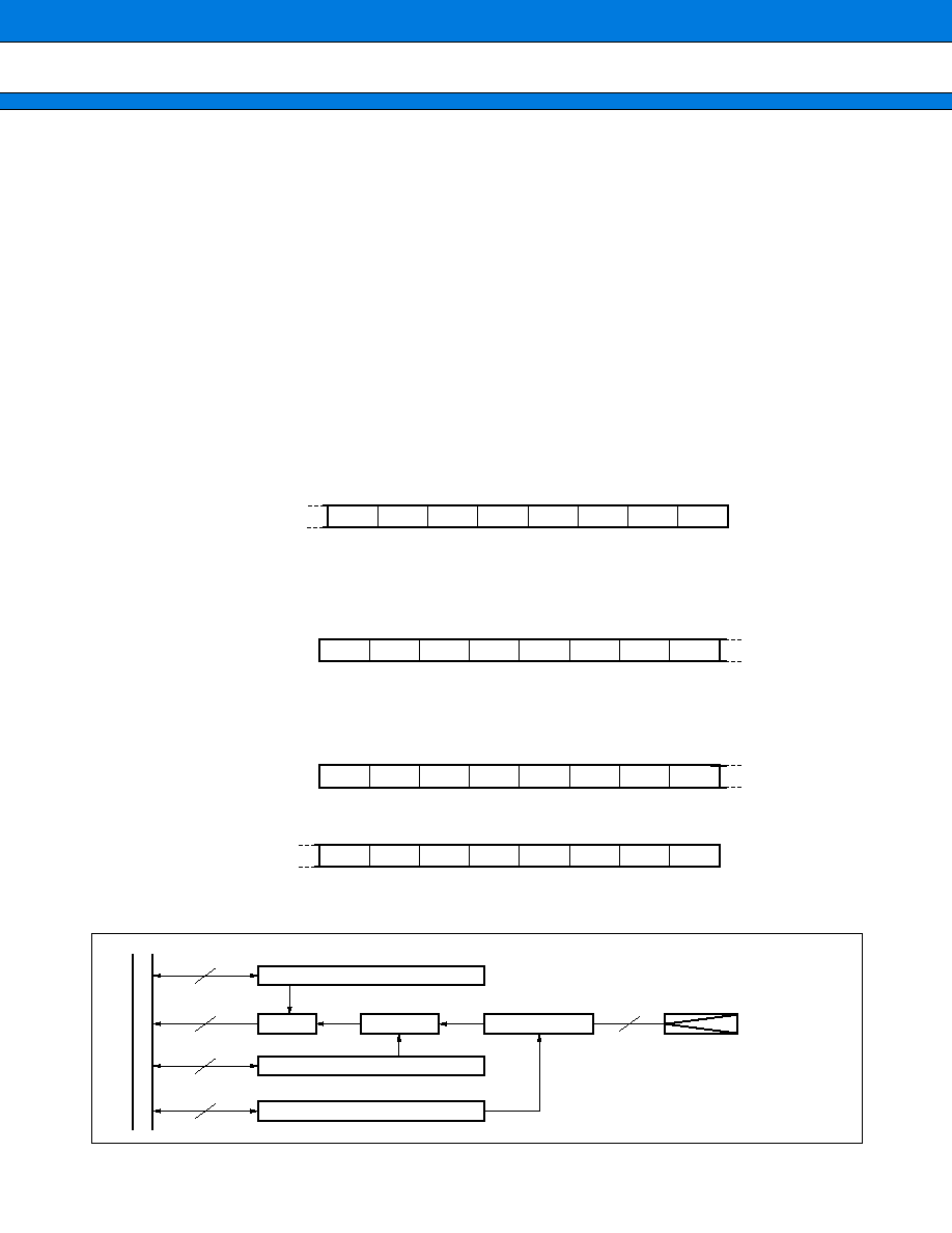
47
MB90220 Series
7. DTP/External Interrupts
DTP (Data Transfer Peripheral) is located between external peripherals and the F
2
MC-16F CPU. It receives a
DMA request or an interrupt request generated by the external peripherals and reports it to the F
2
MC-16F CPU
to activate the extended intelligent I/O service or interrupt handler. The user can select two request levels of "H"
and "L" for extended intelligent I/O service or, and four request levels of "H," "L," rising edge and falling edge for
external interrupt requests. In MB90220, only parts corresponding to INT2 to INT0 are usable as external
interrupt/DTP request.
Parts corresponding to INT7 to INT3 cannot be used as external interrupt/DTP request, but only for edge
detection at external terminals.
Note: INT7 to INT3 are not usable as DTP/external interrupts.
(1) Register Configuration
(2) Block Diagram
bit15
bit14
bit13
bit12
bit11
bit10
bit9
ER7
ER6
ER5
ER4
ER3
ER2
ER1
ER0
bit8
00003A
H
bit7
bit6
bit5
bit4
bit3
bit2
bit1
EN7
EN6
EN5
EN4
EN3
EN2
EN1
EN0
bit0
00003B
H
LB7
LA7
LB6
LA6
LB5
LA5
LB4
LA4
00003D
H
00003C
H
LB3
LA3
LB2
LA2
LB1
LA1
LB0
LA0
ENIR
00000000
B
00000000
B
EIRR
bit15
bit14
bit13
bit12
bit11
bit10
bit9
bit8
00000000
B
ELVR
ELVR
bit7
bit6
bit5
bit4
bit3
bit2
bit1
bit0
00000000
B
Register name Address
Register name Address
Register name Address
Register name Address
Initial value
Initial value
Initial value
Initial value
(R/W)
(R/W)
(R/W)
(R/W)
(R/W)
(R/W)
(R/W)
(R/W)
(R/W)
(R/W)
(R/W)
(R/W)
(R/W)
(R/W)
(R/W)
(R/W)
(R/W)
(R/W)
(R/W)
(R/W)
(R/W)
(R/W)
(R/W)
(R/W)
(R/W)
(R/W)
(R/W)
(R/W)
(R/W)
(R/W)
(R/W)
(R/W)
∑ DTP/Interrupt Enable Register (ENIR)
∑ Request Level Setting Register (ELVR)
∑ DTP/Interrupt Source Register (EIRR)
Interrupt/DTP enable register
4
Gate
4
Source F/F
Edge detector
8
Interrupt/DTP source register
4
Request level setting register
8
INT
Internal data bus
MB90220 Series
48
8. 24-bit Timer Counter
The 24-bit timer counter consists of a 24-bit up-counter, an 8-bit output buffer register, and a control register.
The count value output by this timer counter is used to generate the base time used for input capture and output
compare.
The interrupt functions provided are timer overflow interrupts and timer intermediate bit interrupts. The
intermediate bit interrupt permits four time settings.
The 24-bit timer counter value is cleared to all zeroes by a reset.
(1) Register Configuration
TCCR
000071
H
bit15
bit14
bit13
bit12
bit11
bit10
bit9
--
--
--
PR0
bit8
(R/W)
(--)
(R/W)
(--)
(W)
(W)
(R/W)
(R/W)
bit7
bit6
bit5
bit4
bit3
bit2
bit1
CLR2
CLR
IVF
IVFE
TIM
TIME
TIS1
TIS0
bit0
(R/W)
(W)
(R/W)
(W)
(R/W)
(R/W)
(R/W)
(R/W)
TCRL
000072
H
000073
H
00000000
B
TCRL
bit15
bit0
TCRH
000074
H
000075
H
00000000
B
TCRH
bit15
bit0
bit8 bit7
TCCR
000070
H
- - 111111
B
11000000
B
Access
R
Access
R
Register name Address
Register name Address
Register name Address
Register name Address
Initial value
Initial value
Initial value
Initial value
Reserved Reserved Reserved
Reserved
Reserved
∑ Free-run Timer Control Register (TCCR)
∑ Free-run Timer Low-order Data Register (TCRL)
∑ Free-run Timer High-order Data Register (TCRH)
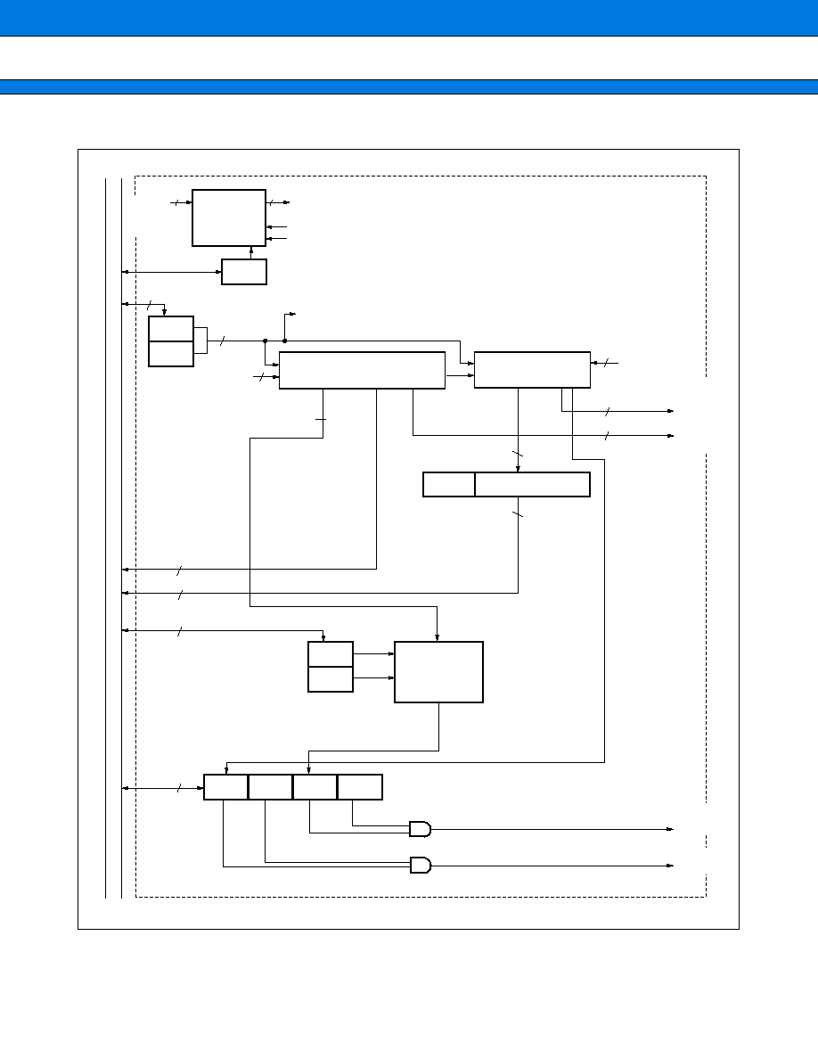
49
MB90220 Series
(2) Block Diagram
2
Internal
basic
clock
/3
/4
2
Timer counter clocks
CK0
PR0
2
Clear bit
CLR
CLR2
2
CK0
CK1
2
Lower-order 16-bit counter
4
CLR/CLR2
Higher-order 8-bit counter
Carry
2
8
16
CK0, CK1
Timer counter bit output
T23 to T16
T0 to T15
Output buffer
8
16
23rd bit
16
16
2
4
TIS1
TIS0
Intermediate bit interrupt
cycle setting
10th bit
11th bit
12th bit
13th bit
Interrupt enable
Interrupt flag
IVF
IVFE
TIM
TIME
Intermediate bit interrupt request
Overflow interrupt request
TIM
IVF
Internal data bus
CK1
CLR (prescaler clear)
CLR2 (prescaler clear, 24-bit timer counter STOP bit)
"0"
MB90220 Series
50
9. OCU (Output Compare Unit)
The OCU (Output Compare Unit) consists of a 24-bit output compare register, a comparator, and a control
register.
The match detection signal is output when the contents of the output compare register match the contents of
the 24-bit timer counter. This match detection signal can be used to change the output value of the corresponding
pin, or can be used to generate an interrupt. One block consists of four output compare units, and the four
output compare registers use one comparator to perform time division comparisons.
(1) Register Configuration
bit15
bit14
bit13
bit12
bit11
bit10
bit9
bit8
bit15
bit14
bit13
bit12
bit11
bit10
bit9
bit8
000061
H
000063
H
(--)
(--)
(--)
(--)
(R/W)
(R/W)
(R/W)
(R/W)
(--)
(--)
(--)
(--)
(R/W)
(R/W)
(R/W)
(R/W)
--
--
--
--
MD3
MD2
MD1
MD0
000060
H
000062
H
SEL3
SEL2
SEL1
SEL0
CPE3
CPE2
CPE1
CPE0
bit7
bit6
bit5
bit4
bit3
bit2
bit1
bit0
bit15
bit14
bit13
bit12
bit11
bit10
bit9
bit8
000069
H
00006B
H
ICE3
ICE2
ICE1
ICE0
IC3
IC2
IC1
IC0
000068
H
00006A
H
--
--
--
--
DOT3
DOT2
DOT1
DOT0
001F11
H
001F15
H
001F19
H
001F1D
H
001F21
H
001F25
H
001F29
H
001F2D
H
001F10
H
001F14
H
001F18
H
001F1C
H
001F20
H
001F24
H
001F28
H
001F2C
H
--
--
CCR00
CCR02
CCR00
CCR02
- - - - 0000
CCR10
CCR11
11110000
bit7
bit6
bit5
bit4
bit3
bit2
bit1
bit0
CCR10
CCR11
00000000
- - - - 0000
CPR00L
CPR01L
CPR02L
CPR03L
CPR04L
CPR05L
CPR06L
CPR07L
CPR00L
CPR01L
CPR02L
CPR03L
CPR04L
CPR05L
CPR06L
CPR07L
bit7
bit6
bit5
bit4
bit3
bit2
bit1
bit0
00000000
00000000
Register name Address
Register name Address
Register name Address
Register name Address
Register name Address
Register name Address
Initial value
Initial value
Initial value
Initial value
Initial value
Initial value
(R/W)
(R/W)
(R/W)
(R/W)
(R/W)
(R/W)
(R/W)
(R/W)
(R/W)
(R/W)
(R/W)
(R/W)
(R/W)
(R/W)
(R/W)
(R/W)
(R/W)
(R/W)
(R/W)
(R/W)
(R/W)
(R/W)
(R/W)
(R/W)
(R/W)
(R/W)
(R/W)
(R/W)
(R/W)
(R/W)
(R/W)
(R/W)
∑ OCUO Control Register 00, 01 (CCR00, CCR01)
∑ OCUO Control Register 10, 11 (CCR10, CCR11)
∑ OCU Compare Low-order Data Register 00 to 07 (CPR00L to CPR07L)
51
MB90220 Series
001F13
H
001F17
H
001F1B
H
001F1F
H
001F23
H
001F27
H
001F2B
H
001F2F
H
001F12
H
001F16
H
001F1A
H
001F1E
H
001F22
H
001F26
H
001F2A
H
001F2E
H
--
--
CPR00
CPR01
CPR02
CPR03
CPR04
CPR05
CPR06
CPR07
CPR00
CPR01
CPR02
CPR03
CPR04
CPR05
CPR06
CPR07
bit15 bit14 bit13 bit12 bit11 bit10 bit9 bit8
bit7
bit6
bit5
bit4
bit3
bit2
bit1
bit0
00000000
00000000
Register name Address
Register name Address
Initial value
Initial value
(R/W)
(R/W)
(R/W)
(R/W)
(R/W)
(R/W)
(R/W)
(R/W)
(R)
(R)
(R)
(R)
(R)
(R)
(R)
(R)
∑ Output Compare High-order Data Register 00 to 07 (CPR00H to CPR07H)
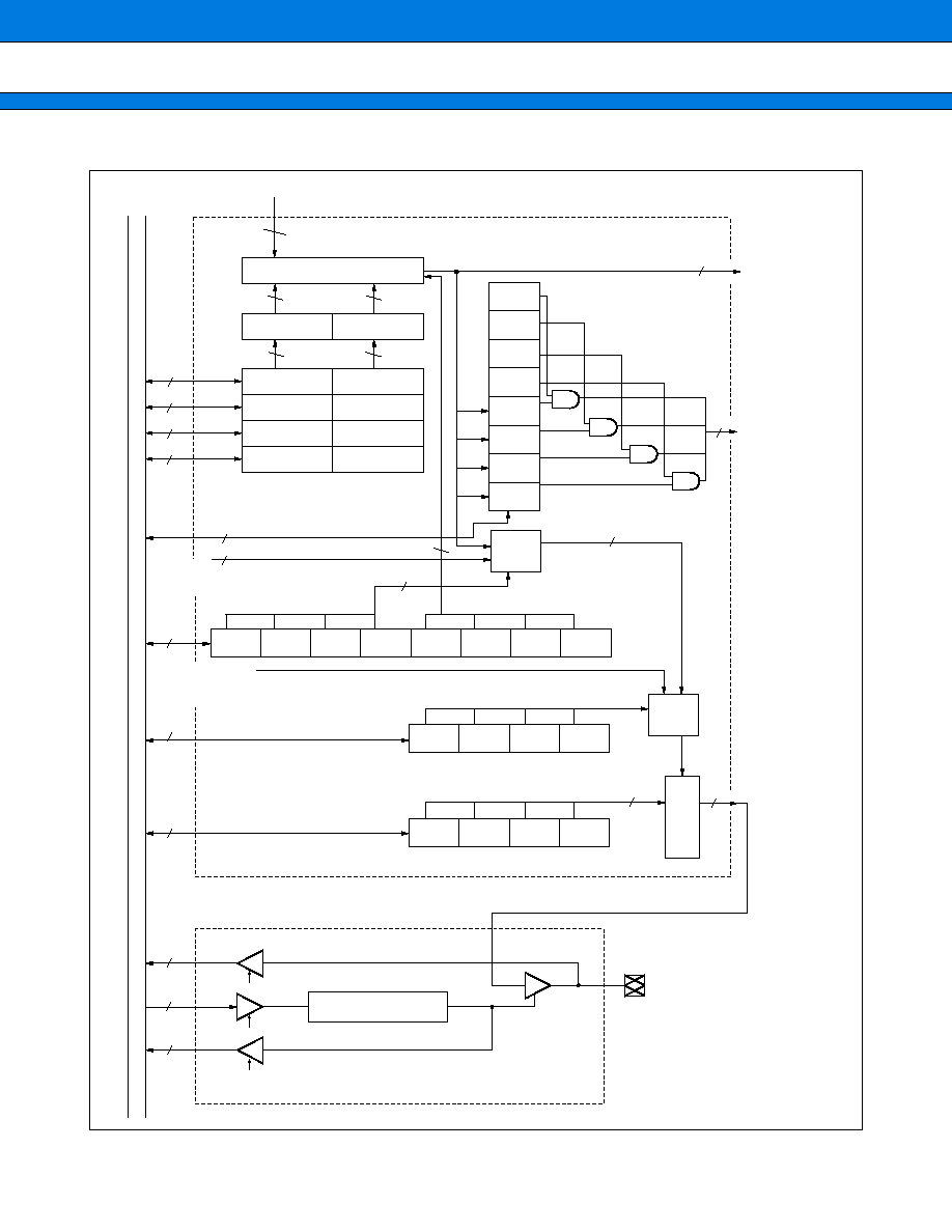
MB90220 Series
52
(2) Block Diagram
(Continued)
24-bit timer counter
Internal data bus
22
T2 to T23
Comparator controller
24
24
24
24
8
14
Output latch
Output latch
8
14
CPR03
CPR02
CPR01
CPR00
CPR03L
CPR02L
CPR01L
CPR00L
8
4
Output
compare register
higher-order 8 bits
Output
compare register
lower-order 16 bits
4
Match source signals
EXT0 to 3
8
4
4
Match detection signal selection
4
SEL3
SEL2
SEL1
SEL0
CPE3
CPE2
CPE1
CPE0
Match operation enable
Source
selector
Clock
selector
Output latch
4
4
DOT0 to 3
MD3
MD2
MD1
MD0
DOT3
DOT2
DOT1
DOT0
DOT pin data output
(also serves as general-purpose port data register)
Port general purpose/compare dedicated switching
4
4
4
ICMP0 to 3
Interrupt
request signals
MATCH0 to 3
Interrupt enable ICE0 to 3
Match signal
ICE3
ICE2
ICE1
ICE0
IC3
IC2
IC1
IC0
Interrupt flags IC0 to 3
24-bit timer counter
data T0
4
4
4
Direction register
Data register read
Direction register write
Direction register read
Pin
Port 7
Compare unit*
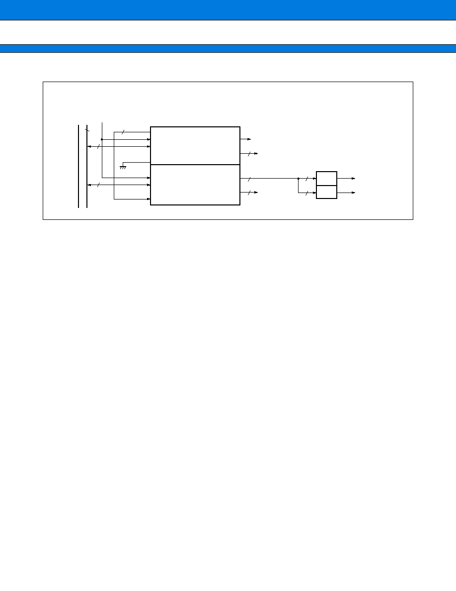
53
MB90220 Series
(Continued)
Internal data bus
timer count data
16
Compare unit
MATCH 0 to 3
T1 to T23
RB15 to 0
EXT 0 to 3
ICOMP 0 to 3
DOT 0 to 3
Compare 00 to 03
MATCH 0 to 3
T1 to T23
RB15 to 0
EXT 0 to 3
ICOMP 0 to 3
DOT 0 to 3
Compare 10 to 13
4
16
23
OPEN
Interrupt request ICOMP 0 to 3
4
4
4
Pin output
DOT 0 to 3
ICOMP 0, 2
Pin output
DOT 4 to 7
OR
OR
2
2
ICOMP 1, 3
ICOMP 4/6
ICOMP 5/7
Interrupt request
*: There are two compare units drawn as below.
MB90220 Series
54
10. ICU (Input Capture Unit)
This module detects either the rising edge, falling edge, or both edges of an externally input waveform and holds
the value of the 24-bit timer counter at that time, while at the same time the module generates an interrupt
request for the CPU. The module consists of a 24-bit input capture data register and a control register. There
are four external input pins (ASR0 to ASR3); the operation of each input is described below.
ASR0 to ASR3: Each of these input pins has a corresponding input capture register. When the specified
valid edge (
or
or
) is detected, the register can be used to store the 24-bit timer
counter value.
(1) Register Configuration
000058
H
EG3B
EG3A
EG2B
EG2A
EG1B
EG1A
EG0B
EG0A
00005A
H
IRE3
IRE2
IRE1
IRE0
IR3
IR2
IR1
IR0
001F50
H
001F54
H
001F58
H
001F5C
H
bit7
bit6
bit5
bit4
bit3
bit2
bit1
bit0
D07
D06
D05
D04
D03
D02
D01
D00
D15
D14
D13
D12
D11
D10
D09
bit15
bit14
bit13
bit12
bit11
bit10
bit9
D08
bit8
001F52
H
001F56
H
001F5A
H
001F5E
H
D23
D22
D21
D20
D19
D18
D17
D16
--
--
--
--
--
--
--
--
ICCO
bit7
bit6
bit5
bit4
bit3
bit2
bit1
bit0
ICCI
00000000
B
00000000
B
ICRL0
ICRL1
ICRL2
ICRL3
XXXXXXXX
B
001F51
H
001F55
H
001F59
H
001F5D
H
ICRL0
ICRL1
ICRL2
ICRL3
XXXXXXXX
B
ICRH0
ICRH1
ICRH2
ICRH3
bit7
bit6
bit5
bit4
bit3
bit2
bit1
bit0
bit7
bit6
bit5
bit4
bit3
bit2
bit1
bit0
bit15
bit14
bit13
bit12
bit11
bit10
bit9
bit8
XXXXXXXX
B
00000000
B
001F53
H
001F57
H
001F5B
H
001F5F
H
ICRH0
ICRH1
ICRH2
ICRH3
Register name Address
Register name Address
Register name Address
Register name Address
Register name Address
Register name Address
(R/W)
(R/W)
(R/W)
(R/W)
(R/W)
(R/W)
(R/W)
(R/W)
(R/W)
(R/W)
(R/W)
(R/W)
(R/W)
(R/W)
(R/W)
(R/W)
Initial value
Initial value
Initial value
Initial value
Initial value
Initial value
(R)
(R)
(R)
(R)
(R)
(R)
(R)
(R)
(R)
(R)
(R)
(R)
(R)
(R)
(R)
(R)
(R)
(R)
(R)
(R)
(R)
(R)
(R)
(R)
(R)
(R)
(R)
(R)
(R)
(R)
(R)
(R)
∑ ICU Control Register 0 (ICC0)
∑ ICU Control Register 1 (ICC1)
∑ ICU Low-order Data Register (ICRL0 to ICRL3)
∑ ICU High-order Data Register (ICRH0 to ICRH3)
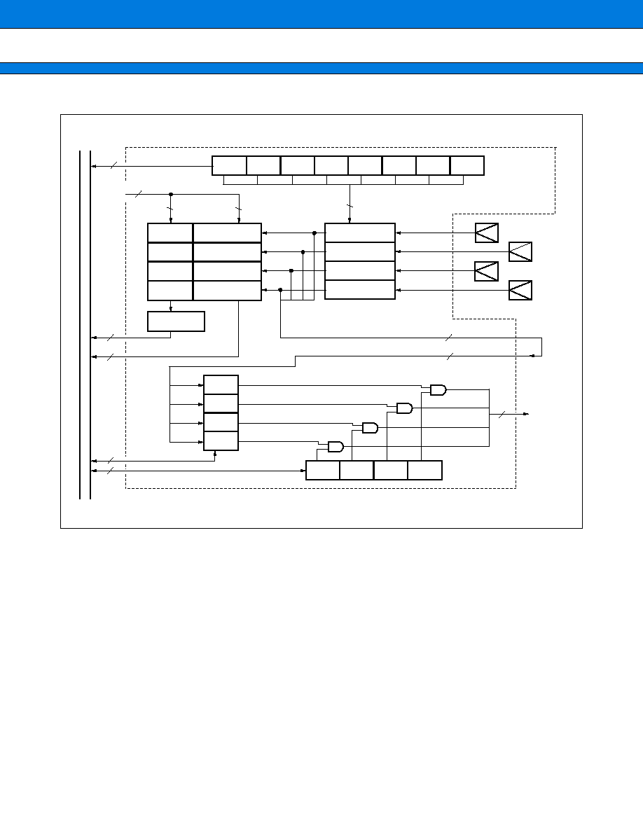
55
MB90220 Series
(2) Block Diagram
8
24-bit timer counter input
T23
to T0
24
16
T23 to
T16
T15 to T00
4
16
Output latch
IR0
IR1
IR2
IR3
Interrupt request flags (ICC1)
4
Capture
8
EG3B
EG3A
EG2B
EG2A
EG1B
EG1A
EG0B
EG0A
8
ICRH0
ICRH1
ICRH2
ICRH3
ICRL0
ICRL1
ICRL2
ICRL3
Edge detection 0
Edge detection 1
Edge detection 2
Edge detection 3
Edge detection 0 to 3:
or
or
4
4
IRE3
IRE2
IRE1
IRE0
Interrupt enable
(ICC1)
4
IRQ0 to IRQ3
EGI0 to EGI3
EGO0 to EGO3
ASR3
ASR2
ASR1
ASR0
Edge detection
polarity (ICC0)
8
Internal data bus
MB90220 Series
56
11. 16-bit PPG Timer
This module can output a pulse synchronized with an external trigger or a software trigger. In addition, the cycle
and duty ratio of the output pulse can be changed as desired by overwriting the two 16-bit register values.
PWM function:
Synchronizes pulse with trigger, and permits programming of the pulse output by
overwriting the register values mentioned above.
This function permits use as a D/A converter with the addition of external circuits.
One-shot function: Detects the edge of trigger input, and permits single-pulse output. There is no
trigger input for PPG1.
This module consists of a 16-bit down-counter, a prescaler, a 16-bit synchronization setting register, a 16-bit
duty register, a 16-bit control register, one external trigger input pin, and one PPG output pin.
(1) Register Configuration
0004D
H
0004F
H
CNTE
STGR
MDSE
RTRG
CKS1
CKS0
PGMS
--
bit15
bit14
bit13
bit12
bit11
bit10
bit9
bit8
0004C
H
0004E
H
EGS1
EGS0
IREN
IRQF
IRS1
IRS0
POEN
OSEL
bit7
bit6
bit5
bit4
bit3
bit2
bit1
bit0
001F49
H
001F4D
H
001F48
H
001F4C
H
001F4B
H
001F4F
H
001F4A
H
001F4E
H
PCNT0
PCNT1
PCNT0
PCNT1
00000000
B
00000000
B
bit15
bit14
bit13
bit12
bit11
bit10
bit9
bit8
bit15
bit14
bit13
bit12
bit11
bit10
bit9
bit8
bit7
bit6
bit5
bit4
bit3
bit2
bit1
bit0
bit7
bit6
bit5
bit4
bit3
bit2
bit1
bit0
XXXXXXXX
B
XXXXXXXX
B
XXXXXXXX
B
XXXXXXXX
B
PCSP0
PCSP1
PDUT0
PDUT1
PDUT0
PDUT1
PCSP0
PCSP1
Register name Address
Register name Address
Register name Address
Register name Address
Register name Address
Register name Address
Initial value
Initial value
Initial value
Initial value
Initial value
Initial value
(R/W)
(R/W)
(R/W)
(R/W)
(R/W)
(R/W)
(R/W)
(R/W)
(R/W)
(R/W)
(R/W)
(R/W)
(R/W)
(R/W)
(R/W)
(W)
(W)
(W)
(W)
(W)
(W)
(W)
(W)
(W)
(W)
(W)
(W)
(W)
(W)
(W)
(W)
(W)
(W)
(W)
(W)
(W)
(W)
(W)
(W)
(W)
(W)
(W)
(W)
(W)
(W)
(W)
(W)
Overwrite during operation
Overwrite during operation
∑ PPG Control Status Register (PCNT0, PCNT1)
∑ PPG0, PPG1 Cycle Setting Register (PCSP0, PCSP1)
∑ PPG0, PPG1 Duty Setting Register (PDUT0, PDUT1)
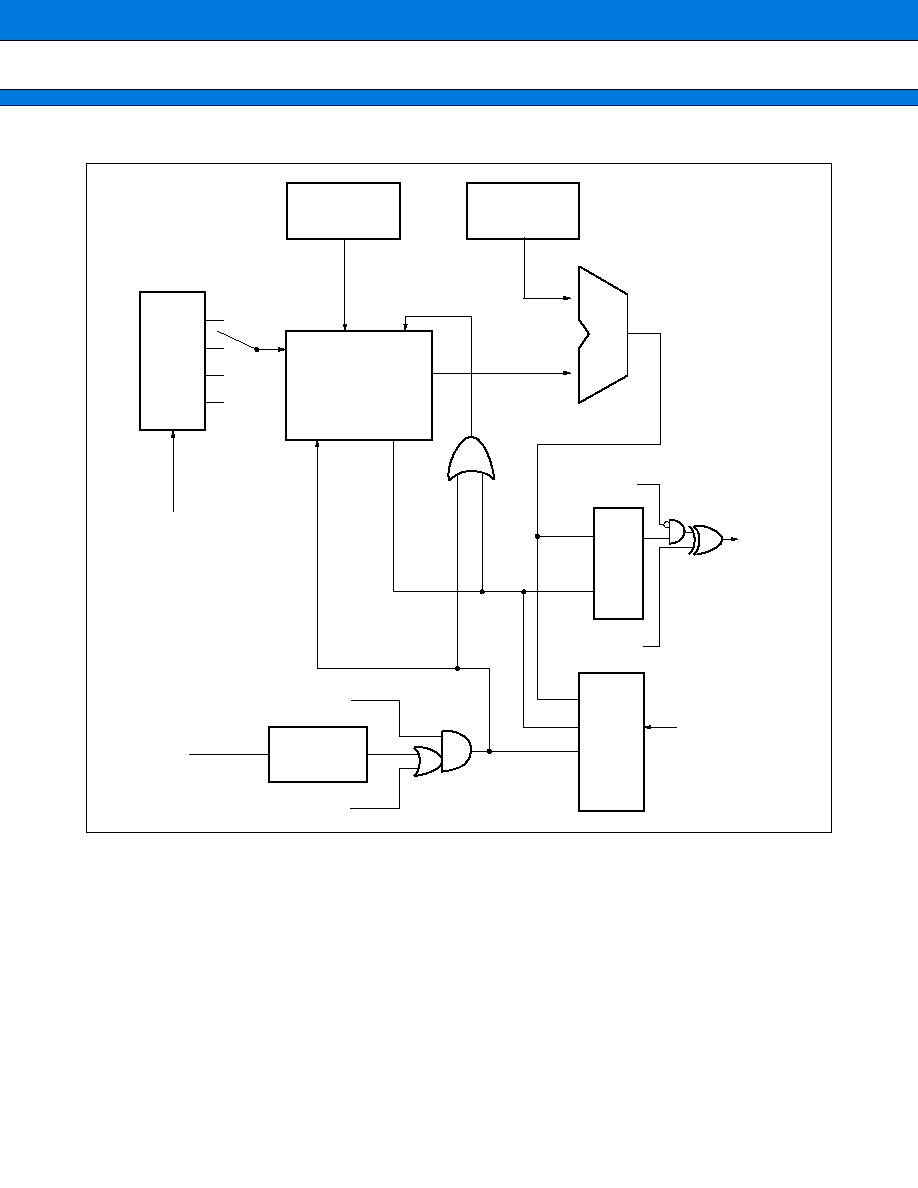
57
MB90220 Series
(2) Block Diagram
Prescaler
Oscillation clock
TRG input
Edge detection
Software trigger
Enable
IRQ
Reverse bit
PPG output
S Q
R
PPG mask
cmp
PDUT
PCSR
ck
Load
16-bit down-counter
Start
Borrow
1/1
1/4
1/16
1/64
Interrupt
selector
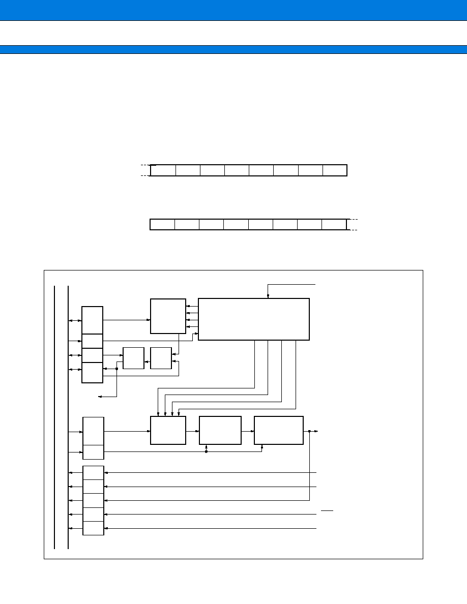
MB90220 Series
58
12. Watchdog Timer and Timebase Timer Functions
The watchdog timer consists of a 2-bit watchdog counter using carry from an 18-bit timebase timer as the clock
source, a control register, and a watchdog reset control section. The timebase timer consists of an 18-bit timer
and an interval interrupt control circuit.
(1) Register Configuration
(2) Block Diagram
0000A8
H
PONR
STBR
WRST
ERST
SRST
WTE
WT1
WT0
bit7
bit6
bit5
bit4
bit3
bit2
bit1
bit0
0000A9
H
(--)
(--)
(--)
(R/W)
(R/W)
(R)
(R/W)
(R/W)
--
--
--
TBIE
TBOF
TBR
TBC1
TBC0
bit15
bit14
bit13
bit12
bit11
bit10
bit9
bit8
WDTC
TBTC
XXXXXXXX
- - - XXXXX
Register name Address
Register name Address
Initial value
Initial value
(R)
(R)
(R)
(R)
(R)
(W)
(W)
(W)
∑ Watchdog Timer Control Register (WDTC)
∑ Timebase Timer Control Register (TBTC)
TBTC
TBC1
TBC0
TBR
TBIE
TBOF
Selector
AND
Q
R
S
Selector
Timebase
interrupt
WDTC
WT1
WT0
WTE
PONR
STBR
WRST
ERST
SRST
From RST bit of STBYC register
RST pin
From hardware standby controller
From power-on signal generator
WDGRST
To internal reset signal generator
2-bit counter
OF
CLR
Watchdog reset
signal generator
CLR
2
12
2
14
2
16
2
18
TBTRES
Clock input
Timebase timer
2
14
2
16
2
17
2
18
Oscillation clock
Internal data bus
59
MB90220 Series
13. Delay Interruupt Generation Module
The delayed interrupt generation module is used to generate an interrupt task switching. Using this module
allows an interrupt request to the F
2
MC-16F CPU to generated or cancel by software.
(1) Register Configuration
(2) Block Diagram
00009F
H
(--)
(--)
(--)
(--)
(--)
(--)
(--)
(R/W)
--
--
--
--
--
--
--
R0
bit15
bit14
bit13
bit12
bit11
bit10
bit9
bit8
DIRR
- - - - - - - 0
Register name Address
Initial value
∑ Delay Interrupt Source Generation/Cancel Register (DIRR)
Internal data bus
Source latch
Delay interrupt source generation/cancel decoder
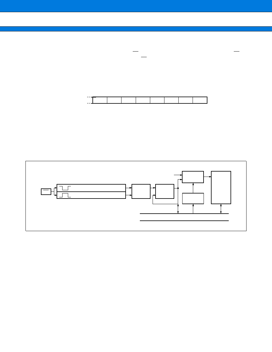
MB90220 Series
60
14. Write-inhibit RAM
The write-inhibit RAM is write-protectable with the WI pin input. Maintaining the "L" level input to the WI pin
prevents a certain area of RAM from being written. The WI pin has a 4-machine-cycle filter.
(1) Register Configuration
(2) Write-inhibit RAM Areas
Write-inhibit RAM areas:
000D00
H
to 000EFF
H
(MB90223)
001300
H
to 0014FF
H
(MB90224/P224A/P224B/W224A/W224B)
001500
H
to 0018FF
H
(MB90V220)
(3) Block Diagram
00008E
H
(--)
(--)
(--)
(R/W)
(--)
(--)
(--)
(--)
--
--
--
WI
--
--
--
--
bit7
bit6
bit5
bit4
bit3
bit2
bit1
bit0
WICR
- - - X - - - -
Register name Address
Initial value
∑ WI Control Register (WICR)
WI
4-machine cycle smoothing circuit
4-machine cycle smoothing circuit
S
R
Q
Priority
R
Q
Other area access
Write-inhibit
circuit
Write-inhibit
RAM
RAM
decoder
Select
Internal data bus
L
H
WR
S

61
MB90220 Series
15. Low-power Consumption Modes, Oscillation Stabilization Delay Time, and Gear Function
The MB90220 series has three low-power consumption modes: the sleep mode, the stop mode, the hardware
standby mode, and gear function.
Sleep mode is used to suspend only the CPU operation clock; the other components remain in operation. Stop
mode and hardware standby mode stop oscillation, minimizing the power consumption while holding data.
The gear function divides the external clock frequency, which is used usually as it is, to provide a lower machine
clock frequency. This function can therefore lower the overall operation speed without changing the oscillation
frequency. The function can select the machine clock as a division of the frequency of crystal oscillation or
external clock input by 1, 2, 4, or 16.
The OSC1 and OSC0 bits can be used to set the oscillation stabilization delay time for wake-up from stop mode
or hardware standby mode.
(1) Register Configuration
Note: The initial value (*) of bit0 to bit3 is changed by reset source.
0000A0
H
(W)
(W)
(R/W)
(R/W)
(R/W)
(R/W)
(R/W)
(R/W)
STP
SLP
SPL
RST
OSC1
OSC0
CLK1
CLK0
bit7
bit6
bit5
bit4
bit3
bit2
bit1
bit0
STBYC
0001* * * *
Register name Address
Initial value
∑ Standby Control Register (STBYC)
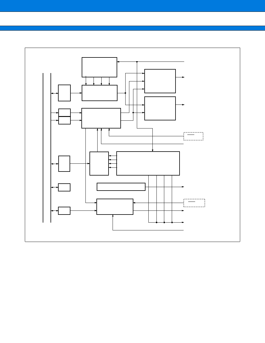
MB90220 Series
62
(2) Block Diagram
Selector
2
14
2
0
Selector
Gear divider
1/1 1/2 1/4 1/16
STBYC
CLK1
CLK0
SLP
STP
OSC1
OSC0
SPL
RST
Internal reset
signal generator
WDGRST
To watchdog timer
Internal RST
Standby controller
RST Release HST start
Pin high impedance controller
Pin Hi-Z
Interrupt request or RST
2
16
2
17
2
18
Clock input
Timebase timer
2
16
2
17
2
18
Peripheral clock
generator
CPU clock
generator
Peripheral clock
CPU clock
Oscillation clock
Internal data bus
HST pin
RST pin
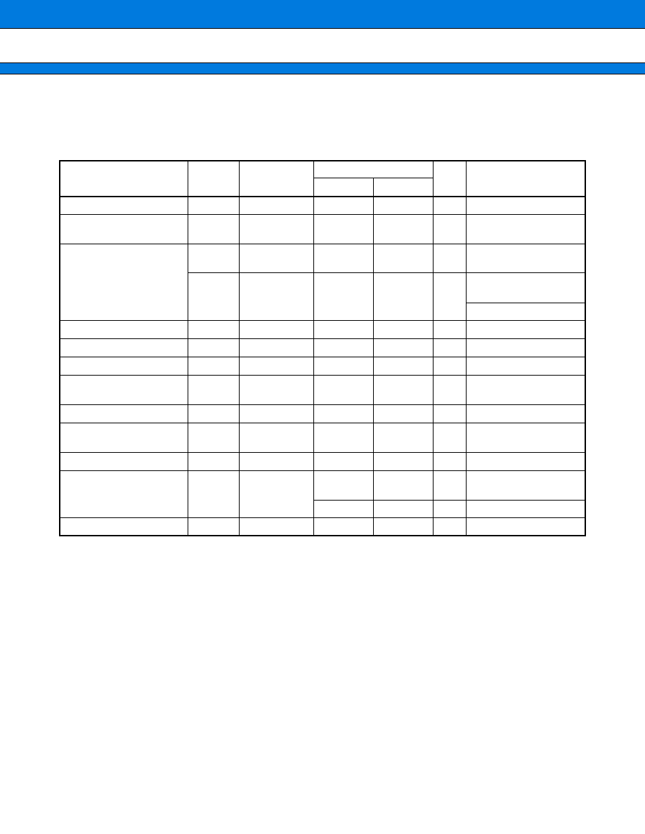
63
MB90220 Series
s
ELECTRICAL CHARACTERISTICS
1. Absolute Maximum Ratings
(V
SS
= AV
SS
= 0.0 V)
*1: V
1
must not exceed V
CC
+ 0.3 V.
*2: Output pins: P00 to P07, P10 to P17, P20 to P27, P30 to P37, P40 to P47, P50 to P57, P70 to P77, P80 to
P87, PA0 to PA7, PB0 to PB7, PC0 to PC5
*3: Output pins: P00 to P07, P10 to P17, P20 to P27, P30 to P37, P40 to P47, P50 to P57, P60 to P67, P70 to
P77, P80 to P87, P90 to P97, PA0 to PA7, PB0 to PB7, PC0 to PC5
WARNING:Semiconductor devices can be permanently damaged by application of stress (voltage, current,
temperature, etc.) in excess of absolute maximum ratings. Do not exceed these ratings.
Parameter
Symbol
Pin name
Value
Unit
Remarks
Min.
Max.
Power supply voltage
V
CC
V
CC
V
SS
≠ 0.3
V
SS
+ 7.0
V
Program voltage
V
PP
V
PP
V
SS
≠ 0.3
13.0
V
MB90P224A/P224B
MB90W224A/W224B
Analog power supply
voltage
AV
CC
AV
CC
V
SS
≠ 0.3
V
CC
+ 0.3
V
Power supply voltage
for A/D converter
AVRH
AVRL
AVRH
AVRL
V
SS
≠ 0.3
AV
CC
V
Reference voltage for
A/D converter
Input voltage
V
I
*
1
--
V
SS
≠ 0.3
V
CC
+ 0.3
V
Output voltage
V
O
*
2
V
SS
≠ 0.3
V
CC
+ 0.3
V
"L" level output current
I
OL
*
3
--
20
mA
Rush current
"L" level total output
current
I
OL
*
3
--
50
mA
Total output current
"H" level output current
I
OH
*
2
--
≠10
mA
Rush current
"H" level total output
current
I
OH
*
2
--
≠48
mA
Total output current
Power consumption
P
D
--
--
650
mW
Operating temperature
T
A
--
≠40
+105
∞
C
MB90223/224/P224B
/W224B
≠40
+85
∞
C
MB90P224A/W224A
Storage temperature
Tstg
--
≠55
+150
∞
C
MB90220 Series
64
2. Recommended Operating Condition
(V
SS
= AV
SS
= 0.0 V)
* : Excluding the temperature rise due to the heat produced.
WARNING:Recommended operating conditions are normal operating ranges for the semiconductor device. All the
device's electrical characteristics are warranted when operated within these ranges.
Always use semiconductor devices within the recommended operating conditions. Operation outside
these ranges may adversely affect reliability and could result in device failure.
No warranty is made with respect to uses, operating conditions, or combinations not represented on
the data sheet. Users considering application outside the listed conditions are advised to contact their
FUJITSU representative beforehand.
Parameter
Symbol
Pin
name
Value
Unit
Remarks
Min.
Max.
Power supply voltage
V
CC
V
CC
4.5
5.5
V
When operating
3.0
5.5
V
Retains the RAM state in
stop mode
Analog power supply
voltage
AV
CC
AV
CC
4.5
V
CC
+ 0.3
V
Power supply voltage for
A/D converter
AVRH
AVRH
AVRL
AV
CC
V
Reference voltage for A/D
converter
AVRL
AVRL
AV
SS
AVRH
V
Clock frequency
F
C
--
10
16
MHz
MB90224/P224A/W224A
MB90P224B/W224B
10
12
MHz
MB90223
Operating temperature
T
A
*
--
≠40
+105
∞
C
Single-chip mode
MB90223/224/P224B/
W224B
≠40
+85
∞
C
Single-chip mode
MB90P224A/W224A
≠40
+70
∞
C
External bus mode
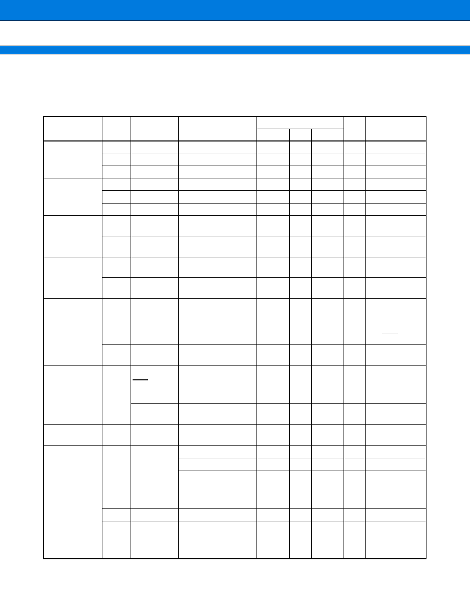
65
MB90220 Series
3. DC Characteristics
Single-chip mode
MB90223/224/P224B/W224B : (V
CC
= +4.5 V to +5.5 V, V
SS
= 0.0 V, T
A
= ≠40
∞
C to +105
∞
C)
MB90P224A/W224A
: (V
CC
= +4.5 V to +5.5 V, V
SS
= 0.0 V, T
A
= ≠40
∞
C to +85
∞
C)
External bus mode
: (V
CC
= +4.5 V to +5.5 V, V
SS
= 0.0 V, T
A
= ≠40
∞
C to +70
∞
C)
(Continued)
Parameter
Symbol
Pin name
Condition
Value
Unit
Remarks
Min.
Typ.
Max.
"H" level input
voltage
V
IH
X0
--
0.7 V
CC
--
V
CC
+ 0.3
V
CMOS level input
V
IHS
*
1
--
0.8 V
CC
--
V
CC
+ 0.3
V
Hysteresis input
V
IHM
MD0 to MD2
--
V
CC
≠ 0.3
--
V
CC
+ 0.3
V
"L" level input
voltage
V
IL
X0
--
V
SS
≠ 0.3
--
0.3 V
CC
V
CMOS level input
V
ILS
*
1
--
V
SS
≠ 0.3
--
0.2 V
CC
V
Hysteresis input
V
ILM
MD0 to MD2
--
V
SS
≠ 0.3
--
V
SS
+ 0.3
V
"H" level
output voltage
V
OH
*
2
V
CC
= 4.5 V
I
OH
= ≠4.0 mA
V
CC
≠ 0.5
--
V
CC
V
V
OH1
X1
V
CC
= 4.5 V
I
OH
= ≠2.0 mA
V
CC
≠ 2.5
--
V
CC
V
"L" level
output voltage
V
OL
*
3
V
CC
= 4.5 V
I
OL
= 4.0 mA
0
--
0.4
V
V
OL1
X1
V
CC
= 4.5 V
I
OL
= 2.0 mA
0
--
V
CC
≠ 2.5
V
Input leackage
current
I
I
*
1
V
CC
= 5.5 V
0.2 V
CC
< V
I
< 0.8 V
CC
--
--
±
10
µ
A
Hysteresis input
Except pins with
pull-up/pull-
down resistor
and RST pin
I
I2
X0
V
CC
= 5.5 V
0.2 V
CC
< V
I2
< 0.8 V
CC
--
--
±
20
µ
A
Pull-up resistor
R
pulU
RST
--
22
50
110
k
*
4
MB90223/224
MB90P224A/
W224A
MD1
--
22
50
150
k
*
4
MB90223/224
Pull-down
resistor
R
pulD
MD0
MD2
--
22
50
150
k
*
4
MB90223/224
Power supply
voltage*
8
I
CC
V
CC
F
C
= 12 MHz
--
70*
5
100
mA MB90223
F
C
= 16 MHz
--
70*
5
100
mA MB90224
F
C
= 16 MHz
--
90*
5
125
mA
MB90P224A/
P224B
MB90W224A/
W224B
I
CCS
V
CC
f
C
= 16 MHz*
9
--
--
60
mA At sleep mode
I
CCH
V
CC
--
--
5
10
µ
A
In stop mode
T
A
= +25
∞
C
At hardware
standby
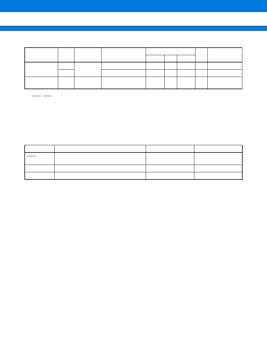
MB90220 Series
66
(Continued)
*1: Hysteresis input pins
RST, HST, P00 to P07, P10 to P17, P20 to P27, P30 to P37, P40 to P47, P50 to P57, P60 to P67, P80 to P87,
P90 to P97, PA0 to PA7, PB0 to PB7, PC0 to PC5
*2: Ouput pins
P00 to P07, P10 to P17, P20 to P27, P30 to P37, P40 to P47, P50 to P57, P70 to P77, P80 to P87, PA0 to
PA7, PB0 to PB7, PC0 to PC5
*3: Output pins
P00 to P07, P10 to P17, P20 to P27, P30 to P37, P40 to P47, P50 to P57, P60 to P67, P70 to P77, P80 to
P87, P90 to P97, PA0 to PA7, PB0 to PB7, PC0 to PC5
*4: A list of availabilities of pull-up/pull-down resistors
*5: V
CC
= +5.0 V, V
SS
= 0.0 V, T
A
= +25
∞
C, F
C
= 16 MHz
*6: The current value applies to the CPU stop mode with A/D converter inactive (V
CC
= AV
CC
= AVRH = +5.5 V).
*7: Other than V
CC
, V
SS
, AV
CC
and AV
SS
*8: Measurement condition of power supply current; external clock pin and output pin are open.
Measurement condition of V
CC
; see the table above mentioned.
*9: F
C
= 12 MHz for MB90223
Parameter
Symbol
Pin name
Condition
Value
Unit
Remarks
Min.
Typ.
Max.
Analog power
supply voltage
I
A
AV
CC
f
C
= 16 MHz*
9
--
3
7
mA
I
AH
--
--
--
5*
6
µ
A
At stop mode
Input
capacitance
C
IN
*
7
--
--
10
--
pF
Pin name
MB90223/224
MB90P224A/W224A
MB90P224B/W224B
RST
Availability of pull-up resistors is optionally
defined.
Pull-up resistors
available
Unavailable
MD1
Pull-up resistors available
Unavailable
Unavailable
MD0, MD2
Pull-up resistors available
Unavailable
Unavailable
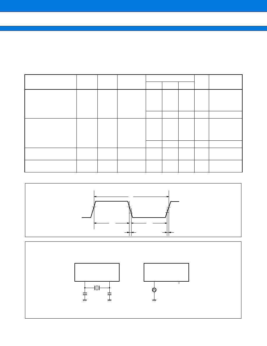
67
MB90220 Series
4. AC Characteristics
(1) Clock Timing Standards
Single-chip mode
MB90223/224/P224B/W224B : (V
CC
= +4.5 to +5.5 V, V
SS
= 0.0 V, T
A
= ≠40
∞
C to +105
∞
C)
MB90P224A/W224A
: (V
CC
= +4.5 to +5.5 V, V
SS
= 0.0 V, T
A
= ≠40
∞
C to +85
∞
C)
External bus mode
: (V
CC
= +4.5 to +5.5 V, V
SS
= 0.0 V, T
A
= ≠40
∞
C to +70
∞
C)
t
C
= 1/f
C
Parameter
Symbol
Pin
name
Condition
Value
Unit
Remarks
Min.
Typ.
Max.
Clock frequency
F
C
X0, X1
--
10
--
16
MHz
MB90224/
P224A/P224B
MB90W224A/
W224B
10
--
12
MHz
MB90223
Clock cycle time
t
C
X0, X1
--
62.5
--
100
ns
MB90224/
P224A/P224B
MB90W224A/
W224B
83.4
--
100
ns
MB90223
Input clock pulse width
P
WH
P
WL
X0
--
0.4 t
c
--
0.6 t
c
ns
Equivalent to
60% duty ratio
Input clock rising/falling
times
t
cr
t
cf
X0
--
--
--
8
ns
t
cr
+ t
cf
t
cf
t
cr
0.7 V
CC
0.3 V
CC
0.7 V
CC
0.7 V
CC
0.3 V
CC
P
WH
P
WL
t
c
∑ Clock Input Timings
When a crystal
or
ceramic resonator is used
When an external clock is used
Open
X0
X1
X0
X1
C
2
C
1
C
1
= C
2
= 10 pF
Select the optimum capacity value for the resonator
∑ Clock Conditions
MB90220 Series
68
V
CC
[V]
5.5
4.5
0
16
Fc
[MHz]
10
12
Single-chip mode
(MB90224/P224B/W224B)
(MB90223)
(MB90P224A/W224A)
External bus mode
: T
A
= ≠40
∞
C to +105
∞
C, Fc = 10 to 16 MHz
: T
A
= ≠40
∞
C to +105
∞
C, Fc = 10 to 12 MHz
: T
A
= ≠40
∞
C to +85
∞
C, Fc = 10 to 16 MHz
: T
A
= ≠40
∞
C to +70
∞
C, Fc = 10 to 16 MHz
(Fc = 10 to 12 MHz, only for MB90223)
Operation assurance range
∑ Relationship between Clock Frequency and Supply Voltage
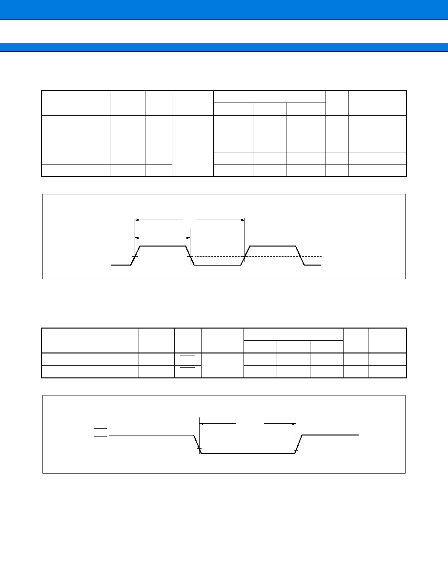
69
MB90220 Series
(2) Clock Output Timing
(External bus mode: V
CC
= +4.5 V to +5.5 V, V
SS
= 0.0 V, T
A
= ≠40
∞
C to +70
∞
C)
t
CYC
= n/F
C
, n gear ratio (1, 2, 4, 16)
(3) Reset and Hardware Standby Input Standards
Single-chip
mode
MB90223/224/P224B/W224B:
(V
CC
= +4.5 V to +5.5 V, V
SS
= 0.0 V, T
A
= ≠40
∞
C to +105
∞
C)
MB90P224A/W224A
: (V
CC
= +4.5 V to +5.5 V, V
SS
= 0.0 V, T
A
= ≠40
∞
C to +85
∞
C)
External bus mode
: (V
CC
= +4.5 V to +5.5 V, V
SS
= 0.0 V, T
A
= ≠40
∞
C to +70
∞
C)
*: The machine cycle time (t
CYC
) at hardware standby is set to 1/16 divided oscillation.
Parameter
Symbol
Pin
name
Condition
Value
Unit
Remarks
Min.
Typ.
Max.
Machine cycle time
t
CYC
CLK
Load
condition:
80 pF
62.5
--
1600
ns
MB90224/
P224A/P224B
MB90W224A/
224B
83.4
--
1600
ns
MB90223
CLK
CLK
t
CHCL
CLK
t
CYC
/2 ≠ 20
--
t
CYC
/2
ns
Parameter
Symbol
Pin
name
Condition
Value
Unit
Remarks
Min.
Typ.
Max.
Reset input time
t
RSTL
RST
--
5 t
CYC
--
--
ns
Hardware standby input time
t
HSTL
HST
5 t
CYC
--
--
ns
*
CLK
1/2 V
CC
t
CYC
t
CHCL
RST
HST
0.2 V
CC
0.2 V
CC
t
RSTL
, t
HSTL
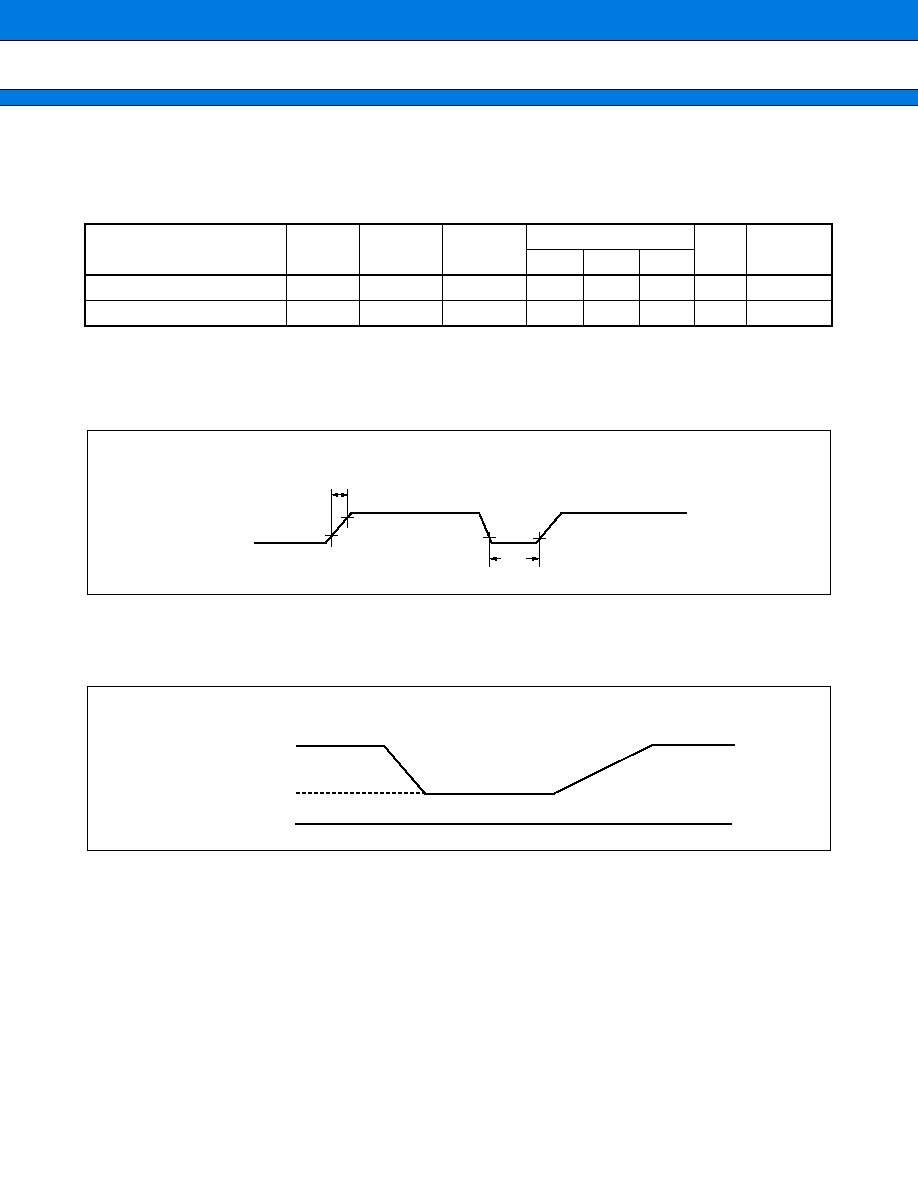
MB90220 Series
70
(4) Power on Supply Specifications (Power-on Reset)
Single-chip
mode
MB90223/224/P224B/W224B:
(V
CC
= +4.5 V to +5.5 V, V
SS
= 0.0 V, T
A
= ≠40
∞
C to +105
∞
C)
MB90P224A/W224A
: (V
CC
= +4.5 V to +5.5 V, V
SS
= 0.0 V, T
A
= ≠40
∞
C to +85
∞
C)
External bus mode
: (V
CC
= +4.5 V to +5.5 V, V
SS
= 0.0 V, T
A
= ≠40
∞
C to +70
∞
C)
* : Before power supply rising, it is required to be V
CC
< 0.2 V.
Notes: ∑ Power-on reset assumes the above values.
∑ Whether the power-on reset is required or not, turn the power on according to these characteristics and
trigger the power-on reset.
∑ There are internal registers (STBYC, etc.) which is initialized only by the power-on reset in the device.
Note: Note on changing power supply
Even if above characteristics are not insufficient, abrupt changes in power supply voltage may cause a power-
on reset. Therefore, at the time of a momentary changes such as when power is turned on, rise the power
smoothly as shown below.
Parameter
Symbol
Pin name
Condition
Value
Unit
Remarks
Min.
Typ.
Max.
Power supply rising time
t
R
V
CC
--
--
--
30
ms
*
Power supply cut-off time
t
OFF
V
CC
--
1
--
--
ms
V
CC
t
R
4.5 V
0.2 V
t
OFF
0.2 V
CC
0.2 V
CC
∑ Power-on Reset
Main power supply voltage
This rising edge should be
50 mV/ms or less
Subpower supply voltage
Vss
∑ Changing Power Supply
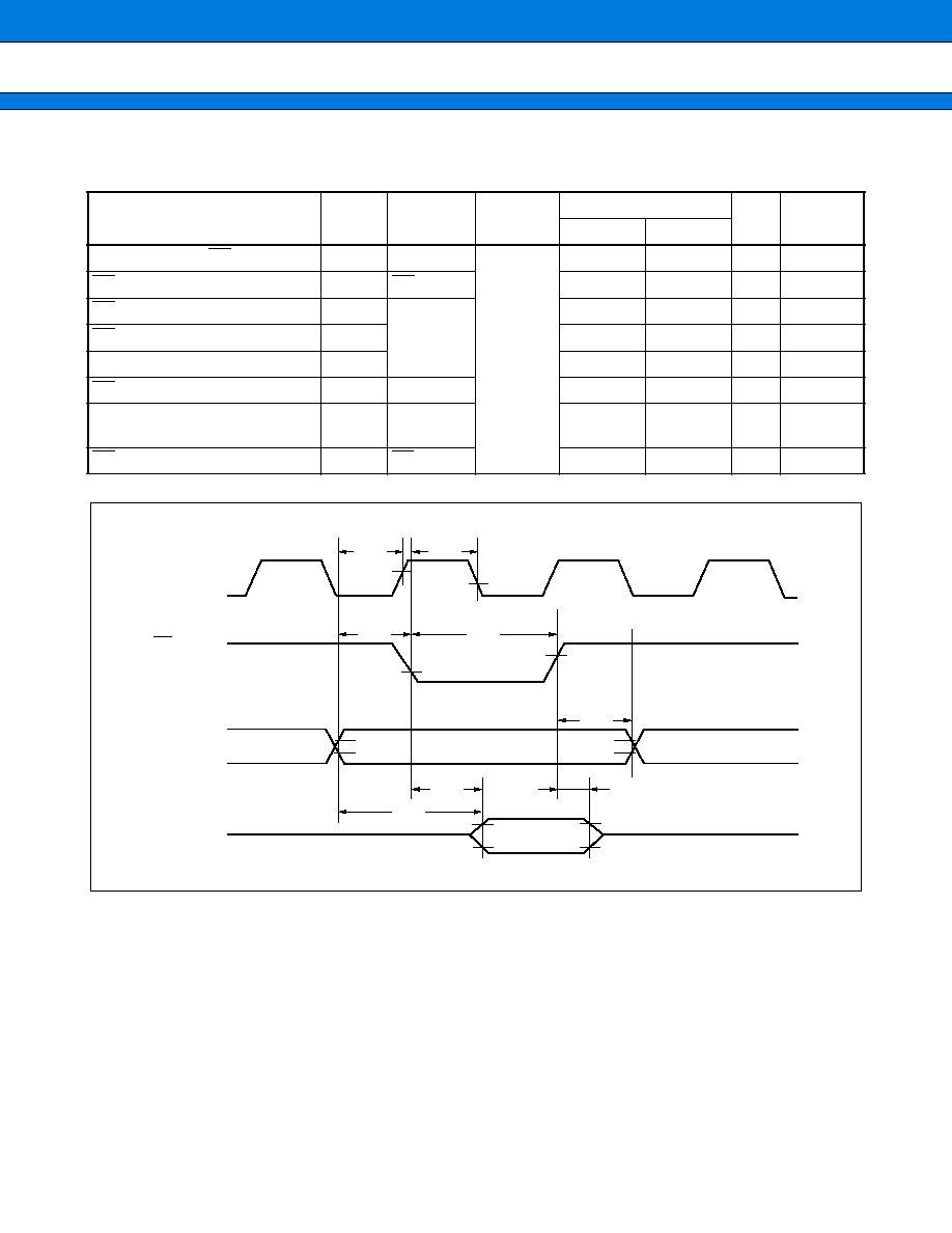
71
MB90220 Series
(5) Bus Read Timing
(V
CC
= +4.5 V to +5.5 V, V
SS
= 0.0 V, T
A
= ≠40
∞
C to +70
∞
C)
Parameter
Symbol
Pin name
Condition
Value
Unit
Remarks
Min.
Max.
Valid address
RD
time
t
AVRL
A23 to A00
Load
condition:
80 pF
t
CYC
/2 ≠ 20
--
ns
RD pulse width
t
RLRH
RD
t
CYC
≠ 25
--
ns
RD
Valid data input
t
RLDV
D15 to D00
--
t
CYC
≠ 30
ns
RD
Data hold time
t
RHDX
0
--
ns
Valid address
Valid data input t
AVDV
--
3 t
CYC
/2 ≠ 40
ns
RD
Address valid time
t
RHAX
A23 to A00
t
CYC
/2 ≠ 20
--
ns
Valid address
CLK
time
t
AVCH
A23 to A00
CLK
t
CYC
/2 ≠ 25
--
ns
RD
CLK
time
t
RLCL
RD, CLK
t
CYC
/2 ≠ 25
--
ns
CLK
RD
A23 to A00
D15 to D00
t
RHDX
Read data
0.8 V
CC
0.2 V
CC
0.8 V
CC
0.2 V
CC
0.7 V
CC
0.3 V
CC
0.3 V
CC
0.7 V
CC
0.7 V
CC
0.3 V
CC
0.7 V
CC
0.3 V
CC
t
AVCH
t
RLCL
t
AVRL
t
RLRH
t
RHAX
t
RLDV
t
AVDV
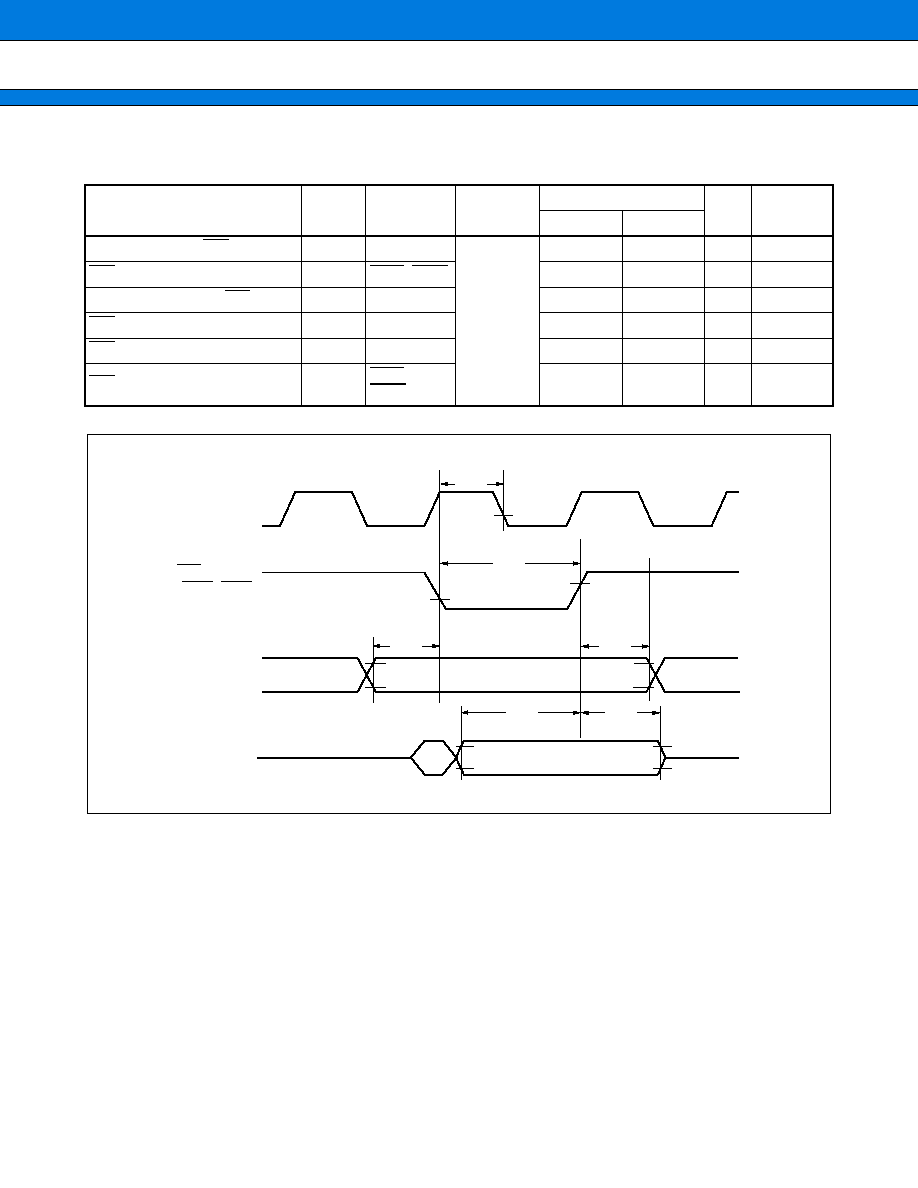
MB90220 Series
72
(6) Bus Write Timing
(V
CC
= +4.5 V to +5.5 V, V
SS
= 0.0 V, T
A
= ≠40
∞
C to +70
∞
C)
Parameter
Symbol
Pin name
Condition
Value
Unit
Remarks
Min.
Max.
Valid address
WR
time
t
AVWL
A23 to A00
Load
condition:
80 pF
t
CYC
/2 ≠ 20
--
ns
WR pulse width
t
WLWH
WRL, WRH
t
CYC
≠ 25
--
ns
Valid data output
WR
time t
DVWH
D15 to D00
t
CYC
≠ 40
--
ns
WR
Data hold time
t
WHDX
D15 to D00
t
CYC
/2 ≠ 20
--
ns
WR
Address valid time
t
WHAX
A23 to A00
t
CYC
/2 ≠ 20
--
ns
WR
CLK
time
t
WLCL
WRL,
WRH, CLK
t
CYC
/2 ≠ 25
--
ns
CLK
WR
(WRL, WRH)
A23 to A00
D15 to D00
Read data
0.3 V
CC
0.3 V
CC
0.7 V
CC
0.7 V
CC
0.3 V
CC
0.7 V
CC
0.3 V
CC
0.3 V
CC
0.7 V
CC
0.3 V
CC
0.7 V
CC
Indeter-
minate
t
WLCL
t
WLWH
t
AVWL
t
WHAX
t
WHDX
t
DVWH
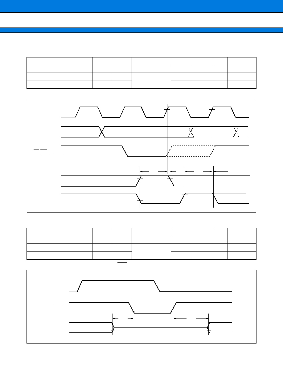
73
MB90220 Series
(7) Ready Input Timing
(V
CC
= +4.5 V to +5.5 V, V
SS
= 0.0 V, T
A
= ≠40
∞
C to +70
∞
C)
Note: Use the auto-ready function if the RDY setup time is insufficient.
(8) Hold Timing
(V
CC
= +4.5 V to +5.5 V, V
SS
= 0.0 V, T
A
= ≠40
∞
C to +70
∞
C)
Note: It takes at least one machine cycle for HAK to vary after HRQ is fetched.
Parameter
Symbol
Pin
name
Condition
Value
Unit
Remarks
Min.
Max.
RDY setup time
t
RYHS
RDY
Load condition:
80 pF
40
--
ns
RDY hold time
t
RYHH
RDY
0
--
ns
Parameter
Symbol
Pin
name
Condition
Value
Unit
Remarks
Min.
Max.
Pin floating
HAK
time
t
XHAL
HAK
Load condition:
80 pF
30
t
CYC
ns
HAK
time
pin valid time
t
HAHV
HAK
t
CYC
2 t
CYC
ns
A23 to A00
CLK
RD/WR
(WRL, WRH)
RDY
No wait
One wait
t
RYHH
t
RYHH
0.8 V
CC
0.8 V
CC
0.2 V
CC
0.8 V
CC
0.8 V
CC
0.7 V
CC
0.7 V
CC
t
RYHS
t
RYHS
HRQ
HAK
Each pin
High impedance
0.3 V
CC
0.7 V
CC
0.2 V
CC
0.8 V
CC
t
XHAL
t
HAHV
MB90220 Series
74
(9) UART Timing
Single-chip
mode
MB90223/224/P224B/W224B:
(V
CC
= +4.5 V to +5.5 V, V
SS
= 0.0 V, T
A
= ≠40
∞
C to +105
∞
C)
MB90P224A/W224A
: (V
CC
= +4.5 V to +5.5 V, V
SS
= 0.0 V, T
A
= ≠40
∞
C to +85
∞
C)
External bus mode
: (V
CC
= +4.5 V to +5.5 V, V
SS
= 0.0 V, T
A
= ≠40
∞
C to +70
∞
C)
Notes: ∑ These AC characteristics assume in CLK synchronization mode.
∑ "t
CYC
" is the machine cycle (unit: ns).
Parameter
Symbol
Pin
name
Condition
Value
Unit
Remarks
Min.
Max.
Serial clock cycle time
t
SCYC
--
Load condition:
80 pF
8 t
CYC
--
ns
Internal
clock
operation
output pin
SCLK
SOUT delay time
t
SLOV
--
≠80
80
ns
Valid SIN
SCLK
t
IVSH
--
100
--
ns
SCLK
Valid SIN hold time t
SHIX
--
60
--
ns
Serial clock "H" pulse width
t
SHSL
--
Load condition:
80 pF
4 t
CYC
--
ns
External
clock
operation
output pin
Serial clock "L" pulse width
t
SLSH
--
4 t
CYC
--
ns
SCLK
SOUT delay time
t
SLOV
--
--
150
ns
Valid SIN
SCLK
t
IVSH
--
60
--
ns
SCLK
valid SIN hold time t
SHIX
--
60
--
ns
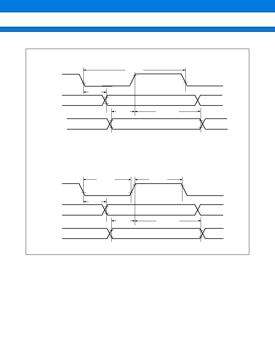
75
MB90220 Series
SOD
SCK
SID
t
SLOV
t
SCYC
t
IVSH
t
SHIX
SOD
SCK
SID
t
SLOV
t
SLSH
t
IVSH
t
SHIX
t
SHSL
0.3 V
CC
0.3 V
CC
0.7 V
CC
0.7 V
CC
0.3 V
CC
0.8 V
CC
0.2 V
CC
0.8 V
CC
0.2 V
CC
0.2 V
CC
0.2 V
CC
0.8 V
CC
0.8 V
CC
0.7 V
CC
0.3 V
CC
0.8 V
CC
0.2 V
CC
0.8 V
CC
0.2 V
CC
∑ Internal Shift Clock Mode
∑ External Shift Clock Input Mode
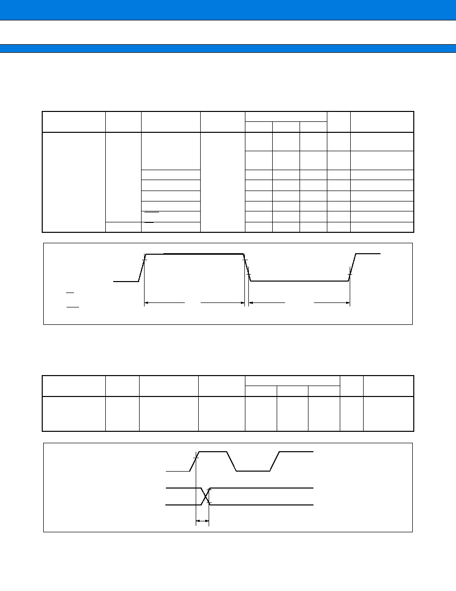
MB90220 Series
76
(10) Resourse Input Timing
Single-chip mode
MB90223/224/P224B/W224B: (V
CC
= +4.5 V to +5.5 V, V
SS
= 0.0 V, T
A
= ≠40
∞
C to +105
∞
C)
MB90P224A/W224A
: (V
CC
= +4.5 V to +5.5 V, V
SS
= 0.0 V, T
A
= ≠40
∞
C to +85
∞
C)
External bus mode
: (V
CC
= +4.5 V to +5.5 V, V
SS
= 0.0 V, T
A
= ≠40
∞
C to +70
∞
C)
(11) Resourse Output Timing
Single-chip mode
MB90223/224/P224B/W224B: (V
CC
= +4.5 V to +5.5 V, V
SS
= 0.0 V, T
A
= ≠40
∞
C to +105
∞
C)
MB90P224A/W224A
: (V
CC
= +4.5 V to +5.5 V, V
SS
= 0.0 V, T
A
= ≠40
∞
C to +85
∞
C)
External bus mode
: (V
CC
= +4.5 V to +5.5 V, V
SS
= 0.0 V, T
A
= ≠40
∞
C to +70
∞
C)
Parameter
Symbol
Pin name
Condition
Value
Unit
Remarks
Min.
Typ.
Max.
Input pulse width
t
TIWH
t
TIWL
TIN1 to TIN5
Load
condition:
80 pF
4 t
CYC
--
--
ns
External event
count input mode
2 t
CYC
--
--
ns
Trigger input/gate
input mode
PWC0 to PWC3
2 t
CYC
--
--
ns
ASR0 to ASR3
2 t
CYC
--
--
ns
INT0 to INT7
3 t
CYC
--
--
ns
TRG0
2 t
CYC
--
--
ns
ATG
2 t
CYC
--
--
ns
t
WIWL
WI
4 t
CYC
--
--
ns
Parameter
Symbol
Pin name
Condition
Value
Unit
Remarks
Min.
Typ.
Max.
CLK
T
OUT
transition time
t
TO
TOT0 to TOT5
PPG0 to PPG1
POT0 to POT3
DOT0 to DOT7
Load
condition:
80 pF
--
--
30
ns
0.8 V
CC
0.8 V
CC
0.2 V
CC
0.2 V
CC
TIN1 to TIN5
PWC0 to PWC3
ASR0 to ASR3
INT0 to INT7
WI
TRG0
ATG
t
TIWH
t
TIWL
, t
WIWL
CLK
T
OUT
t
TO
0.7 V
CC
0.7 V
CC
0.3 V
CC
77
MB90220 Series
5. A/D Converter Electrical Characteristics
Single-chip mode MB90223/224/P224B/W224B
: (AV
CC
= V
CC
= +4.5 V to +5.5 V, AV
SS
=V
SS
= 0.0 V, T
A
= ≠40
∞
C to +105
∞
C, +4.5 V
AVRH ≠ AVRL)
MB90P224A/W224A
: (AV
CC
= V
CC
= +4.5 V to +5.5 V, AV
SS
= V
SS
=0.0 V, T
A
= ≠40
∞
C to +85
∞
C, +4.5 V
AVRH ≠ AVRL)
External bus mode
: (AV
CC
= V
CC
= +4.5 V to +5.5 V, AV
SS
= V
SS
=0.0 V, T
A
= ≠40
∞
C to +70
∞
C, +4.5 V
AVRH ≠ AVRL)
*1: These standards in this table are for MB90224/P224A/P224B/W224A/W224B.
MB90223: Minimum conversion time is 8.17
µ
s and minimum sampling time is 5
µ
s at t
CYC
= 83.4 ns.
*2: The current value applies to the CPU stop mode with the A/D converter inactive (V
CC
= AV
CC
= AVRH = +5.5 V).
Notes: (1) The error becomes larger as | AVRH ≠ AVRL | becomes smaller.
(2) Use the output impedance of the external circuit for analog input under the following conditions:
External circuit output impedance < approx. 10 k
(Sampling time approx. 3.75
µ
s, t
CYC
= 62.5 ns)
(3) Precision values are standard values applicable to sleep mode.
(4) If V
CC
/AV
CC
or V
SS
/AV
SS
is caused by a noise to drop to below the analog input volgtage, the analog
input current is likely to increase. In such cases, a bypass capacitor or the like should be provided in
the external circuit to suppress the noise.
Parameter
Symbol
Pin
name
Condition
Value
Unit
Remarks
Min.
Typ.
Max.
Resolution n
--
--
--
--
10
bit
Total error
--
--
--
--
--
±3.0
LSB
Linearity error
--
--
--
--
--
±2.0
LSB
Differential linearity error
--
--
--
--
--
±1.5
LSB
Zero transition voltage
V
0T
AN00 to
AN15
--
AVRL ≠ 1.5 AVRL + 0.5 AVRL + 2.5
LSB
Full-scale transition
voltage
V
FST
--
AVRH ≠ 3.5 AVRH ≠ 1.5 AVRH + 0.5
LSB
Conversion time*
1
T
CONV
--
t
CYC
= 62.5 ns
6.125
--
--
µ
s
98 machine
cycles
Sampling period
T
SAMP
--
3.75
--
--
µ
s
60 machine
cycles
Analog port input current
I
AIN
AN00 to
AN15
--
--
--
±
0.1
µ
A
Analog input voltage
V
AIN
--
AVRL
--
AVRH
V
Analog reference voltage
--
AVRH
--
AVRL
--
AV
CC
V
AVRL
--
AV
SS
--
AVRH
V
Reference voltage supply
current
I
R
AVRH
--
--
200
500
µ
A
I
RH
--
--
--
5*
2
µ
A
Variation between
channels
--
AN00 to
AN15
--
--
--
4
LSB
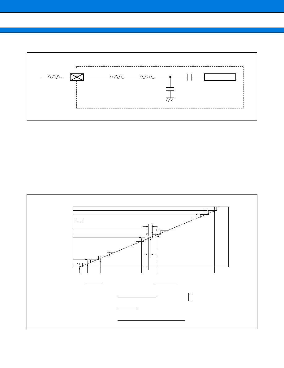
MB90220 Series
78
6. A/D Converter Glossary
Resolution:
Analog changes that are identifiable with the A/D converter
When the number of bits is 10, analog voltage can be divided into 2
10
= 1024.
Total error:
Difference between actual and logical values. This error is caused by a zero transition
error, full-scale transition error, linearity error, differential linearity error, or by noise.
Linearity error:
The deviation of the straight line connecting the zero transition point ("00 0000 0000"
"00 0000 0001") with the full-scale transition point ("11 1111 1111"
"11 1111
1110") from actual conversion characteristics
Differential linearity error: The deviation of input voltage needed to change the output code by 1 LSB from the
theoretical value
Note: The values shown here are reference values.
Analog input
Comparator
C
1
C
0
R
ON2
R
ON1
R
ON1
: Approx. 1.5 k
R
ON2
: Approx. 1.5 k
C
0
: Approx. 60 pF
C
1
: Approx. 4 pF
∑ Analog Input Circuit Mode
V
FST
V
NT
V
0T
1 LSB
V
FST
≠ V
0T
1022
=
Linearity error
V
NT
≠ (N
◊
1 LSB + V
0T
)
=
1 LSB
Differential linearity error
V
NT
≠ V
(N≠1)T
=
1 LSB
Total error
Digital output
11 1111 1111
11 1111 1110
11 1111 1101
00 0000 0010
00 0000 0001
00 0000 0000
≠ 1
V
(N + 1)T
N = 0 to 1022
V
NT (N = 0)
= V
0T
V
NT (N = 1022)
= V
FST
N = 1 to 1022
∑
∑
∑
∑
N + 1
N
N ≠ 1
Linearity error
N
◊
1LSB + V
0T
V
(N ≠ 1)T
V
1T
V
2T
Theoretical value (V
NT
)
Theoretical value
Actual conversion value
AVRL
AVRH (V)
∑
∑
∑
∑
∑
, 1 LSB theoretical value
AVRH
≠ AVRL
1022
=
Total error
V
NT
≠ {(N + 0.5)
◊
1 LSB theoretical value}
=
1 LSB theoretical value
N = 0 to 1022
79
MB90220 Series
s
EXAMPLE CHARACTERISTICS
(1) Power Supply Current
Note: These are not assured value of characteristics but example characteristics.
(2) Output Voltage
Note: These are not assured value of characteristics but example characteristics.
120
110
100
90
80
70
60
50
40
≠50
0
50
100
150
40
30
20
10
0
≠10
≠50
0
50
100
150
T
A
(
∞
C)
I
CC
(mA)
I
CCH
(
µ
A)
T
A
(
∞
C)
I
CC
vs. T
A
example characteristics
I
CCH
vs.
T
A
example characteristics
Fc = 16 MHz
External clock input
V
CC
= 5.0 V
MB90P224A
MB90223
V
CC
= 5 V
5.5
5.0
4.0
4.5
3.5
3.0
≠15
≠10
≠5
0
5
V
OH
(V)
I
OL
(mA)
V
OH
vs.
I
OH
example characteristics
2.0
1.5
0.5
1.0
0.0
≠0.5
V
OL
(V)
I
OH
(mA)
V
OL
vs.
I
OL
example characteristics
≠5
0
5
10
15
20
25
T
A
= +25
∞
C
V
CC
=
5.0 V
T
A
= +25
∞
C
V
CC
=
5.0 V
MB90220 Series
80
(3) Pull-up/Pull-down Resistor
Note: These are not assured value of characteristics but example characteristics.
(4) Analog Filter
Note: These are not assured value of characteristics but example characteristics.
100
90
80
70
60
50
40
30
20
≠50
0
50
100
150
≠50
0
50
100
150
T
A
(
∞
C)
R
pulD
(k
)
R
pulU
(k
)
T
A
(
∞
C)
Pull-down resistor example characteristics
Pull-up resistor example characteristics
V
CC
= 4.5 V
V
CC
= 5.0 V
V
CC
= 5.5 V
V
CC
= 4.5 V
V
CC
= 5.0 V
V
CC
= 5.5 V
100
90
80
70
60
50
40
30
20
80
70
60
50
40
30
4.0
4.5
5.0
5.5
6.0
Input pulse width (ns)
Analog filter example characteristics
V
CC
(V)
20
10
Filtering enable
T
A
= +25
∞
C
81
MB90220 Series
s
INSTRUCTION SET (412 INSTRUCTIONS)
Table 1 Explanation of Items in Table of Instructions
Item
Explanation
Mnemonic
Upper-case letters and symbols: Represented as they appear in assembler
Lower-case letters: Replaced when described in assembler.
Numbers after lower-case letters: Indicate the bit width within the instruction.
#
Indicates the number of bytes.
~
Indicates the number of cycles.
See Table 4 for details about meanings of letters in items.
B
Indicates the correction value for calculating the number of actual cycles during
execution of instruction.
The number of actual cycles during execution of instruction is summed with the value in
the "cycles" column.
Operation
Indicates operation of instruction.
LH
Indicates special operations involving the bits 15 through 08 of the accumulator.
Z: Transfers "0".
X: Extends before transferring.
--: Transfers nothing.
AH
Indicates special operations involving the high-order 16 bits in the accumulator.
*: Transfers from AL to AH.
--: No transfer.
Z: Transfers 00
H
to AH.
X: Transfers 00
H
or FF
H
to AH by extending AL.
I
Indicates the status of each of the following flags: I (interrupt enable), S (stack), T (sticky
bit), N (negative), Z (zero), V (overflow), and C (carry).
*: Changes due to execution of instruction.
--: No change.
S: Set by execution of instruction.
R: Reset by execution of instruction.
S
T
N
Z
V
C
RMW
Indicates whether the instruction is a read-modify-write instruction (a single instruction
that reads data from memory, etc., processes the data, and then writes the result to
memory.).
*: Instruction is a read-modify-write instruction
--: Instruction is not a read-modify-write instruction
Note: Cannot be used for addresses that have different meanings depending on
whether they are read or written.

MB90220 Series
82
Table 2 Explanation of Symbols in Table of Instructions
(Continued)
Symbol
Explanation
A
32-bit accumulator
The number of bits used varies according to the instruction.
Byte: Low order 8 bits of AL
Word: 16 bits of AL
Long: 32 bits of AL, AH
AH
High-order 16 bits of A
AL
Low-order 16 bits of A
SP
Stack pointer (USP or SSP)
PC
Program counter
SPCU
Stack pointer upper limit register
SPCL
Stack pointer lower limit register
PCB
Program bank register
DTB
Data bank register
ADB
Additional data bank register
SSB
System stack bank register
USB
User stack bank register
SPB
Current stack bank register (SSB or USB)
DPR
Direct page register
brg1
DTB, ADB, SSB, USB, DPR, PCB, SPB
brg2
DTB, ADB, SSB, USB, DPR, SPB
Ri
R0, R1, R2, R3, R4, R5, R6, R7
RWi
RW0, RW1, RW2, RW3, RW4, RW5, RW6, RW7
RWj
RW0, RW1, RW2, RW3
RLi
RL0, RL1, RL2, RL3
dir
addr16
addr24
addr24 0 to 15
addr24 16 to 23
Compact direct addressing
Direct addressing
Physical direct addressing
Bits 0 to 15 of addr24
Bits 16 to 23 of addr24
io
I/O area (000000
H
to 0000FF
H
)
83
MB90220 Series
(Continued)
Symbol
Explanation
#imm4
#imm8
#imm16
#imm32
ext (imm8)
4-bit immediate data
8-bit immediate data
16-bit immediate data
32-bit immediate data
16-bit data signed and extended from 8-bit immediate data
disp8
disp16
8-bit displacement
16-bit displacement
bp
Bit offset value
vct4
vct8
Vector number (0 to 15)
Vector number (0 to 255)
( )b
Bit address
rel
ear
eam
Branch specification relative to PC
Effective addressing (codes 00 to 07)
Effective addressing (codes 08 to 1F)
rlst
Register list

MB90220 Series
84
Table 3 Effective Address Fields
* : The number of bytes for address extension is indicated by the "+" symbol in the "#" (number of bytes) column in
the Table of Instructions.
Code
Notation
Address format
Number of bytes in
address extemsion*
00
01
02
03
04
05
06
07
R0
R1
R2
R3
R4
R5
R6
R7
RW0
RW1
RW2
RW3
RW4
RW5
RW6
RW7
RL0
(RL0)
RL1
(RL1)
RL2
(RL2)
RL3
(RL3)
Register direct
"ea" corresponds to byte, word, and
long-word types, starting from the
left
--
08
09
0A
0B
@RW0
@RW1
@RW2
@RW3
Register indirect
0
0C
0D
0E
0F
@RW0 +
@RW1 +
@RW2 +
@RW3 +
Register indirect with post-increment
0
10
11
12
13
14
15
16
17
@RW0 + disp8
@RW1 + disp8
@RW2 + disp8
@RW3 + disp8
@RW4 + disp8
@RW5 + disp8
@RW6 + disp8
@RW7 + disp8
Register indirect with 8-bit
displacement
1
18
19
1A
1B
@RW0 + disp16
@RW1 + disp16
@RW2 + disp16
@RW3 + disp16
Register indirect with 16-bit
displacemen
2
1C
1D
1E
1F
@RW0 + RW7
@RW1 + RW7
@PC + dip16
addr16
Register indirect with index
Register indirect with index
PC indirect with 16-bit displacement
Direct address
0
0
2
2
85
MB90220 Series
Table 4 Number of Execution Cycles for Each Form of Addressing
* : "(a)" is used in the "cycles" (number of cycles) column and column B (correction value) in the Table of Instructions.
Table 5 Correction Values for Number of Cycles Used to Calculate Number of Actual Cycles
* : "(b)", "(c)", and "(d)" are used in the "cycles" (number of cycles) column and column B (correction value) in the
Table of Instructions.
Code
Operand
(a)*
Number of execution cycles for each from of addressing
00 to 07
Ri
RWi
RLi
Listed in Table of Instructions
08 to 0B
@RWj
1
0C to 0F
@RWj +
4
10 to 17
@RWi + disp8
1
18 to 1B
@RWj + disp16
1
1C
1D
1E
1F
@RW0 + RW7
@RW1 + RW7
@PC + dip16
@addr16
2
2
2
1
Operand
(b)*
(c)*
(d)*
byte
word
long
Internal register
+
0
+
0
+
0
Internal RAM even address
+
0
+
0
+
0
Internal RAM odd address
+
0
+
1
+
2
Even address not in internal RAM
+
1
+
1
+
2
Odd address not in internal RAM
+
1
+
3
+
6
External data bus (8 bits)
+
1
+
3
+
6
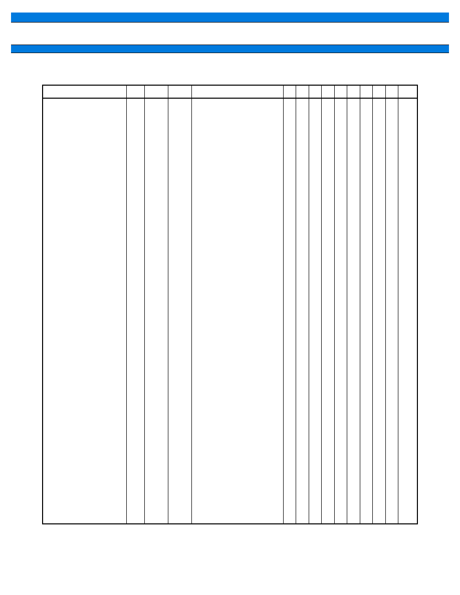
MB90220 Series
86
Table 6 Transfer Instructions (Byte) [50 Instructions]
(Continued)
Mnemonic
#
cycles
B
Operation
LH AH
I
S
T
N
Z
V
C
RMW
MOV
A, dir
MOV
A, addr16
MOV
A, Ri
MOV
A, ear
MOV
A, eam
MOV
A, io
MOV
A, #imm8
MOV
A, @A
MOV
A, @RLi+disp8
MOV
A, @SP+disp8
MOVP
A, addr24
MOVP
A, @A
MOVN A, #imm4
MOVX
A, dir
MOVX
A, addr16
MOVX
A, Ri
MOVX
A, ear
MOVX
A, eam
MOVX
A, io
MOVX
A, #imm8
MOVX
A, @A
MOVX
A,@RWi+disp8
MOVX
A, @RLi+disp8
MOVX
A, @SP+disp8
MOVPX A, addr24
MOVPX A, @A
MOV
dir, A
MOV
addr16, A
MOV
Ri, A
MOV
ear, A
MOV
eam, A
MOV
io, A
MOV
@RLi+disp8, A
MOV
@SP+disp8, A
MOVP
addr24, A
MOV
Ri, ear
MOV
Ri, eam
MOVP
@A, Ri
MOV
ear, Ri
MOV
eam, Ri
MOV
Ri, #imm8
MOV
io, #imm8
MOV
dir, #imm8
MOV
ear, #imm8
MOV
eam, #imm8
MOV
@AL, AH
2
3
1
2
2+
2
2
2
3
3
5
2
1
2
3
2
2
2+
2
2
2
2
3
3
5
2
2
3
1
2
2+
2
3
3
5
2
2+
2
2
2+
2
3
3
3
3+
2
2
2
1
1
2+ (a)
2
2
2
6
3
3
2
1
2
2
1
1
2+ (a)
2
2
2
3
6
3
3
2
2
2
1
2
2+ (a)
2
6
3
3
2
3+ (a)
3
3
3+ (a)
2
3
3
2
2+ (a)
2
(b)
(b)
0
0
(b)
(b)
0
(b)
(b)
(b)
(b)
(b)
0
(b)
(b)
0
0
(b)
(b)
0
(b)
(b)
(b)
(b)
(b)
(b)
(b)
(b)
0
0
(b)
(b)
(b)
(b)
(b)
0
(b)
(b)
0
(b)
0
(b)
(b)
0
(b)
(b)
byte (A)
(dir)
byte (A)
(addr16)
byte (A)
(Ri)
byte (A)
(ear)
byte (A)
(eam)
byte (A)
(io)
byte (A)
imm8
byte (A)
((A))
byte (A)
((RLi))+disp8)
byte (A)
((SP)+disp8)
byte (A)
(addr24)
byte (A)
((A))
byte (A)
imm4
byte (A)
(dir)
byte (A)
(addr16)
byte (A)
(Ri)
byte (A)
(ear)
byte (A)
(eam)
byte (A)
(io)
byte (A)
imm8
byte (A)
((A))
byte (A)
((RWi))+disp8)
byte (A)
((RLi))+disp8)
byte (A)
((SP)+disp8)
byte (A)
(addr24)
byte (A)
((A))
byte (dir)
(A)
byte (addr16)
(A)
byte (Ri)
(A)
byte (ear)
(A)
byte (eam)
(A)
byte (io)
(A)
byte ((RLi)) +disp8)
(A)
byte ((SP)+disp8)
(A)
byte (addr24)
(A)
byte (Ri)
(ear)
byte (Ri)
(eam)
byte ((A))
(Ri)
byte (ear)
(Ri)
byte (eam)
(Ri)
byte (Ri)
imm8
byte (io)
imm8
byte (dir)
imm8
byte (ear)
imm8
byte (eam)
imm8
byte ((A))
(AH)
Z
Z
Z
Z
Z
Z
Z
Z
Z
Z
Z
Z
Z
X
X
X
X
X
X
X
X
X
X
X
X
X
≠
≠
≠
≠
≠
≠
≠
≠
≠
≠
≠
≠
≠
≠
≠
≠
≠
≠
≠
≠
*
*
*
*
*
*
*
≠
*
*
*
≠
*
*
*
*
*
*
*
*
≠
*
*
*
*
≠
≠
≠
≠
≠
≠
≠
≠
≠
≠
≠
≠
≠
≠
≠
≠
≠
≠
≠
≠
≠
≠
≠
≠
≠
≠
≠
≠
≠
≠
≠
≠
≠
≠
≠
≠
≠
≠
≠
≠
≠
≠
≠
≠
≠
≠
≠
≠
≠
≠
≠
≠
≠
≠
≠
≠
≠
≠
≠
≠
≠
≠
≠
≠
≠
≠
≠
≠
≠
≠
≠
≠
≠
≠
≠
≠
≠
≠
≠
≠
≠
≠
≠
≠
≠
≠
≠
≠
≠
≠
≠
≠
≠
≠
≠
≠
≠
≠
≠
≠
≠
≠
≠
≠
≠
≠
≠
≠
≠
≠
≠
≠
≠
≠
≠
≠
≠
≠
≠
≠
≠
≠
≠
≠
≠
≠
≠
≠
≠
≠
≠
≠
≠
≠
≠
≠
≠
≠
≠
≠
≠
≠
≠
≠
≠
≠
≠
≠
≠
≠
≠
≠
≠
≠
≠
≠
≠
≠
≠
*
*
*
*
*
*
*
*
*
*
*
*
R
*
*
*
*
*
*
*
*
*
*
*
*
*
*
*
*
*
*
*
*
*
*
*
*
*
*
*
*
≠
≠
*
≠
*
*
*
*
*
*
*
*
*
*
*
*
*
*
*
*
*
*
*
*
*
*
*
*
*
*
*
*
*
*
*
*
*
*
*
*
*
*
*
*
*
*
≠
≠
*
≠
*
≠
≠
≠
≠
≠
≠
≠
≠
≠
≠
≠
≠
≠
≠
≠
≠
≠
≠
≠
≠
≠
≠
≠
≠
≠
≠
≠
≠
≠
≠
≠
≠
≠
≠
≠
≠
≠
≠
≠
≠
≠
≠
≠
≠
≠
≠
≠
≠
≠
≠
≠
≠
≠
≠
≠
≠
≠
≠
≠
≠
≠
≠
≠
≠
≠
≠
≠
≠
≠
≠
≠
≠
≠
≠
≠
≠
≠
≠
≠
≠
≠
≠
≠
≠
≠
≠
≠
≠
≠
≠
≠
≠
≠
≠
≠
≠
≠
≠
≠
≠
≠
≠
≠
≠
≠
≠
≠
≠
≠
≠
≠
≠
≠
≠
≠
≠
≠
≠
≠
≠
≠
≠
≠
≠
≠
≠
≠
≠
≠
≠
≠
≠
≠
≠
≠
≠
≠
≠

87
MB90220 Series
(Continued)
For an explanation of "(a)" and "(b)", refer to Table 4, "Number of Execution Cycles for Each Form of Addressing,"
and Table 5, "Correction Values for Number of Cycles Used to Calculate Number of Actual Cycles."
Mnemonic
#
cycles
B
Operation
LH AH
I
S
T
N
Z
V
C
RMW
XCH
A, ear
XCH
A, eam
XCH
Ri, ear
XCH
Ri, eam
2
2+
2
2+
3
3+ (a)
4
5+ (a)
0
2
◊
(b)
0
2
◊
(b)
byte (A)
(ear)
byte (A)
(eam)
byte (Ri)
(ear)
byte (Ri)
(eam)
Z
Z
≠
≠
≠
≠
≠
≠
≠
≠
≠
≠
≠
≠
≠
≠
≠
≠
≠
≠
≠
≠
≠
≠
≠
≠
≠
≠
≠
≠
≠
≠
≠
≠
≠
≠
≠
≠
≠
≠

MB90220 Series
88
Table 7 Transfer Instructions (Word) [40 Instructions]
Note: For an explanation of "(a)" and "(c)", refer to Table 4, "Number of Execution Cycles for Each Form of
Addressing," and Table 5, "Correction Values for Number of Cycles Used to Calculate Number of Actual
Cycles."
Mnemonic
#
cycles
B
Operation
LH AH
I
S
T
N
Z
V
C
RMW
MOVW A, dir
MOVW A, addr16
MOVW A, SP
MOVW A, RWi
MOVW A, ear
MOVW A, eam
MOVW A, io
MOVW A, @A
MOVW A, #imm16
MOVW A, @RWi+disp8
MOVW A, @RLi+disp8
MOVW A, @SP+disp8
MOVPW A, addr24
MOVPW A, @A
MOVW dir, A
MOVW addr16, A
MOVW SP, # imm16
MOVW SP, A
MOVW RWi, A
MOVW ear, A
MOVW eam, A
MOVW io, A
MOVW @RWi+disp8, A
MOVW @RLi+disp8, A
MOVW @SP+disp8, A
MOVPW addr24, A
MOVPW @A, RWi
MOVW RWi, ear
MOVW RWi, eam
MOVW ear, RWi
MOVW eam, RWi
MOVW RWi, #imm16
MOVW io, #imm16
MOVW ear, #imm16
MOVW eam, #imm16
MOVW @AL, AH
XCHW A, ear
XCHW A, eam
XCHW RWi, ear
XCHW RWi, eam
2
3
1
1
2
2+
2
2
3
2
3
3
5
2
2
3
4
1
1
2
2+
2
2
3
3
5
2
2
2+
2
2+
3
4
4
4+
2
2
2+
2
2+
2
2
2
1
1
2+ (a)
2
2
2
3
6
3
3
2
2
2
2
2
1
2
2+ (a)
2
3
6
3
3
3
2
3+ (a)
3
3+ (a)
2
3
2
2+ (a)
2
3
3+ (a)
4
5+ (a)
(c)
(c)
0
0
0
(c)
(c)
(c)
0
(c)
(c)
(c)
(c)
(c)
(c)
(c)
0
0
0
0
(c)
(c)
(c)
(c)
(c)
(c)
(c)
0
(c)
0
(c)
0
(c)
0
(c)
(c)
0
2
◊
(c)
0
2
◊
(c)
word (A)
(dir)
word (A)
(addr16)
word (A)
(SP)
word (A)
(RWi)
word (A)
(ear)
word (A)
(eam)
word (A)
(io)
word (A)
((A))
word (A)
imm16
word (A)
((RWi) +disp8)
word (A)
((RLi) +disp8)
word (A)
((SP) +disp8
word (A)
(addr24)
word (A)
((A))
word (dir)
(A)
word (addr16)
(A)
word (SP)
imm16
word (SP)
(A)
word (RWi)
(A)
word (ear)
(A)
word (eam)
(A)
word (io)
(A)
word ((RWi) +disp8)
(A)
word ((RLi) +disp8)
(A)
word ((SP) +disp8)
(A)
word (addr24)
(A)
word ((A))
(RWi)
word (RWi)
(ear)
word (RWi)
(eam)
word (ear)
(RWi)
word (eam)
(RWi)
word (RWi)
imm16
word (io)
imm16
word (ear)
imm16
word (eam)
imm16
word ((A))
(AH)
word (A)
(ear)
word (A)
(eam)
word (RWi)
(ear)
word (RWi)
(eam)
≠
≠
≠
≠
≠
≠
≠
≠
≠
≠
≠
≠
≠
≠
≠
≠
≠
≠
≠
≠
≠
≠
≠
≠
≠
≠
≠
≠
≠
≠
≠
≠
≠
≠
≠
≠
≠
≠
≠
≠
*
*
*
*
*
*
*
≠
*
*
*
*
*
≠
≠
≠
≠
≠
≠
≠
≠
≠
≠
≠
≠
≠
≠
≠
≠
≠
≠
≠
≠
≠
≠
≠
≠
≠
≠
≠
≠
≠
≠
≠
≠
≠
≠
≠
≠
≠
≠
≠
≠
≠
≠
≠
≠
≠
≠
≠
≠
≠
≠
≠
≠
≠
≠
≠
≠
≠
≠
≠
≠
≠
≠
≠
≠
≠
≠
≠
≠
≠
≠
≠
≠
≠
≠
≠
≠
≠
≠
≠
≠
≠
≠
≠
≠
≠
≠
≠
≠
≠
≠
≠
≠
≠
≠
≠
≠
≠
≠
≠
≠
≠
≠
≠
≠
≠
≠
≠
≠
≠
≠
≠
≠
≠
≠
≠
≠
≠
≠
≠
≠
≠
≠
≠
≠
≠
≠
≠
≠
≠
≠
≠
≠
≠
≠
≠
≠
≠
≠
≠
≠
≠
≠
≠
≠
≠
≠
≠
*
*
*
*
*
*
*
*
*
*
*
*
*
*
*
*
*
*
*
*
*
*
*
*
*
*
*
*
*
*
*
*
≠
*
≠
*
≠
≠
≠
≠
*
*
*
*
*
*
*
*
*
*
*
*
*
*
*
*
*
*
*
*
*
*
*
*
*
*
*
*
*
*
*
*
≠
*
≠
*
≠
≠
≠
≠
≠
≠
≠
≠
≠
≠
≠
≠
≠
≠
≠
≠
≠
≠
≠
≠
≠
≠
≠
≠
≠
≠
≠
≠
≠
≠
≠
≠
≠
≠
≠
≠
≠
≠
≠
≠
≠
≠
≠
≠
≠
≠
≠
≠
≠
≠
≠
≠
≠
≠
≠
≠
≠
≠
≠
≠
≠
≠
≠
≠
≠
≠
≠
≠
≠
≠
≠
≠
≠
≠
≠
≠
≠
≠
≠
≠
≠
≠
≠
≠
≠
≠
≠
≠
≠
≠
≠
≠
≠
≠
≠
≠
≠
≠
≠
≠
≠
≠
≠
≠
≠
≠
≠
≠
≠
≠
≠
≠
≠
≠
≠
≠
≠
≠
≠
≠
≠
≠
≠
≠
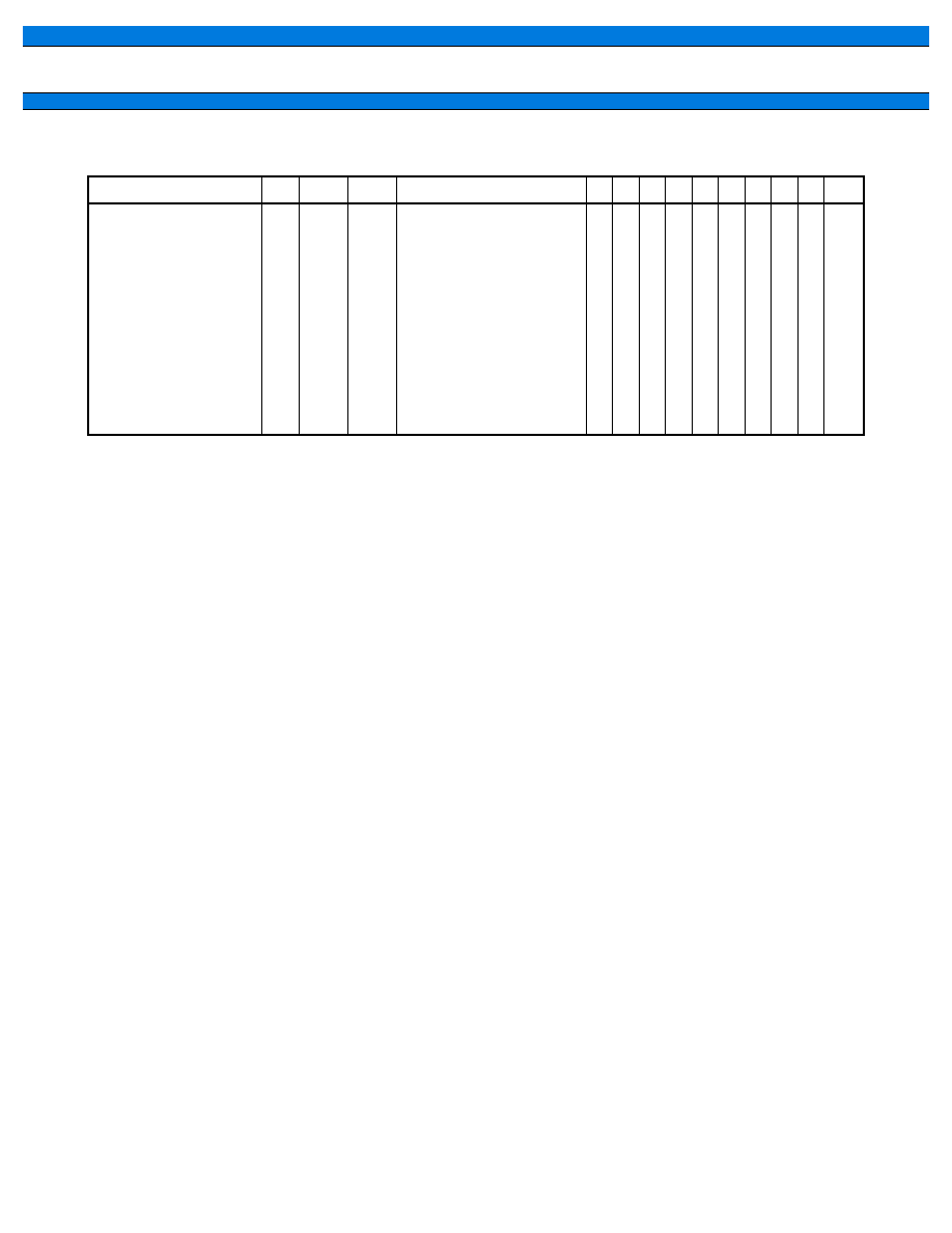
89
MB90220 Series
Table 8 Transfer Instructions (Long Word) [11 Instructions]
For an explanation of "(a)" and "(d)", refer to Table 4, "Number of Execution Cycles for Each Form of Addressing,"
and Table 5, "Correction Values for Number of Cycles Used to Calculate Number of Actual Cycles."
Mnemonic
#
cycles
B
Operation
LH AH
I
S
T
N
Z
V
C
RMW
MOVL A, ear
MOVL A, eam
MOVL A, # imm32
MOVL A, @SP + disp8
MOVPL A, addr24
MOVPL A, @A
MOVPL @A, RLi
MOVL @SP + disp8, A
MOVPL addr24, A
MOVL ear, A
MOVL eam, A
2
2+
5
3
5
2
2
3
5
2
2+
1
3+ (a)
3
4
4
3
5
4
4
2
3+ (a)
0
(d)
0
(d)
(d)
(d)
(d)
(d)
(d)
0
(d)
long (A)
(ear)
long (A)
(eam)
long (A)
imm32
long (A)
((SP) +disp8)
long (A)
(addr24)
long (A)
((A))
long ((A))
(RLi)
long ((SP) + disp8)
(A)
long (addr24)
(A)
long (ear)
(A)
long (eam)
(A)
≠
≠
≠
≠
≠
≠
≠
≠
≠
≠
≠
≠
≠
≠
≠
≠
≠
≠
≠
≠
≠
≠
≠
≠
≠
≠
≠
≠
≠
≠
≠
≠
≠
≠
≠
≠
≠
≠
≠
≠
≠
≠
≠
≠
≠
≠
≠
≠
≠
≠
≠
≠
≠
≠
≠
*
*
*
*
*
*
*
*
*
*
*
*
*
*
*
*
*
*
*
*
*
*
≠
≠
≠
≠
≠
≠
≠
≠
≠
≠
≠
≠
≠
≠
≠
≠
≠
≠
≠
≠
≠
≠
≠
≠
≠
≠
≠
≠
≠
≠
≠
≠
≠
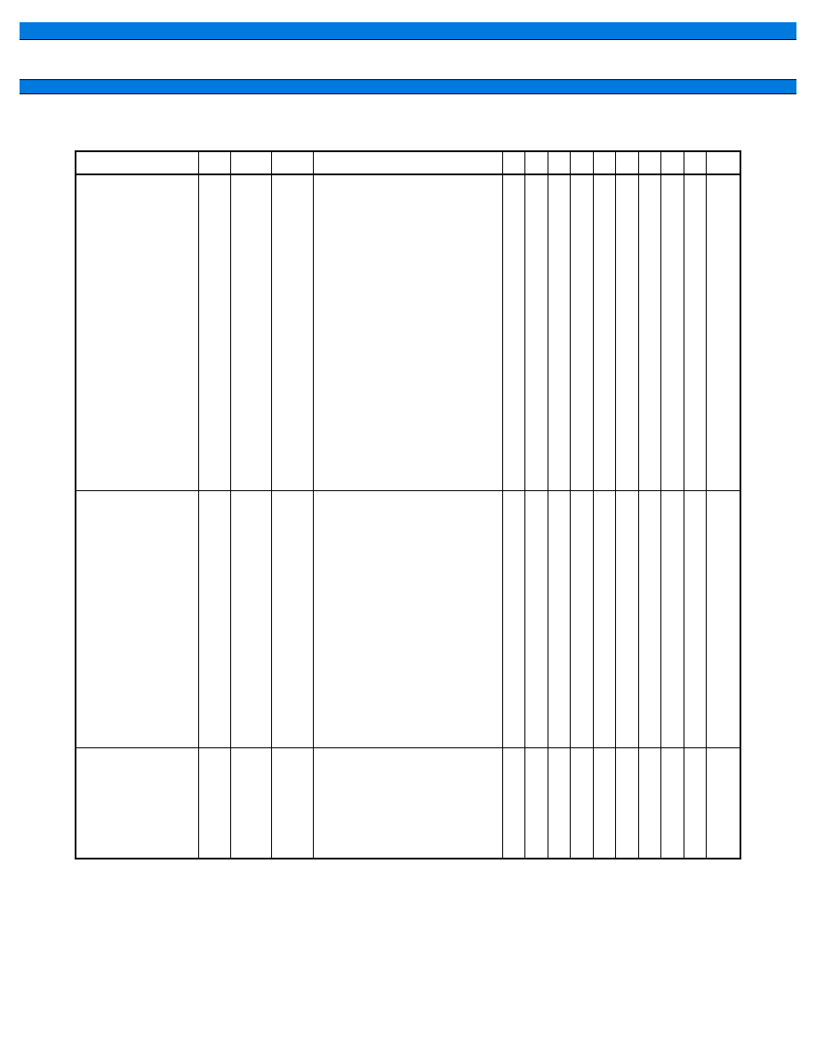
MB90220 Series
90
Table 9 Addition and Subtraction Instructions (Byte/Word/Long Word) [42 Instructions]
For an explanation of "(a)", "(b)", "(c)" and "(d)", refer to Table 4, "Number of Execution Cycles for Each Form of
Addressing," and Table 5, "Correction Values for Number of Cycles Used to Calculate Number of Actual Cycles."
Mnemonic
#
cycles
B
Operation
LH AH
I
S
T
N
Z
V
C
RMW
ADD
A, #imm8
ADD
A, dir
ADD
A, ear
ADD
A, eam
ADD
ear, A
ADD
eam, A
ADDC
A
ADDC
A, ear
ADDC
A, eam
ADDDC A
SUB
A, #imm8
SUB
A, dir
SUB
A, ear
SUB
A, eam
SUB
ear, A
SUB
eam, A
SUBC
A
SUBC
A, ear
SUBC
A, eam
SUBDC A
2
2
2
2+
2
2+
1
2
2+
1
2
2
2
2+
2
2+
1
2
2+
1
2
3
2
3+ (a)
2
3+ (a)
2
2
3+ (a)
3
2
3
2
3+ (a)
2
3+ (a)
2
2
3+ (a)
3
0
(b)
0
(b)
0
2
◊
(b)
0
0
(b)
0
0
(b)
0
(b)
0
2
◊
(b)
0
0
(b)
0
byte (A)
(A) +imm8
byte (A)
(A) +(dir)
byte (A)
(A) +(ear)
byte (A)
(A) +(eam)
byte (ear)
(ear) + (A)
byte (eam)
(eam) + (A)
byte (A)
(AH) + (AL) + (C)
byte (A)
(A) + (ear) + (C)
byte (A)
(A) + (eam) + (C)
byte (A)
(AH) + (AL) + (C) (Decimal)
byte (A)
(A) ≠imm8
byte (A)
(A) ≠ (dir)
byte (A)
(A) ≠ (ear)
byte (A)
(A) ≠ (eam)
byte (ear)
(ear) ≠ (A)
byte (eam)
(eam) ≠ (A)
byte (A)
(AH) ≠ (AL) ≠ (C)
byte (A)
(A) ≠ (ear) ≠ (C)
byte (A)
(A) ≠ (eam) ≠ (C)
byte (A)
(AH) ≠ (AL) ≠ (C) (Decimal)
Z
Z
Z
Z
≠
Z
Z
Z
Z
Z
Z
Z
Z
Z
≠
≠
Z
Z
Z
Z
≠
≠
≠
≠
≠
≠
≠
≠
≠
≠
≠
≠
≠
≠
≠
≠
≠
≠
≠
≠
≠
≠
≠
≠
≠
≠
≠
≠
≠
≠
≠
≠
≠
≠
≠
≠
≠
≠
≠
≠
≠
≠
≠
≠
≠
≠
≠
≠
≠
≠
≠
≠
≠
≠
≠
≠
≠
≠
≠
≠
≠
≠
≠
≠
≠
≠
≠
≠
≠
≠
≠
≠
≠
≠
≠
≠
≠
≠
≠
≠
*
*
*
*
*
*
*
*
*
*
*
*
*
*
*
*
*
*
*
*
*
*
*
*
*
*
*
*
*
*
*
*
*
*
*
*
*
*
*
*
*
*
*
*
*
*
*
*
*
*
*
*
*
*
*
*
*
*
*
*
*
*
*
*
*
*
*
*
*
*
*
*
*
*
*
*
*
*
*
*
≠
≠
≠
≠
*
*
≠
≠
≠
≠
≠
≠
≠
≠
*
*
≠
≠
≠
≠
ADDW A
ADDW A, ear
ADDW A, eam
ADDW A, #imm16
ADDW ear, A
ADDW eam, A
ADDCW A, ear
ADDCW A, eam
SUBW A
SUBW A, ear
SUBW A, eam
SUBW A, #imm16
SUBW ear, A
SUBW eam, A
SUBCW A, ear
SUBCW A, eam
1
2
2+
3
2
2+
2
2+
1
2
2+
3
2
2+
2
2+
2
2
3+ (a)
2
2
3+ (a)
2
3+ (a)
2
2
3+ (a)
2
2
3+ (a)
2
3+ (a)
0
0
(c)
0
0
2
◊
(c)
0
(c)
0
0
(c)
0
0
2
◊
(c)
0
(c)
word (A)
(AH) + (AL)
word (A)
(A) +(ear)
word (A)
(A) +(eam)
word (A)
(A) +imm16
word (ear)
(ear) + (A)
word (eam)
(eam) + (A)
word (A)
(A) + (ear) + (C)
word (A)
(A) + (eam) + (C)
word (A)
(AH) ≠ (AL)
word (A)
(A) ≠ (ear)
word (A)
(A) ≠ (eam)
word (A)
(A) ≠imm16
word (ear)
(ear) ≠ (A)
word (eam)
(eam) ≠ (A)
word (A)
(A) ≠ (ear) ≠ (C)
word (A)
(A) ≠ (eam) ≠ (C)
≠
≠
≠
≠
≠
≠
≠
≠
≠
≠
≠
≠
≠
≠
≠
≠
≠
≠
≠
≠
≠
≠
≠
≠
≠
≠
≠
≠
≠
≠
≠
≠
≠
≠
≠
≠
≠
≠
≠
≠
≠
≠
≠
≠
≠
≠
≠
≠
≠
≠
≠
≠
≠
≠
≠
≠
≠
≠
≠
≠
≠
≠
≠
≠
≠
≠
≠
≠
≠
≠
≠
≠
≠
≠
≠
≠
≠
≠
≠
≠
*
*
*
*
*
*
*
*
*
*
*
*
*
*
*
*
*
*
*
*
*
*
*
*
*
*
*
*
*
*
*
*
*
*
*
*
*
*
*
*
*
*
*
*
*
*
*
*
*
*
*
*
*
*
*
*
*
*
*
*
*
*
*
*
≠
≠
≠
≠
*
*
≠
≠
≠
≠
≠
≠
*
*
≠
≠
ADDL
A, ear
ADDL
A, eam
ADDL
A, #imm32
SUBL
A, ear
SUBL
A, eam
SUBL
A, #imm32
2
2+
5
2
2+
5
5
6+ (a)
4
5
6+ (a)
4
0
(d)
0
0
(d)
0
long (A)
(A) + (ear)
long (A)
(A) + (eam)
long (A)
(A) +imm32
long (A)
(A) ≠ (ear)
long (A)
(A) ≠ (eam)
long (A)
(A) ≠imm32
≠
≠
≠
≠
≠
≠
≠
≠
≠
≠
≠
≠
≠
≠
≠
≠
≠
≠
≠
≠
≠
≠
≠
≠
≠
≠
≠
≠
≠
≠
*
*
*
*
*
*
*
*
*
*
*
*
*
*
*
*
*
*
*
*
*
*
*
*
≠
≠
≠
≠
≠
≠
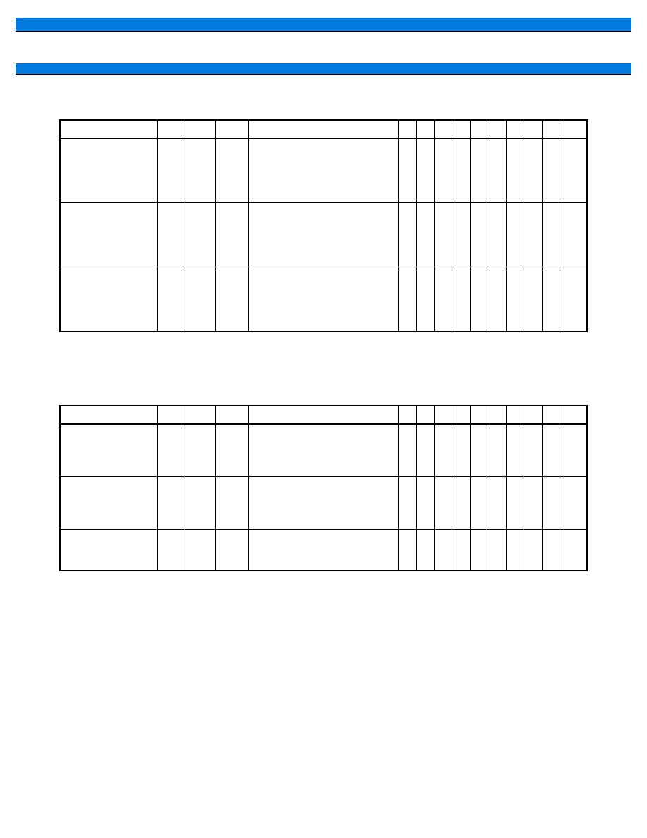
91
MB90220 Series
Table 10 Increment and Decrement Instructions (Byte/Word/Long Word) [12 Instructions]
For an explanation of "(a)", "(b)", "(c)" and "(d)", refer to Table 4, "Number of Execution Cycles for Each Form of
Addressing," and Table 5, "Correction Values for Number of Cycles Used to Calculate Number of Actual Cycles."
Table 11 Compare Instructions (Byte/Word/Long Word) [11 Instructions]
For an explanation of "(a)", "(b)", "(c)" and "(d)", refer to Table 4, "Number of Execution Cycles for Each Form of
Addressing," and Table 5, "Correction Values for Number of Cycles Used to Calculate Number of Actual Cycles."
Mnemonic
#
cycles
B
Operation
LH AH
I
S
T
N
Z
V
C
RMW
INC
ear
INC
eam
DEC
ear
DEC
eam
2
2+
2
2+
2
3+ (a)
2
3+ (a)
0
2
◊
(b)
0
2
◊
(b)
byte (ear)
(ear) +1
byte (eam)
(eam) +1
byte (ear)
(ear) ≠1
byte (eam)
(eam) ≠1
≠
≠
≠
≠
≠
≠
≠
≠
≠
≠
≠
≠
≠
≠
≠
≠
≠
≠
≠
≠
*
*
*
*
*
*
*
*
*
*
*
*
≠
≠
≠
≠
*
*
*
*
INCW
ear
INCW
eam
DECW ear
DECW eam
2
2+
2
2+
2
3+ (a)
2
3+ (a)
0
2
◊
(c)
0
2
◊
(c)
word (ear)
(ear) +1
word (eam)
(eam) +1
word (ear)
(ear) ≠1
word (eam)
(eam) ≠1
≠
≠
≠
≠
≠
≠
≠
≠
≠
≠
≠
≠
≠
≠
≠
≠
≠
≠
≠
≠
*
*
*
*
*
*
*
*
*
*
*
*
≠
≠
≠
≠
*
*
*
*
INCL
ear
INCL
eam
DECL
ear
DECL
eam
2
2+
2
2+
4
5+ (a)
4
5+ (a)
0
2
◊
(d)
0
2
◊
(d)
long (ear)
(ear) +1
long (eam)
(eam) +1
long (ear)
(ear) ≠1
long (eam)
(eam) ≠1
≠
≠
≠
≠
≠
≠
≠
≠
≠
≠
≠
≠
≠
≠
≠
≠
≠
≠
≠
≠
*
*
*
*
*
*
*
*
*
*
*
*
≠
≠
≠
≠
*
*
*
*
Mnemonic
#
cycles
B
Operation
LH AH
I
S
T
N
Z
V
C
RMW
CMP
A
CMP
A, ear
CMP
A, eam
CMP
A, #imm8
1
2
2+
2
2
2
2+ (a)
2
0
0
(b)
0
byte (AH) ≠ (AL)
byte (A) ≠ (ear)
byte (A) ≠ (eam)
byte (A) ≠ imm8
≠
≠
≠
≠
≠
≠
≠
≠
≠
≠
≠
≠
≠
≠
≠
≠
≠
≠
≠
≠
*
*
*
*
*
*
*
*
*
*
*
*
*
*
*
*
≠
≠
≠
≠
CMPW A
CMPW A, ear
CMPW A, eam
CMPW A, #imm16
1
2
2+
3
2
2
2+ (a)
2
0
0
(c)
0
word (AH) ≠ (AL)
word (A) ≠ (ear)
word (A) ≠ (eam)
word (A) ≠ imm16
≠
≠
≠
≠
≠
≠
≠
≠
≠
≠
≠
≠
≠
≠
≠
≠
≠
≠
≠
≠
*
*
*
*
*
*
*
*
*
*
*
*
*
*
*
*
≠
≠
≠
≠
CMPL A, ear
CMPL A, eam
CMPL A, #imm32
2
2+
5
3
4+ (a)
3
0
(d)
0
long (A) ≠ (ear)
long (A) ≠ (eam)
long (A) ≠ imm32
≠
≠
≠
≠
≠
≠
≠
≠
≠
≠
≠
≠
≠
≠
≠
*
*
*
*
*
*
*
*
*
*
*
*
≠
≠
≠
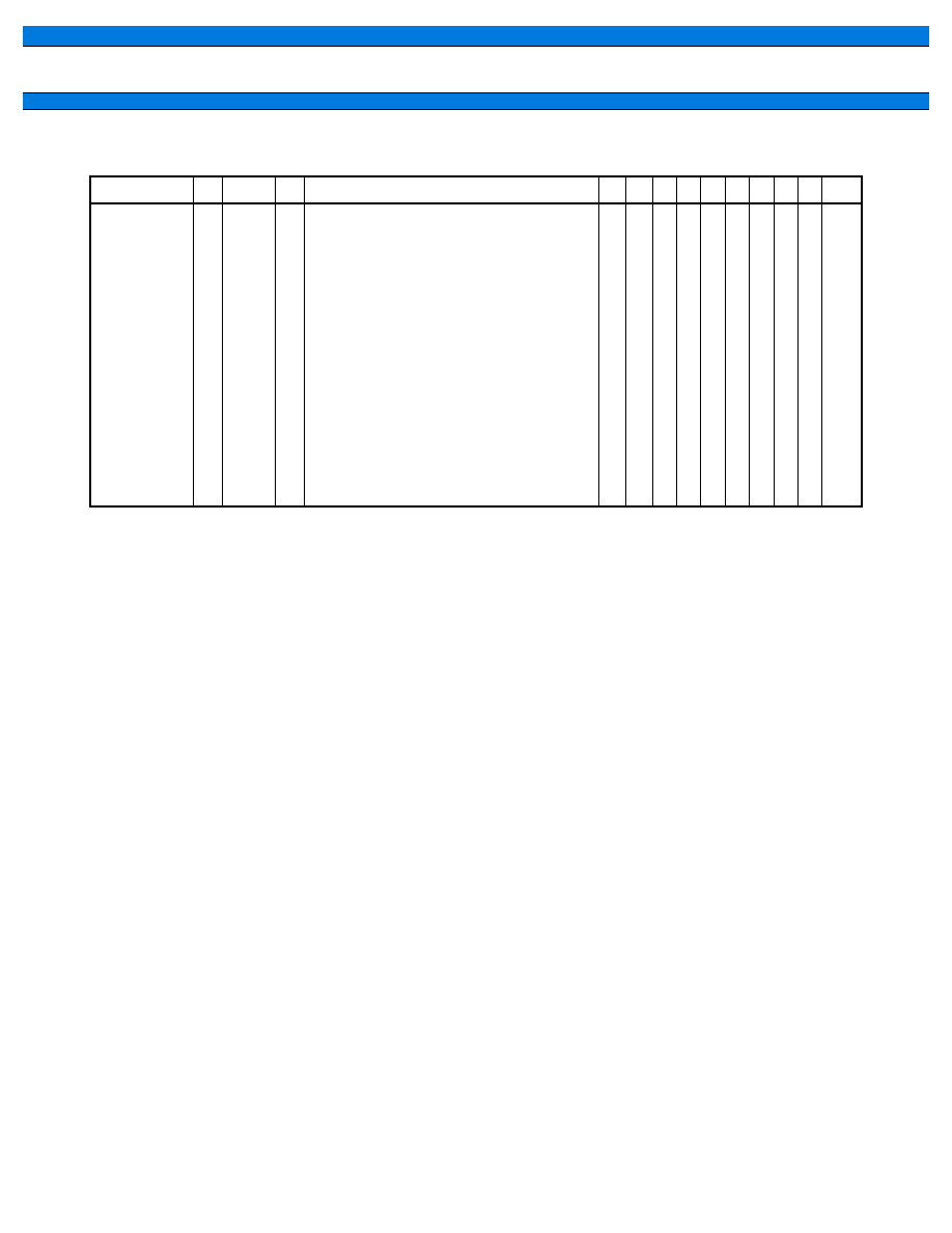
MB90220 Series
92
Table 12 Unsigned Multiplication and Division Instructions (Word/Long Word) [11 Instructions]
For an explanation of "(b)" and "(c), refer to Table 5, "Correction Values for Number of Cycle Used to Calculate
Number of Actual Cycles."
*1: 3 when dividing into zero, 6 when an overflow occurs, and 14 normally.
*2: 3 when dividing into zero, 5 when an overflow occurs, and 13 normally.
*3: 5 + (a) when dividing into zero, 7 + (a) when an overflow occurs, and 17 + (a) normally.
*4: 3 when dividing into zero, 5 when an overflow occurs, and 21 normally.
*5: 4 + (a) when dividing into zero, 7 + (a) when an overflow occurs, and 25 + (a) normally.
*6: (b) when dividing into zero or when an overflow occurs, and 2
◊
(b) normally.
*7: (c) when dividing into zero or when an overflow occurs, and 2
◊
(c) normally.
*8: 3 when byte (AH) is zero, and 7 when byte (AH) is not 0.
*9: 3 when byte (ear) is zero, and 7 when byte (ear) is not 0.
*10: 4 + (a) when byte (eam) is zero, and 8 + (a) when byte (eam) is not 0.
*11: 3 when word (AH) is zero, and 11 when word (AH) is not 0.
*12: 3 when word (ear) is zero, and 11 when word (ear) is not 0.
*13: 4 + (a) when word (eam) is zero, and 12 + (a) when word (eam) is not 0.
Mnemonic
#
cycles
B
Operation
LH AH
I
S T N Z V C
RMW
DIVU A
DIVU A, ear
DIVU A, eam
DIVUW A, ear
DIVUW A, eam
MULU A
MULU A, ear
MULU A, eam
MULUW A
MULUW A, ear
MULUW A, eam
1
2
2+
2
2+
1
2
2+
1
2
2+
*
1
*
2
*
3
*
4
*
5
*
8
*
9
*
10
*
11
*
12
*
13
0
0
*
6
0
*
7
0
0
(b)
0
0
(c)
word (AH) /byte (AL)
Quotient
byte (AL) Remainder
byte (AH)
word (A)/byte (ear)
Quotient
byte (A) Remainder
byte (ear)
word (A)/byte (eam)
Quotient
byte (A) Remainder
byte (eam)
long (A)/word (ear)
Quotient
word (A) Remainder
word (ear)
long (A)/word (eam)
Quotient
word (A) Remainder
word (eam)
byte (AH)
◊
byte (AL)
word (A)
byte (A)
◊
byte (ear)
word (A)
byte (A)
◊
byte (eam)
word (A)
word (AH)
◊
word (AL)
long (A)
word (A)
◊
word (ear)
long (A)
word (A)
◊
word (eam)
long (A)
≠
≠
≠
≠
≠
≠
≠
≠
≠
≠
≠
≠
≠
≠
≠
≠
≠
≠
≠
≠
≠
≠
≠
≠
≠
≠
≠
≠
≠
≠
≠
≠
≠
≠
≠
≠
≠
≠
≠
≠
≠
≠
≠
≠
≠
≠
≠
≠
≠
≠
≠
≠
≠
≠
≠
≠
≠
≠
≠
≠
≠
≠
≠
≠
≠
≠
≠
≠
≠
≠
≠
≠
≠
≠
≠
≠
≠
*
*
*
*
*
≠
≠
≠
≠
≠
≠
*
*
*
*
*
≠
≠
≠
≠
≠
≠
≠
≠
≠
≠
≠
≠
≠
≠
≠
≠
≠
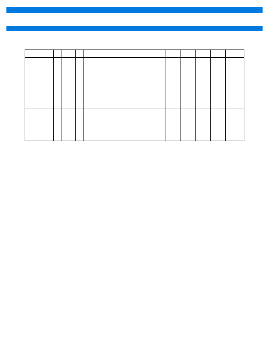
93
MB90220 Series
Table 13 Signed Multiplication and Division Instructions (Word/Long Word) [11 Insturctions]
For an explanation of "(b)" and "(c)", refer to Table 5, "Correction Values for Number of Cycles Used to Calculate
Number of Actual Cycles."
*1: 3 when dividing into zero, 8 or 18 when an overflow occurs, and 18 normally.
*2: 3 when dividing into zero, 10 or 21 when an overflow occurs, and 22 normally.
*3: 4 + (a) when dividing into zero, 11 + (a) or 22 + (a) when an overflow occurs, and 23 + (a) normally.
*4: When the dividend is positive: 4 when dividing into zero, 10 or 29 when an overflow occurs, and 30 normally.
When the dividend is negative: 4 when dividing into zero, 11 or 30 when an overflow occurs, and 31 normally.
*5: When the dividend is positive: 4 + (a) when dividing into zero, 11 + (a) or 30 + (a) when an overflow occurs,
and 31 + (a) normally.
When the dividend is negative: 4 + (a) when dividing into zero, 12 + (a) or 31 + (a) when an overflow occurs,
and 32 + (a) normally.
*6: (b) when dividing into zero or when an overflow occurs, and 2
◊
(b) normally.
*7: (c) when dividing into zero or when an overflow occurs, and 2
◊
(c) normally.
*8: 3 when byte (AH) is zero, 12 when the result is positive, and 13 when the result is negative.
*9: 3 when byte (ear) is zero, 12 when the result is positive, and 13 when the result is negative.
*10: 4 + (a) when byte (eam) is zero, 13 + (a) when the result is positive, and 14 + (a) when the result is negative.
*11: 3 when word (AH) is zero, 12 when the result is positive, and 13 when the result is negative.
*12: 3 when word (ear) is zero, 16 when the result is positive, and 19 when the result is negative.
*13: 4 + (a) when word (eam) is zero, 17 + (a) when the result is positive, and 20 + (a) when the result is negative.
Note: Which of the two values given for the number of execution cycles applies when an overflow error occurs in
a DIV or DIVW instruction depends on whether the overflow was detected before or after the operation.
Mnemonic
#
cycles
B
Operation
LH AH
I
S
T
N
Z
V
C
RMW
DIV
A
DIV
A, ear
DIV
A, eam
DIVW A, ear
DIVW A, eam
2
2
2+
2
2+
*
1
*
2
*
3
*
4
*
5
0
0
*
6
0
*
7
word (AH) /byte (AL)
Quotient
byte (AL) Remainder
byte (AH)
word (A)/byte (ear)
Quotient
byte (A) Remainder
byte (ear)
word (A)/byte (eam)
Quotient
byte (A) Remainder
byte (eam)
long (A)/word (ear)
Quotient
word (A) Remainder
word (ear)
long (A)/word (eam)
Quotient
word (A) Remainder
word (eam)
Z
Z
Z
≠
≠
≠
≠
≠
≠
≠
≠
≠
≠
≠
≠
≠
≠
≠
≠
≠
≠
≠
≠
≠
≠
≠
≠
≠
≠
≠
≠
≠
≠
≠
≠
*
*
*
*
*
*
*
*
*
*
≠
≠
≠
≠
≠
MUL A
MUL A, ear
MUL A, eam
MULW A
MULW A, ear
MULW A, eam
2
2
2+
2
2
2+
*
8
*
9
*
10
*
11
*
12
*
13
0
0
(b)
0
0
(b)
byte (AH)
◊
byte (AL)
word (A)
byte (A)
◊
byte (ear)
word (A)
byte (A)
◊
byte (eam)
word (A)
word (AH)
◊
word (AL)
long (A)
word (A)
◊
word (ear)
long (A)
word (A)
◊
word (eam)
long (A)
≠
≠
≠
≠
≠
≠
≠
≠
≠
≠
≠
≠
≠
≠
≠
≠
≠
≠
≠
≠
≠
≠
≠
≠
≠
≠
≠
≠
≠
≠
≠
≠
≠
≠
≠
≠
≠
≠
≠
≠
≠
≠
≠
≠
≠
≠
≠
≠
≠
≠
≠
≠
≠
≠
≠
≠
≠
≠
≠
≠
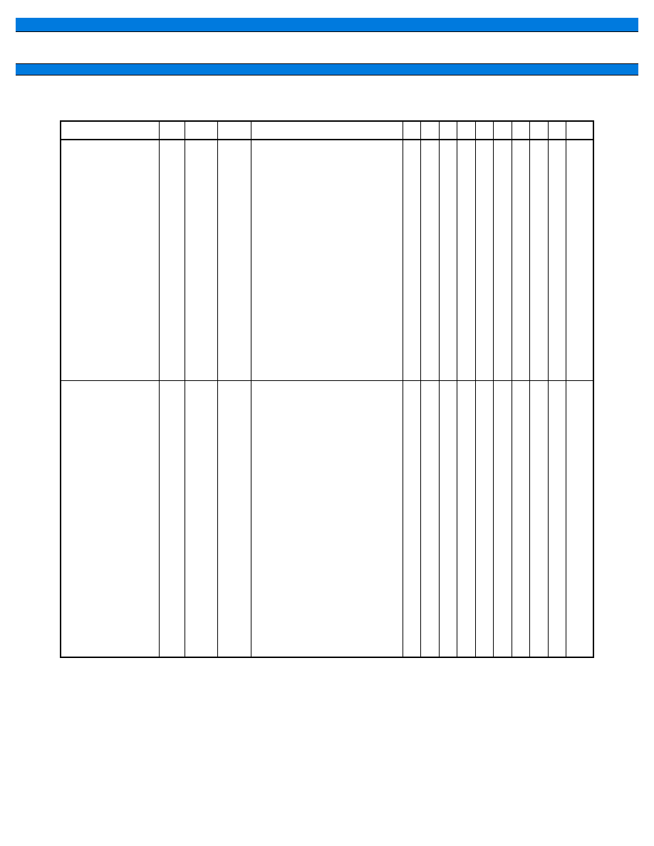
MB90220 Series
94
Table 14 Logical 1 Instructions (Byte, Word) [39 Instructions]
For an explanation of "(a)", "(b)", "(c)" and "(d)", refer to Table 4, "Number of Execution Cycles for Each Form of
Addressing," and Table 5, "Correction Values for Number of Cycles Used to Calculate Number of Actual Cycles."
Mnemonic
#
cycles
B
Operation
LH AH
I
S
T
N
Z
V
C
RMW
AND
A, #imm8
AND
A, ear
AND
A, eam
AND
ear, A
AND
eam, A
OR
A, #imm8
OR
A, ear
OR
A, eam
OR
ear, A
OR
eam, A
XOR
A, #imm8
XOR
A, ear
XOR
A, eam
XOR
ear, A
XOR
eam, A
NOT
A
NOT
ear
NOT
eam
2
2
2+
2
2+
2
2
2+
2
2+
2
2
2+
2
2+
1
2
2+
2
2
3+ (a)
3
3+ (a)
2
2
3+ (a)
3
3+ (a)
2
2
3+ (a)
3
3+ (a)
2
2
3+ (a)
0
0
(b)
0
2
◊
(b)
0
0
(b)
0
2
◊
(b)
0
0
(b)
0
2
◊
(b)
0
0
2
◊
(b)
byte (A)
(A) and imm8
byte (A)
(A) and (ear)
byte (A)
(A) and (eam)
byte (ear)
(ear) and (A)
byte (eam)
(eam) and (A)
byte (A)
(A) or imm8
byte (A)
(A) or (ear)
byte (A)
(A) or (eam)
byte (ear)
(ear) or (A)
byte (eam)
(eam) or (A)
byte (A)
(A) xor imm8
byte (A)
(A) xor (ear)
byte (A)
(A) xor (eam)
byte (ear)
(ear) xor (A)
byte (eam)
(eam) xor (A)
byte (A)
not (A)
byte (ear)
not (ear)
byte (eam)
not (eam)
≠
≠
≠
≠
≠
≠
≠
≠
≠
≠
≠
≠
≠
≠
≠
≠
≠
≠
≠
≠
≠
≠
≠
≠
≠
≠
≠
≠
≠
≠
≠
≠
≠
≠
≠
≠
≠
≠
≠
≠
≠
≠
≠
≠
≠
≠
≠
≠
≠
≠
≠
≠
≠
≠
≠
≠
≠
≠
≠
≠
≠
≠
≠
≠
≠
≠
≠
≠
≠
≠
≠
≠
≠
≠
≠
≠
≠
≠
≠
≠
≠
≠
≠
≠
≠
≠
≠
≠
≠
≠
*
*
*
*
*
*
*
*
*
*
*
*
*
*
*
*
*
*
*
*
*
*
*
*
*
*
*
*
*
*
*
*
*
*
*
*
R
R
R
R
R
R
R
R
R
R
R
R
R
R
R
R
R
R
≠
≠
≠
≠
≠
≠
≠
≠
≠
≠
≠
≠
≠
≠
≠
≠
≠
≠
≠
≠
≠
*
*
≠
≠
≠
*
*
≠
≠
≠
*
*
≠
*
*
ANDW A
ANDW A, #imm16
ANDW A, ear
ANDW A, eam
ANDW ear, A
ANDW eam, A
ORW
A
ORW
A, #imm16
ORW
A, ear
ORW
A, eam
ORW
ear, A
ORW
eam, A
XORW A
XORW A, #imm16
XORW A, ear
XORW A, eam
XORW ear, A
XORW eam, A
NOTW A
NOTW ear
NOTW eam
1
3
2
2+
2
2+
1
3
2
2+
2
2+
1
3
2
2+
2
2+
1
2
2+
2
2
2
3+ (a)
3
3+ (a)
2
2
2
3+ (a)
3
3+ (a)
2
2
2
3+ (a)
3
3+ (a)
2
2
3+ (a)
0
0
0
(c)
0
2
◊
(c)
0
0
0
(c)
0
2
◊
(c)
0
0
0
(c)
0
2
◊
(c)
0
0
2
◊
(c)
word (A)
(AH) and (A)
word (A)
(A) and imm16
word (A)
(A) and (ear)
word (A)
(A) and (eam)
word (ear)
(ear) and (A)
word (eam)
(eam) and (A)
word (A)
(AH) or (A)
word (A)
(A) or imm16
word (A)
(A) or (ear)
word (A)
(A) or (eam)
word (ear)
(ear) or (A)
word (eam)
(eam) or (A)
word (A)
(AH) xor (A)
word (A)
(A) xor imm16
word (A)
(A) xor (ear)
word (A)
(A) xor (eam)
word (ear)
(ear) xor (A)
word (eam)
(eam) xor (A)
word (A)
not (A)
word (ear)
not (ear)
word (eam)
not (eam)
≠
≠
≠
≠
≠
≠
≠
≠
≠
≠
≠
≠
≠
≠
≠
≠
≠
≠
≠
≠
≠
≠
≠
≠
≠
≠
≠
≠
≠
≠
≠
≠
≠
≠
≠
≠
≠
≠
≠
≠
≠
≠
≠
≠
≠
≠
≠
≠
≠
≠
≠
≠
≠
≠
≠
≠
≠
≠
≠
≠
≠
≠
≠
≠
≠
≠
≠
≠
≠
≠
≠
≠
≠
≠
≠
≠
≠
≠
≠
≠
≠
≠
≠
≠
≠
≠
≠
≠
≠
≠
≠
≠
≠
≠
≠
≠
≠
≠
≠
≠
≠
≠
≠
≠
≠
*
*
*
*
*
*
*
*
*
*
*
*
*
*
*
*
*
*
*
*
*
*
*
*
*
*
*
*
*
*
*
*
*
*
*
*
*
*
*
*
*
*
R
R
R
R
R
R
R
R
R
R
R
R
R
R
R
R
R
R
R
R
R
≠
≠
≠
≠
≠
≠
≠
≠
≠
≠
≠
≠
≠
≠
≠
≠
≠
≠
≠
≠
≠
≠
≠
≠
≠
*
*
≠
≠
≠
≠
*
*
≠
≠
≠
≠
*
*
≠
*
*
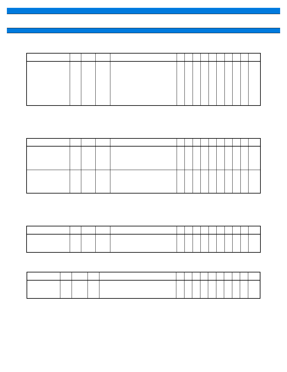
95
MB90220 Series
Table 15 Logical 2 Instructions (Long Word) [6 Instructions]
For an explanation of "(a)" and "(d)", refer to Table 4, "Number of Execution Cycles for Each Form of Addressing,"
and Table 5, "Correction Values for Number of Cycles Used to Calculate Number of Actual Cycles."
Table 16 Sign Inversion Instructions (Byte/Word) [6 Instructions]
For an explanation of "(a)", "(b)" and "(c)" and refer to Table 4, "Number of Execution Cycles for Each Form of
Addressing," and Table 5, "Correction Values for Number of Cycles Used to Calculate Number of Actual Cycles."
Table 17 Absolute Value Instructions (Byte/Word/Long Word) [3 Insturctions]
Table 18 Normalize Instructions (Long Word) [1 Instruction]
* : 5 when the contents of the accumulator are all zeroes, 5 + (R0) in all other cases.
Mnemonic
#
cycles
B
Operation
LH AH
I
S
T
N
Z
V
C
RMW
ANDL
A, ear
ANDL
A, eam
ORL
A, ear
ORL
A, eam
XORL A, ear
XORL A, eam
2
2+
2
2+
2
2+
5
6+ (a)
5
6+ (a)
5
6+ (a)
0
(d)
0
(d)
0
(d)
long (A)
(A) and (ear)
long (A)
(A) and (eam)
long (A)
(A) or (ear)
long (A)
(A) or (eam)
long (A)
(A) xor (ear)
long (A)
(A) xor (eam)
≠
≠
≠
≠
≠
≠
≠
≠
≠
≠
≠
≠
≠
≠
≠
≠
≠
≠
≠
≠
≠
≠
≠
≠
≠
≠
≠
≠
≠
≠
*
*
*
*
*
*
*
*
*
*
*
*
R
R
R
R
R
R
≠
≠
≠
≠
≠
≠
≠
≠
≠
≠
≠
≠
Mnemonic
#
cycles
B
Operation
LH AH
I
S
T
N
Z
V
C
RMW
NEG
A
NEG
ear
NEG
eam
1
2
2+
2
2
3+ (a)
0
0
2
◊
(b)
byte (A)
0 ≠ (A)
byte (ear)
0 ≠ (ear)
byte (eam)
0 ≠ (eam)
X
≠
≠
≠
≠
≠
≠
≠
≠
≠
≠
≠
≠
≠
≠
*
*
*
*
*
*
*
*
*
*
*
*
≠
*
*
NEGW A
NEGW ear
NEGW eam
1
2
2+
2
2
3+ (a)
0
0
2
◊
(c)
word (A)
0 ≠ (A)
word (ear)
0 ≠ (ear)
word (eam)
0 ≠ (eam)
≠
≠
≠
≠
≠
≠
≠
≠
≠
≠
≠
≠
≠
≠
≠
*
*
*
*
*
*
*
*
*
*
*
*
≠
*
*
Mnemonic
#
cycles
B
Operation
LH AH
I
S
T
N
Z
V
C
RMW
ABS
A
ABSW A
ABSL
A
2
2
2
2
2
4
0
0
0
byte (A)
absolute value (A)
word (A)
absolute value (A)
long (A)
absolute value (A)
Z
≠
≠
≠
≠
≠
≠
≠
≠
≠
≠
≠
≠
≠
≠
*
*
*
*
*
*
*
*
*
≠
≠
≠
≠
≠
≠
Mnemonic
#
cycles
B
Operation
LH AH
I
S
T
N
Z
V
C
RMW
NRML A, R0
2
*
0
long (A)
Shifts to the position at
which "1" was set first
byte (R0)
current shift count
≠
≠
≠
≠
*
≠
≠
≠
≠
≠
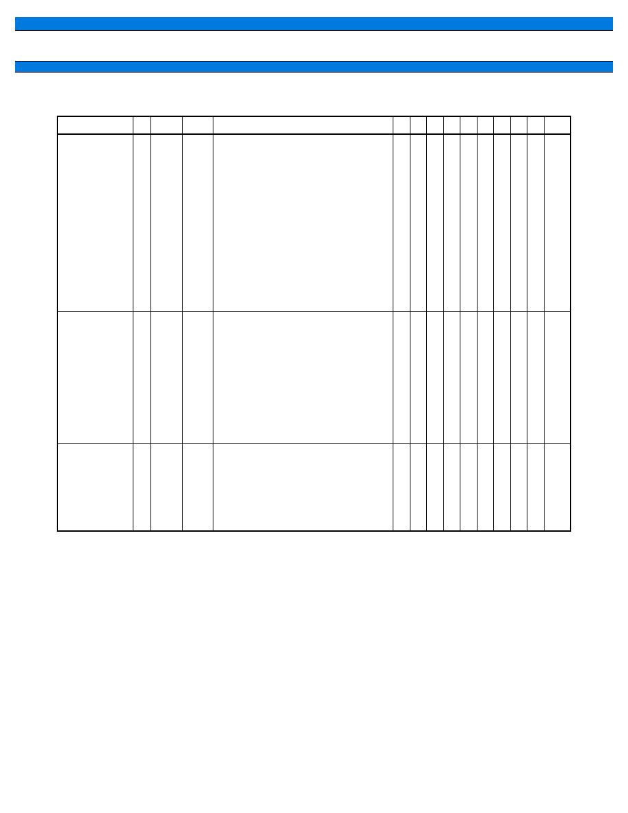
MB90220 Series
96
Table 19 Shift Instructions (Byte/Word/Long Word) [27 Instructions]
For an explanation of "(a)" and "(b)", refer to Table 4, "Number of Execution Cycles for Each Form of Addressing,"
and Table 5, "Correction Values for Number of Cycles Used to Calculate Number of Actual Cycles."
*1: 3 when R0 is 0, 3 + (R0) in all other cases.
*2: 3 when R0 is 0, 4 + (R0) in all other cases.
*3: 3 when imm8 is 0, 3 + (imm8) in all other cases.
*4: 3 when imm8 is 0, 4 + (imm8) in all other cases.
Mnemonic
#
cycles
B
Operation
LH AH
I
S
T
N
Z
V
C
RMW
RORC A
ROLC A
RORC ear
RORC eam
ROLC ear
ROLC eam
ASR
A, R0
LSR
A, R0
LSL
A, R0
ASR A, #imm8
LSR A, #imm8
LSL A, #imm8
2
2
2
2+
2
2+
2
2
2
3
3
3
2
2
2
3+ (a)
2
3+ (a)
*
1
*
1
*
1
*
3
*
3
*
3
0
0
0
2
◊
(b)
0
2
◊
(b)
0
0
0
0
0
0
byte (A)
Right rotation with carry
byte (A)
Left rotation with carry
byte (ear)
Right rotation with carry
byte (eam)
Right rotation with carry
byte (ear)
Left rotation with carry
byte (eam)
Left rotation with carry
byte (A)
Arithmetic right barrel shift (A, R0)
byte (A)
Logical right barrel shift (A, R0)
byte (A)
Logical left barrel shift (A, R0)
byte (A)
Arithmetic right barrel shift (A, imm8)
byte (A)
Logical right barrel shift (A, imm8)
byte (A)
Logical left barrel shift (A, imm8)
≠
≠
≠
≠
≠
≠
≠
≠
≠
≠
≠
≠
≠
≠
≠
≠
≠
≠
≠
≠
≠
≠
≠
≠
≠
≠
≠
≠
≠
≠
≠
≠
≠
≠
≠
≠
≠
≠
≠
≠
≠
≠
≠
≠
≠
≠
≠
≠
≠
≠
≠
≠
≠
≠
*
*
≠
*
*
≠
*
*
*
*
*
*
*
*
*
*
*
*
*
*
*
*
*
*
*
*
*
*
*
*
≠
≠
≠
≠
≠
≠
≠
≠
≠
≠
≠
≠
*
*
*
*
*
*
*
*
*
*
*
*
≠
≠
*
*
*
*
≠
≠
≠
≠
≠
≠
ASRW A
LSRW A/SHRW A
LSLW A/SHLW A
ASRW A, R0
LSRW A, R0
LSLW A, R0
ASRW A, #imm8
LSRW A, #imm8
LSLW A, #imm8
1
1
1
2
2
2
3
3
3
2
2
2
*
1
*
1
*
1
*
3
*
3
*
3
0
0
0
0
0
0
0
0
0
word (A)
Arithmetic right shift (A, 1 bit)
word (A)
Logical right shift (A, 1 bit)
word (A)
Logical left shift (A, 1 bit)
word (A)
Arithmetic right barrel shift (A, R0)
word (A)
Logical right barrel shift (A, R0)
word (A)
Logical left barrel shift (A, R0)
word (A)
Arithmetic right barrel shift (A, imm8)
word (A)
Logical right barrel shift (A, imm8)
word (A)
Logical left barrel shift (A, imm8)
≠
≠
≠
≠
≠
≠
≠
≠
≠
≠
≠
≠
≠
≠
≠
≠
≠
≠
≠
≠
≠
≠
≠
≠
≠
≠
≠
≠
≠
≠
≠
≠
≠
≠
≠
≠
*
*
≠
*
*
≠
*
*
≠
*
R
*
*
*
*
*
*
*
*
*
*
*
*
*
*
*
*
≠
≠
≠
≠
≠
≠
≠
≠
≠
*
*
*
*
*
*
*
*
*
≠
≠
≠
≠
≠
≠
≠
≠
≠
ASRL A, R0
LSRL A, R0
LSLL
A, R0
ASRL A, #imm8
LSRL A, #imm8
LSLL
A, #imm8
2
2
2
3
3
3
*
2
*
2
*
2
*
4
*
4
*
4
0
0
0
0
0
0
long (A)
Arithmetic right shift (A, R0)
long (A)
Logical right barrel shift (A, R0)
long (A)
Logical left barrel shift (A, R0)
long (A)
Arithmetic right shift (A, imm8)
long (A)
Logical right barrel shift (A, imm8)
long (A)
Logical left barrel shift (A, imm8)
≠
≠
≠
≠
≠
≠
≠
≠
≠
≠
≠
≠
≠
≠
≠
≠
≠
≠
≠
≠
≠
≠
≠
≠
*
*
≠
*
*
≠
*
*
*
*
*
*
*
*
*
*
*
*
≠
≠
≠
≠
≠
≠
*
*
*
*
*
*
≠
≠
≠
≠
≠
≠
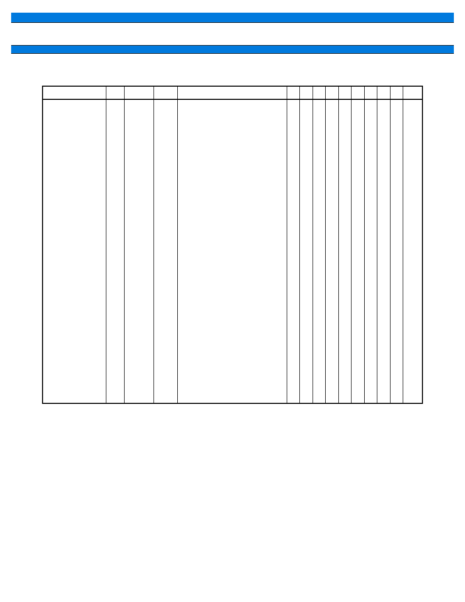
97
MB90220 Series
Table 20 Branch 1 Instructions [31 Instructions]
For an explanation of "(a)", "(c)" and "(d)", refer to Table 4, "Number of Execution Cycles for Each Form of Addressing,"
and Table 5, "Correction Values for Number of Cycles Used to Calculate Number of Actual Cycles."
*1: 3 when branching, 2 when not branching.
*2: 3
◊
(c) + (b)
*3: Read (word) branch address.
*4: W: Save (word) to stack; R: Read (word) branch address.
*5: Save (word) to stack.
*6: W: Save (long word) to W stack; R: Read (long word) branch address.
*7: Save (long word) to stack.
Mnemonic
#
cycles
B
Operation
LH AH
I
S
T
N
Z
V
C
RMW
BZ/BEQ
rel
BNZ/BNE
rel
BC/BLO
rel
BNC/BHS
rel
BN
rel
BP
rel
BV
rel
BNV
rel
BT
rel
BNT
rel
BLT
rel
BGE
rel
BLE
rel
BGT
rel
BLS
rel
BHI
rel
BRA
rel
JMP
@A
JMP
addr16
JMP
@ear
JMP
@eam
JMPP
@ear *
3
JMPP
@eam *
3
JMPP
addr24
CALL
@ear *
4
CALL
@eam *
4
CALL
addr16 *
5
CALLV #vct4 *
5
CALLP @ear *
6
CALLP @eam *
6
CALLP addr24 *
7
2
2
2
2
2
2
2
2
2
2
2
2
2
2
2
2
2
1
3
2
2+
2
2+
4
2
2+
3
1
2
2+
4
*
1
*
1
*
1
*
1
*
1
*
1
*
1
*
1
*
1
*
1
*
1
*
1
*
1
*
1
*
1
*
1
*
1
2
2
3
4+ (a)
3
4+ (a)
3
4
5+ (a)
5
5
7
8+ (a)
7
0
0
0
0
0
0
0
0
0
0
0
0
0
0
0
0
0
0
0
0
(c)
0
(d)
0
(c)
2
◊
(c)
(c)
2
◊
(c)
2
◊
(c)
*
2
2
◊
(c)
Branch when (Z) = 1
Branch when (Z) = 0
Branch when (C) = 1
Branch when (C) = 0
Branch when (N) = 1
Branch when (N) = 0
Branch when (V) = 1
Branch when (V) = 0
Branch when (T) = 1
Branch when (T) = 0
Branch when (V) xor (N) = 1
Branch when (V) xor (N) = 0
( (V) xor (N) ) or (Z) = 1
( (V) xor (N) ) or (Z) = 0
Branch when (C) or (Z) = 1
Branch when (C) or (Z) = 0
Branch unconditionally
word (PC)
(A)
word (PC)
addr16
word (PC)
(ear)
word (PC)
(eam)
word (PC)
(ear), (PCB)
(ear +2)
word (PC)
(eam), (PCB)
(eam +2)
word (PC)
ad24 0 to 15
(PCB)
ad24 16 to 23
word (PC)
(ear)
word (PC)
(eam)
word (PC)
addr16
Vector call linstruction
word (PC)
(ear) 0 to 15,
(PCB)
(ear) 16 to 23
word (PC)
(eam) 0 to 15,
(PCB)
(eam) 16 to 23
word (PC)
addr 0 to 15,
(PCB)
addr 16 to 23
≠
≠
≠
≠
≠
≠
≠
≠
≠
≠
≠
≠
≠
≠
≠
≠
≠
≠
≠
≠
≠
≠
≠
≠
≠
≠
≠
≠
≠
≠
≠
≠
≠
≠
≠
≠
≠
≠
≠
≠
≠
≠
≠
≠
≠
≠
≠
≠
≠
≠
≠
≠
≠
≠
≠
≠
≠
≠
≠
≠
≠
≠
≠
≠
≠
≠
≠
≠
≠
≠
≠
≠
≠
≠
≠
≠
≠
≠
≠
≠
≠
≠
≠
≠
≠
≠
≠
≠
≠
≠
≠
≠
≠
≠
≠
≠
≠
≠
≠
≠
≠
≠
≠
≠
≠
≠
≠
≠
≠
≠
≠
≠
≠
≠
≠
≠
≠
≠
≠
≠
≠
≠
≠
≠
≠
≠
≠
≠
≠
≠
≠
≠
≠
≠
≠
≠
≠
≠
≠
≠
≠
≠
≠
≠
≠
≠
≠
≠
≠
≠
≠
≠
≠
≠
≠
≠
≠
≠
≠
≠
≠
≠
≠
≠
≠
≠
≠
≠
≠
≠
≠
≠
≠
≠
≠
≠
≠
≠
≠
≠
≠
≠
≠
≠
≠
≠
≠
≠
≠
≠
≠
≠
≠
≠
≠
≠
≠
≠
≠
≠
≠
≠
≠
≠
≠
≠
≠
≠
≠
≠
≠
≠
≠
≠
≠
≠
≠
≠
≠
≠
≠
≠
≠
≠
≠
≠
≠
≠
≠
≠
≠
≠
≠
≠
≠
≠
≠
≠
≠
≠
≠
≠
≠
≠
≠
≠
≠
≠
≠
≠
≠
≠
≠
≠
≠
≠
≠
≠
≠
≠
≠
≠
≠
≠
≠
≠
≠
≠
≠
≠
≠
≠
≠
≠
≠
≠
≠
≠
≠
≠
≠
≠
≠
≠
≠
≠
≠
≠
≠
≠
≠
≠
≠
≠
≠
≠
≠
≠
≠
≠
≠
≠
≠
≠
≠
≠
≠
≠
≠
≠
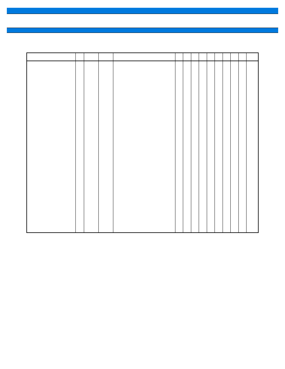
MB90220 Series
98
Table 21 Branch 2 Instructions [20 Instructions]
For an explanation of "(b)", "(c)" and "(d)", refer to Table 5, "Correction Values for Number of Cycles Used to Calculate
Number of Actual Cycles."
*1: 4 when branching, 3 when not branching
*2: 5 when branching, 4 when not branching
*3: 5 + (a) when branching, 4 + (a) when not branching
*4: 6 + (a) when branching, 5 + (a) when not branching
*5: 3
◊
(b) + 2
◊
(c) when an interrupt request is generated, 6
◊
(c) when returning from the interrupt.
*6: High-speed interrupt return instruction. When an interrupt request is detected during this instruction, the
instruction branches to the interrupt vector without performing stack operations when the interrupt is generated.
*7: Return from stack (word)
*8: Return from stack (long word)
Mnemonic
#
cycles
B
Operation
LH AH
I
S
T
N
Z
V
C
RMW
CBNE
A, #imm8, rel
CWBNE A, #imm16, rel
CBNE ear, #imm8, rel
CBNE eam, #imm8, rel
CWBNE ear, #imm16, rel
CWBNE eam, #imm16, rel
DBNZ
ear, rel
DBNZ
eam, rel
DWBNZ ear, rel
DWBNZ eam, rel
INT
#vct8
INT
addr16
INTP
addr24
INT9
RETI
RETIQ *
6
LINK
#imm8
UNLINK
RET *
7
RETP *
8
3
4
4
4+
5
5+
3
3+
3
3+
2
3
4
1
1
2
2
1
1
1
*
1
*
1
*
1
*
3
*
1
*
3
*
2
*
4
*
2
*
4
14
12
13
14
9
11
6
5
4
5
0
0
0
(b)
0
(c)
0
2
◊
(b)
0
2
◊
(c)
8
◊
(c)
6
◊
(c)
6
◊
(c)
8
◊
(c)
6
◊
(c)
*
5
(c)
(c)
(c)
(d)
Branch when byte (A)
imm8
Branch when byte (A)
imm16
Branch when byte (ear)
imm8
Branch when byte (eam)
imm8
Branch when word (ear)
imm16
Branch when word (eam)
imm16
Branch when byte (ear) =
(ear) ≠ 1, and (ear)
0
Branch when byte (ear) =
(eam) ≠ 1, and (eam)
0
Branch when word (ear) =
(ear) ≠ 1, and (ear)
0
Branch when word (eam) =
(eam) ≠ 1, and (eam)
0
Software interrupt
Software interrupt
Software interrupt
Software interrupt
Return from interrupt
Return from interrupt
At constant entry, save old
frame pointer to stack, set new
frame pointer, and allocate
local pointer area
At constant entry, retrieve old
frame pointer from stack.
Return from subroutine
Return from subroutine
≠
≠
≠
≠
≠
≠
≠
≠
≠
≠
≠
≠
≠
≠
≠
≠
≠
≠
≠
≠
≠
≠
≠
≠
≠
≠
≠
≠
≠
≠
≠
≠
≠
≠
≠
≠
≠
≠
≠
≠
≠
≠
≠
≠
≠
≠
≠
≠
≠
≠
R
R
R
R
*
*
≠
≠
≠
≠
≠
≠
≠
≠
≠
≠
≠
≠
≠
≠
S
S
S
S
*
*
≠
≠
≠
≠
≠
≠
≠
≠
≠
≠
≠
≠
≠
≠
≠
≠
≠
≠
*
*
≠
≠
≠
≠
*
*
*
*
*
*
*
*
*
*
≠
≠
≠
≠
*
*
≠
≠
≠
≠
*
*
*
*
*
*
*
*
*
*
≠
≠
≠
≠
*
*
≠
≠
≠
≠
*
*
*
*
*
*
*
*
*
*
≠
≠
≠
≠
*
*
≠
≠
≠
≠
*
*
*
*
*
*
≠
≠
≠
≠
≠
≠
≠
≠
*
*
≠
≠
≠
≠
≠
≠
≠
≠
≠
≠
≠
*
≠
*
≠
≠
≠
≠
≠
≠
≠
≠
≠
≠
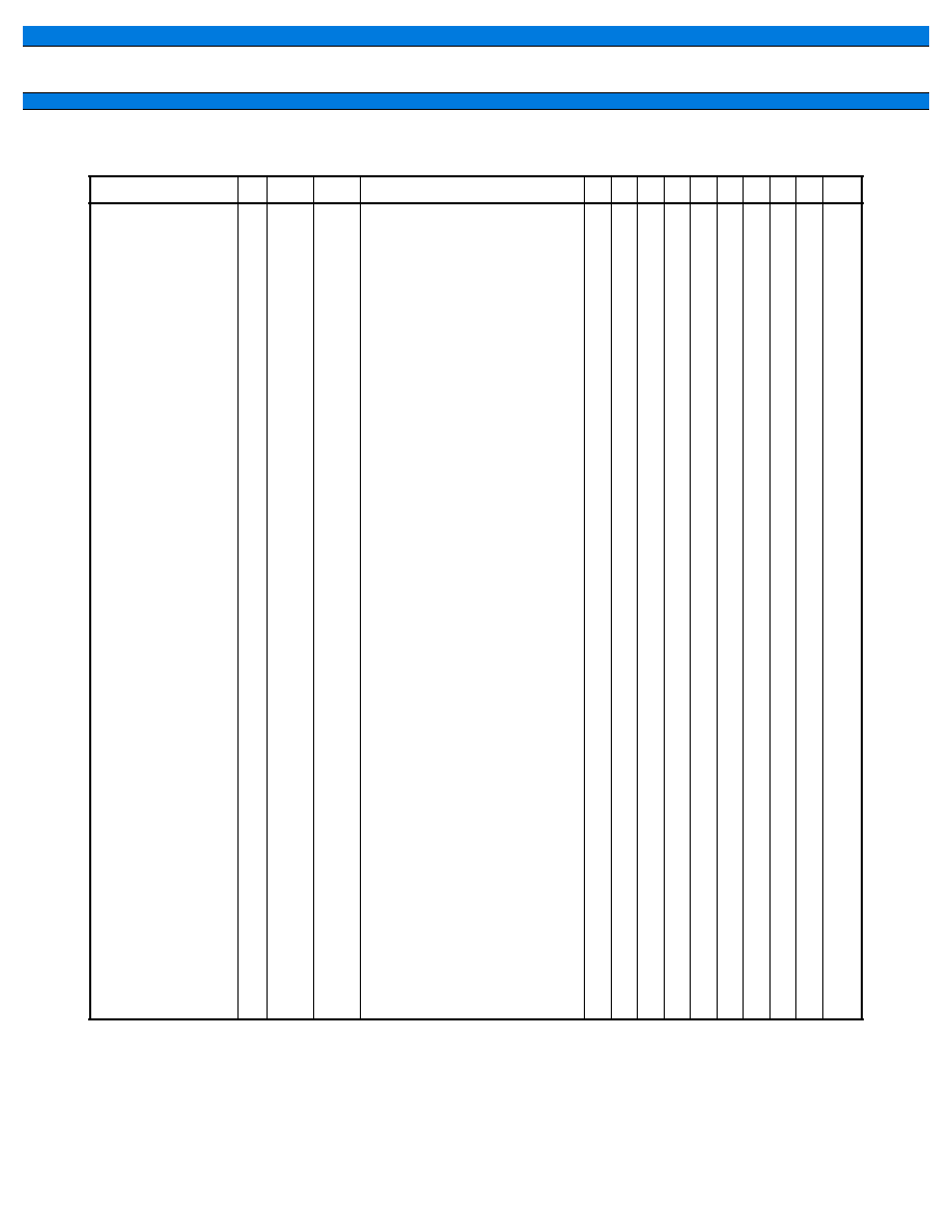
99
MB90220 Series
Table 22 Other Control Instructions (Byte/Word/Long Word) [36 Instructions]
For an explanation of "(a)" and "(c)", refer to Tables 4 and 5.
*1: PCB, ADB, SSB, USB, and SPB: 1 cycle
*4: Pop count
◊
(c), or push count
◊
(c)
DTB: 2 cycles
*5: 3 when AL is 0, 5 when AL is not 0.
DPR: 3 cycles
*6: 4 when AL is 0, 6 when AL is not 0.
*2: 3 + 4
◊
(pop count)
*7: 5 when AL is 0, 7 when AL is not 0.
*3: 3 + 4
◊
(push count)
Mnemonic
#
cycles
B
Operation
LH AH
I
S
T
N
Z
V
C
RMW
PUSHW A
PUSHW AH
PUSHW PS
PUSHW rlst
POPW A
POPW AH
POPW PS
POPW rlst
JCTX
@A
AND
CCR, #imm8
OR
CCR, #imm8
MOV RP, #imm8
MOV ILM, #imm8
MOVEA RWi, ear
MOVEA RWi, eam
MOVEA A, ear
MOVEA A, eam
ADDSP #imm8
ADDSP #imm16
MOV A, brgl
MOV brg2, A
MOV brg2, #imm8
NOP
ADB
DTB
PCB
SPB
NCC
CMR
MOVW SPCU, #imm16
MOVW SPCL, #imm16
SETSPC
CLRSPC
BTSCN
A
BTSCNS A
BTSCND A
1
1
1
2
1
1
1
2
1
2
2
2
2
2
2+
2
2+
2
3
2
2
3
1
1
1
1
1
1
1
4
4
2
2
2
2
2
3
3
3
*
3
3
3
3
*
2
9
3
3
2
2
3
2+ (a)
2
1+ (a)
3
3
*
1
1
2
1
1
1
1
1
1
1
2
2
2
2
*
5
*
6
*
7
(c)
(c)
(c)
*
4
(c)
(c)
(c)
*
4
6
◊
(c)
0
0
0
0
0
0
0
0
0
0
0
0
0
0
0
0
0
0
0
0
0
0
0
0
0
0
0
word (SP)
(SP) ≠2, ((SP))
(A)
word (SP)
(SP) ≠2, ((SP))
(AH)
word (SP)
(SP) ≠2, ((SP))
(PS)
(SP)
(SP) ≠2n, ((SP))
(rlst)
word (A)
((SP)), (SP)
(
SP) +2
word (AH)
((SP)), (SP)
(
SP) +2
word (PS)
((SP)), (SP)
(
SP) +2
(rlst)
((SP)) , (SP)
(SP)
Context switch instruction
byte (CCR)
(CCR) and imm8
byte (CCR)
(CCR) or imm8
byte (RP)
imm8
byte (ILM)
imm8
word (RWi)
ear
word (RWi)
eam
word(A)
ear
word (A)
eam
word (SP)
ext (imm8)
word (SP)
imm16
byte (A)
(brgl)
byte (brg2)
(A)
byte (brg2)
imm8
No operation
Prefix code for AD space access
Prefix code for DT space access
Prefix code for PC space access
Prefix code for SP space access
Prefix code for no flag change
Prefix code for the common
register bank
word (SPCU)
(imm16)
word (SPCL)
(imm16)
Stack check ooperation enable
Stack check ooperation disable
byte (A)
position of "1" bit in word (A)
byte (A)
position of "1" bit in word (A)
◊
2
byte (A)
position of "1" bit in word (A)
◊
4
≠
≠
≠
≠
≠
≠
≠
≠
≠
≠
≠
≠
≠
≠
≠
≠
≠
≠
≠
Z
≠
≠
≠
≠
≠
≠
≠
≠
≠
≠
≠
≠
≠
Z
Z
Z
≠
≠
≠
≠
*
≠
≠
≠
≠
≠
≠
≠
≠
≠
≠
*
*
≠
≠
*
≠
≠
≠
≠
≠
≠
≠
≠
≠
≠
≠
≠
≠
≠
≠
≠
≠
≠
≠
≠
≠
≠
*
≠
*
*
*
≠
≠
≠
≠
≠
≠
≠
≠
≠
≠
≠
≠
≠
≠
≠
≠
≠
≠
≠
≠
≠
≠
≠
≠
≠
≠
≠
≠
≠
≠
≠
*
≠
*
*
*
≠
≠
≠
≠
≠
≠
≠
≠
≠
≠
≠
≠
≠
≠
≠
≠
≠
≠
≠
≠
≠
≠
≠
≠
≠
≠
≠
≠
≠
≠
≠
*
≠
*
*
*
≠
≠
≠
≠
≠
≠
≠
≠
≠
≠
≠
≠
≠
≠
≠
≠
≠
≠
≠
≠
≠
≠
≠
≠
≠
≠
≠
≠
≠
≠
≠
*
≠
*
*
*
≠
≠
≠
≠
≠
≠
≠
≠
*
*
*
≠
≠
≠
≠
≠
≠
≠
≠
≠
≠
≠
≠
≠
≠
≠
≠
≠
≠
≠
≠
*
≠
*
*
*
≠
≠
≠
≠
≠
≠
≠
≠
*
*
*
≠
≠
≠
≠
≠
≠
≠
≠
≠
≠
≠
*
*
*
≠
≠
≠
≠
≠
≠
*
≠
*
*
*
≠
≠
≠
≠
≠
≠
≠
≠
≠
≠
≠
≠
≠
≠
≠
≠
≠
≠
≠
≠
≠
≠
≠
≠
≠
≠
≠
≠
≠
≠
≠
*
≠
*
*
*
≠
≠
≠
≠
≠
≠
≠
≠
≠
≠
≠
≠
≠
≠
≠
≠
≠
≠
≠
≠
≠
≠
≠
≠
≠
≠
≠
≠
≠
≠
≠
≠
≠
≠
≠
≠
≠
≠
≠
≠
≠
≠
≠
≠
≠
≠
≠
≠
≠
≠
≠
≠
≠
≠
≠
≠
≠
≠
≠
≠
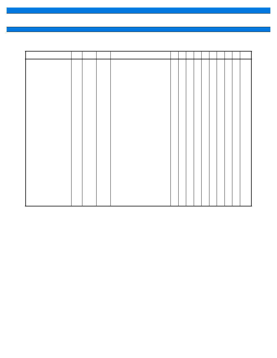
MB90220 Series
100
Table 23 Bit Manipulation Instructions [21 Instructions]
For an explanation of "(b)", refer to Table 5, "Correction Values for Number of Cycles Used to Calculate Number of
Actual Cycles."
*1: 5 when branching, 4 when not branching
*2: 7 when condition is satisfied, 6 when not satisfied
*3: Undefined count
*4: Until condition is satisfied
Mnemonic
#
cycles
B
Operation
LH AH
I
S
T
N
Z
V
C
RMW
MOVB
A, dir:bp
MOVB
A, addr16:bp
MOVB
A, io:bp
MOVB
dir:bp, A
MOVB
addr16:bp, A
MOVB
io:bp, A
SETB
dir:bp
SETB
addr16:bp
SETB
io:bp
CLRB
dir:bp
CLRB
addr16:bp
CLRB
io:bp
BBC
dir:bp, rel
BBC
addr16:bp, rel
BBC
io:bp, rel
BBS
dir:bp, rel
BBS
addr16:bp, rel
BBS
io:bp, rel
SBBS
addr16:bp, rel
WBTS
io:bp
WBTC io:bp
3
4
3
3
4
3
3
4
3
3
4
3
4
5
4
4
5
4
5
3
3
3
3
3
4
4
4
4
4
4
4
4
4
*
1
*
1
*
1
*
1
*
1
*
1
*
2
*
3
*
3
(b)
(b)
(b)
2
◊
(b)
2
◊
(b)
2
◊
(b)
2
◊
(b)
2
◊
(b)
2
◊
(b)
2
◊
(b)
2
◊
(b)
2
◊
(b)
(b)
(b)
(b)
(b)
(b)
(b)
2
◊
(b)
*
4
*
4
byte (A)
(dir:bp) b
byte (A)
(addr16:bp) b
byte (A)
(io:bp) b
bit (dir:bp) b
(A)
bit (addr16:bp) b
(A)
bit (io:bp) b
(A)
bit (dir:bp) b
1
bit (addr16:bp) b
1
bit (io:bp) b
1
bit (dir:bp) b
0
bit (addr16:bp) b
0
bit (io:bp) b
0
Branch when (dir:bp) b = 0
Branch when (addr16:bp) b = 0
Branch when (io:bp) b = 0
Branch when (dir:bp) b = 1
Branch when (addr16:bp) b = 1
Branch when (io:bp) b = 1
Branch when (addr16:bp) b = 1, bit = 1
Wait until (io:bp) b = 1
Wait until (io:bp) b = 0
Z
Z
Z
≠
≠
≠
≠
≠
≠
≠
≠
≠
≠
≠
≠
≠
≠
≠
≠
≠
≠
*
*
*
≠
≠
≠
≠
≠
≠
≠
≠
≠
≠
≠
≠
≠
≠
≠
≠
≠
≠
≠
≠
≠
≠
≠
≠
≠
≠
≠
≠
≠
≠
≠
≠
≠
≠
≠
≠
≠
≠
≠
≠
≠
≠
≠
≠
≠
≠
≠
≠
≠
≠
≠
≠
≠
≠
≠
≠
≠
≠
≠
≠
≠
≠
≠
≠
≠
≠
≠
≠
≠
≠
≠
≠
≠
≠
≠
≠
≠
≠
≠
≠
≠
*
*
*
*
*
*
≠
≠
≠
≠
≠
≠
≠
≠
≠
≠
≠
≠
≠
≠
≠
*
*
*
*
*
*
≠
≠
≠
≠
≠
≠
*
*
*
*
*
*
*
≠
≠
≠
≠
≠
≠
≠
≠
≠
≠
≠
≠
≠
≠
≠
≠
≠
≠
≠
≠
≠
≠
≠
≠
≠
≠
≠
≠
≠
≠
≠
≠
≠
≠
≠
≠
≠
≠
≠
≠
≠
≠
≠
≠
≠
≠
≠
*
*
*
*
*
*
*
*
*
≠
≠
≠
≠
≠
≠
*
≠
≠
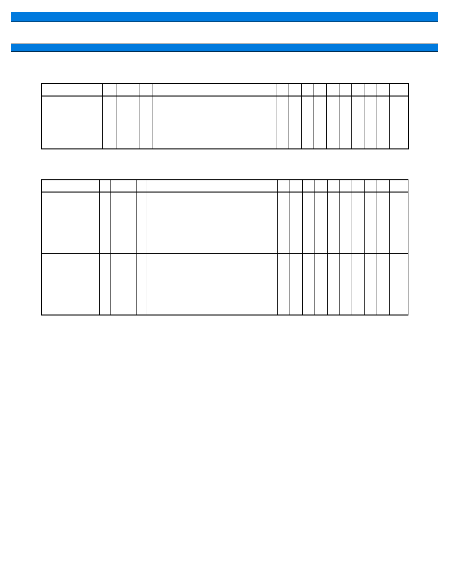
101
MB90220 Series
Table 24 Accumulator Manipulation Instructions (Byte/Word) [6 Instructions]
Table 25 String Instructions [10 Instructions]
m: RW0 value (counter value)
*1: 3 when RW0 is 0, 2 + 6
◊
(RW0) for count out, and 6n + 4 when match occurs
*2: 4 when RW0 is 0, 2 + 6
◊
(RW0) in any other case
*3: (b)
◊
(RW0)
*4: (b)
◊
n
*5: (b)
◊
(RW0)
*6: (c)
◊
(RW0)
*7: (c)
◊
n
*8: (c)
◊
(RW0)
Mnemonic
#
cycles
B
Operation
LH AH
I
S
T
N
Z
V
C
RMW
SWAP
SWAPW
EXT
EXTW
ZEXT
ZEXTW
1
1
1
1
1
1
3
2
1
2
1
2
0
0
0
0
0
0
byte (A) 0 to 7
(A) 8 to 15
word (AH)
(AL)
Byte code extension
Word code extension
Byte zero extension
Word zero extension
≠
≠
X
≠
Z
≠
≠
*
≠
X
≠
Z
≠
≠
≠
≠
≠
≠
≠
≠
≠
≠
≠
≠
≠
≠
≠
≠
≠
≠
≠
≠
*
*
R
R
≠
≠
*
*
*
*
≠
≠
≠
≠
≠
≠
≠
≠
≠
≠
≠
≠
≠
≠
≠
≠
≠
≠
Mnemonic
# cycles B
Operation
LH AH
I
S
T
N
Z
V
C
RMW
MOVS/MOVSI
MOVSD
SCEQ/SCEQI
SCEQD
FILS/FILSI
2
2
2
2
2
*
2
*
2
*
1
*
1
5m +3
*
3
*
3
*
4
*
4
*
5
Byte transfer @AH+
@AL+, counter = RW0
Byte transfer @AH≠
@AL≠, counter = RW0
Byte retrieval @AH+ ≠ AL, counter = RW0
Byte retrieval @AH≠ ≠ AL, counter = RW0
Byte filling @AH+
AL, counter = RW0
≠
≠
≠
≠
≠
≠
≠
≠
≠
≠
≠
≠
≠
≠
≠
≠
≠
≠
≠
≠
≠
≠
≠
≠
≠
≠
≠
*
*
*
≠
≠
*
*
*
≠
≠
*
*
≠
≠
≠
*
*
≠
≠
≠
≠
≠
≠
MOVSW/MOVSWI
MOVSWD
SCWEQ/SCWEQI
SCWEQD
FILSW/FILSWI
2
2
2
2
2
*
2
*
2
*
1
*
1
5m +3
*
6
*
6
*
7
*
7
*
8
Word transfer @AH+
@AL+, counter = RW0
Word transfer @AH≠
@AL≠, counter = RW0
Word retrieval @AH+ ≠ AL, counter = RW0
Word retrieval @AH≠ ≠ AL, counter = RW0
Word filling @AH+
AL, counter = RW0
≠
≠
≠
≠
≠
≠
≠
≠
≠
≠
≠
≠
≠
≠
≠
≠
≠
≠
≠
≠
≠
≠
≠
≠
≠
≠
≠
*
*
*
≠
≠
*
*
*
≠
≠
*
*
≠
≠
≠
*
*
≠
≠
≠
≠
≠
≠
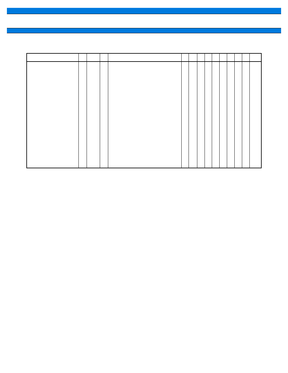
MB90220 Series
102
Table 26 Multiple Data Transfer Instructions [18 Instructions]
*1: 5 + imm8
◊
5, 256 times when imm8 is zero.
*2: 5 + imm8
◊
5 + (a), 256 times when imm8 is zero.
*3: Number of transfers
◊
(b)
◊
2
*4: Number of transfers
◊
(c)
◊
2
*5: The bank register specified by "bnk" is the same as for the MOVS instruction.
Mnemonic
#
cycles
B
Operation
LH AH
I
S
T N
Z
V C
RMW
MOVM @A, @RLi, #imm8
MOVM @A, eam, #imm8
MOVM addr16, @RLi, #imm8
MOVM addr16, eam, #imm8
MOVMW @A, @RLi, #imm8
MOVMW @A, eam, #imm8
MOVMW addr16, @RLi, #imm8
MOVMW addr16, eam, #imm8
MOVM @RLi, @A, #imm8
MOVM eam, @A, #imm8
MOVM @RLi, addr16, #imm8
MOVM eam, addr16, #imm8
MOVMW @RLi, @A, #imm8
MOVMW eam, @A, #imm8
MOVMW@RLi, addr16, #imm8
MOVMW eam, addr16, #imm8
MOVM bnk : addr16, *
5
bnk : addr16, #imm8
MOVMW bnk : addr16, *
5
bnk : addr16, #imm8
3
3+
5
5+
3
3+
5
5+
3
3+
5
5+
3
3+
5
5+
7
7
*
1
*
2
*
1
*
2
*
1
*
2
*
1
*
2
*
1
*
2
*
1
*
2
*
1
*
2
*
1
*
2
*
1
*
1
*
3
*
3
*
3
*
3
*
4
*
4
*
4
*
4
*
3
*
3
*
3
*
3
*
4
*
4
*
4
*
4
*
3
*
4
Multiple data trasfer byte ((A))
((RLi))
Multiple data trasfer byte ((A))
(eam)
Multiple data trasfer byte (addr16)
((RLi))
Multiple data trasfer byte (addr16)
(eam)
Multiple data trasfer word ((A))
((RLi))
Multiple data trasfer word ((A))
(eam)
Multiple data trasfer word (addr16)
((RLi))
Multiple data trasfer word (addr16)
(eam)
Multiple data trasfer byte ((RLi))
((A))
Multiple data trasfer byte (eam)
((A))
Multiple data transfer byte ((RLi))
(addr16)
Multiple data transfer byte (eam)
(addr16)
Multiple data trasfer word ((RLi))
((A))
Multiple data trasfer word (eam)
((A))
Multiple data transfer word ((RLi))
(addr16)
Multiple data transfer word (eam)
(addr16)
Multiple data transfer
byte (bnk:addr16)
(bnk:addr16)
Multiple data transfer
word (bnk:addr16)
(bnk:addr16)
≠
≠
≠
≠
≠
≠
≠
≠
≠
≠
≠
≠
≠
≠
≠
≠
≠
≠
≠
≠
≠
≠
≠
≠
≠
≠
≠
≠
≠
≠
≠
≠
≠
≠
≠
≠
≠
≠
≠
≠
≠
≠
≠
≠
≠
≠
≠
≠
≠
≠
≠
≠
≠
≠
≠
≠
≠
≠
≠
≠
≠
≠
≠
≠
≠
≠
≠
≠
≠
≠
≠
≠
≠
≠
≠
≠
≠
≠
≠
≠
≠
≠
≠
≠
≠
≠
≠
≠
≠
≠
≠
≠
≠
≠
≠
≠
≠
≠
≠
≠
≠
≠
≠
≠
≠
≠
≠
≠
≠
≠
≠
≠
≠
≠
≠
≠
≠
≠
≠
≠
≠
≠
≠
≠
≠
≠
≠
≠
≠
≠
≠
≠
≠
≠
≠
≠
≠
≠
≠
≠
≠
≠
≠
≠
≠
≠
≠
≠
≠
≠
≠
≠
≠
≠
≠
≠
≠
≠
≠
≠
≠
≠
≠
≠
≠
≠
≠
≠
≠
≠
≠
≠
≠
≠
≠
≠
≠
≠
≠
≠
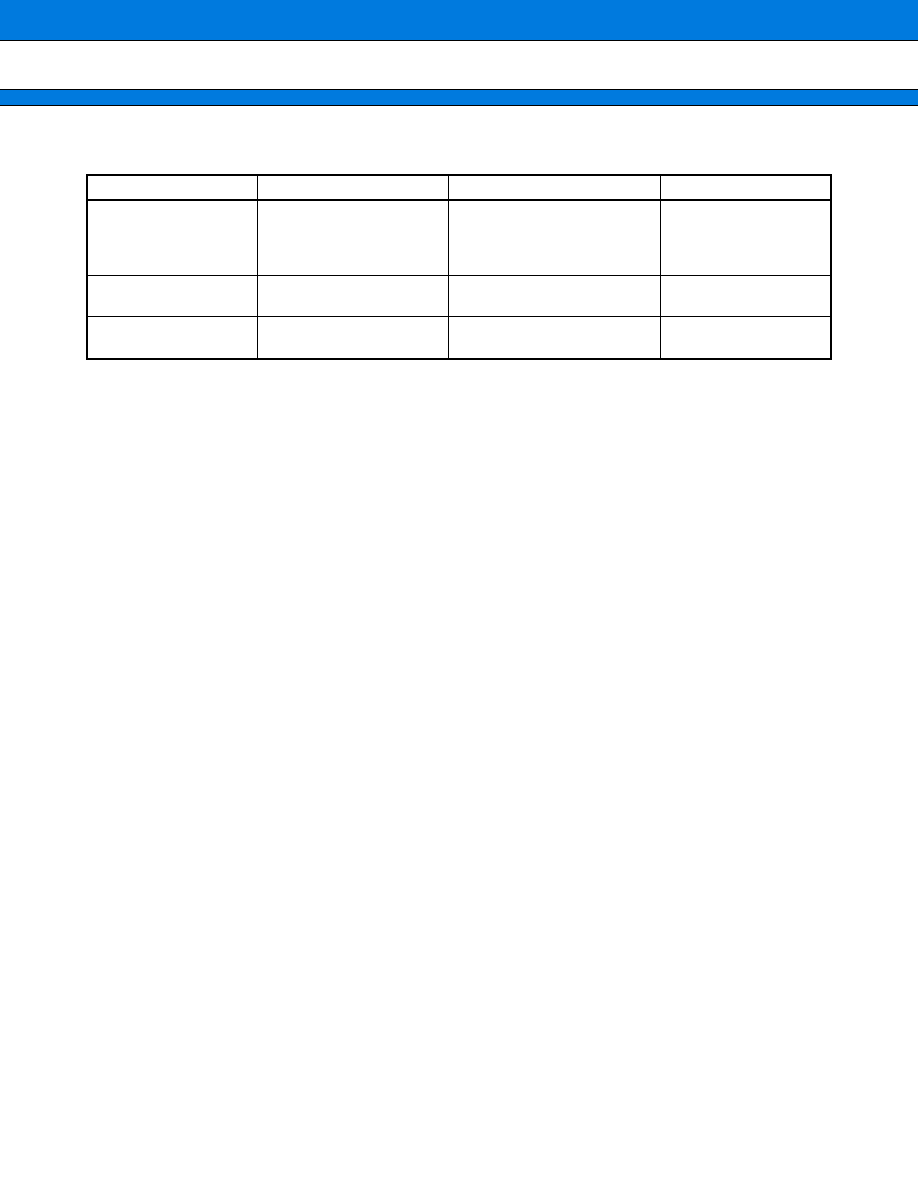
101
MB90220 Series
s
ORDERING INFORMATION
Part number
Type
Package
Remarks
MB90224
MB90223
MB90P224A
MB90P224B
MB90224PF
MB90223PF
MB90P224PF
MB90P224BPF
120-pin Plastic QFP
(FPT-120P-M03)
MB90W224A
MB90W224B
MB90W224ZF
MB90W224BZF
120-pin Ceramic QFP
(FPT-120C-C02)
ES level only
MB90V220
MB90V220CR
256-pin Ceramic PGA
(PGA-256C-A02)
For evaluation
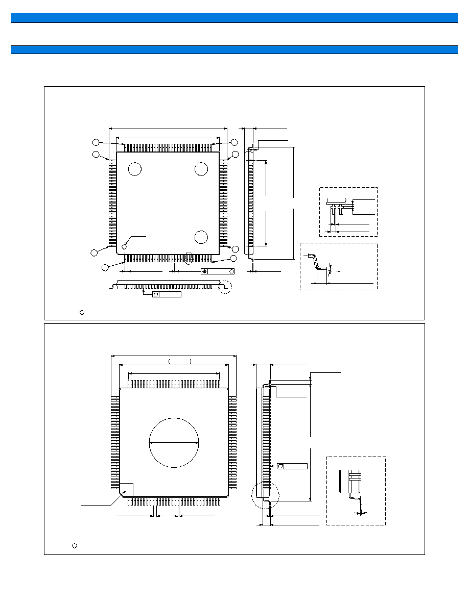
MB90220 Series
104
s
PACKAGE DIMENSIONS
Note: See to the latest version of Package Data Book for official package dimensions.
+0.60
≠0.30
+.023
≠.012
"A"
1.45±0.20(.057±.008)
0.15±0.05(.006±.002)
Details of "A" part
0∞~10∞
0∞
(STAND OFF)
0.05(.002)MIN
3.55(.140)MAX
(.0315±.008)
0.80±0.20
0.10(.004)
SQ
(1.197±.010)
30.40±0.25
INDEX AREA
(.0138±.0040)
0.35±0.10
0.80(.0315)TYP
ÿ12.70(.0500)REF
32.00±0.30(1.260±.012)SQ
SQ
28.00
1.102
23.20(.9135)REF
1994 FUJITSU LIMITED F120023SC-1-1
C
0.20(.008)
0.25(.010)
0.18(.007)MAX
0.58(.023)MAX
90
91
61
60
120
INDEX
31
30
LEAD No.
1
0.10(.004)
M
0.16(.006)
(.014±.004)
0.35±0.10
0.80(.0315)TYP
(.006±.002)
0.15±0.05
REF
(.913)
23.20
(1.197±.016)
30.40±0.40
(STAND OFF)
0(0)MIN
3.85(.152)MAX
28.00±0.20(1.102±.008)SQ
32.00±0.40(1.260±.016)SQ
"B"
"A"
0 10∞
0.80±0.20(.031±.008)
Details of "B" part
Details of "A" part
1994 FUJITSU LIMITED F120004S-3C-2
C
Dimensions in mm (inches)
120-pin Plastic QFP
(FPT-120P-M03)
120-pin Ceramic QFP
(FPT-120C-C02)
Dimensions in mm (inches)

105
MB90220 Series
FUJITSU LIMITED
For further information please contact:
Japan
FUJITSU LIMITED
Corporate Global Business Support Division
Electronic Devices
KAWASAKI PLANT, 4-1-1, Kamikodanaka
Nakahara-ku, Kawasaki-shi
Kanagawa 211-88, Japan
Tel: (044) 754-3763
Fax: (044) 754-3329
http://www.fujitsu.co.jp/
North and South America
FUJITSU MICROELECTRONICS, INC.
Semiconductor Division
3545 North First Street
San Jose, CA 95134-1804, U.S.A.
Tel: (408) 922-9000
Fax: (408) 922-9179
Customer Response Center
Mon. - Fri.: 7 am - 5 pm (PST)
Tel: (800) 866-8608
Fax: (408) 922-9179
http://www.fujitsumicro.com/
Europe
FUJITSU MIKROELEKTRONIK GmbH
Am Siebenstein 6-10
D-63303 Dreieich-Buchschlag
Germany
Tel: (06103) 690-0
Fax: (06103) 690-122
http://www.fujitsu-ede.com/
Asia Pacific
FUJITSU MICROELECTRONICS ASIA PTE LTD
#05-08, 151 Lorong Chuan
New Tech Park
Singapore 556741
Tel: (65) 281-0770
Fax: (65) 281-0220
http://www.fmap.com.sg/
F9710
©
FUJITSU LIMITED Printed in Japan
All Rights Reserved.
The contents of this document are subject to change without
notice. Customers are advised to consult with FUJITSU sales
representatives before ordering.
The information and circuit diagrams in this document presented
as examples of semiconductor device applications, and are not
intended to be incorporated in devices for actual use. Also,
FUJITSU is unable to assume responsibility for infringement of
any patent rights or other rights of third parties arising from the
use of this information or circuit diagrams.
FUJITSU semiconductor devices are intended for use in
standard applications (computers, office automation and other
office equipment, industrial, communications, and measurement
equipment, personal or household devices, etc.).
CAUTION:
Customers considering the use of our products in special
applications where failure or abnormal operation may directly
affect human lives or cause physical injury or property damage,
or where extremely high levels of reliability are demanded (such
as aerospace systems, atomic energy controls, sea floor
repeaters, vehicle operating controls, medical devices for life
support, etc.) are requested to consult with FUJITSU sales
representatives before such use. The company will not be
responsible for damages arising from such use without prior
approval.
Any semiconductor devices have inherently a certain rate of
failure. You must protect against injury, damage or loss from
such failures by incorporating safety design measures into your
facility and equipment such as redundancy, fire protection, and
prevention of over-current levels and other abnormal operating
conditions.
If any products described in this document represent goods or
technologies subject to certain restrictions on export under the
Foreign Exchange and Foreign Trade Control Law of Japan, the
prior authorization by Japanese government should be required
for export of those products from Japan.