
DS07-13606-1E
FUJITSU SEMICONDUCTOR
DATA SHEET
16-bit Proprietary Microcontroller
CMOS
F
2
MC-16L MB90620A Series
MB90622A/623A/P623A
s
DESCRIPTION
The MB90620A series is a line of general-purpose, 16-bit microcontrollers designed for those applications which
require high-speed real-time processing, proving to be suitable for various industrial machines, camera and
video devices, OA equipment, and for process control. The CPU used in this series is the F
2
MC*-16L. The
instruction set for the F
2
MC-16L CPU core is designed to be optimized for controller applications while inheriting
the AT architecture of the F
2
MC-16/16H series, allowing a wide range of control tasks to be processed efficiently
at high speed.
The peripheral resources integrated in the MB90620A series include: the UART (clock asynchronous/
synchronous transfer)
�
1 channel, the extended serial I/O interface
�
1 channel, the A/D converter (8/10-bit
precision)
�
4 channels, the 16-bit PPG timer (PWM/single-shot function)
�
2 channels, the 16-bit reload timer
�
3 channels, the 16-bit free-run timer (built-in compare register: 2 channels)
�
2 channels, the external interrupt
�
8 channels, the watch timer
�
1 channel, LCD controller/driver 32 segments
�
4 commons.
*: F
2
MC stands for FUJITSU Flexible Microcontroller.
s
FEATURES
F
2
MC-16L CPU
� Minimum execution time: 83.33 ns (at machine clock frequency of 12 MHz)
� Dual-clock control systems
� PLL clock control
(Continued)
s
PACKAGE
100-pin Plastic LQFP
(FPT-100P-M05)

MB90620A Series
2
(Continued)
� Instruction set optimized for controller applications
Variety of data types: bit, byte, word, long-word
Expanded addressing modes: 23 types
High coding efficiency
Improvement of high-precision arithmetic operations through use of 32-bit accumulator
� Instruction set supports high-level language (C language) and multitasking
Inclusion of system stack pointer
Enhanced pointer-indirect instructions
Barrel shift instruction
� Improved execution speed: 4-byte instruction queue
� 8-level, 32-factor powerful interrupt service functions
� Automatic transfer function independent of CPU (EI
2
OS)
� General-purpose ports: max. 59 channels
� 18-bit timebase timer/15-bit watch timer
� Watchdog timer function
� CPU intermittent operation function
� Various standby modes
Peripheral blocks
� ROM:32 Kbytes (MB90622A)
48 Kbytes (MB90623A)
� One-time PROM: 48 Kbytes (MB90P623A)
� RAM: 1.64 Kbytes (MB90622A)
2 Kbytes (MB90623A/P623A)
� General-purpose ports: max. 59 channels
� Dual-clock control system
� PLL clock multiplication control system
� UART: 1 channel
Can be used for either asynchronous transfer or synchronous transfer with clock
� Extended serial I/O interface: 1 channel
Can be used for 8-bit synchronous transfer
� A/D converter (8/10-bit resolution): 4 channels
� PPG (Programable pulse generator): 2 channels
� 16-bit reload timer: 3 channels
� 16-bit free-run timer: 2 channels
With compare register 2 channels
� LCD controller/driver
32 segments, 4 commons
� External interrupts: 8 channels
� 18-bit timebase timer
� 15-bit watch timer
� Watchdog timer function
� CPU intermittent operation function
� Standby mode
Watch mode
Sleep mode
Stop mode
3
MB90620A Series
s
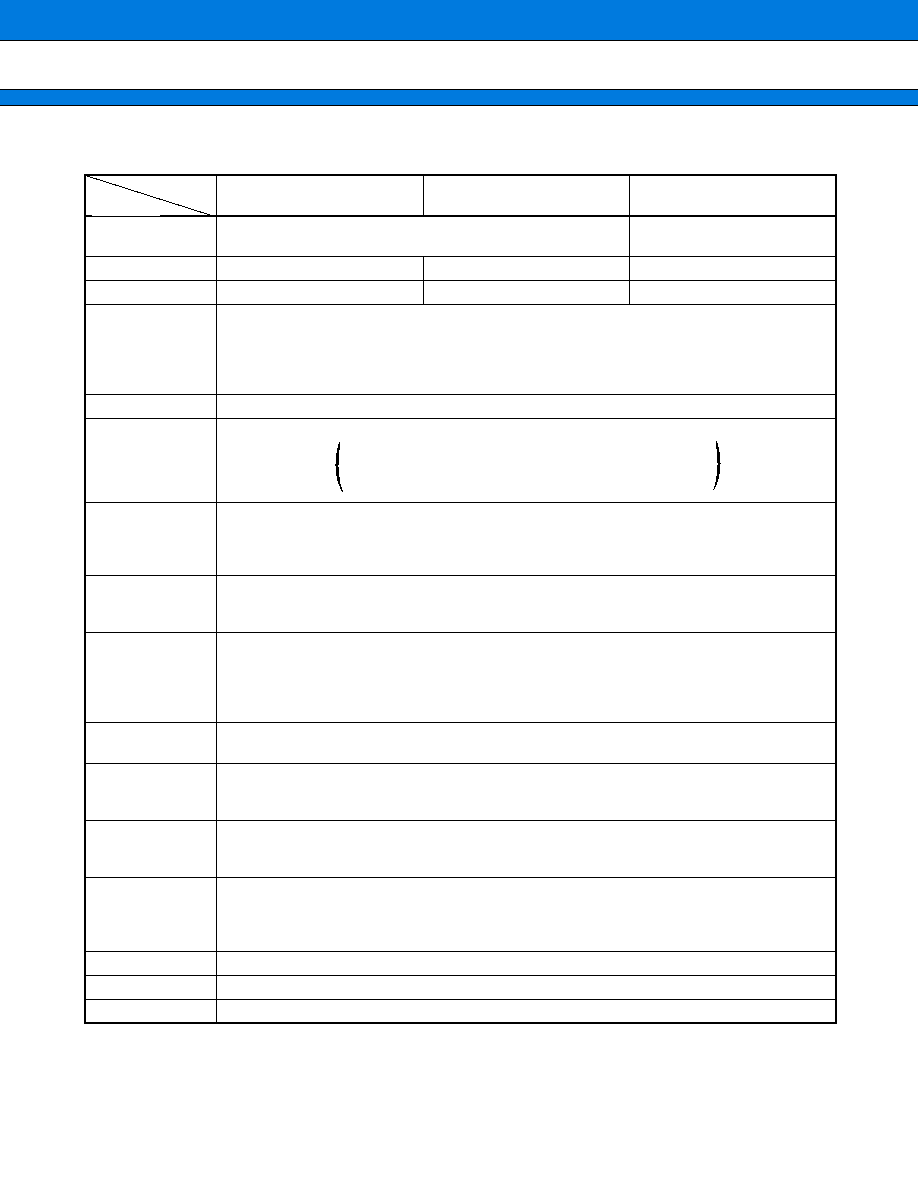
PRODUCT LINEUP
MB90623A
MB90P623A
Classification
Mass production products
(Mask ROM products)
One-time model
ROM size
32 Kbytes
48 Kbytes
48 Kbytes
RAM size
1.64 Kbytes
2 Kbytes
2 Kbytes
CPU functions
Number of instructions: 340
Instruction bit length: 8 or 16 bits
Instruction length: 1 to 7 bytes
Data bit length: 1, 4, 8, 16, or 32 bits
Minimum execution time: 83.33 ns at 12 MHz (internal)
Oscillation circuit
Dual-clock system of main clock and sub clock
Ports
UART
Number of channels: 1
Clock synchronous communication (1202 to 9615 bps, full-duplex double buffering)
Clock asynchronous communication (62.5 K to 1 M bps, full-duplex double buffering)
Supports multiprocessor mode
Serial
Number of channels: 1
Internal or external clock mode
Clock synchronous transfer (62.5 kHz to 1 MHz, "LSB first" or "MSB first" transfer)
A/D converter
Resolution: 10 or 8 bits, Number of input channels: 4
Single-conversion mode (conversion for a specified input channel)
Scan conversion mode (continuous conversion for specified consecutive channels)
Continuous conversion mode (repeated conversion for a specified channel)
Stop conversion mode (periodical conversion)
Timer
Number of channels: 3
16-bit reload timer operation (operation clock: SUB/2,
/2
3
,
/2
5
, external)
Free-run timer
Number of channels: 2
16-bit up-counter (four types of count clocks)
2 channels on each timer of the compare register (compare matching interrupt available)
PPG timer
Number of channels: 2
PWM function, single-shot function
With external trigger function
LCD controller
/driver
Common output: 4 channels, Segment output: 32 channels
Direct driving of the LCD module
16 bytes of data memory for display
Operation clock source (main clock/sub clock selective)
Standby modes
Stop mode, sleep mode, and watch mode
PLL functions
Main clock multiplication (
�
1,
�
2,
�
3 and
�
4)
Package
FPT-100P-M05
MB90622A
Max. 59 channels
I/O ports (CMOS): 17
I/O ports (CMOS) with pull-up resistor available: 24
I/O ports (open drain): 18
Parameter
Part number
MB90620A Series
4
s
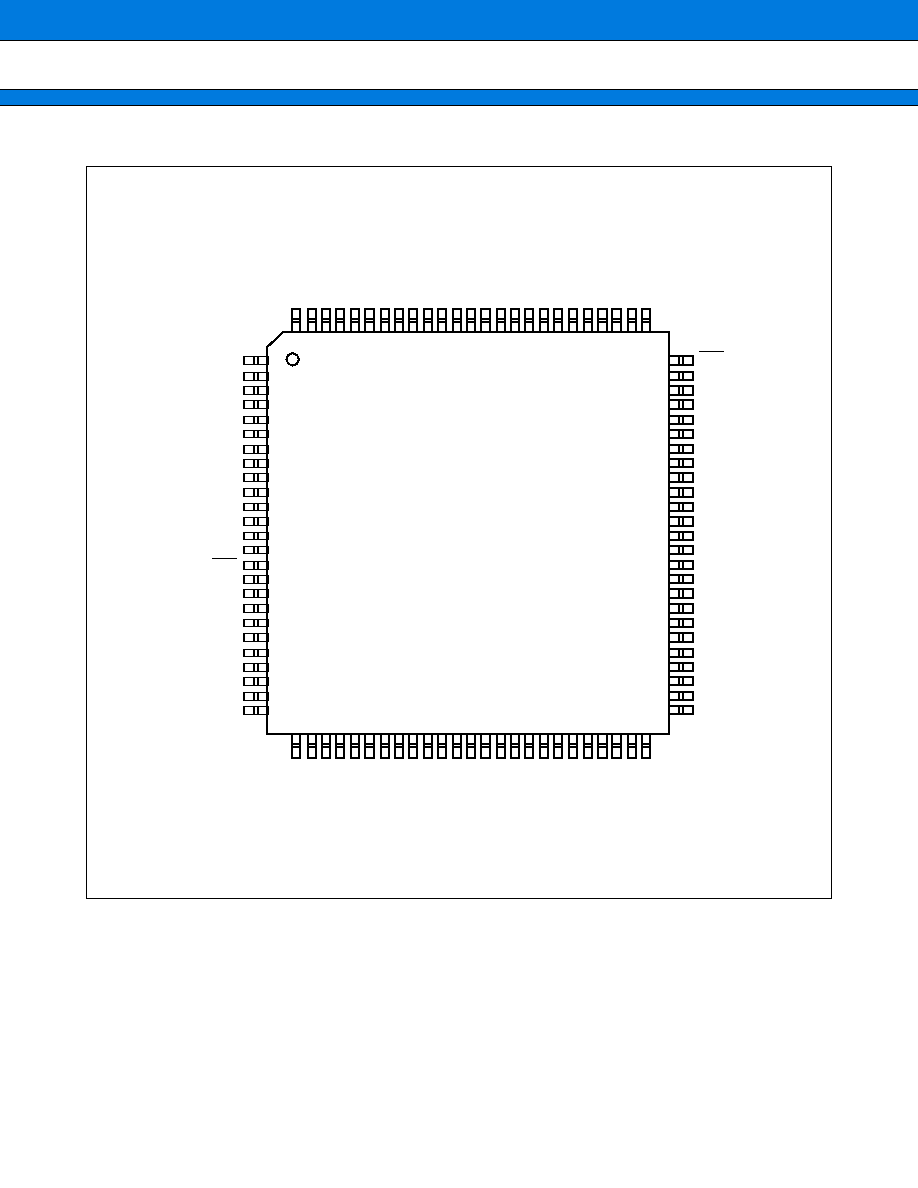
PIN ASSIGNMENT
75
74
73
72
71
70
69
68
67
66
65
64
63
62
61
60
59
58
57
56
55
54
53
52
51
RST
P76/SEG30
P75/SEG29
P74/SEG28
P73/SEG27
P72/SEG26
P71/SEG25
P70/SEG24
P67/SEG23
P66/SEG22
P65/SEG21
P64/SEG20
P63/SEG19
P62/SEG18
P61/SEG17
P60/SEG16
SEG15
SEG14
SEG13
SEG12
SEG11
SEG10
SEG09
SEG08
SEG07
1
2
3
4
5
6
7
8
9
10
11
12
13
14
15
16
17
18
19
20
21
22
23
24
25
P22
P23
P24/SIN0
P25/SOT0
P26/SCK0
P27/CKOT
P30/SIN1
P31/SOT1
V
SS
P32/SCK1
P33
P34
P35
P36
P37/TRG/ATG
P40/PPG0
P41/PPG1
P42/INT7/TIO0
P43/TIO1
P44/TIO2
V
CC
P45
P46
V0
V1
V2
V3
COM0
COM1
COM2
COM3
AV
CC
AVRH
AVRL
AV
SS
P50/AN0
P51/AN1
P52/AN2
P53/AN3
V
SS
SEG00
SEG01
SEG02
SEG03
SEG04
SEG05
MD0
MD1
MD2
SEG06
P21
P20
P17
P16
P15
P14
P13
P12
P11
P10
P07
P06/INT6
P05/INT5
P04/INT4
P03/INT3
P02/INT2
P01/INT1
P00/INT0
V
CC
X1
X0
V
SS
X0A
X1A
SEG31/P77
(Top view)
26
27
28
29
30
31
32
33
34
35
36
37
38
39
40
41
42
43
44
45
46
47
48
49
50
100
99
98
97
96
95
94
93
92
91
90
89
88
87
86
85
84
83
82
81
80
79
78
77
76
(FPT-100P-M05)
5
MB90620A Series
s
PIN DESCRIPTION
(Continued)
Pin no.
Pin name
Circuit type
Function
77
78
X1A
X0A
A
(Oscillation)
Crystal oscillator pins (32 kHz)
79
V
SS
Power supply
Digital circuit power supply (GND) pin
80
81
X0
X1
A
(Oscillation)
Crystal/FAR oscillator pins (4 MHz)
82
V
CC
Power supply
Digital circuit power supply pin
83 to 89
P00 to P06
M
(CMOS/H)
General-purpose I/O ports
At this pin, a pull-up resistor is added in the input mode depending
on the settings of the pull-up resistor setting register.
INT0 to INT6
External interrupt request input pins
When external interrupts are enabled, these inputs may be used at
any time; therefore, it is necessary to stop output by other functions
on these pins, except when using them for output deliberately.
90
P07
G
(CMOS)
General-purpose I/O port
At this pin, a pull-up resistor is added in the input mode depending
on the settings of the pull-up resistor setting register.
91 to 98
P10 to P17
G
(CMOS)
General-purpose I/O ports
At this pin, a pull-up resistor is added in the input mode depending
on the settings of the pull-up resistor setting register.
99, 100
1, 2
P20 to P23
G
(CMOS)
General-purpose I/O ports
At this pin, a pull-up resistor is added in the input mode depending
on the settings of the pull-up resistor setting register.
3
P24
F
(CMOS/H)
General-purpose I/O port
At this pin, a pull-up resistor is added in the input mode depending
on the settings of the pull-up resistor setting register.
SIN0
UART serial data input pin
During UART input operations, these inputs may be used at any
time; therefore, it is necessary to stop output by other functions on
these pins, except when using them for output deliberately.
4
P25
G
(CMOS)
General-purpose I/O port
At this pin, a pull-up resistor is added in the input mode depending
on the settings of the pull-up resistor setting register.
SOT0
UART serial data output pin
This function is available when the UART serial data output is
enabled.
5
P26
F
(CMOS/H)
General-purpose I/O port
At this pin, a pull-up resistor is added in the input mode depending
on the settings of the pull-up resistor setting register.
SCK0
UART serial data I/O pin
This function is available when the UART clock output is enabled.
During UART input operations, these inputs may be used at any
time; therefore, it is necessary to stop output by other functions on
these pins, except when using them for output deliberately.