DS07-13706-2E
FUJITSU SEMICONDUCTOR
DATA SHEET
16-bit Proprietary Microcontroller
CMOS
F
2
MC-16LX MB90550A/550B Series
MB90552A/552B/553A/553B/T552A/T553A
MB90F553A/P553A
s
s
s
s
DESCRIPTION
The MB90550A/550B series is a line of general-purpose, high-performance, 16-bit microcontrollers designed for
applications which require high-speed real-time processing, such as industrial machines, OA equipment, and
process control systems.
While inheriting the AT architecture of the F
2
MC*-8 family, the instruction set for the MB90550A/550B series
incorporates additional instructions for high-level languages, supports extended addressing modes, and contains
enhanced multiplication and division instructions as well as a substantial collection of improved bit manipulation
instructions. In addition, the MB90550A/550B has an on-chip 32-bit accumulator which enables processing of
long-word data.
MB90552B and MB90553B are radiation noise decreased type. There are no change in the functional specifica-
tion.
*: F
2
MC stands for FUJITSU Flexible Microcontroller, a registered trademark of FUJITSU LIMITED.
s
s
s
s
FEATURES
� Minimum instruction execution time: 62.5 ns (at oscillation of 4 MHz,
�
four times the
PLL clock)
� Maximum memory space: 16 Mbytes
� Instruction set optimized for controller applications
Supported data types: Bit, byte, word and long word
Typical addressing mode: 23 types
Enhanced precision calculation realized by 32-bit accumulator
Enhanced signed multiplication/division instruction and RETI instruction functions
(Continued)
s
s
s
s
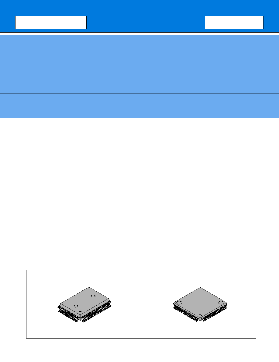
PACKAGES
100-pin plastic QFP
100-pin plastic LQFP
(FPT-100P-M06)
(FPT-100P-M05)

MB90550A/550B Series
2
(Continued)
� Instruction set designed for high level language (C) and multi-task operations
Adoption of system stack pointer
Symmetrical instruction set and barrel shift instructions
� Integrated address match detection function (for two address pointers)
� Faster execution speed: 4-byte queue
� Powerful interrupt functions (Eight priority levels programmable)
External interrupt inputs: 8 channels
� Data transfer functions (Intelligent I/O service): Up to 16 channels
DTP request inputs: 8 channels
� Embedded ROM size (EPROM, Flash: 128 Kbytes)
Mask ROM: 64 Kbytes/128 Kbytes
� Embedded RAM size (EPROM, Flash: 4 Kbytes)
Mask ROM: 2 Kbytes/4 Kbytes
� General-purpose ports: Up to 83 channels
(Input pull-up resistor settable for: 16 channels; Open drain settable for: 8 channels; I/O open drains: 6 chan-
nels)
� A/D converter (RC successive approximation type): 8 channels
(Resolution: 8 or 10 bits selectable; Conversion time of 26.3
�
s minimum)
� UART: 1 channel
� Extended I/O serial interface: 2 channels
� I
2
C interface: 2 channels
(Two channels, including one switchable between terminal input and output)
� 16-bit reload timer: 2 channels
� 8/16-bit PPG timer: 3 channels
(8 bits
�
2 channels; 16 bits x 1 channel: Mode switching function provided)
� 16-bit I/O timer
(Input capture
�
4 channels, output compare
�
4 channels, free run timer
�
1 channel)
� Clock monitor function integrated (Delivering the oscillation clock divided by 21 to 28)
� Timebase timer/watchdog timer: 18 bits
� Low power consumption modes (sleep, stop, hardware standby, and CPU intermittent operation modes)
� Package: QFP-100, LQFP-100
� CMOS technology
MB90550A/550B Series
3
s
s
s
s
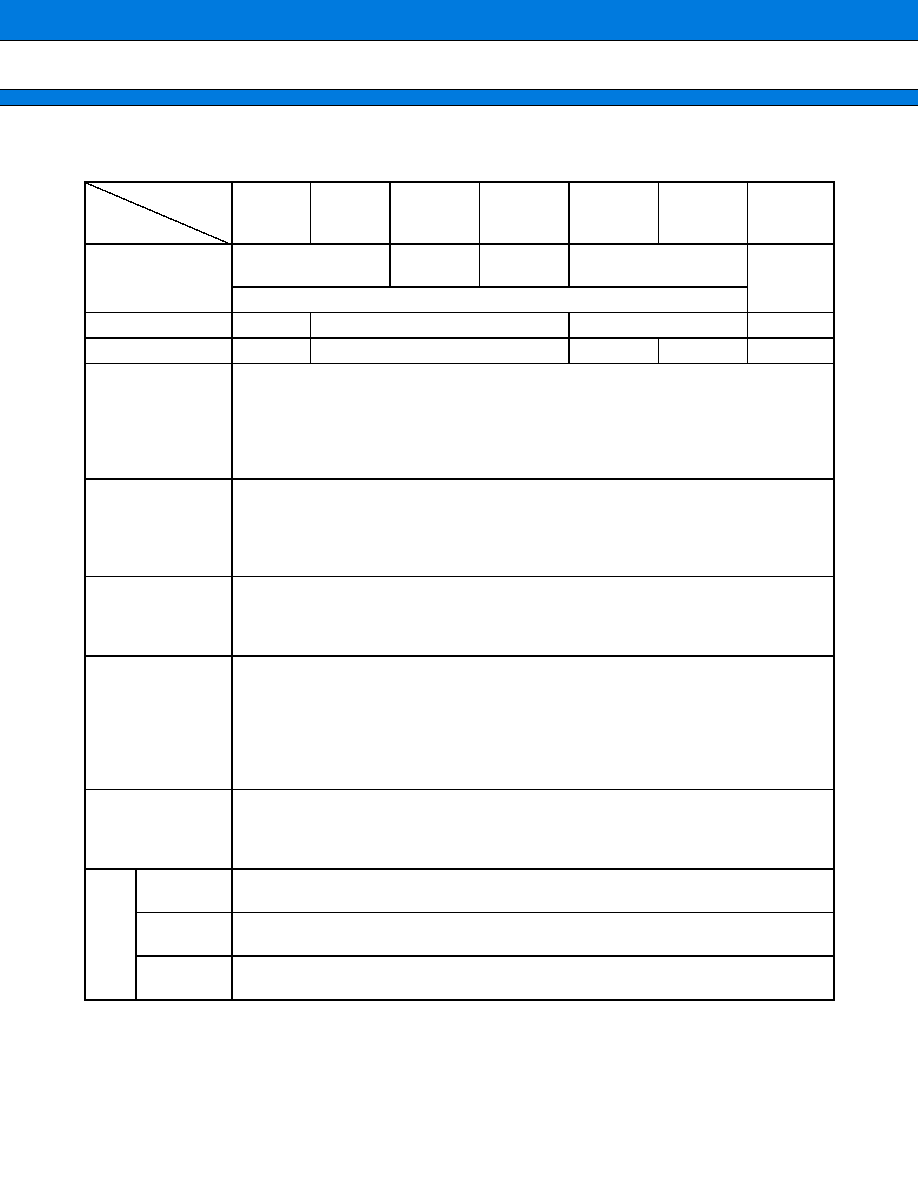
PRODUCT LINEUP
(Continued)
Part number
Item
MB90552A
MB90552B
MB90553A
MB90553B
MB90F553A
MB90P553A
MB90T552A
MB90T553A MB90V550A
Classification
Mask ROM products
Flash ROM
products
OTP
External ROM products
Evaluation
product
Mass Product
ROM size
64 Kbytes
128 Kbytes
None
None
RAM size
2 Kbytes
4 Kbytes
2 Kbytes
4 Kbytes
6 Kbytes
CPU functions
The number of instructions: 340
Instruction bit length: 8 bits, 16 bits
Instruction length: 1 byte to 7 bytes
Data bit length: 1 bit, 8 bits, 16 bits
Minimum execution time: 62.5 ns (at machine clock of 16 MHz)
Interrupt processing time: 1.5 ms (at machine clock of 16 MHz, minimum value)
Ports
General-purpose I/O ports (CMOS output): 53
General-purpose I/O ports (with pull-up resistor): 16
General-purpose I/O ports (N-channel open-drain output): 6
General-purpose I/O ports (N-channel open-drain function selectable): 8
Total: 83
UART (SCI)
Clock synchronized transmission (62.5 Kbps to 2 Mbps)
Clock asynchronized transmission (62500 bps to 9615 bps)
Transmission can be performed by bi-directional serial transmission or by
master/slave connection.
8/10-bit A/D
converter
Conversion precision: 8/10-bit can be selectively used.
Number of inputs: 8
One-shot conversion mode (converts selected channel only once)
Scan conversion mode (converts two or more successive channels and can program up to
8 channels.)
Continuous conversion mode (converts selected channel continuously)
Stop conversion mode (converts selected channel and stop operation repeatedly)
8/16-bit PPG timer
Number of channels: 1 (8-bit
�
2 channels)
PPG operation of 8-bit or 16-bit
A pulse wave of given intervals and given duty ratios can be output.
Pulse interval: 62.5 ns to 1 ms (at oscillation of 4 MHz, machine clock of 16 MHz)
16-bit
I/O
timer
16-bit
free run timer
Number of channels: 1
Overflow interrupts
Output com-
pare (OCU)
Number of channels: 4
Pin input factor: A match signal of compare register
Input capture
(ICU)
Number of channels: 4
Rewriting a register value upon a pin input (rising, falling or both edges)
MB90550A/550B Series
4
(Continued)
*:Varies with conditions such as the operating frequency. (See section "
s
ELECTRICAL CHARACTERISTICS")
Assurance for the MB90V550A is given only for operation with a tool at a power voltage of 4.5 V to 5.5 V, an
operating temperature of 0
�
C to +25
�
C, and an operating frequency of 1 MHz to 16 MHz.
s
s
s
s
PACKAGE AND CORRESPONDING PRODUCTS
: Available
�
: Not available
Note:For more information about each package, see section "
s
PACKAGE DIMENSIONS"
s
s
s
s
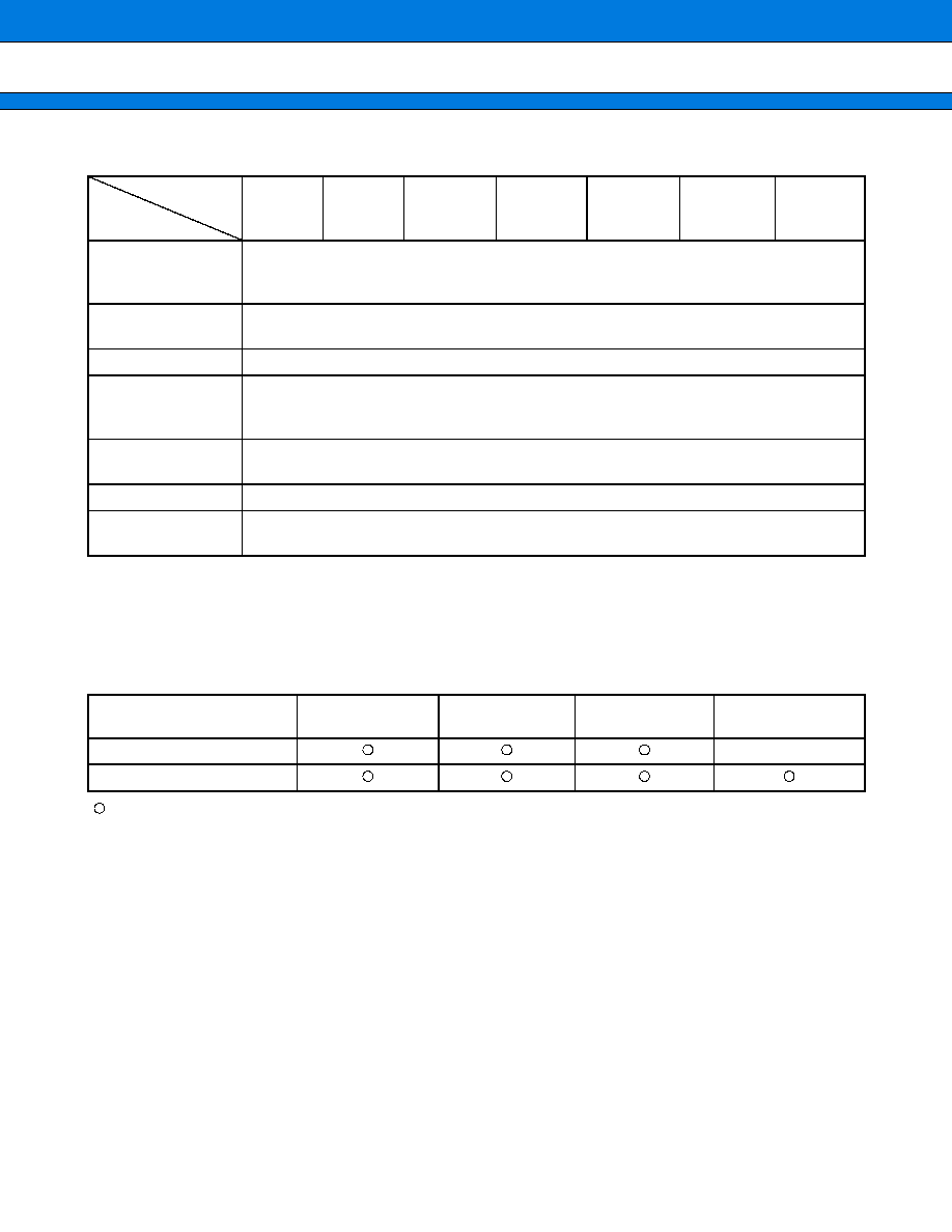
DIFFERENCES AMONG PRODUCTS
Memory Size
In evaluation with an evaluation product, note the difference between the evaluation product and the product
actually used. The following items must be taken into consideration.
� The MB90V550A does not have an internal ROM. However, operations equivalent to those performed by a
chip with an internal ROM can be evaluated by using a dedicated development tool, enabling selection of ROM
size by setting the development tool.
� In the MB90V550A, images from FF4000
H
to FFFFFF
H
are mapped to bank 00, and FE0000
H
to FF3FFF
H
are mapped to bank FE and FF only. (This setting can be changed by configuring the development tool.)
� In the MB90F553A/553A/553B/552A/552B, images from FF4000
H
to FFFFFF
H
are mapped to bank 00, and
FF0000
H
to FF3FFF
H
to bank FF only.
Part number
Item
MB90552A
MB90552B
MB90553A
MB90553B
MB90F553A MB90P553A MB90T552A
MB90T553A MB90V550A
DTP/external
interrupt circuit
Number of inputs: 8
Started by a rising edge, a falling edge, an "H" level input, or an "L" level input.
External interrupt circuit or extended intelligent I/O service (EI
2
OS) can be used.
Extended I/O serial
interface
Clock synchronized transmission (3125 bps to 1 Mbps)
LSB first/MSB first
I
2
C interface
Serial I/O port for supporting Inter IC BUS
Timebase timer
18-bit counter
Interrupt interval: 1.024 ms, 4.096 ms, 16.384 ms, 131.072 ms
(at oscillation of 4 MHz)
Watchdog timer
Reset generation interval: 3.58 ms, 14.33 ms, 57.23 ms, 458.75 ms
(at oscillation of 4 MHz, minimum value)
Process
CMOS
Power supply volt-
age for operation*
4.5 V to 5.5 V
Package
MB90552A
MB90552B
MB90553A
MB90553B
MB90F553A
MB90P553A
FPT-100P-M05
�
FPT-100P-M06
MB90550A/550B Series
5
s
s
s
s
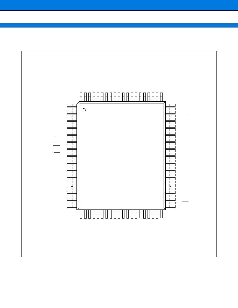
PIN ASSIGNMENTS
� FPT-100P-M06
(Top View)
(FPT-100P-M06)
80
79
78
77
76
75
74
73
72
71
70
69
68
67
66
65
64
63
62
61
60
59
58
57
56
55
54
53
52
51
1
2
3
4
5
6
7
8
9
10
11
12
13
14
15
16
17
18
19
20
21
22
23
24
25
26
27
28
29
30
100
99
98
97
96
95
94
93
92
91
90
89
88
87
86
85
84
83
82
81
31
32
33
34
35
36
37
38
39
40
41
42
43
44
45
46
47
48
49
50
P20/A16
P21/A17
P22/A18
P23/A19
P24/A20
P25/A21
P26/A22
P27/A23
P30/ALE
P31/RD
V
SS
P32/WRL
P33/WRH
P34/HRQ
P35/HAK
P36/RDY
P37/CLK
P40/SCK
P41/SOT
P42/SIN
P43/SCK1
P44/SOT1
V
CC
P45/SIN1
P46/ADTG
P47/SCK0
C
P50/SDA0/SOT0
P51/SCL0/SIN0
P52/SDA1
PA4/CKOT
PA2
RST
PA1/OUT3
PA0/OUT2
P97/PPG5
P96/PPG4
P95/PPG3
P94/PPG2
P93/PPG1
P92/PPG0
P91/OUT1
P92/OUT0
P87/IN3
P86/IN2
P85/IN1
P84/IN0
P83/TOT1
P82/TOT0
P81/TIN1
P80/TIN0
P77/IRQ7
P76/IRQ6
P75/IRQ5
P74/IRQ4
P73/IRQ3
P72/IRQ2
HST
MD2
PA3
P17/AD15
P16/AD14
P15/AD13
P14/AD12
P13/AD11
P12/AD10
P11/AD09
P10/AD08
P07/AD07
P06/AD06
P05/AD05
P04/AD04
P03/AD03
P02/AD02
P01/AD01
P00/AD00
V
CC
X1
X0
V
SS
P53/SCL1
P54/SDA2
P55/SCL2
P60/AN0
P61/AN1
P62/AN2
P63/AN3
V
SS
P64/AN4
P65/AN5
P66/AN6
P67/AN7
P70/IRQ0
P71/IRQ1
MD0
MD1
AV
CC
AVRH
AVRL
AV
SS