 | –≠–ª–µ–∫—Ç—Ä–æ–Ω–Ω—ã–π –∫–æ–º–ø–æ–Ω–µ–Ω—Ç: MB90xxxx | –°–∫–∞—á–∞—Ç—å:  PDF PDF  ZIP ZIP |
DS07-13603-5E
FUJITSU SEMICONDUCTOR
DATA SHEET
16-bit Proprietary Microcontroller
CMOS
F
2
MC-16L MB90610A Series
MB90611A/MB90613A
s
s
s
s
DESCRIPTION
MB90610A series includes 16-bit microcontrollers optimally usable for high-speed real-time data processing in
consumer appliances and for system control of printer, CD-ROM, cellular phone, copier, etc. The series uses the
F
2
MC*-16L CPU which is based on the F
2
MC-16 but with enhanced high-level language and task switching
instructions and additional addressing modes.
The internal peripheral resources consist of a 3-channel serial port incorporating a UART function (and supporting
I/O expansion serial mode), 8-channel 10-bit A/D converter, 2-channel PPG, 2-channel 16-bit reload timer, 8-
channel chip select output, and 8-channel external interrupts.
Also, multiplexed or non-multiplexed operation can be selected for the address/data bus.
*: F
2
MC is an abbreviation for "Fujitsu Flexible Microcontroller".
s
s
s
s
FEATURES
∑ F
2
MC-16L CPU
∑ Minimum instruction execution time:62.5 ns/4 MHz oscillation (Uses PLL clock multiplication),
maximum multiplier = 4
(Continued)
s
s
s
s
PACKAGES
100-pin plastic LQFP
(FPT-100P-M05)
100-pin plastic QFP
(FPT-100P-M06)

MB90610A Series
2
(Continued)
∑ Enhanced high level language (C) / multitasking support instructions
Use of a system stack pointer
Enhanced pointer indirect instructions
Barrel shift instructions
Stack check function
∑ Improved execution speed: Four byte instruction queue
∑ Powerful interrupt function
∑ Automatic data transfer function (does not use instructions)
Internal peripherals
∑ RAM: 1 Kbyte (MB90611A)3 Kbytes (MB90613A)
∑ General purpose ports8, 16-bit data bus, multiplexed mode:
57 ports max.
16-bit non-multiplexed mode:
41 ports max.
8-bit non-multiplexed mode:
49 ports max.
∑ UART (SCI): 3 channels
For either asynchronous or clocked serial transfer (I/O expansion serial)
∑ A/D converter: 8 channels (10-bit)
8-bit conversion mode also available
∑ PPG (programmable pulse generator): 2 channels
∑ 16-bit reload timer: 2 channels
∑ Chip select output: 8 channels
∑ External interrupts: 8 channels
∑ 18-bit timebase timer
Watchdog timer function
∑ PLL clock multiplier function
∑ CPU intermittent operation function
∑ Various standby modes
∑ LQFP-100/QFP-100 package
∑ CMOS technology
MB90610A Series
3
s
s
s
s
PRODUCT LINEUP
MB90611A
MB90613A
Classification
Mask ROM
ROM size
--
RAM size
1 Kbyte
3 Kbytes
CPU functions
Number of basic instructions:
340
Instruction bit length:
8/16 bits
Instruction length:
1 to 7 bytes
Data bit length:
1/4/8/16/32 bits
Minimum instruction execution time:62.5 ns/4 MHz (PLL multiplier = 4)
Interrupt processing time:
1000 ns/16 MHz (minimum)
Ports
I/O ports (CMOS/TTL): 33 (31 CMOS/2 TTL)
(N-channel open drain): 8 (16-bit non-multiplex mode)
Total:
41
Packages
FPT-100P-M05
FPT-100P-M06
UART
(SCI)
Three internal UARTs
Full-duplex, double-buffered
Selectable clock synchronous or asynchronous operation
Built-in dedicated baud rate generator
A/D Converter
10-bit
◊
8 channels
A/D conversion time:6.13
µ
s (98 machine cycles/16 MHz machine clock, includes sample
and hold time)
Triggers:
Software, external, or multi-function timer output (RT0) activation can
be selected.
Activation modes:
Single, scan (continuous conversion of multiple channels), continuous
(continuous conversion of one channel), and stop (scan mode with
synchronized conversion start)
PPG
2
◊
8-bit PPG outputs
(1 channel PPG output in 16-bit mode)
16-Bit Reload Tim-
er
16-bit reload timer operation (selectable toggle output, one-shot output)
(Selectable count clock: 0.125
µ
s, 0.5
µ
s, or 2.0
µ
s for a 16 MHz machine cycle)
Selectable event count function, 2 internal channels
Chip select
8 outputs
External interrupts
8 inputs
External interrupt mode (Interrupts can be generated from four different types of request
signal)
PLL Function
Selectable multiplier:1/2/3/4 (Set a multiplier that does not exceed the assured operation
frequency range.)
Other
--
Part No.
Parameter
MB90610A Series
4
s
s
s
s
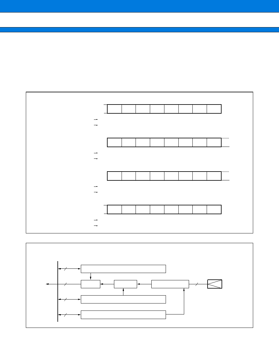
PIN ASSIGNMENT
(Continued)
75
74
73
72
71
70
69
68
67
66
65
64
63
62
61
60
59
58
57
56
55
54
53
52
51
RST
P54/WRH
P53/HRQ
P52/HAK
P51/RDY
P50/CLK
PA7/CS7
PA6/CS6
PA5/CS5
PA4/CS4
PA3/CS3
PA2/CS2
PA1/CS1
CS0
P95/SCK2
P94/SOT2
P93/SIN2
P92/SCK1
P91/SOT1
P90/SIN1
P86/SCK0
P85/SOT0
P84/SIN0
P83/TOT1
P82/TOT0
1
2
3
4
5
6
7
8
9
10
11
12
13
14
15
16
17
18
19
20
21
22
23
24
25
P22/A02
P23/A03
P24/A04
P25/A05
P26/A06
P27/A07
P30/A08
P31/A09
V
SS
P32/A10
P33/A11
P34/A12
P35/A13
P36/A14
P37/A15
P40/A16
P41/A17
P42/A18
P43/A19
P44/A20
V
CC
P45/A21
P46/A22
P47/A23
P70/INT0
P71/INT1
P72/INT2
P73/INT3
P74/INT4/PPG0
P75/INT5/PPG1
P76/INT6/ATG
AV
CC
AVRH
AVRL
AV
SS
P60/AN0
P61/AN1
P62/AN2
P63/AN3
V
SS
P64/AN4
P65/AN5
P66/AN6
P67/AN7
P80/INT7/TIN0
P81/TIN1
MD0
MD1
MD2
HST
P21/A01
P20/A00
P17/D15/AD15
P16/D14/AD14
P15/D13/AD13
P14/D12/AD12
P13/D11/AD11
P12/D10/AD10
P11/D09/AD09
P10/D08/AD08
D07/AD07
D06/AD06
D05/AD05
D04/AD04
D03/AD03
D02/AD02
D01/AD01
D00/AD00
V
CC
X1
X0
V
SS
ALE
RD
P55/WRL
(Top view)
26
27
28
29
30
31
32
33
34
35
36
37
38
39
40
41
42
43
44
45
46
47
48
49
50
100
99
98
97
96
95
94
93
92
91
90
89
88
87
86
85
84
83
82
81
80
79
78
77
76
(FPT-100P-M05)
MB90610A Series
5
(Continued)
80
79
78
77
76
75
74
73
72
71
70
69
68
67
66
65
64
63
62
61
60
59
58
57
56
55
54
53
52
51
ALE
RD
P55/WRL
RST
P54/WRH
P53/HRQ
P52/HAK
P51/RDY
P50/CLK
PA7/CS7
PA6/CS6
PA5/CS5
PA4/CS4
PA3/CS3
PA2/CS2
PA1/CS1
CS0
P95/SCK2
P94/SOT2
P93/SIN2
P92/SCK1
P91/SOT1
P90/SIN1
P86/SCK0
P85/SOT0
P84/SIN0
P83/TOT1
P82/TOT0
HST
MD2
1
2
3
4
5
6
7
8
9
10
11
12
13
14
15
16
17
18
19
20
21
22
23
24
25
26
27
28
29
30
P20/A00
P21/A01
P22/A02
P23/A03
P24/A04
P25/A05
P26/A06
P27/A07
P30/A08
P31/A09
V
SS
P32/A10
P33/A11
P34/A12
P35/A13
P36/A14
P37/A15
P40/A16
P41/A17
P42/A18
P43/A19
P44/A20
V
CC
P45/A21
P46/A22
P47/A23
P70/INT0
P71/INT1
P72/INT2
P73/INT3
P74/INT4/PPG0
P75/INT5/PPG1
P76/INT6/ATG
AV
CC
AVRH
AVRL
AV
SS
P60/AN0
P61/AN1
P62/AN2
P63/AN3
V
SS
P64/AN4
P65/AN5
P66/AN6
P67/AN7
P80/INT7/TIN0
P81/TIN1
MD0
MD1
P17/D15/AD15
P16/D14/AD14
P15/D13/AD13
P14/D12/AD12
P13/D11/AD11
P12/D10/AD10
P11/D09/AD09
P10/D08/AD08
D07/AD07
D06/AD06
D05/AD05
D04/AD04
D03/AD03
D02/AD02
D01/AD01
D00/AD00
V
CC
X1
X0
V
SS
(Top view)
31
32
33
34
35
36
37
38
39
40
41
42
43
44
45
46
47
48
49
50
100
99
98
97
96
95
94
93
92
91
90
89
88
87
86
85
84
83
82
81
(FPT-100P-M06)
MB90610A Series
6
s
s
s
s
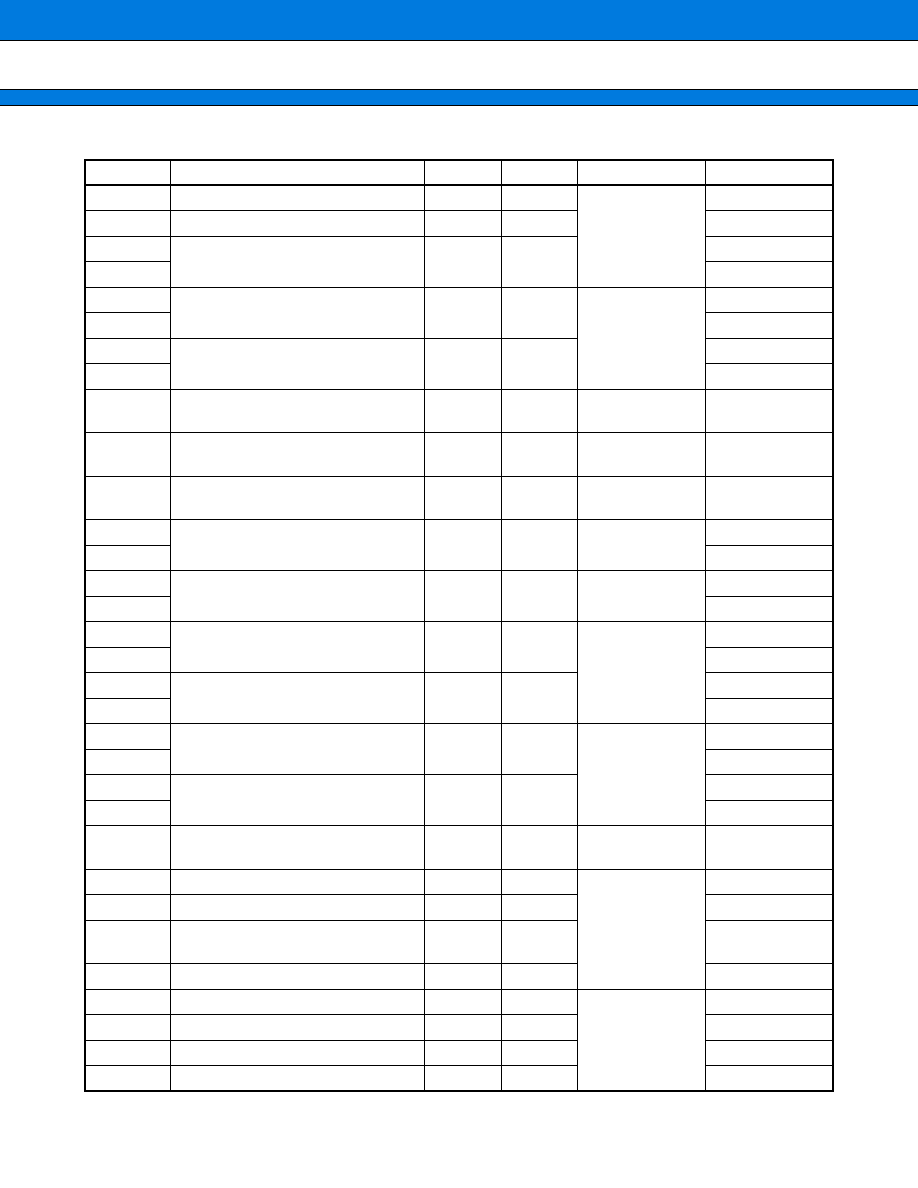
PIN DESCRIPTION
(Continued)
*1: FPT-100P-M05
*2: FPT-100P-M06
Pin no.
Pin name
Circuit
type
Function
LQFP*
1
QFP*
2
80
81
82
83
X0
X1
A
(Oscillator)
Crystal oscillator pins
83 to 90
85 to 92
D00 to D07
K
(TTL)
In non-multiplex mode, the I/O pins for the lower 8 bits of the
external data bus.
AD00 to AD07
In multiplexed mode, the I/O pins for the lower 8 bits of the ex-
ternal address/data bus.
91 to 98
93 to 100
P10 to P17
K
(TTL)
General purpose I/O ports
This applies in non-multiplexed mode with an 8-bit external
data bus.
P08 to D15
In non-multiplexed mode, the I/O pins for the upper 8 bits of
the external data bus
This applies when using a 16-bit external data bus.
AD08 to AD15
In multiplexed mode, the I/O pins for the upper 8 bits of the ex-
ternal address/data bus.
99
100
1 to 6
1 to 8
P20 to P27
B
(CMOS)
General purpose I/O ports
This applies in multiplexed mode.
A00 to A07
In non-multiplexed mode, the output pins for the lower 8 bits
of the external address bus.
7
8
10 to 15
9
10
12 to 17
P30 to P37
B
(CMOS)
General purpose I/O ports
This applies in multiplexed mode.
A08 to A15
In non-multiplexed mode, the output pins for the upper 8 bits
of the external address bus.
16 to 20
22 to 24
18 to 22
24 to 26
P40 to P47
B
(CMOS)
General purpose I/O ports
This applies when the upper address control register specifies
port operation.
A16 to A23
The output pins for A16 to 23 of the external address bus
This applies when the upper address control register specifies
address operation.
25 to 28
27 to 30
P70 to P73
H
(CMOS/H)
General purpose I/O ports
This applies in all cases.
INT0 to INT3
External interrupt request input pins
As the inputs operate continuously when external interrupts
are enabled, output to the pins from other functions must be
stopped unless done intentionally.
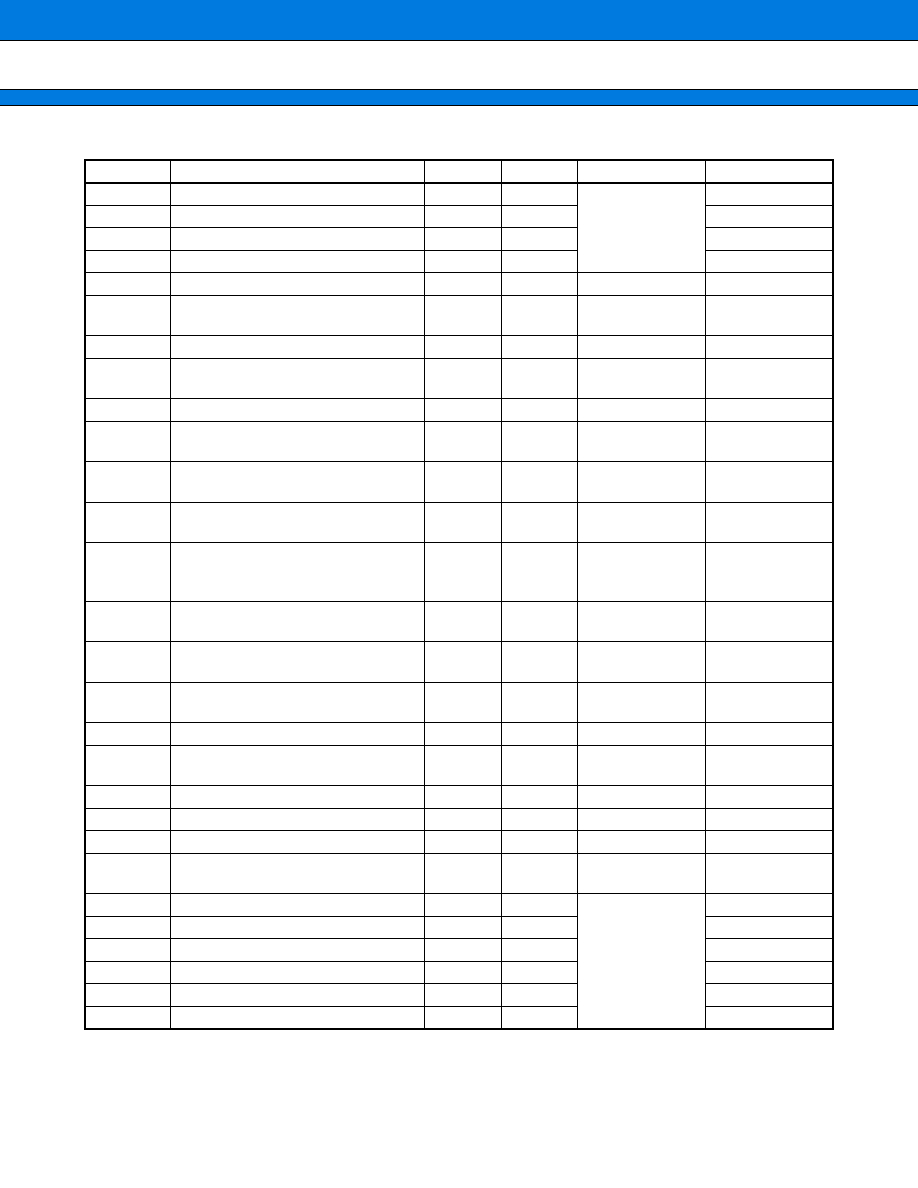
MB90610A Series
7
(Continued)
*1: FPT-100P-M05
*2: FPT-100P-M06
Pin no.
Pin name
Circuit
type
Function
LQFP*
1
QFP*
2
29
30
31
32
P74, P75
H
(CMOS/H)
General purpose I/O ports
This applies when the waveform outputs for PPG timers 0 to
1 are disabled.
INT4, INT5
External interrupt request input pins
As the inputs operate continuously when external interrupts
are enabled, output to the pins from other functions must be
stopped unless done intentionally.
PPG0, PPG1
Output pins for PPG timers 0 to 1
This applies when the waveform outputs for PPG timers 0 to
1 are enabled.
31
33
P76
H
(CMOS/H)
General purpose I/O port
This applies in all cases.
INT6
H
(CMOS/H)
External interrupt request input pin
As the input operates continuously when the external interrupt
is enabled, output to the pin from other functions must be
stopped unless done intentionally.
ATG
Trigger input pin for the A/D converter
As the input operates continuously when the A/D converter in-
puts are operating, output to the pin from other functions must
be stopped unless done intentionally.
32
34
AV
CC
Power
supply
Power supply for the analog circuits
Do not switch this power supply on/off unless a voltage great-
er than AV
CC
is applied to V
CC
.
33
35
AVRH
Power
supply
Analog circuit reference voltage input
Do not switch the voltage to this pin on/off unless a voltage
greater than AVRH is applied to AV
CC
.
34
36
AVRL
Power
supply
Analog circuit reference voltage input
35
37
AV
SS
Power
supply
Ground level for the analog circuits
36 to 39
41 to 44
38 to 41
43 to 46
P60 to P67
C
(AD)
Open-drain output ports
This applies when port operation is specified in the analog in-
put enable register.
AN0 to AN7
Analog input pins for the A/D converter
This applies when analog input mode operation is specified in
the analog input enable register.
45
47
P80
H
(CMOS/H)
General purpose I/O port
This applies in all cases.
INT7
External interrupt request input pin
As the input operates continuously when the external interrupt
is enabled, output to the pin from other functions must be
stopped unless done intentionally.
TIN0
Event input pin for reload timer 0
As the input operates continuously when the reload timer is
set to input operation, output to the pin from other functions
must be stopped unless done intentionally.
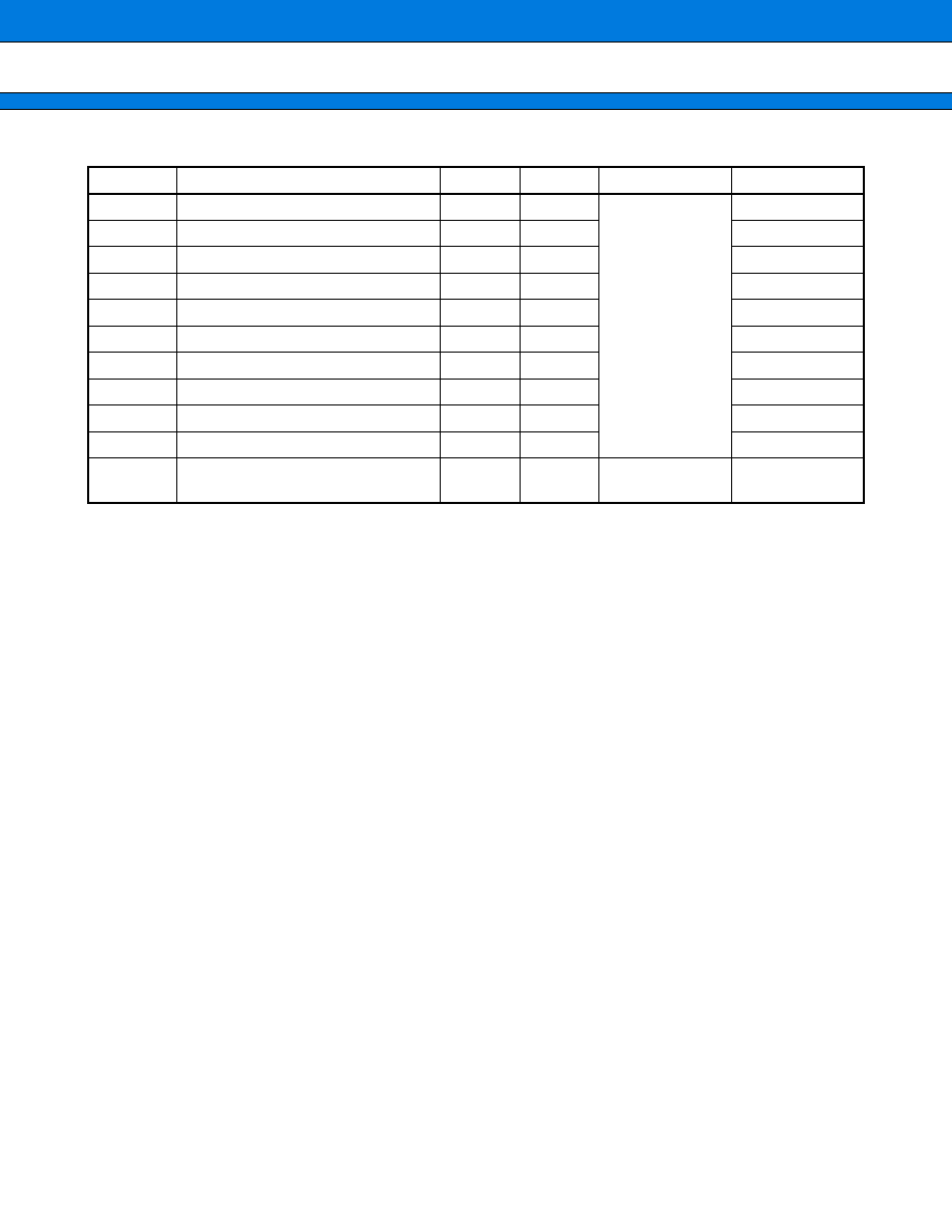
MB90610A Series
8
(Continued)
*1: FPT-100P-M05
*2: FPT-100P-M06
Pin no.
Pin name
Circuit
type
Function
LQFP*
1
QFP*
2
46
48
P81
D
(CMOS/H)
General purpose I/O port
This applies in all cases.
TIN1
Event input pin for reload timer 1
As the input operates continuously when the reload timer is set
to input operation, output to the pin from other functions must
be stopped unless done intentionally.
47,
48
49,
50
MD0, MD1
E
(CMOS/H)
Input pins for specifying an operating mode
Connect directly to V
CC
or V
SS
.
49
51
MD2
M
(CMOS/H)
Input pins for specifying an operating mode
Connect directly to V
CC
or V
SS
.
50
52
HST
F
(CMOS/H)
Hardware standby input pin
51, 52
53, 54
P82, P83
D
(CMOS/H)
General purpose I/O ports
This applies when output is disabled for reload timers 0 to 1.
TOT0, TOT1
Output pins for reload timers 0 to 1
This applies when output is enabled for reload timers 0 to 1.
53
55
P84
D
(CMOS/H)
General purpose I/O port
This applies in all cases.
SIN0
Serial data input pin for UART0
As the input operates continuously when UART0 is set to input
operation, output to the pin from other functions must be
stopped unless done intentionally.
54
56
P85
D
(CMOS/H)
General purpose I/O port
This applies when serial data output is disabled for UART0.
SOT0
Serial data output pin for UART0
This applies when serial data output is enabled for UART0.
55
57
P86
D
(CMOS/H)
General purpose I/O port
This applies when the UART0 clock output is disabled.
SCK0
Clock I/O pin for UART0
This applies when the UART0 clock output is enabled.
As the input operates continuously when UART0 is set to input
operation, output to the pin from other functions must be
stopped unless done intentionally.
56
58
P90
D
(CMOS/H)
General purpose I/O port
This applies in all cases.
SIN1
Serial data input pin for UART1
As the input operates continuously when UART1 is set to input
operation, output to the pin from other functions must be
stopped unless done intentionally.

MB90610A Series
9
(Continued)
*1: FPT-100P-M05
*2: FPT-100P-M06
Pin no.
Pin name
Circuit
type
Function
LQFP*
1
QFP*
2
57
59
P91
D
(CMOS/H)
General purpose I/O port
This applies when serial data output is disabled for UART1.
SOT1
Serial data output pin for UART1
This applies when serial data output is enabled for UART1.
58
60
P92
D
(CMOS/H)
General purpose I/O port
This applies when the UART1 clock output is disabled.
SCK1
Clock I/O pin for UART1
This applies when the UART1 clock output is enabled.
As the input operates continuously when UART1 is set to in-
put operation, output to the pin from other functions must be
stopped unless done intentionally.
59
61
P93
D
(CMOS/H)
General purpose I/O port
This applies in all cases.
SIN2
Serial data input pin for UART2
As the input operates continuously when UART2 is set to in-
put operation, output to the pin from other functions must be
stopped unless done intentionally.
60
62
P94
D
(CMOS/H)
General purpose I/O port
This applies when serial data output is disabled for UART2.
SOT2
Serial data output pin for UART2
This applies when serial data output is enabled for UART2.
61
63
P95
D
(CMOS/H)
General purpose I/O port
This applies when the UART2 clock output is disabled.
SCK2
Clock I/O pin for UART2
This applies when the UART2 clock output is enabled.
As the input operates continuously when UART2 is set to in-
put operation, output to the pin from other functions must be
stopped unless done intentionally.
62
64
CS0
J
(CMOS)
Chip select pin for program ROM
63 to 69
65 to 71
PA1 to PA7
I
(CMOS)
General purpose I/O ports
This applies for pins with chip select output disabled by the
chip select control register.
CS1 to CS7
Output pins for the chip select function
This applies for pins with chip select output enabled by the
chip select control register.
70
72
P50
I
(CMOS)
General purpose I/O port
This applies when CLK output is enabled.
CLK
CLK output pin
MB90610A Series
10
(Continued)
*1: FPT-100P-M05
*2: FPT-100P-M06
Pin no.
Pin name
Circuit
type
Function
LQFP*
1
QFP*
2
71
73
P51
L
(TTL)
General purpose I/O port
This applies when the external ready function is disabled.
RDY
Ready input pin
This applies when the external ready function is enabled.
72
74
P52
I
(CMOS)
General purpose I/O port
This applies when the hold function is disabled.
HAK
Hold acknowledge output pin
This applies when the hold function is enabled.
73
75
P53
L
(TTL)
General purpose I/O port
This applies when the hold function is disabled.
HRQ
Hold request input pin
This applies when the hold function is enabled.
74
76
P54
I
(CMOS)
General purpose I/O port
This applies in 8-bit external bus mode or when output is dis-
abled for the WR pin.
WRH
Write strobe output pin for the upper 8 bits of the data bus This
applies in 16-bit external bus mode and when output is en-
abled for the WR pin.
75
77
RST
G
(CMOS/H)
External reset request input pin
76
78
P55
I
(CMOS)
General purpose I/O port
This applies when output is disabled for the WR pin.
WRL
Write strobe output pin for the lower 8 bits of the data bus This
applies when output is enabled for the WR pin.
77
79
RD
J
(CMOS)
Read strobe output pin for the data bus
78
80
ALE
J
(CMOS)
ALE (address latch enabling) output pin
21, 82
23, 84
V
CC
Power
supply
Power supply for the digital circuits
9, 40, 79
11, 42,
81
V
SS
Power
supply
Ground level for the digital circuits
MB90610A Series
11
s
s
s
s
I/O CIRCUIT TYPE
Note: For pins with pull-up resistors, the resistance is disconnected when the pin outputs the "L" level or when in
the standby state.
(Continued)
Type
Circuit
Remarks
A
∑ Max. 3 to 32 MHz
∑ Oscillator feedback resistance:approximately
1 M
B
∑ CMOS level I/O
With standby control
C
∑ N-channel open drain output
∑ CMOS level hysteresis input
With AD control
D
∑ CMOS level output
∑ CMOS level hysteresis input
With standby control
X1
X0
Standby control
Clock input
Standby control
Digital input
Digital output
Digital output
R
A/D Disable
Digital input
Digital output
A/D input
R
Standby control
Digital input
Digital output
Digital output
R
MB90610A Series
12
Note: For pins with pull-up resistors, the resistance is disconnected when the pin outputs the "L" level or when in
the standby state.
(Continued)
Type
Circuit
Remarks
E
∑ CMOS level input
No standby control
F
∑ CMOS level hysteresis input
No standby control
G
∑ CMOS level hysteresis input
No standby control
∑ With pull-up
H
∑ CMOS level output
∑ CMOS level hysteresis input
No standby control
I
∑ CMOS level I/O
∑ Pull-up resistor approximately 50 k
∑ Pin goes to high impedance during stop
mode.
Digital input
R
Digital input
R
Digital input
R
Digital output
Digital output
Digital input
R
Standby control
Digital input
Digital output
Digital output
R
Standby control
MB90610A Series
13
(Continued)
Note: For pins with pull-up resistors, the resistance is disconnected when the pin outputs the "L" level or when in
the standby state.
Type
Circuit
Remarks
J
∑ CMOS level output
∑ Pull-up resistor approximately 50 k
∑ Pin goes to high impedance during stop
mode.
K
∑ CMOS level output
∑ TTL level input
With standby control
L
∑ CMOS level output
∑ TTL level input
∑ Pull-up resistor approximately 50 k
∑ Pin goes to high impedance during stop
mode.
M
∑ CMOS level input
No standby control
Digital output
Digital output
Standby control
Standby control
Digital input
Digital output
Digital output
R
Standby control
Digital input
Digital output
Digital output
R
Standby control
Digital input
R
MB90610A Series
14
s
s
s
s
HANDLING DEVICES
1.
Preventing Latchup
Latchup occurs in a CMOS IC if a voltage greater than V
CC
or less than V
SS
is applied to an input or output pin
or if the voltage applied between V
CC
and V
SS
exceeds the rating.
If latchup occurs, the power supply current increases rapidly resulting in thermal damage to circuit elements.
Therefore, ensure that maximum ratings are not exceeded in circuit operation.
For the same reason, also ensure that the analog supply voltage does not exceed the digital supply voltage.
2.
Treatment of Unused Pins
Leaving unused input pins unconnected can cause misoperation. Always pull-up or pull-down unused pins.
3.
External Reset Input
To reliably reset the controller by inputting an "L" level to the RST pin, ensure that the "L" level is applied for at
least five machine cycles. Take particular note when using an external clock input.
4.
V
CC
and V
SS
Pins
Ensure that all V
CC
pins are at the same voltage. The same applies for the V
SS
pins.
5.
Cautions When Using an External Clock
Drive the X0 pin only when using an external clock.
6.
A/D Converter Power Supply and the Turn-on Sequence for Analog Inputs
Always cut the A/D converter power supply (AV
CC
, AVRH, AVRL) and analog inputs (AN0 to AN7) before discon-
necting the digital power supply (V
CC
).
When turning the power on or off, ensure that AVRH does not exceed AV
CC
.
Also, when using the analog input pins as input ports, ensure that the input voltage does not exceed AV
CC
.
X0
X1
MB90610A Series
OPEN
∑ Using an External Clock
MB90610A Series
15
s
s
s
s
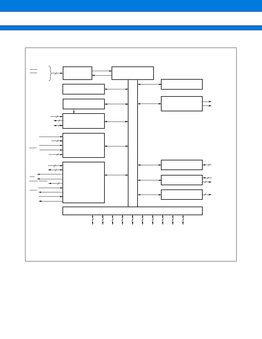
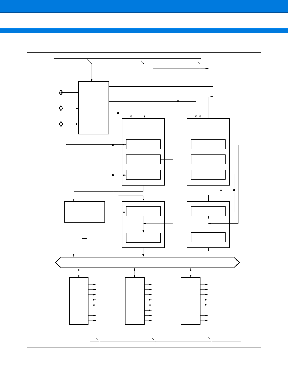
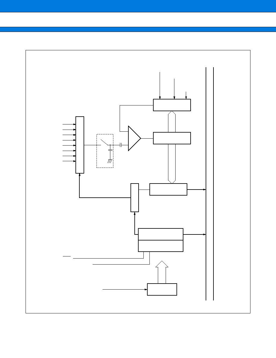
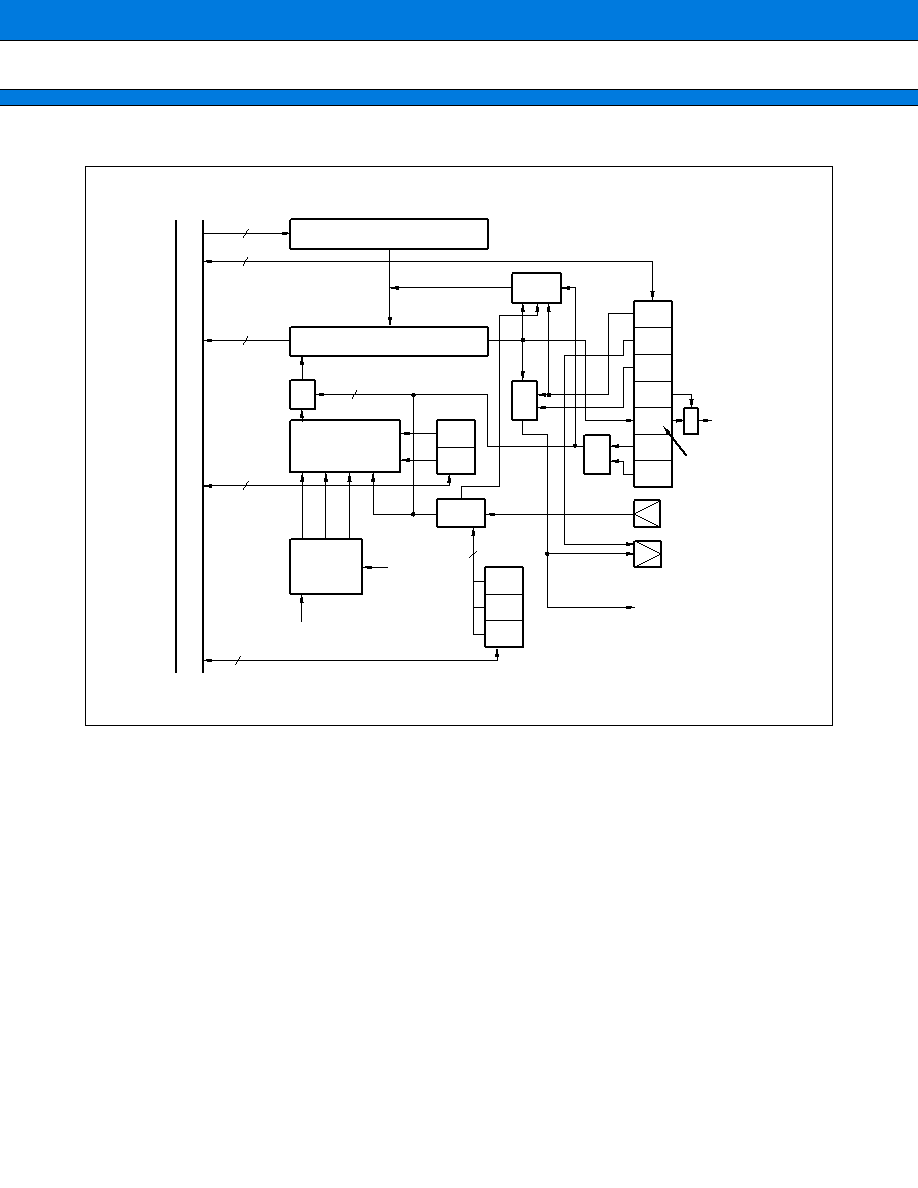
BLOCK DIAGRAM
Clock
control circuit
RAM
Interrupt controller
8
8
8
8
6
8
7
7
P10
to
P17
P20
to
P27
P30
to
P37
P40
to
P47
P50
to
P55
P60
to
P67
P70
to
P76
P80
to
P86
I/O ports
CPU
F
2
MC-16L family core
External interrupts
6
P90
to
P95
8
8
IRT0 to IRT7
7
PA1
to
PA7
X0, 1
RST
HST
MD0 to MD2
Reload timer
Chip select outputs
CS0 to CS7
TIT0, TIT1
TOT0, TOT1
8/16-bit PPG
UART
A/D converter
(8/10-bit)
External bus
Interface
AVcc
AVRH, AVRL
AVss
ATG
AN0 to AN7
SIN0 to SIN2
SOT0 to SOT2
SCK0 to SCK2
Communication prescaler
PPG0
PPG1
A00 to A23
D00 to D15
ALE
RD
WRL, WRH
HRQ
HAK
RDY
CLK
F
2
MC-16 bus
(output switching)
◊
1channel
7
3
3
3
16
2
2
2
2
8
24
MB90610A Series
16
s
s
s
s
F
2
MC-16L CPU PROGRAMMING MODEL
AH
AL
DPR
PCB
DTB
USB
SSB
ADB
8 bits
16 bits
32 bits
Accumulator
USP
SSP
PS
PC
User stack pointer
System stack pointer
Processor status
Program counter
Direct page register
Program bank register
Data bank register
User stack bank register
System stack bank register
Additional data bank register
32 banks (max.)
R7
R6
R5
R4
R3
R2
R1
R0
RW3
RW2
RW1
RW0
16 bits
000180
H
+ RP
◊
10
H
RW7
RW6
RW5
RW4
RL3
RL2
RL1
RL0
ILM
RP
I
S
T
N
Z
V
C
CCR
∑ Dedicated Registers
∑ Processor States (PS)
∑ General-purpose Registers
MB90610A Series
17
s
s
s
s
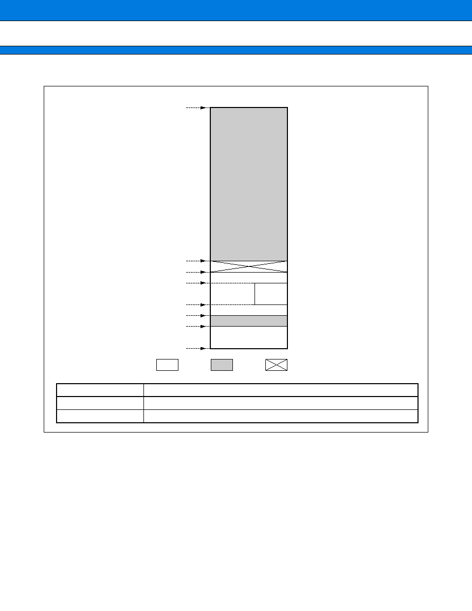
MEMORY MAP
FFFFFF
H
000380
H
002000
H
Address 3#
000180
H
000100
H
0000C0
H
000000
H
External ROM/External bus
RAM
Registers
Peripherals
: Internal
: External
: No access
Type
Address #3
MB90611A
000500
H
MB90613A
000D00
H
MB90610A Series
18
s
s
s
s
I/O MAP
(Continued)
Address
Register
Name
Access
Resource name
Initial value
000000
H
Free
--
*3
--
--
000001
H
Port 1 data register
PDR1
R/W*
Port 1
*8
XXXXXXXX
000002
H
Port 2 data register
PDR2
R/W*
Port 2
*7
XXXXXXXX
000003
H
Port 3 data register
PDR3
R/W*
Port 3
*7
XXXXXXXX
000004
H
Port 4 data register
PDR4
R/W
Port 4
XXXXXXXX
000005
H
Port 5 data register
PDR5
R/W
Port 5
≠≠XXXXXX
000006
H
Port 6 data register
PDR6
R/W
Port 6
11111111
000007
H
Port 7 data register
PDR7
R/W
Port 7
≠XXXXXXX
000008
H
Port 8 data register
PDR8
R/W
Port 8
≠XXXXXXX
000009
H
Port 9 data register
PDR9
R/W
Port 9
≠≠XXXXXX
00000A
H
Port A data register
PDRA
R/W
Port A
XXXXXXX≠
00000B
H
to 10
H
Vacancy
--
*3
--
--
000011
H
Port 1 direction register
DDR1
R/W*
Port 1
*8
00000000
000012
H
Port 2 direction register
DDR2
R/W*
Port 2
*7
00000000
000013
H
Port 3 direction register
DDR3
R/W*
Port 3
*7
00000000
000014
H
Port 4 direction register
DDR4
R/W
Port 4
00000000
000015
H
Port 5 direction register
DDR5
R/W
Port 5
≠≠000000
000016
H
Analog input enable register
ADER
R/W
Port 6
11111111
000017
H
Port 7 direction register
DDR7
R/W
Port 7
≠0000000
000018
H
Port 8 direction register
DDR8
R/W
Port 8
≠0000000
000019
H
Port 9 direction register
DDR9
R/W
Port 9
≠≠000000
00001A
H
Port A direction register
DDRA
R/W
Port A
0000000≠
00001B
H
to 1F
H
Vacancy
--
*3
--
--
000020
H
Serial mode register 0
SMR0
R/W!
UART0 (SCI)
00000000
000021
H
Serial control register 0
SCR0
R/W!
00000100
000022
H
Serial input data register 0/
Serial output data register 0
SIDR0/
SODR0
R/W
XXXXXXXX
000023
H
Serial status register 0
SSR0
R/W!
00001≠00
000024
H
Serial mode register 1
SMR1
R/W!
UART1 (SCI)
00000000
000025
H
Serial control register 1
SCR1
R/W!
00000100
000026
H
Serial input data register 1/
Serial output data register 1
SIDR1/
SODR1
R/W
XXXXXXXX
000027
H
Serial status register 1
SSR1
R/W!
00001≠00
MB90610A Series
19
(Continued)
Address
Register
Name
Access
Resource name
Initial value
000028
H
Interrupt/DTP enable register
ENIR
R/W
DTP/external in-
terrupt
00000000
000029
H
Interrupt/DTP
request
register
EIRR
R/W
00000000
00002A
H
Interrupt level setting register
ELVR
R/W
00000000
00002B
H
00000000
00002C
H
AD control status register
ADCS
R/W!
A/D converter
00000000
00002D
H
00000000
00002E
H
AD data register
ADCR
R/W!
*4
XXXXXXXX
00002F
H
000000XX
000030
H
PPG0 operation mode control regis-
ter
PPGC0
R/W
PPG0
000000≠1
000031
H
PPG1 operation mode control regis-
ter
PPGC1
R/W
PPG1
000000≠1
000032
H
,
33
H
Vacancy
--
*3
--
--
000034
H
PPG0 reload register
PRL0
R/W
PPG0
XXXXXXXX
000035
H
XXXXXXXX
000036
H
PPG1 reload register
PRL1
R/W
PPG1
XXXXXXXX
000037
H
XXXXXXXX
000038
H
Control status register
TMCSR0
R/W!
16-bit reload tim-
er 0
00000000
000039
H
≠≠≠≠0000
00003A
H
16-bit timer register/
16-bit reload register
TMR0/
TMRLR0
R/W
XXXXXXXX
00003B
H
XXXXXXXX
00003C
H
Control status register
TMCSR1
R/W!
16-bit reload tim-
er 1
00000000
00003D
H
≠≠≠≠0000
00003E
H
16-bit timer register/
16-bit reload register
TMR1/
TMRLR1
R/W
XXXXXXXX
00003F
H
XXXXXXXX
000040
H
to 43
H
Vacancy
--
*3
--
--
000044
H
Serial mode register 2
SMR2
R/W!
UART2 (SCI)
00000000
000045
H
Serial control register 2
SCR2
R/W!
00000100
000046
H
Serial input data register 2/
Serial output data register 2
SIDR2/
SODR2
R/W
XXXXXXXX
000047
H
Serial status register 2
SSR2
R/W!
00001≠00
000048
H
CS control register 0
CSCR0
R/W
Chip select func-
tion
≠≠≠≠0000
000049
H
CS control register 1
CSCR1
R/W
≠≠≠≠0000
00004A
H
CS control register 2
CSCR2
R/W
≠≠≠≠0000
00004B
H
CS control register 3
CSCR3
R/W
≠≠≠≠0000
MB90610A Series
20
(Continued)
Address
Register
Name
Access
*2
Resource name
Initial value
00004C
H
CS control register 4
CSCR4
R/W
Chip select
function
≠≠≠≠0000
00004D
H
CS control register 5
CSCR5
R/W
≠≠≠≠0000
00004E
H
CS control register 6
CSCR6
R/W
≠≠≠≠0000
00004F
H
CS control register 7
CSCR7
R/W
≠≠≠≠0000
000050
H
Vacancy
--
*3
--
--
000051
H
UART0 (SCI) machine clock division
control register
CDCR0
W
UART0 (SCI)
≠≠≠≠1111
000052
H
Vacancy
--
*3
--
--
000053
H
UART1 (SCI) machine clock division
control register
CDCR1
W
UART1 (SCI)
≠≠≠≠1111
000054
H
Vacancy
--
*3
--
--
000055
H
UART2 (SCI) machine clock division
control register
CDCR2
W
UART2 (SCI)
≠≠≠≠1111
000056
H
to 8F
H
Vacancy
--
*3
--
--
000090
H
to 9E
H
Reserved system area
--
*1
--
--
00009F
H
Delayed interrupt generate/
release register
DIRR
R/W
Delayed interrupt
generation
module
≠≠≠≠≠≠≠0
0000A0
H
Low power consumption mode con-
trol register
LPMCR
R/W!
Low power
consumption
00011000
0000A1
H
Clock selection register
CKSCR
R/W!
Low power con-
sumption
11111100
0000A2
H
to A4
H
Vacancy
--
*3
--
--
0000A5
H
Auto-ready function selection register ARSR
W
External pins
0011≠≠00
0000A6
H
External address output control regis-
ter
HACR
W
External pins
00000000
0000A7
H
Bus control signal selection register
ECSR
W
External pins
≠000*000
0000A8
H
Watchdog timer control register
WDTC
R/W!
Watchdog timer
XXXXX111
0000A9
H
Timebase timer control register
TBTC
R/W!
Timebase timer
1≠≠00100
0000AA
H
to AF
H
Vacancy
--
*3
--
--
0000B0
H
Interrupt control register 00
ICR00
R/W!
Interrupt
controller
00000111
0000B1
H
Interrupt control register 01
ICR01
R/W!
00000111
0000B2
H
Interrupt control register 02
ICR02
R/W!
00000111
0000B3
H
Interrupt control register 03
ICR03
R/W!
00000111
0000B4
H
Interrupt control register 04
ICR04
R/W!
00000111
0000B5
H
Interrupt control register 05
ICR05
R/W!
00000111
MB90610A Series
21
(Continued)
Initial values
0 :The initial value for this bit is "0".
1 :The initial value for this bit is "1".
*
:The initial value for this bit is "1" or "0". (Determined by the level of the MD0 to MD2 pins.)
X :The initial value for this bit is undefined.
≠ :This bit is not used. The initial value is undefined.
*1: Access prohibited.
*2: This is the only external access area in the area below address 0000FF
H
. Access this address as an external
I/O area.
*3: Areas marked as "free" in the I/O map are reserved areas. These areas are accessed by internal access. No
access signals are output on the external bus.
*4: Only bit 15 can be written. The other bits are written to by the test function. Reading bits 10 to 15 returns zeros.
*5: The R/W! symbol in the Read/Write column indicates that some bits are read-only or write-only. See the resource's
register list for details.
*6: Using a read-modify-write instruction (such as the bit set instruction) to access one of the registers indicated
by R/W!, R/W*, or W in the Read/Write column sets the specified bit to the desired value. However, this can
cause misoperation if the other register bits include write-only bits. Therefore, do not use read-modify-write
instructions to access these registers.
*7: This register is only available when the address/data bus is in multiplex mode. Access to the register is prohibited
in non-multiplex mode.
*8: This register is only available when the external data bus is in 8-bit mode. Access to the register is prohibited
in 16-bit mode.
Note: The initial values listed for write-only bits are the initial values set by a reset. They are not the values returned
by a read.
Also, LPMCR/CKSCR/WDTC are sometimes initialized and sometimes not initialized, depending on the
reset type. The listed initial values are for when these registers are initialized.
Address
Register
Name
Access
Resource name
Initial value
0000B6
H
Interrupt control register 06
ICR06
R/W!
Interrupt
controller
00000111
0000B7
H
Interrupt control register 07
ICR07
R/W!
00000111
0000B8
H
Interrupt control register 08
ICR08
R/W!
00000111
0000B9
H
Interrupt control register 09
ICR09
R/W!
00000111
0000BA
H
Interrupt control register 10
ICR10
R/W!
00000111
0000BB
H
Interrupt control register 11
ICR11
R/W!
00000111
0000BC
H
Interrupt control register 12
ICR12
R/W!
00000111
0000BD
H
Interrupt control register 13
ICR13
R/W!
00000111
0000BE
H
Interrupt control register 14
ICR14
R/W!
00000111
0000BF
H
Interrupt control register 15
ICR15
R/W!
00000111
0000C0
H
to FF
H
External area
*2
--
--
--
--
MB90610A Series
22
s
s
s
s
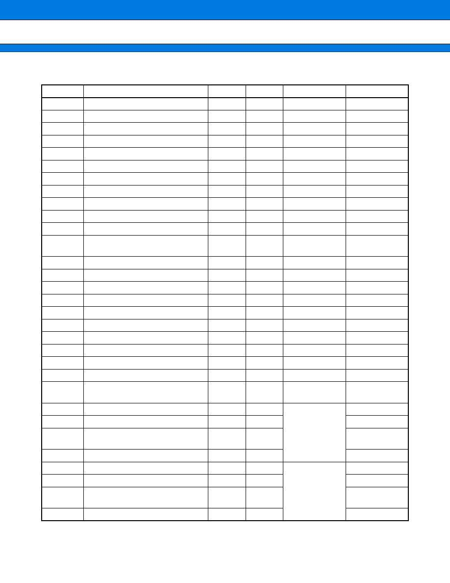
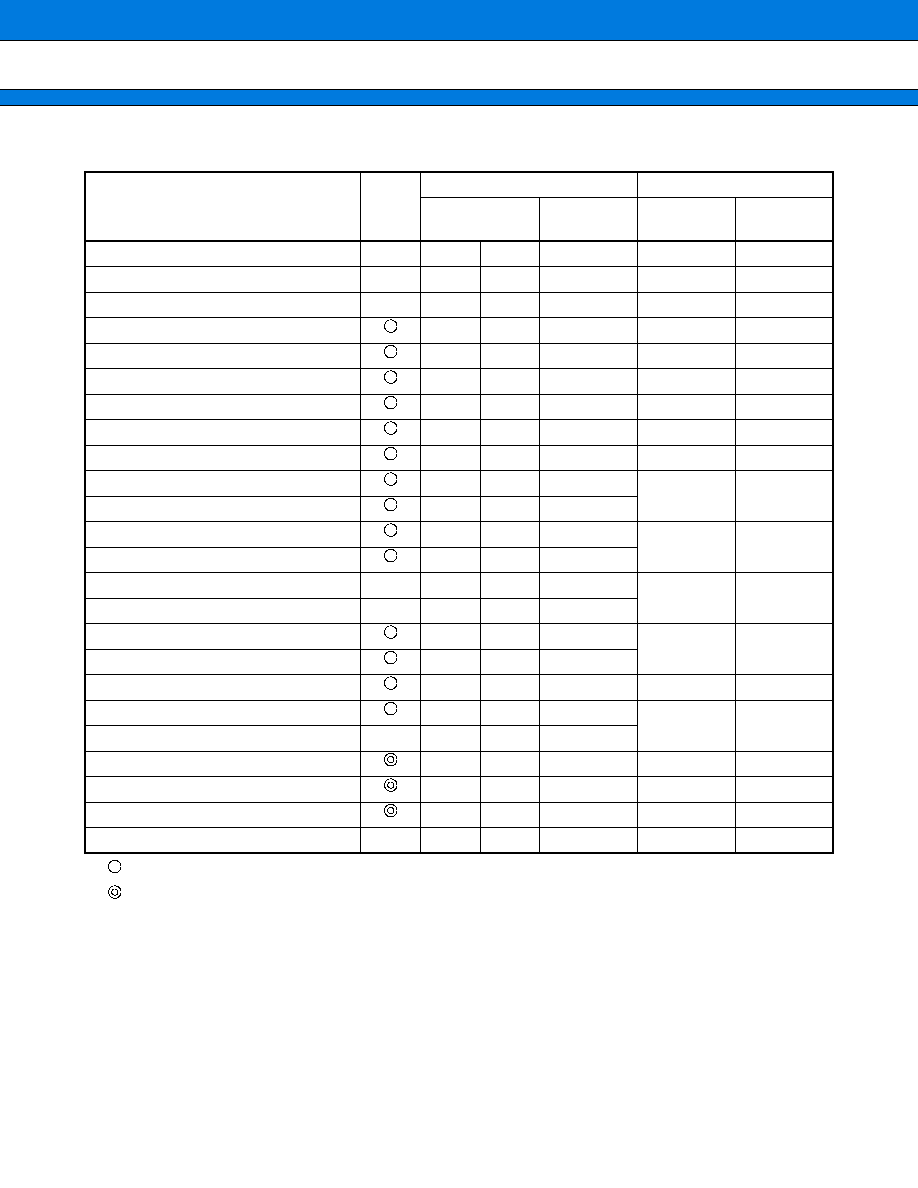
INTERRUPT SOURCE, INTERRUPT VECTORS, AND INTERRUPT CONTROL REGISTER
:indicates that the interrupt request flag is cleared by the I
2
OS interrupt clear signal (no stop request).
:indicates that the interrupt request flag is cleared by the I
2
OS interrupt clear signal (with stop request).
◊
:indicates that the interrupt request flag is not cleared by the I
2
OS interrupt clear signal.
Note: Do not specify I
2
OS activation in interrupt control registers that do not support I
2
OS.
Interrupt source
I
2
OS
sup-
port
Interrupt vector
Interrupt control register
Number
Address
ICR
Address
Reset
◊
#08
08
H
FFFFDC
H
--
--
INT 9 instruction
◊
#09
09
H
FFFFD8
H
--
--
Exception
◊
#10
0A
H
FFFFD4
H
--
--
External interrupt #0
#11
0B
H
FFFFD0
H
ICR00
0000B0
H
External interrupt #1
#13
0D
H
FFFFC8
H
ICR01
0000B1
H
External interrupt #2
#15
0F
H
FFFFC0
H
ICR02
0000B2
H
External interrupt #3
#17
11
H
FFFFB8
H
ICR03
0000B3
H
External interrupt #4
#19
13
H
FFFFB0
H
ICR04
0000B4
H
External interrupt #5
#21
15
H
FFFFA8
H
ICR05
0000B5
H
External interrupt #6
#23
17
H
FFFFA0
H
ICR06
0000B6
H
UART0 ∑ transmit complete
#24
18
H
FFFF9C
H
External interrupt #7
#25
19
H
FFFF98
H
ICR07
0000B7
H
UART1 ∑ transmit complete
#26
1A
H
FFFF94
H
PPG #0
◊
#27
1B
H
FFFF90
H
ICR08
0000B8
H
PPG #1
◊
#28
1C
H
FFFF8C
H
16-bit reload timer #0
#29
1D
H
FFFF88
H
ICR09
0000B9
H
16-bit reload timer #1
#30
1E
H
FFFF84
H
A/DC measurement complete
#31
1F
H
FFFF80
H
ICR10
0000BA
H
UART2 ∑ transmit complete
#33
21
H
FFFF78
H
ICR11
0000BB
H
Timebase timer interval interrupt
◊
#34
22
H
FFFF74
H
UART2 ∑ receive complete
#35
23
H
FFFF70
H
ICR12
0000BC
H
UART1 ∑ receive complete
#37
25
H
FFFF68
H
ICR13
0000BD
H
UART0 ∑ receive complete
#39
27
H
FFFF60
H
ICR14
0000BE
H
Delayed interrupt generation module
◊
#42
2A
H
FFFF54
H
ICR15
0000BF
H
MB90610A Series
23
s
s
s
s
PERIPHERAL RESOURCES
1.
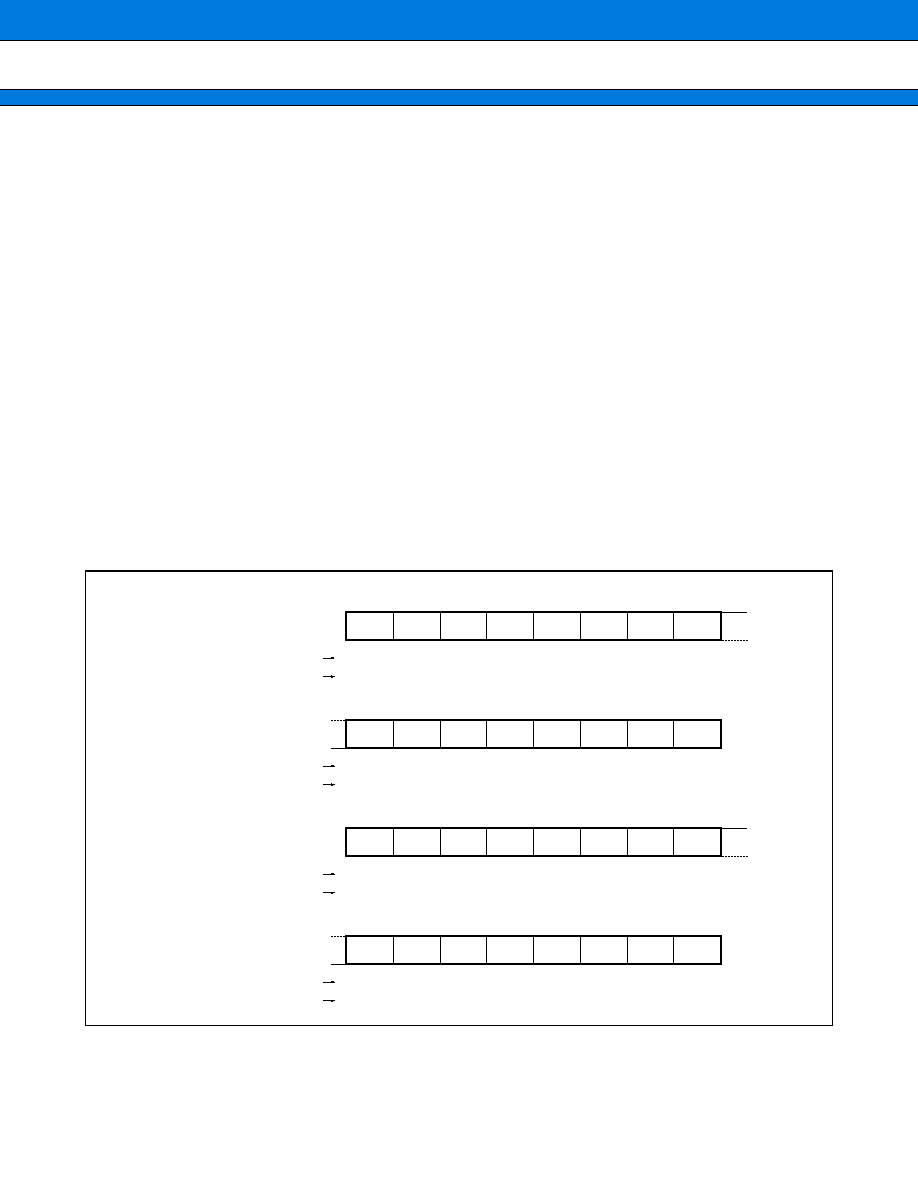
Parallel Port
The MB90610A series has 58 I/O pins, 18 output pins, and 8 open drain output pins.
Ports 1 to 5 and ports 7 to A are I/O ports. The ports are inputs when the corresponding direction register bit is
"0" and outputs when the corresponding bit is "1".
Port 1 is only available when the external data bus is in 8-bit mode. Access is prohibited in 16-bit mode.
Ports 2 and 3 are only available when the address/data bus is in multiplex mode. Access is prohibited in non-
multiplex mode.
Port 6 is an open drain port. Port 6 pins can only be used as ports when the analog input enable register is "0".
(1) Register Configuration
bit
Read/write
Initial value
bit
PD
◊
7 PD
◊
6 PD
◊
5 PD
◊
4 PD
◊
3 PD
◊
2 PD
◊
1 PD
◊
0
PDR
◊
(R/W)
(X)
(R/W)
(X)
(R/W)
(X)
(R/W)
(X)
(R/W)
(X)
(R/W)
(X)
(R/W)
(X)
(R/W)
(X)
15
14
13
12
11
10
9
8
PD
◊
7 PD
◊
6 PD
◊
5 PD
◊
4 PD
◊
3 PD
◊
2 PD
◊
1 PD
◊
0
PDR
◊
(R/W)
(X)
(R/W)
(X)
(R/W)
(X)
(R/W)
(X)
(R/W)
(X)
(R/W)
(X)
(R/W)
(X)
(R/W)
(X)
7
6
5
4
3
2
1
0
Read/write
Initial value
Port data register
Address : PDR1 000001
H
: PDR3 000003
H
: PDR5 000005
H
: PDR7 000007
H
: PDR9 000009
H
Port data register
Address : PDR2 000002
H
: PDR4 000004
H
: PDR6 000006
H
: PDR8 000008
H
: PDRA 00000A
H
Notes: No register bits are provided for bit 6 to 7 of port 5.
No register bit is provided for bit 7 of port 7.
No register bit is provided for bit 7 of port 8.
No register bits are provided for bits 6 to 7 of port 9.
No register bit is provided for bit 0 of port A.
MB90610A Series
24
bit
Read/write
Initial value
bit
DD
◊
7 DD
◊
6 DD
◊
5 DD
◊
4 DD
◊
3 DD
◊
2 DD
◊
1 DD
◊
0
DDR
◊
(R/W)
(0)
(R/W)
(0)
(R/W)
(0)
(R/W)
(0)
(R/W)
(0)
(R/W)
(0)
(R/W)
(0)
(R/W)
(0)
15
14
13
12
11
10
9
8
DD
◊
7 DD
◊
6 DD
◊
5 DD
◊
4 DD
◊
3 DD
◊
2 DD
◊
1 DD
◊
0
DDR
◊
(R/W)
(0)
(R/W)
(0)
(R/W)
(0)
(R/W)
(0)
(R/W)
(0)
(R/W)
(0)
(R/W)
(0)
(R/W)
(0)
7
6
5
4
3
2
1
0
Read/write
Initial value
Port direction register
Address : DDR1 000011
H
: DDR3 000013
H
: DDR5 000015
H
: DDR7 000017
H
: DDR9 000019
H
Port direction register
Address : DDR2 000012
H
: DDR4 000014
H
: DDR8 000018
H
: DDRA 00001A
H
Note: No register bits are provided for bit 6 to 7 of port 5.
No register bit is provided for bit 7 of port 7.
No register bit is provided for bit 7 of port 8.
No register bits are provided for bits 6 to 7 of port 9.
No register bit is provided for bit 0 of port A.
Port 6 does not have a DDR.
bit
Read/write
Initial value
ADE7 ADE6 ADE5 ADE4 ADE3 ADE2 ADE1 ADE0
ADER
(R/W)
(1)
(R/W)
(1)
(R/W)
(1)
(R/W)
(1)
(R/W)
(1)
(R/W)
(1)
(R/W)
(1)
(R/W)
(1)
15
14
13
12
11
10
9
8
Analog input enable register
ADER 000016
H
MB90610A Series
25
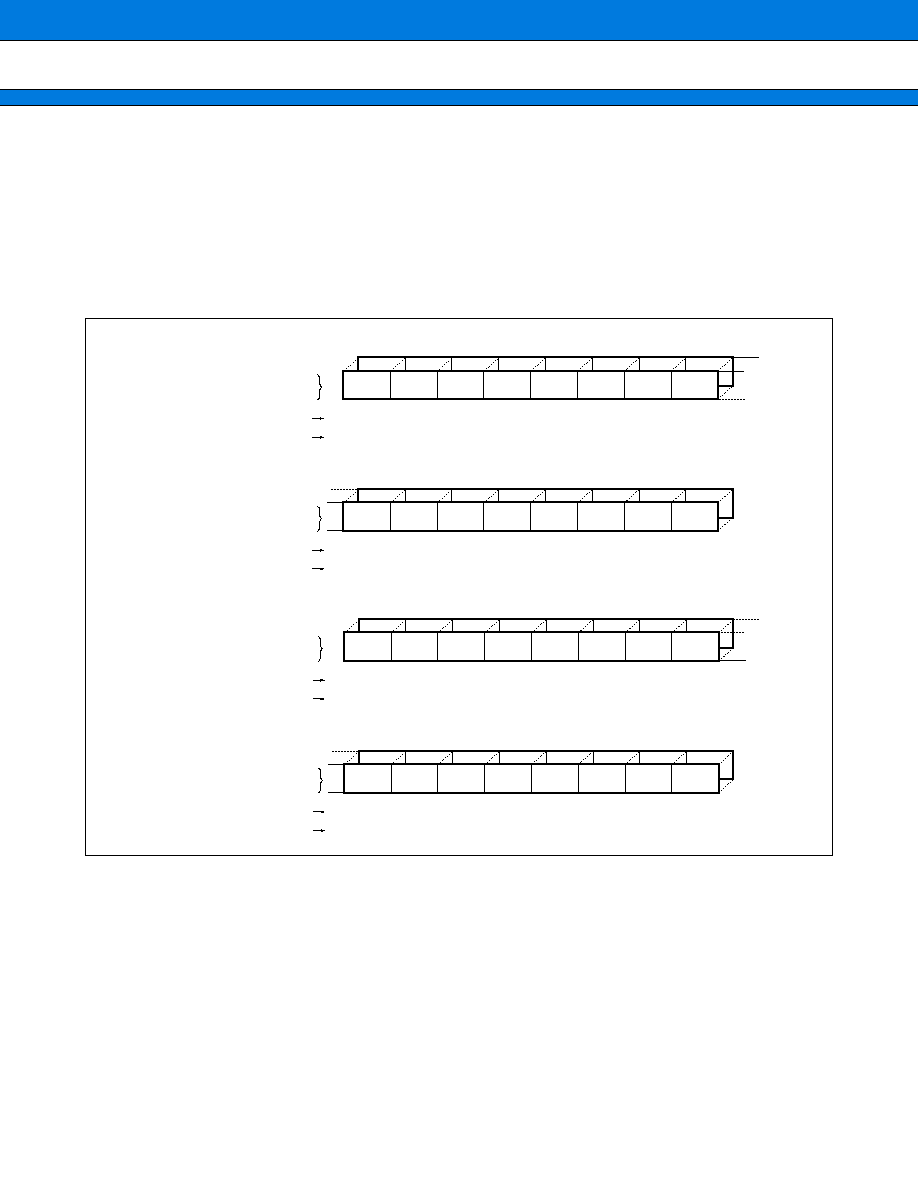
(2) Register Details
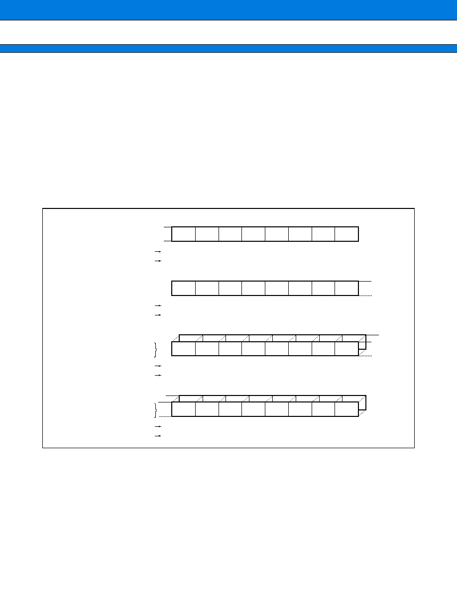
∑ Port Data Registers
bit
Read/write
Initial value
bit
PD
◊
7 PD
◊
6 PD
◊
5 PD
◊
4 PD
◊
3 PD
◊
2 PD
◊
1 PD
◊
0
PDR
◊
(R/W)
(X)
(R/W)
(X)
(R/W)
(X)
(R/W)
(X)
(R/W)
(X)
(R/W)
(X)
(R/W)
(X)
(R/W)
(X)
15
14
13
12
11
10
9
8
PD
◊
7 PD
◊
6 PD
◊
5 PD
◊
4 PD
◊
3 PD
◊
2 PD
◊
1 PD
◊
0
PDR
◊
(R/W)
(X)
(R/W)
(X)
(R/W)
(X)
(R/W)
(X)
(R/W)
(X)
(R/W)
(X)
(R/W)
(X)
(R/W)
(X)
7
6
5
4
3
2
1
0
Read/write
Initial value
Port data register
Address : PDR1 000001
H
: PDR3 000003
H
: PDR5 000005
H
: PDR7 000007
H
: PDR9 000009
H
Port data register
Address : PDR2 000002
H
: PDR4 000004
H
: PDR6 000006
H
: PDR8 000008
H
: PDRA 00000A
H
Note: No register bits are provided for bit 6 to 7 of port 5.
No register bit is provided for bit 7 of port 7.
No register bit is provided for bit 7 of port 8.
No register bits are provided for bits 6 to 7 of port 9.
No register bit is provided for bit 0 of port A.
Port 1 is only available when the external data bus is in 8-bit mode. Access is prohibited in 16-bit mode.
Ports 2, 3 are only available in multiplex mode. Access is prohibited in non-multiplex mode.
MB90610A Series
26
∑ Port Direction Registers
∑ Analog Input Enable Register
bit
Read/write
Initial value
bit
DD
◊
7 DD
◊
6 DD
◊
5 DD
◊
4 DD
◊
3 DD
◊
2 DD
◊
1 DD
◊
0
DDR
◊
(R/W)
(0)
(R/W)
(0)
(R/W)
(0)
(R/W)
(0)
(R/W)
(0)
(R/W)
(0)
(R/W)
(0)
(R/W)
(0)
15
14
13
12
11
10
9
8
DD
◊
7 DD
◊
6 DD
◊
5 DD
◊
4 DD
◊
3 DD
◊
2 DD
◊
1 DD
◊
0
DDR
◊
(R/W)
(0)
(R/W)
(0)
(R/W)
(0)
(R/W)
(0)
(R/W)
(0)
(R/W)
(0)
(R/W)
(0)
(R/W)
(0)
7
6
5
4
3
2
1
0
Read/write
Initial value
Port direction register
Address : DDR1 000011
H
: DDR3 000013
H
: DDR5 000015
H
: DDR7 000017
H
: DDR9 000019
H
Port direction register
Address : DDR2 000012
H
: DDR4 000014
H
: DDR8 000018
H
: DDRA 00001A
H
When pins are used as ports, the register bits control the corresponding pins as follows.
0: Input mode
1: Output mode
Bits are set to "0" by a reset.
Note: No register bits are provided for bit 6 to 7 of port 5.
No register bit is provided for bit 7 of port 7.
No register bit is provided for bit 7 of port 8.
No register bit is provided for bit 0 of port A.
No register bits are provided for bits 6 to 7 of port 9.
Port 6 does not have a DDR.
Port 1 is only available when the external data bus is in 8-bit mode. Access is prohibited in 16-bit mode.
Ports 2 and 3 are only available in multiplex mode. Access is prohibited in non-multiplex mode.
bit
Read/write
Initial value
ADE7 ADE6 ADE5 ADE4 ADE3 ADE2 ADE1 ADE0
ADER
(R/W)
(1)
(R/W)
(1)
(R/W)
(1)
(R/W)
(1)
(R/W)
(1)
(R/W)
(1)
(R/W)
(1)
(R/W)
(1)
15
14
13
12
11
10
9
8
Analog input enable register
ADER 000016
H
Controls each pin of port 6 as follows.
0: Port input mode
1: Analog input mode
Bits are set to "1" by a reset.
Note: Inputting an intermediate level signal in port input mode causes an input leak current to flow. Therefore,
set to analog input mode when applying an analog input.
MB90610A Series
27
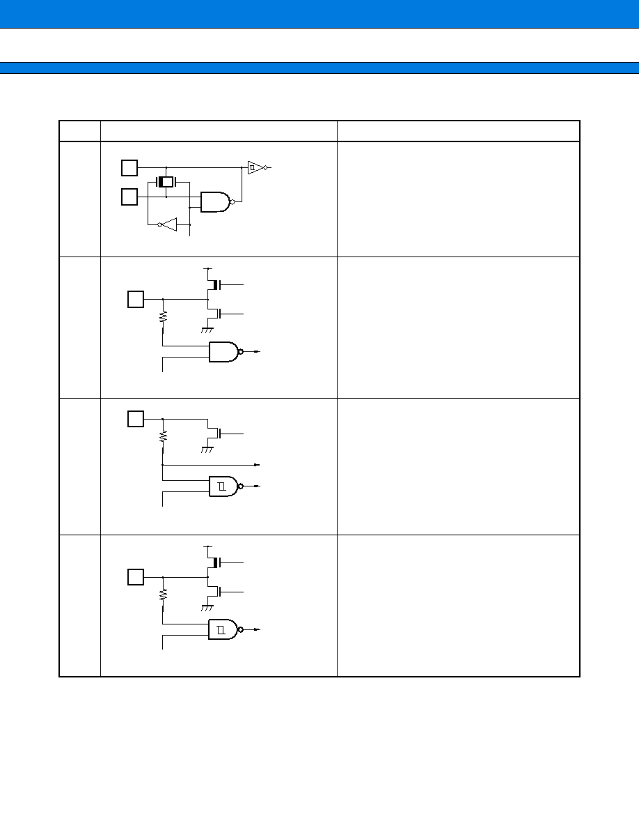
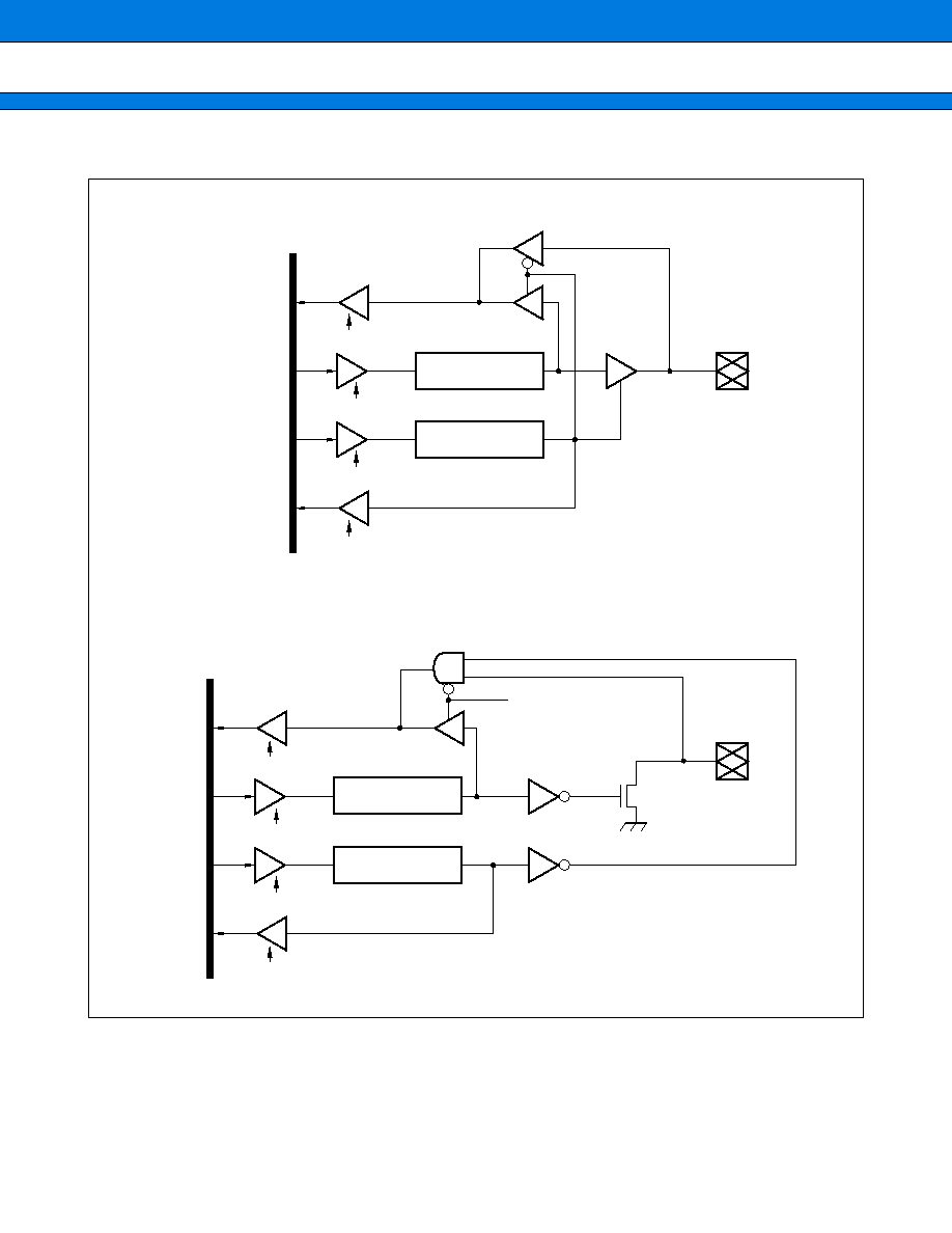
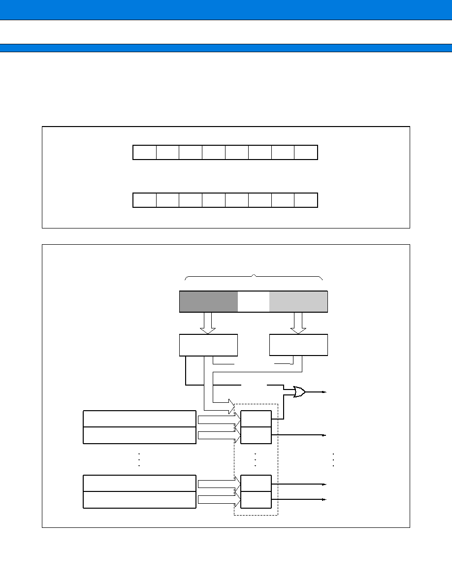
(3) Block Diagrams
Internal data bus
Data register
Direction register
Data register read
Data register write
Direction register write
Direction register read
Pin
Internal data bus
Data register
ADER
Data register read
Data register write
ADER register write
ADER register read
Pin
RMW
(Read-modify-write instruction)
∑ I/O Port
∑ Open Drain Port (Also used as Analog Inputs)
MB90610A Series
28
(4) Port Pin Allocation
Ports 1, 2, 3, 4, and 5 on the MB90610A series share pins with the external bus. The pin functions are determined
by the bus mode and register settings.
Note: The upper address, WRL, WRH, HAK, HRQ, RDY, and CLK can be set for use as ports by function selection.
Pin
Function
Non-multiplex mode
Multiplex mode
External address control
External address control
Enable (address)
Disable (port)
Enable (address)
Disable (port)
External bus width
External bus width
External bus width
External bus width
8-bit
16-bit
8-bit
16-bit
8-bit
16-bit
8-bit
16-bit
D07 to D00
AD07 to
AD00
D07 to D00
AD07 to AD00
P17 to P10/
D15 to D08/
AD15 to
AD08
Port
D15 to D08
Port
D15 to D08 A15 to A08
AD15 to
AD08
A15 to A08
AD15 to
AD08
P27 to P20/
A07 to A00
A07 to A00
A07 to A00
Port
P37 to P30/
A15 to A08
A15 to A08
A15 to A08
P47 to P40/
A23 to A16
A23 to A16
Port
A23 to A16
Port
P57/ALE
ALE
ALE
RD
RD
RD
P55/WRL
WRL
WRL
P54/WRH
Port
WRH
Port
WRH
Port
WRH
Port
WRH
P53/HRQ
HRQ
HRQ
P52/HAK
HAK
HAK
P51/RDY
RDY
RDY
P50/CLK
CLK
CLK
MB90610A Series
29
2.
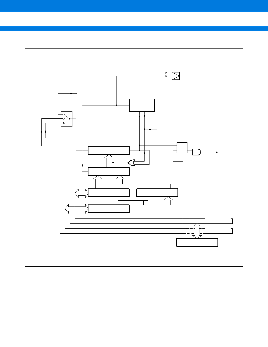
UART 0/1/2 (SCI)
UART 0/1/2 are serial I/O ports that can be used for CLK asynchronous (start-stop synchronization) or CLK
synchronous (I/O expansion serial) data transfer. The ports have the following features.
∑ Full duplex, double buffered
∑ Supports CLK asynchronous (start-stop synchronization) and CLK synchronous (I/O expansion serial) data
transfer
∑ Multi-processor mode support
∑ Built-in dedicated baud rate generator
CLK asynchronous: 62500/31250/19230/9615/4808/2404/1202 bps
CLK synchronous: 2 M/1 M/500 K/250 K bps
∑ Supports flexible baud rate setting using an external clock
∑ Error detect function (parity, framing, and overrun)
∑ NRZ type transmission signal
∑ Intelligent I/O service support
(1) Register Configuration
bit
Read/write
Initial value
bit
PEN
P
SBL
CL
A/D
REC
RXE
TXE
SCR
(R/W)
(0)
(R/W)
(0)
(R/W)
(0)
(R/W)
(0)
(R/W)
(0)
(R/W)
(1)
(R/W)
(0)
(R/W)
(0)
15
14
13
12
11
10
9
8
MD1
MD0
CS2
CS1
CS0
≠
SCKE SOE
SMR
(R/W)
(0)
(R/W)
(0)
(W)
(0)
(W)
(0)
(W)
(0)
(≠)
(≠)
(R/W)
(0)
(R/W)
(0)
7
6
5
4
3
2
1
0
Read/write
Initial value
Serial control register
Address : channel 0 000021
H
: channel 1 000025
H
: channel 2 000045
H
Serial mode register
Address : channel 0 000020
H
: channel 1 000024
H
: channel 2 000044
H
bit
Read/write
Initial value
bit
PE
ORE
FRE RDRF TDRE
≠
RIE
TIE
SSR
(R)
(0)
(R)
(0)
(R)
(0)
(R)
(0)
(R)
(1)
(≠)
(≠)
(R/W)
(0)
(R/W)
(0)
15
14
13
12
11
10
9
8
D7
D6
D5
D4
D3
D2
D1
D0
SIDR (read)
SODR (write)
(R/W)
(X)
(R/W)
(X)
(R/W)
(X)
(R/W)
(X)
(R/W)
(X)
(R/W)
(X)
(R/W)
(X)
(R/W)
(X)
7
6
5
4
3
2
1
0
Read/write
Initial value
Serial status register
Address : channel 0 000023
H
: channel 1 000027
H
: channel 2 000047
H
bit
Read/write
Initial value
≠
≠
≠
≠
DIV3 DIV1 DIV1 DIV0
CDCR
(≠)
(≠)
(≠)
(≠)
(≠)
(≠)
(≠)
(≠)
(W)
(1)
(W)
(1)
(W)
(1)
(W)
(1)
15
14
13
12
11
10
9
8
Machine clock division
control register
Address : channel 0 000051
H
: channel 1 000053
H
: channel 2 000055
H
Input data register/
Output data register
Address : channel 0 000022
H
: channel 1 000026
H
: channel 2 000046
H
MB90610A Series
30
(2) Block Diagram
Control signals
Dedicated baud
rate generator
16-bit timer 0
(Internal connection)
External clock
SIN
Clock select
circuit
Receive interrupt
(to CPU)
Transmit interrupt
(to CPU)
Receive control circuit
Start bit
detect circuit
Receive bit counter
Receive parity
counter
Transmit control circuit
Transmit start circuit
Transmit bit counter
Transmit parity
counter
Receive status
evaluation circuit
Receive shifter
Receive
complete
Transmit shifter
Transmit
start
Receive error
indication signal
for EI
2
OS (to CPU)
SIDR
SODR
F
2
MC-16 bus
SMR
register
MD1
MD0
CS2
CS1
CS0
SCKE
SOE
SCR
register
SSR
register
Control signals
Transmit clock
Receive clock
SOT
PEN
P
SBL
CL
A/D
REC
RXE
TXE
PE
ORE
FRE
RDRF
TDRE
RIE
TIE
SCK
MB90610A Series
31
3.
10-bit 8-input A/D Converter (With 8-bit Resolution Mode)
The 10-bit 8-input A/D converter converts analog input voltages to digital values. The A/D converter has the
following features.
∑ Conversion time: Minimum of 6.13
µ
s per channel (98 machine cycles/16 MHz machine clock. This includes
the sample and hold time)
∑ Sample and hold time: Minimum of 3.75
µ
s per channel (60 machine cycles/16 MHz machine clock)
∑ Uses RC-type successive approximation conversion with a sample and hold circuit.
∑ 10-bit or 8-bit resolution
∑ Eight program-selectable analog input channels
Single conversion mode
: Selectively convert a one channel.
Scan conversion mode
: Continuously convert multiple channels. Maximum of 8 program-selectable
channels.
Continuous conversion mode
: Repeatedly convert specified channels.
Stop conversion mode
: Convert one channel then halt until the next activation. (Enables
synchronization of the conversion start timing.)
∑ An A/D conversion completion interrupt request to the CPU can be generated on the completion of A/D
conversion. This interrupt can activate I
2
OS to transfer the result of A/D conversion to memory and is suitable
for continuous operation.
∑ Activation by software, external trigger (falling edge), or timer (rising edge) can be selected.
(1) Register Configuration
bit
Read/write
Initial value
BUSY
INT
INTE PAUS STS1 STS0 STRT
Reserved
ADCS1
(R/W)
(0)
(R/W)
(0)
(R/W)
(0)
(R/W)
(0)
(R/W)
(0)
(R/W)
(0)
(W)
(0)
(≠)
(0)
15
14
13
12
11
10
9
8
A/D control status register (upper)
Address : 00002D
H
bit
Read/write
Initial value
MD1
MD0 ANS2 ANS1 ANS0 ANE2 ANE1 ANE0
ADCS0
(R/W)
(0)
(R/W)
(0)
(R/W)
(0)
(R/W)
(0)
(R/W)
(0)
(R/W)
(0)
(R/W)
(0)
(R/W)
(0)
7
6
5
4
3
2
1
0
A/D control status register (lower)
Address : 00002C
H
bit
Read/write
Initial value
S10
≠
≠
≠
≠
≠
D9
D8
ADCR1
(R/W)
(0)
(R)
(0)
(R)
(0)
(R)
(0)
(R)
(0)
(R)
(0)
(R)
(X)
(R)
(X)
15
14
13
12
11
10
9
8
A/D data register (upper)
Address : 00002E
H
bit
Read/write
Initial value
D7
D6
D5
D4
D3
D2
D1
D0
ADCR0
(R)
(X)
(R)
(X)
(R)
(X)
(R)
(X)
(R)
(X)
(R)
(X)
(R)
(X)
(R)
(X)
7
6
5
4
3
2
1
0
A/D data register (lower)
Address : 00002F
H
MB90610A Series
32
(2) Block Diagram
AV
CC
AVRH
AVRL
AN0
AN1
AN2
AN3
AN4
AN5
AN6
AN7
MPX
Sample and hold circuit
Comparator
D/A converter
Successive
approximation register
Data register
A/D control register 1
A/D control register 2
ADCR
ADCS
ATG
Timer
(Reload timer 1 output)
Timer activation
Trigger activation
Operating clock
Prescaler
AV
SS
Input circuit
Decoder
Data bus
MB90610A Series
33
4.
8/16-bit PPG
This block contains the 8-bit reload timer module. The block performs PPG output in which the pulse output is
controlled by the operation of the timer.
The hardware consists of two 8-bit down-counters, four 8-bit reload registers, one 16-bit control register, two
external pulse output pins, and two interrupt outputs. The PPG has the following functions.
∑ 8-bit PPG output in 2-channel independent operation mode:Two independent PPG output channels are
available.
∑ 16-bit PPG output operation mode:
One 16-bit PPG output channel is available.
∑ 8+8-bit PPG output operation mode: Variable-period 8-bit PPG output operation is available by using the out-
put of channel 0 as the clock input to channel 1.
∑ PPG output operation:Outputs pulse waveforms with variable period and duty ratio.
Can be used as a D/A converter in conjunction with an external circuit.
(1) Register Configuration
bit
Read/write
Initial value
bit
PEN1 PCS1 POE1 PIE1 PUF1 MD1
MD0
Reserved
PPGC1
(R/W)
(0)
(R/W)
(0)
(R/W)
(0)
(R/W)
(0)
(R/W)
(0)
(R/W)
(0)
(R/W)
(0)
(--)
(1)
15
14
13
12
11
10
9
8
PEN0
--
POE0 PIE0 PUF0 PCM1 PCM0
Reserved
PPGC0
(R/W)
(0)
(--)
(0)
(R/W)
(0)
(R/W)
(0)
(R/W)
(0)
(R/W)
(0)
(R/W)
(0)
(--)
(1)
7
6
5
4
3
2
1
0
Read/write
Initial value
PPG1 operation mode
control register
Address : channel 1 000031
H
bit
Read/write
Initial value
PRLH0, 1
(R/W)
(X)
(R/W)
(X)
(R/W)
(X)
(R/W)
(X)
(R/W)
(X)
(R/W)
(X)
(R/W)
(X)
(R/W)
(X)
15
14
13
12
11
10
9
8
Reload register H
Address : channel 0 000035
H
: channel 1 000037
H
bit
Read/write
Initial value
PRLL0, 1
(R/W)
(X)
(R/W)
(X)
(R/W)
(X)
(R/W)
(X)
(R/W)
(X)
(R/W)
(X)
(R/W)
(X)
(R/W)
(X)
7
6
5
4
3
2
1
0
Reload register L
Address : channel 0 000034
H
: channel 1 000036
H
PPG0 operation mode
control register
Address : channel 0 000030
H
MB90610A Series
34
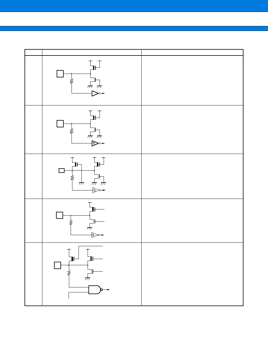
(2) Block Diagram
PPG0
output latch
PCNT (down-counter)
S
R Q
Output enable
L/H selector
PRLBH0
PPGC0
Peripheral clock divided by 16
Peripheral clock divided by 4
Peripheral clock
PRLL0
PRLH0
L-side data bus
H-side data bus
PPG0
Clear
Invert
PEN0
Reload
ch.1 borrow
IRQ
Count clock
selection
Timebase counter output
Main clock divided by 512
L/H select
PIE 0
PUF0
(Operation mode control)
∑ 8/16-bit PPG (channel 0)
MB90610A Series
35
PPG1
output latch
PCNT (down-counter)
S
R Q
Output enable
L/H selector
PRLBH1
PPGC1
Peripheral clock
PRLL1
PRLH1
L-side data bus
H-side data bus
PPG1
Clear
Invert
PEN1
Reload
channel 0 borrow
IRQ
Timebase counter output
Main clock divided by 512
L/H select
PIE1
PUF1
(Operation mode control)
Count clock
selection
∑ 8/16-bit PPG (channel 1)
MB90610A Series
36
5.
16-bit Reload Timer (with Event Count Function)
The 16-bit reload timers consists of a 16-bit down-counter, a 16-bit reload register, one input (TIN) and one
output (TOT) pin, and a control register. The input clock can be selected from one external clock and three types
of internal clock. The output pin (TOT) outputs a toggle waveform in reload mode and a rectangular waveform
during counting in one-shot mode. The input pin (TIN) functions as the event input in event count mode and as
the trigger input or gate input in internal clock mode.
This product has two internal 16-bit reload timer channels.
(1) Register Configuration
Timer control
status register (upper)
Address : channel 0 000039
H
: channel 1 00003D
H
bit
Read/write
Initial value
bit
--
--
--
--
CSL1 CSL2 MOD2 MOD1
(--)
(--)
(--)
(--)
(--)
(--)
(--)
(--)
(R/W)
(0)
(R/W)
(0)
(R/W)
(0)
(R/W)
(0)
15
14
13
12
11
10
9
8
MOD0 OUTE OUTL RELD INTE
UF
CNTE TRG
TMCSR
(R/W)
(0)
(R/W)
(0)
(R/W)
(0)
(R/W)
(0)
(R/W)
(0)
(R/W)
(0)
(R/W)
(0)
(R/W)
(0)
7
6
5
4
3
2
1
0
Read/write
Initial value
Timer control
status register (lower)
Address : channel 0 000038
H
: channel 1 00003C
H
16-bit timer register (upper)/
16-bit reload register (upper)
Address : channel 0 00003B
H
: channel 1 00003F
H
bit
Read/write
Initial value
bit
(R/W)
(X)
(R/W)
(X)
(R/W)
(X)
(R/W)
(X)
(R/W)
(X)
(R/W)
(X)
(R/W)
(X)
(R/W)
(X)
15
14
13
12
11
10
9
8
TMR/
TMRLR
(R/W)
(X)
(R/W)
(X)
(R/W)
(X)
(R/W)
(X)
(R/W)
(X)
(R/W)
(X)
(R/W)
(X)
(R/W)
(X)
7
6
5
4
3
2
1
0
Read/write
Initial value
16-bit timer register (lower)/
16-bit reload register (lower)
Address : channel 0 00003A
H
: channel 1 00003E
H
MB90610A Series
37
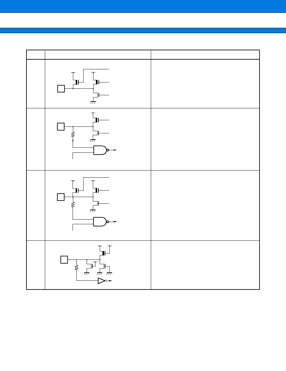
(2) Block Diagram
16-bit reload register
16-bit down-counter
UF
Clock selector
Reload
OUT
CTL
CSL1
CSL0
MOD2
MOD1
MOD0
16
8
16
2
3
2
IN CTL
--
2
--
2
--
2
1
3
5
3
Peripheral clock
Prescaler
Clear
EXCK
GATE
Re-trigger
IRQ
Port (TIN)
Port (TOUT)
Output enable
Serial baud rate
A/DC
RELD
OUTE
OUTL
INTE
UF
CNTE
TRG
Clear
I
2
OSCLR
F
2
MC-16 bus
MB90610A Series
38
6.
Chip Select Function
This module generates chip select signals to simplify connection of memory or I/O devices. The module has 8
chip select output pins. The hardware outputs the chip select signals from the pins when it detects access of an
address in the areas specified in the pin registers.
(1) Register Configuration
(2) Block Diagram
bit
bit
--
--
--
--
ACTL OPEL CSA1 CSA0
Chip select control register
(odd numbers:
CSCR1/3/5/7)
15
14
13
12
11
10
9
8
--
--
--
--
ACTL OPEL CSA1 CSA0
Chip select control register
(even numbers:
CSCR0/2/4/6)
7
6
5
4
3
2
1
0
Address : 000049
H
: 00004B
H
: 00004D
H
: 00004F
H
Address : 000048
H
: 00004A
H
: 00004C
H
: 00004E
H
Selector
Selector
Chip select control register 0
Chip select control register 1
CS0
(For the program
ROM area)
CS1
CS6
Address (from CPU)
Address decoder
Address decoder
A23
A16 A15
A08 A07
A00
Decode signal
Program area
Decode
Selection setting
Selection setting
Selector
Selector
Chip select control register 6
Chip select control register 7
CS7
Selection setting
Selection setting
MB90610A Series
39
7.
DTP/External Interrupts
The DTP (Data Transfer Peripheral) is a peripheral block that interfaces external peripherals to the F
2
MC-16L
CPU. The DTP receives DMA and interrupt processing requests from external peripherals and passes the
requests to the F
2
MC-16L CPU to activate the extended intelligent I/O service or interrupt processing. Two
request levels ("H" and "L") are provided for extended intelligent I/O service. For external interrupt requests,
generation of interrupts on a rising or falling edge as well as on "H", "L" levels can be selected, giving a total of
four types.
(1) Register Configuration
(2) Block Diagram
bit
Read/write
Initial value
EN7
EN6
EN5
EN4
EN3
EN2
EN1
EN0
ENIR
(R/W)
(0)
(R/W)
(0)
(R/W)
(0)
(R/W)
(0)
(R/W)
(0)
(R/W)
(0)
(R/W)
(0)
(R/W)
(0)
7
6
5
4
3
2
1
0
Interrupt/DTP enable register
Address : 000028
H
bit
Read/write
Initial value
ER7
ER6
ER5
ER4
ER3
ER2
ER1
ER0
EIRR
(R/W)
(0)
(R/W)
(0)
(R/W)
(0)
(R/W)
(0)
(R/W)
(0)
(R/W)
(0)
(R/W)
(0)
(R/W)
(0)
15
14
13
12
11
10
9
8
Interrupt/DTP register
Address : 000029
H
bit
Read/write
Initial value
LB7
LA7
LB6
LA6
LB5
LA5
LB4
LA4
(R/W)
(0)
(R/W)
(0)
(R/W)
(0)
(R/W)
(0)
(R/W)
(0)
(R/W)
(0)
(R/W)
(0)
(R/W)
(0)
15
14
13
12
11
10
9
8
Request level setting register (upper)
Address : 00002B
H
bit
Read/write
Initial value
LB3
LA3
LB2
LA2
LB1
LA1
LB0
LA0
ELVR
(R/W)
(0)
(R/W)
(0)
(R/W)
(0)
(R/W)
(0)
(R/W)
(0)
(R/W)
(0)
(R/W)
(0)
(R/W)
(0)
7
6
5
4
3
2
1
0
Request level setting register (lower)
Address : 00002A
H
8
8
8
8
8
Interrupt/DTP enable register
Interrupt/DTP register
Request level setting register
Gate
Request F/F
Edge detect circuit
Request input
Interrupt input
F
2
MC-16 bus
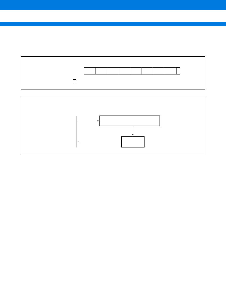
MB90610A Series
40
8.
Delayed Interrupt Generation Module
The delayed interrupt generation module is used to generate the task switching interrupt. Interrupt requests to
the F
2
MC-16L CPU can be generated and cleared by software using this module.
(1) Register Configuration
(2) Block Diagram
bit
Read/write
Initial value
--
--
--
--
--
--
--
R0
DIRR
(--)
(--)
(--)
(--)
(--)
(--)
(--)
(--)
(--)
(--)
(--)
(--)
(--)
(--)
(R/W)
(0)
15
14
13
12
11
10
9
8
Address : 00009F
H
Delayed interrupt generate/
clear decoder
Delayed interrupt generate/clear decoder
Interrupt latch
F
2
MC-16 bus
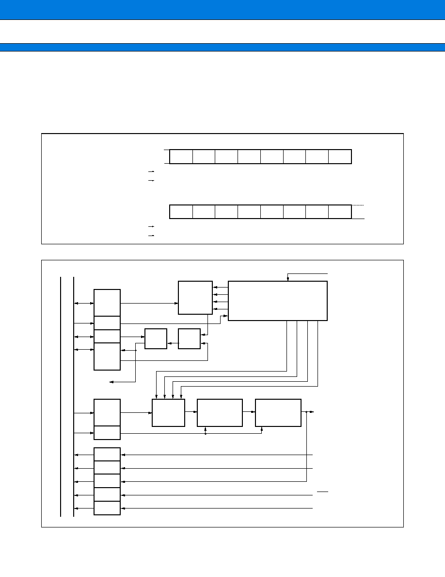
MB90610A Series
41
9.
Watchdog Timer and Timebase Timer Functions
The watchdog timer consists of a 2-bit watchdog counter, a control register, and a watchdog reset controller.
The watchdog counter uses the carry-up signal from the 18-bit timebase timer as its clock source. In addition
to the 18-bit timer, the timebase timer contains an interval interrupt control circuit. The timebase timer uses the
main clock, regardless of the value of the MCS bit in the CKSCR register.
(1) Register Configuration
(2) Block Diagram
bit
Read/write
Initial value
PONR STBR WRST ERST SRST WTE
WT1
WT0
WDTC
(R)
(X)
(R)
(X)
(R)
(X)
(R)
(X)
(R)
(X)
(W)
(1)
(W)
(1)
(W)
(1)
7
6
5
4
3
2
1
0
Watchdog timer control register
Address : 0000A8
H
bit
Read/write
Initial value
Reserved
--
--
TBIE TBOF TBR TBC1 TBC0
TBTC
(--)
(1)
(--)
(--)
(--)
(--)
(R/W)
(0)
(R/W)
(0)
(W)
(1)
(R/W)
(0)
(R/W)
(0)
15
14
13
12
11
10
9
8
Timebase timer control register
Address : 0000A9
H
TBTC
TBC1
TBC0
TBR
TBIE
TBOF
PONR
STBR
WRST
ERST
SRST
Selector
AND
Q
Selector
2-bit counter
CLR
CLR
Watchdog reset
activation circuit
WT1
WDTC
WT0
WTE
2
12
2
12
Timebase
interrupt
S
R
2
14
2
16
2
19
TBTRES
Timebase timer
Clock input
2
14
2
16
2
19
OF
Main clock
(OSC oscillator)
WDGRST
To internal reset
activation circuit
From power-on detection
From hardware standby
control circuit
RST pin
From the RST bit of the
STBYC register
F
2
MC-16 bus
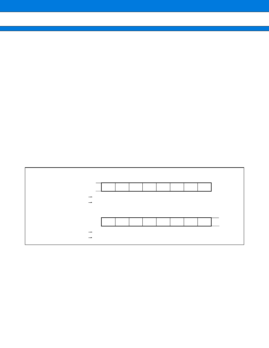
MB90610A Series
42
10. Low Power Control Circuits (CPU Intermittent Operation Function, Oscillation Stabilization
Delay Time, and Clock Multiplier Function)
The following operation modes are available: PLL clock mode, PLL sleep mode, timer mode, main clock mode,
main sleep mode, stop mode, and hardware standby mode. Operation modes other than PLL clock mode are
classified as low power consumption modes.
In main clock mode and main sleep mode, the device operates on the main clock only (OSC oscillator clock).
The PLL clock (VCO oscillator clock) is stopped in these modes and the main clock divided by 2 is used as the
operating clock.
In PLL sleep mode and main sleep mode, the CPU's operating clock only is stopped and other elements continue
to operate.
In timer mode, only the timebase timer operates.
Stop mode and hardware standby mode stop the oscillator. These modes maintain existing data with minimum
power consumption.
The CPU intermittent operation function provides an intermittent clock to the CPU when register, internal memory,
internal resource, or external bus access is performed. This function reduces power consumption by lowering
the CPU execution speed while still providing a high-speed clock to internal resources.
The PLL clock multiplier ratio can be set to 1, 2, 3, 4 by the CS1, 0 bits.
The WS1, 0 bits set the delay time to wait for the main clock oscillation to stabilize when recovering from stop
mode or hardware standby mode.
(1) Register Configuration
bit
Read/write
Initial value
STP
SLP
SPL
RST
Reserved
CG1
CG0
Reserved
LPMCR
(W)
(0)
(W)
(0)
(R/W)
(0)
(W)
(1)
(--)
(1)
(R/W)
(0)
(R/W)
(0)
(--)
(0)
7
6
5
4
3
2
1
0
Low power consumption mode
control register
Address : 0000A0
H
bit
Read/write
Initial value
Reserved
MCM WS1
WS0
Reserved
MCS
CS1
CS0
CKSCR
(--)
(1)
(R)
(1)
(R/W)
(1)
(R/W)
(1)
(--)
(1)
(R/W)
(1)
(R/W)
(0)
(R/W)
(0)
15
14
13
12
11
10
9
8
Clock select register
Address : 0000A1
H
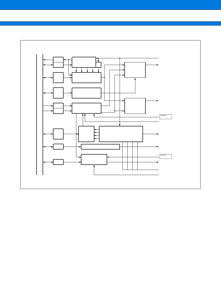
MB90610A Series
43
(2) Block Diagram
Main clock
(OSC oscillator)
MCM
MCS
CS1
CS0
CG1
CG0
SLP
STP
PLL multiplier
circuit
1
2
3
4
1/2
CPU
clock selector
Cycle selection circuit
for the CPU intermittent
operation function
Standby control circuit
RST Release HST activate
WS1
WS0
Oscillation
stabilization
delay time
selector
SPL
Internal reset
generation circuit
RST
Pin high impedance control circuit
CPU clock
generator
Peripheral
clock
generator
Timebase timer
2
4
2
13
2
15
2
18
Clock input
2
19
2
16
2
14
2
12
LPMCR
LPMCR
CKSCR
CKSCR
CKSCR
LPMCR
LPMCR
0/9/17/33
Intermittent
cycle selection
CPU clock
Peripheral clock
HST pin
Interrupt request
or RST
Timebase clock
Pin Hi-Z
RST pin
Internal RST
To watchdog timer
WDGRST
F
2
MC-16 bus
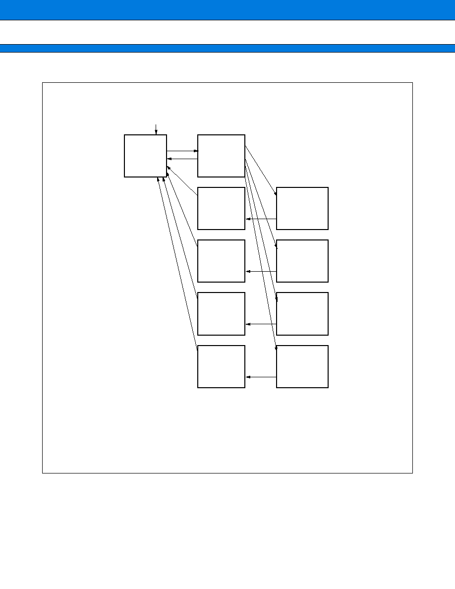
MB90610A Series
44
Main
MCS = 1
MCM = 1
CS1/0 = XX
Main
PLLX
MCS = 0
MCM = 1
CS1/0 = XX
PLL1
Main
MCS = 1
MCM = 0
CS1/0 = 00
PLL2
Main
MCS = 1
MCM = 0
CS1/0 = 01
PLL3
Main
MCS = 1
MCM = 0
CS1/0 = 10
PLL4
Main
MCS = 1
MCM = 0
CS1/0 = 11
PLL multiplier = 1
MCS = 0
MCM = 0
CS1/0 = 00
PLL multiplier = 2
MCS = 0
MCM = 0
CS1/0 = 01
PLL multiplier = 3
MCS = 0
MCM = 0
CS1/0 = 10
PLL multiplier = 4
MCS = 0
MCM = 0
CS1/0 = 11
(1)
(6)
(7)
(7)
(7)
(7)
(2)
(3)
(4)
(6)
(6)
(5)
(6)
(6)
Power-on
(1)
(2)
(3)
(4)
(5)
(6)
(7)
MCS bit cleared
PLL clock oscillation stabilization delay complete and CS1/0 = "00"
PLL clock oscillation stabilization delay complete and CS1/0 = "01"
PLL clock oscillation stabilization delay complete and CS1/0 = "10"
PLL clock oscillation stabilization delay complete and CS1/0 = "11"
MCS bit set (including a hardware standby or watchdog reset)
PLL clock and main clock synchronized timing
∑ State Transition Diagram for Clock Selection
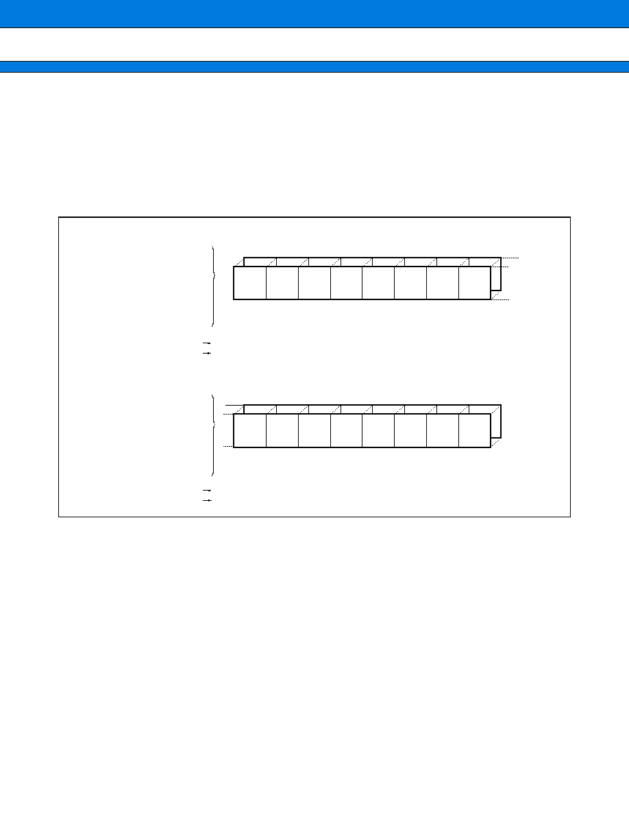
MB90610A Series
45
11. Interrupt Controller
The interrupt control registers are located in the interrupt controller. An interrupt control register is provided for
each I/O with an interrupt function. The registers have the following three functions.
∑ Set the interrupt level of the corresponding peripheral.
∑ Select whether to treat interrupts from the corresponding peripheral as standard interrupts or activate the
extended intelligent I/O service.
∑ Select the extended intelligent I/O service channel.
(1) Register Configuration
Note: Do not access these registers using read-modify-write instructions as this can cause misoperation.
Read/write
Initial value
(W)
(0)
(W)
(0)
(R/W)
(0)
(R/W)
(0)
(R/W)
(0)
(R/W)
(1)
(R/W)
(1)
(R/W)
(1)
bit
15
14
13
12
11
10
9
8
bit
7
6
5
4
3
2
1
0
ICS3 ICS2
ICS1
or
S1
ICS0
or
S0
ISE
IL2
IL1
IL0
ICRxx
ICS3 ICS2
ICS1
or
S1
ICS0
or
S0
ISE
IL2
IL1
IL0
ICRxx
(W)
(0)
(W)
(0)
(R/W)
(0)
(R/W)
(0)
(R/W)
(0)
(R/W)
(1)
(R/W)
(1)
(R/W)
(1)
Read/write
Initial value
Interrupt control register
Address : ICR01 0000B1
H
: ICR03 0000B3
H
: ICR05 0000B5
H
: ICR07 0000B7
H
: ICR09 0000B9
H
: ICR11 0000BB
H
: ICR13 0000BD
H
: ICR15 0000BF
H
Interrupt control register
Address : ICR00 0000B0
H
: ICR02 0000B2
H
: ICR04 0000B4
H
: ICR06 0000B6
H
: ICR08 0000B8
H
: ICR10 0000BA
H
: ICR12 0000BC
H
: ICR14 0000BE
H
MB90610A Series
46
(2) Block Diagram
I S E
I L 2
I L 1
I L 0
Determine priority
of interrupt or I
2
OS
Interrupt/
I
2
OS request
(peripheral resource)
4
4
32
S 1
S 0
Detect I
2
OS
completion condition
I
2
OS completion condition
2
2
2
I C S 3 I C S 2
I C S 1
I C S 0
I
2
OS vector selection
I
2
OS vector
(CPU)
4
4
4
3
(CPU)
Interrupt level
4
I
2
OS selection
F
2
MC-16 bus
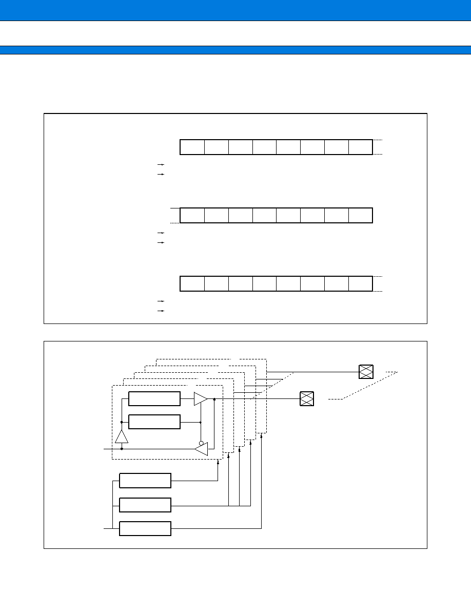
MB90610A Series
47
12. External Bus Terminal Control Circuit
This circuit controls the external bus terminals intended to extend outwardly the CPU's address/data bus.
(1) Register Configuration
(2) Block Diagram
bit
Read/write
Initial value
IOR1 IOR0 HMR1 HMR0
--
--
LMR1 LMR0
ARSR
(W)
(0)
(W)
(0)
(W)
(1)
(W)
(1)
(--)
(--)
(--)
(--)
(W)
(0)
(W)
(0)
15
14
13
12
11
10
9
8
Register for selection of
AUTO ready function
Address : 0000A5
H
bit
Read/write
Initial value
E23
E22
E21
E20
E19
E18
E17
E16
HACR
(W)
(0)
(W)
(0)
(W)
(0)
(W)
(0)
(W)
(0)
(W)
(0)
(W)
(0)
(W)
(0)
7
6
5
4
3
2
1
0
Register for control of
external address output
Address : 0000A6
H
bit
Read/write
Initial value
--
LMBS WRE HMBS IOBS HDE
RYE
CKE
ECSR
(--)
(--)
(W)
(0)
(W)
(0)
(W)
(1/0)
(W)
(0)
(W)
(0)
(W)
(0)
(W)
(0)
15
14
13
12
11
10
9
8
Register for selection of
bus control signal
Address : 0000A7
H
P5
P4
P3
P2
P1
Access control
Data control
P1 data
P1 direction
Access control
Access
control
RB
P5
P1
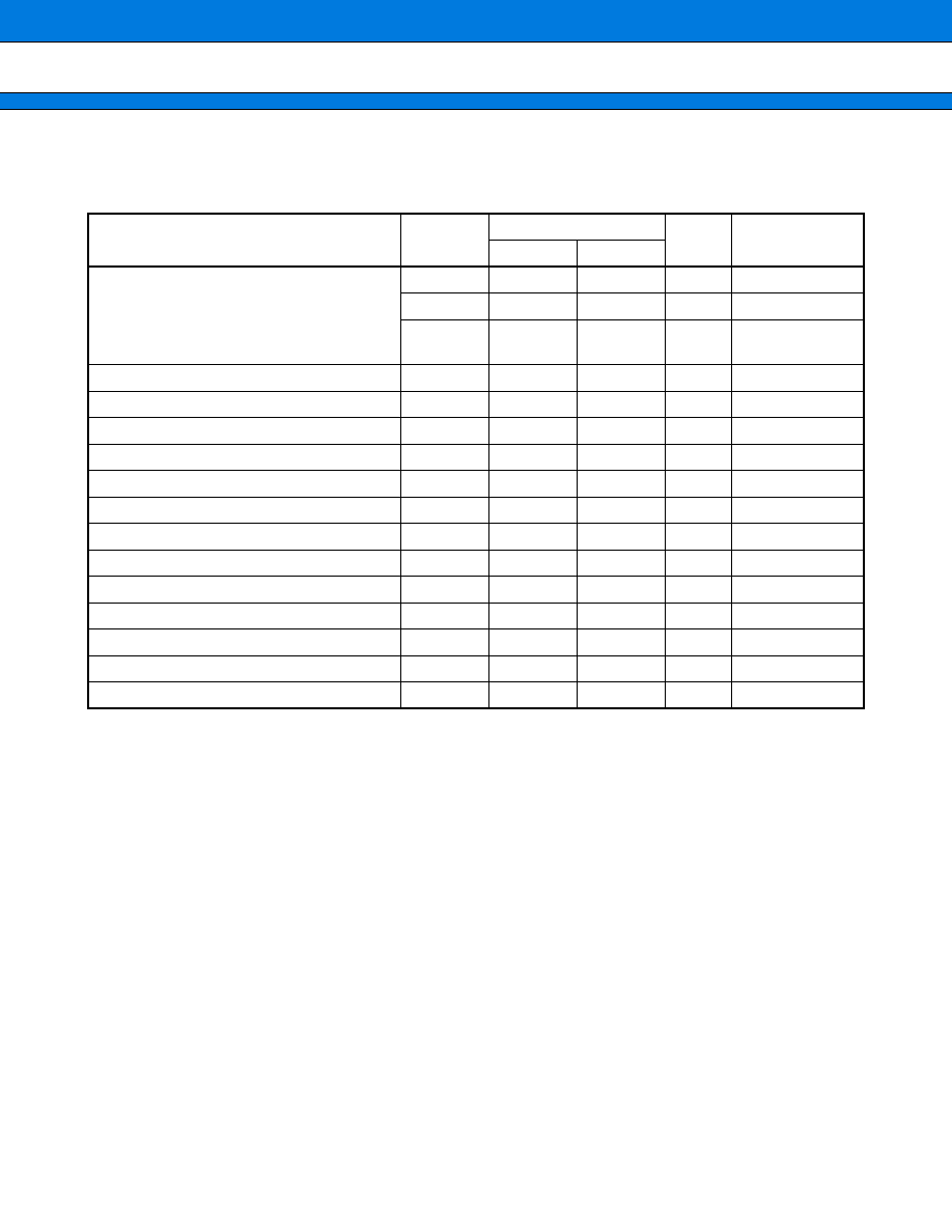
MB90610A Series
48
s
s
s
s
ELECTRICAL CHARACTERISTICS
1.
Absolute Maximum Rating
(V
SS
= AV
SS
= 0.0 V)
*1: AV
CC
, AVRH, and AVRL must not exceed V
CC
. Similarly, it may not exceed AVRL, nor AVRH.
*2: V
I
and V
O
must not exceed V
CC
+ 0.3 V.
*3: The maximum output current must not be exceeded at any individual pin.
*4: The average output current is the rating for the current from an individual pin averaged over a duration of 100 ms.
*5: The average total output current is the rating for the current from all pins averaged over a duration of 100 ms.
WARNING: Semiconductor devices can be permanently damaged by application of stress (voltage, current,
temperature, etc.) in excess of absolute maximum ratings. Do not exceed these ratings.
Parameter
Symbol
Rating
Unit
Remarks
Min.
Max.
Power supply voltage
V
CC
V
SS
≠ 0.3
V
SS
+ 7.0
V
AV
CC
*
1
V
SS
≠ 0.3
V
SS
+ 7.0
V
AVRH*
1
AVRL*
1
V
SS
≠ 0.3
V
SS
+ 7.0
V
Input voltage*
2
V
I
V
SS
≠ 0.3
V
CC
+ 0.3
V
Output voltage*
2
V
O
V
SS
≠ 0.3
V
CC
+ 0.3
V
"L" level maximum output current*
3
I
OL
--
15
mA
"L" level average output current*
4
I
OLAV
--
4
mA
"L" level total maximum output current
I
OL
--
100
mA
"L" level total average output current*
5
I
OLAV
--
50
mA
"H" level maximum output current*
3
I
OH
--
≠15
mA
"H" level average output current*
4
I
OHAV
--
≠4
mA
"H" level total maximum output current
I
OH
--
≠100
mA
"H" level total average output current*
5
I
OHAV
--
≠50
mA
Power consumption
P
d
--
+400
mW
Operating temperature
T
A
≠40
+85
∞C
Storage temperature
T
stg
≠55
+150
∞C
MB90610A Series
49
2.
Recommended Operating Conditions
(V
SS
= 0.0 V)
WARNING: The recommended operating conditions are required in order to ensure the normal operation of the
semiconductor device. All of the device's electrical characteristics are warranted when the device is
operated within these ranges.
Always use semiconductor devices within their recommended operating condition ranges. Operation
outside these ranges may adversely affect reliability and could result in device failure.
No warranty is made with respect to uses, operating conditions, or combinations not represented on
the data sheet. Users considering application outside the listed conditions are advised to contact their
FUJITSU representatives beforehand.
Parameter
Symbol
Rating
Unit
Remarks
Min.
Max.
Power supply voltage
V
CC
2.7
5.5
V
For normal operation
2.0
5.5
V
To maintain statuses in stop mode
Operating temperature
T
A
≠40
+85
∞C
MB90610A Series
50
3.
DC Characteristics
(V
CC
= +2.7 V to +5.5 V, V
SS
= 0.0 V, T
A
= ≠40∞C to +85∞C)
*1: Hysteresis input pins: RST, HST, P60 to P67, P70 to P76, P80 to P86, P90 to P95, PA1 to PA7
*2: TTL input pins: AD00/D00 to AD07/D07, AD08/D08/P10 to AD15/D15/P17, HRQ/P53, RDY/P51
Parameter
Sym-
bol
Pin name
Conditions
Value
Unit
Re-
marks
Min.
Typ.
Max.
"H" level input
voltage
V
IH
--
--
0.7 V
CC
--
V
CC
+ 0.3
V
V
IHS
0.8 V
CC
--
V
CC
+ 0.3
V
*1
V
IHM
V
CC
≠ 0.3
--
V
CC
+ 0.3
V
V
IHT
V
CC
= +5.0 V±10%
2.2
--
--
V
*2
V
CC
= +3.0 V±10%
0.7 V
CC
--
--
V
*2
"L" level input
voltage
V
IL
--
V
SS
≠ 0.3
--
0.3 V
CC
V
V
ILS
V
SS
≠ 0.3
--
0.2 V
CC
V
*1
V
ILM
V
SS
≠ 0.3
--
V
SS
+ 0.3
V
V
ILT
V
CC
= +5.0 V±10%
V
SS
≠ 0.3
--
0.8
V
*2
V
CC
= +3.0 V±10%
V
SS
≠ 0.3
--
0.2 V
CC
V
*2
"H" level output
voltage
V
OH
Other than P60
to P67
V
CC
= +5.0 V±10%
I
OH
= ≠4.0 mA
V
CC
≠ 0.5
--
--
V
V
CC
= +3.0 V±10%
I
OH
= ≠1.6 mA
V
CC
≠ 0.3
--
--
V
"L" level output
voltage
V
OL
All output pins
V
CC
= +5.0 V±10%
I
OL
= ≠4.0 mA
--
--
0.4
V
V
CC
= +3.0 V±10%
I
OL
= ≠2.0 mA
--
--
0.4
V
Pull-up resis-
tance
R
pu
RST, P50 to
P55,
RD, ALE,
PA1 to PA7,
CS0
--
30
--
100
k
Supply current
I
CC
V
CC
V
CC
= +5.0 V±10%
16 MHz internal op-
eration
--
50
70
mA
I
CCS
--
25
30
mA
I
CC
V
CC
= +3.0 V±10%
8 MHz internal op-
eration
--
10
20
mA
I
CCS
--
5
10
mA
I
CCH
V
CC
= +5.0 V±10%
T
A
= 25∞C
--
0.1
10
µ
A
Input pin capaci-
tance
C
IN
Other than
AV
CC
, AV
SS
,
V
CC
,V
SS
--
--
10
--
pF
Input leakage cur-
rent
I
IL
Other than P60
to P67
V
CC
= 5.5 V
V
SS
< V
I
< V
CC
≠10
--
10
µ
A
Leakage current
for open drain
outputs
I
leak
Other than P60
to P67
--
--
0.1
10
µ
A
Pull-down resis-
tance
R
pd
MD2
--
40
--
200
k
MB90610A Series
51
4.
AC Characteristics
(1) Clock Timing
∑ When V
CC
= +5.0 V±10%
(V
CC
= +4.5 V to +5.5 V, V
SS
= 0.0 V, T
A
= ≠40∞C to +85∞C)
*The frequency variation ratio is the maximum variation from the specified central frequency when the multiplier
PLL is locked. The value is expressed as a proportion.
∑ When V
CC
= +2.7 V (min.)
(V
CC
= +2.7 V to +5.5 V, V
SS
= 0.0 V, T
A
= ≠40∞C to +85∞C)
Parameter
Sym-
bol
Pin name
Conditions
Value
Unit
Remarks
Min.
Max.
Clock frequency
f
C
X0, X1
--
3
32
MHz
Clock cycle time
t
C
X0, X1
--
31.25
333
ns
Frequency variation ratio*
(when locked)
f
--
--
--
3
%
Input clock pulse width
P
WH
P
WL
X0
--
10
--
ns
The duty ratio
should be in the
range 30 to 70%
Input clock rise time and fall
time
t
cr
t
cf
X0
--
--
5
ns
Internal operating clock fre-
quency
f
CP
--
--
1.5
16
MHz
Internal operating clock cy-
cle time
t
CP
--
--
62.5
666
ns
Parameter
Sym-
bol
Pin name
Conditions
Value
Unit
Remarks
Min.
Max.
Clock frequency
f
C
X0, X1
--
3
16
MHz
Clock cycle time
t
C
X0, X1
--
62.5
333
ns
Input clock pulse width
P
WH
P
WL
X0
--
20
--
ns
The duty ratio
should be in the
range 30 to 70%
Input clock rise time and fall
time
t
cr
t
cf
X0
--
--
5
ns
Internal operating clock fre-
quency
f
CP
--
--
1.5
8
MHz
Internal operating clock cy-
cle time
t
CP
--
--
125
666
ns
f =
◊
100 (%)
f
0
Central frequency f
0
+
-
MB90610A Series
52
0.8 V
CC
0.2 V
CC
t
C
t
cf
t
cr
P
WH
P
WL
∑ Clock Timing
5.5
4.5
2.7
8
16
f
CP
(MHz)
Normal operation range
3.3
3
1.5
PLL operation assurance range
Internal clock
3 4
8
16
24
32
16
12
9
8
4
Multiply
by 3
Multiply
by 4
No multiplier
Oscillation clock f
C
(MHz)
Relationship between the oscillation frequency and internal operating clock frequency
Relationship between the internal operating clock frequency and supply voltage
Multiply by 1
Multiply by 2
Note: Low voltage operation down to 2.7V is also assured for the evaluation tools.
Power supply V
CC
(V)
Internal Clock f
CP
(MHz)
∑ PLL Operation Assurance Range
MB90610A Series
53
The AC characteristics are for the following measurement reference voltages.
(2) Clock Output Timing
(V
CC
= +2.7 V to +5.5 V, V
SS
= 0.0 V, T
A
= ≠40∞C to +85∞C)
Parameter
Sym-
bol
Pin
name
Conditions
Value
Unit
Remarks
Min.
Max.
Cycle time
t
CYC
CLK
V
CC
= +5 V±10%
t
CP
--
ns
CLK
CLK
t
CHCL
t
CP
/2 ≠ 20
t
CP
/2 + 20
ns
Hysteresis input pins
0.8 V
CC
0.2 V
CC
Other than hysteresis/MD input pins
0.7 V
CC
0.3 V
CC
Output pins
2.4 V
0.8 V
∑ Input Signal Waveform
∑ Output Signal Waveform
t
CYC
t
CHCL
CLK
0.8 V
2.4 V
2.4 V
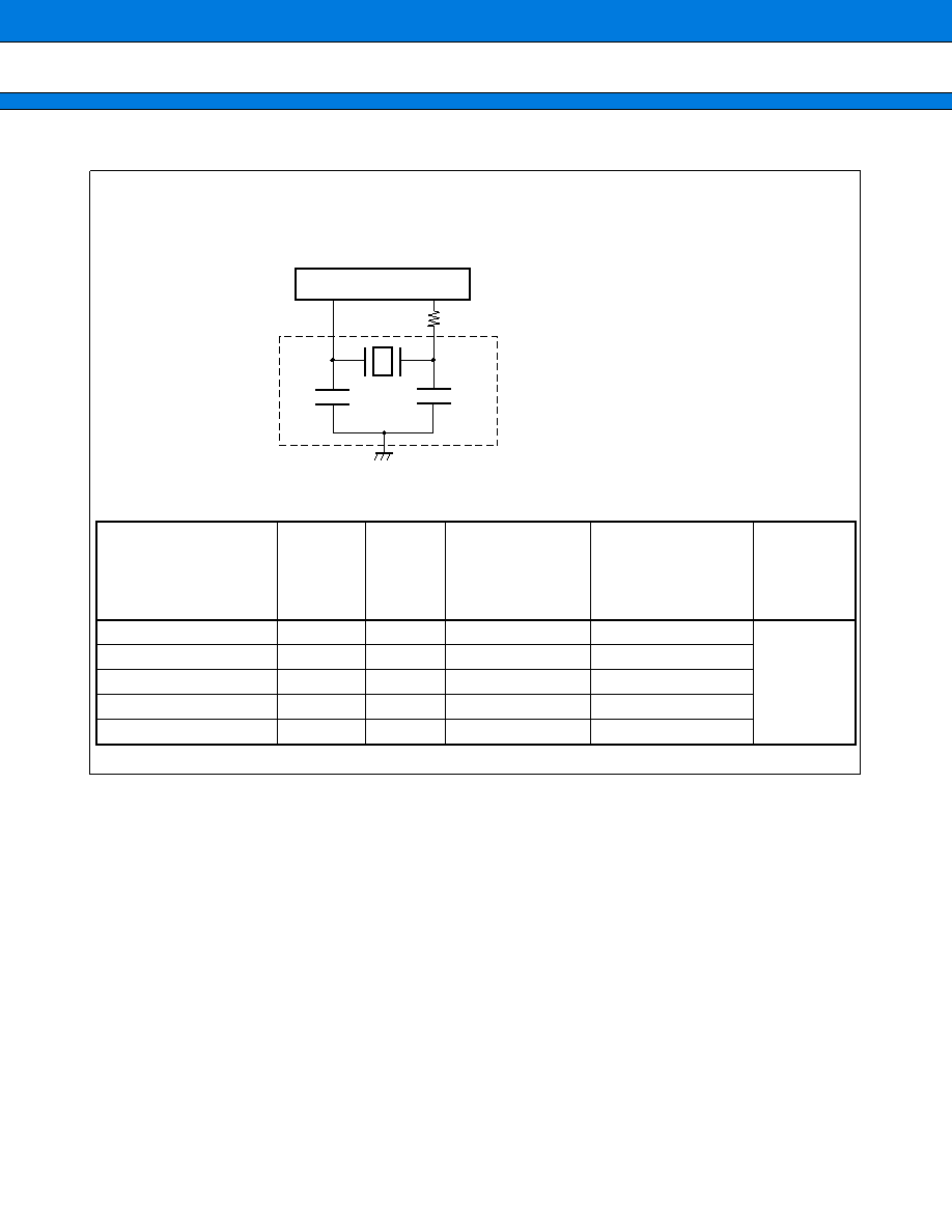
MB90610A Series
54
(3) Recommended Resonator Manufacturers
X 0
X 1
C 1
C 2
*2
*2
FAR
*1: Fujitsu Acoustic Resonator
*1
R
Inquiry: FUJITSU LIMITED
FAR part number
(built-in capacitor type)
Frequency
(MHz)
Dumping
resistor
Initial deviation of
FAR frequency
(T
A
= +25
∞
C)
Temperature
characteristics of
FAR frequency
(T
A
= ≠20
∞
C to +60
∞
C)
Loading ca-
pacitors*
2
FAR-C4CC-02000-L20
2.00
1 k
±
0.5%
±
0.5%
Built-in
FAR-C4CA-04000-M01
4.00
--
±
0.5%
±
0.5%
FAR-C4CB-08000-M02
8.00
--
±
0.5%
±
0.5%
FAR-C4CB-10000-M02
10.00
--
±
0.5%
±
0.5%
FAR-C4CB-16000-M02
16.00
--
±
0.5%
±
0.5%
∑ Sample Application of Piezoelectric Resonator (FAR Family)
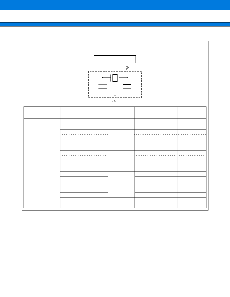
MB90610A Series
55
(Continued)
X 0
X 1
C 1
C 2
*3
*2
*1
R
*4
∑ Sample Application of Ceramic Resonator
Resonator
manufacturer*
1
Resonator
Frequency
(MHz)
C1 (pF)*
2
C2 (pF)*
3
R*
4
Kyocera Corpora-
tion
KBR-2.0MS
2.00
150
150
Not required
PBRC2.00A
150
150
Not required
KBR-4.0MSA
4.00
33
33
680
KBR-4.0MKS
Built-in
Built-in
680
PBRC4.00A
33
33
680
PBRC4.00B
Built-in
Built-in
680
KBR-6.0MSA
6.00
33
33
Not required
KBR-6.0MKS
Built-in
Built-in
Not required
PBRC6.00A
33
33
Not required
PBRC6.00B
Built-in
Built-in
Not required
KBR-8.0M
8.00
33
33
560
PBRC8.00A
33
33
Not required
PBRC8.00B
Built-in
Built-in
Not required
KBR-10.0M
10.00
33
33
330
PBRC10.00B
Built-in
Built-in
680
KBR-12.0M
12.00
33
33
330
PBRC12.00B
Built-in
Built-in
680
MB90610A Series
56
(Continued)
Inquiry: Kyocera Corporation
∑
AVX Corporation
North American Sales Headquarters: TEL 1-803-448-9411
∑
AVX Limited
European Sales Headquarters: TEL 44-1252-770000
∑
AVX/Kyocera H.K. Ltd.
Asian Sales Headquarters: TEL 852-363-3303
Murata Mfg. Co., Ltd.
∑
Murata Electronics North America, Inc.: TEL 1-404-436-1300
∑
Murata Europe Management GmbH: TEL 49-911-66870
∑
Murata Electronics Singapore (Pte.) Ltd.: TEL 65-758-4233
Resonator
manufacturer*
1
Resonator
Frequency
(MHz)
C1 (pF)*
2
C2 (pF)*
3
R*
4
Murata Mfg. Co.,
Ltd.
CSA2.00MG040
2.00
100
100
Not required
CST2.00MG040
Built-in
Built-in
Not required
CSA4.00MG040
4.00
100
100
Not required
CST4.00MGW040
Built-in
Built-in
Not required
CSA6.00MG
6.00
30
30
Not required
CST6.00MGW
Built-in
Built-in
Not required
CSA8.00MTZ
8.00
30
30
Not required
CST8.00MTW
Built-in
Built-in
Not required
CSA10.00MTZ
10.00
30
30
Not required
CST10.00MTW
Built-in
Built-in
Not required
CSA12.00MTZ
12.00
30
30
Not required
CST12.00MTW
Built-in
Built-in
Not required
CSA16.00MXZ040
16.00
15
15
Not required
CST16.00MXW0C3
Built-in
Built-in
Not required
CSA20.00MXZ040
20.00
10
10
Not required
CSA24.00MXZ040
24.00
5
5
Not required
CSA32.00MXZ040
32.00
5
5
Not required
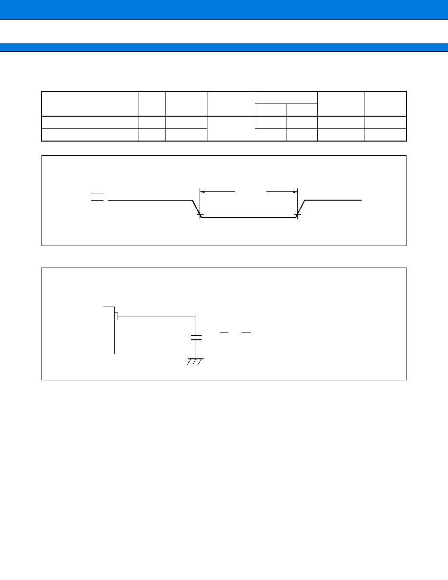
MB90610A Series
57
(4) Reset and Hardware Standby Inputs
(V
CC
= +2.7 V to +5.5 V, V
SS
= 0.0 V, T
A
= ≠40∞C to +85∞C)
Parameter
Sym-
bol
Pin name
Conditions
Value
Unit
Remarks
Min.
Max.
Reset input time
t
RSTL
RST
--
16 t
CP
--
ns
Hardware standby input time t
HSTL
HST
16 t
CP
--
ns
RST
HST
0.2 V
CC
0.2 V
CC
t
RSTL
,
t
HSTL
C
L
Pin
C
L
: Load capacity during testing
For CLK and ALE, C
L
= 30 pF.
For address and data buses (AD15 to AD00),
RD and WR, C
L
= 80 pF.
∑ Conditions for Measurement of AC Reference
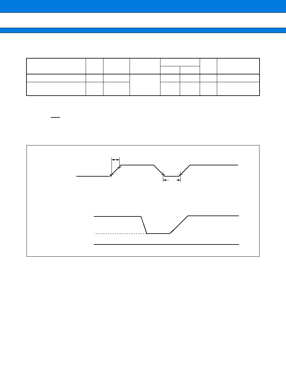
MB90610A Series
58
(5) Power-on Reset
(V
CC
= +2.7 V to +5.5 V, V
SS
= 0.0 V, T
A
= ≠40∞C to +85∞C)
*V
CC
should be lower than 0.2 V before power supply rise.
Notes:
∑ The above values are the values required for a power-on reset
∑ When HST = "L", this standard must be followed to turn on power supply for power-on reset whether or not
necessary.
∑ The device has built-in registers which are initialized only by power-on reset. For possible initialization of these
registers, turn on power supply according to this standard.
Parameter
Sym-
bol
Pin name
Conditions
Value
Unit
Remarks
Min.
Max.
Power supply rise time
t
R
V
CC
--
--
30
ms
*
Power supply cut-off time
t
OFF
V
CC
1
--
ms
For repetition of the
operation
2.7 V
t
R
0.2 V
0.2 V
V
CC
Main power supply voltage
Sub power supply voltage
V
SS
The gradient should be no
more than 50mV/ms.
Abrupt changes in the power supply voltage may cause a power-on reset.
When changing the power supply voltage during operation, the change should be
as smooth as possible, as shown in the following figure.
t
OFF
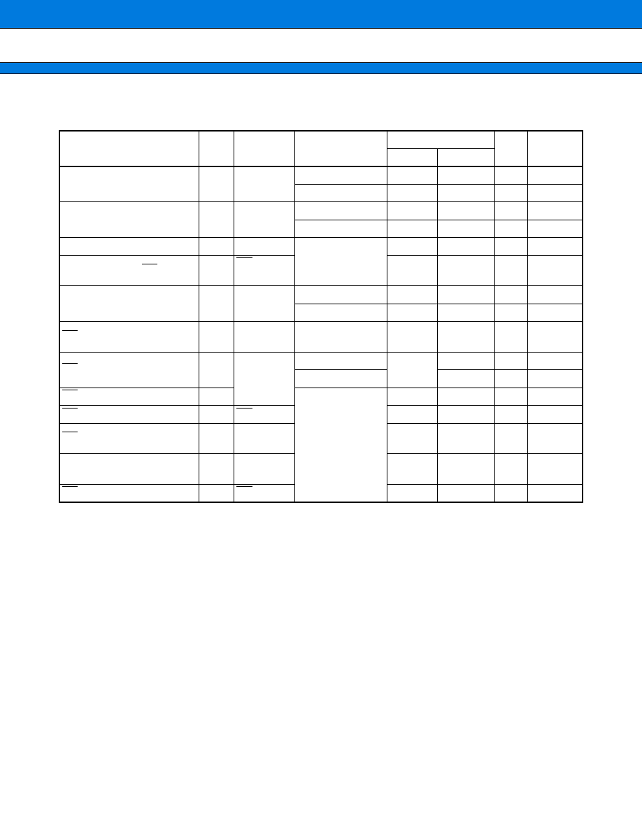
MB90610A Series
59
(6) Bus Timing (Read)
(V
CC
= +2.7 V to +5.5 V, V
SS
= 0.0 V, T
A
= ≠40∞C to +85∞C)
Parameter
Sym-
bol
Pin name
Conditions
Value
Unit
Remarks
Min.
Max.
ALE pulse width
t
LHLL
ALE
V
CC
= +5.0 V±10% t
CP
/2 ≠ 20
--
ns
V
CC
= +3.0 V±10% t
CP
/2 ≠ 35
--
ns
Valid address
ALE
time t
AVLL
Address
V
CC
= +5.0 V±10% t
CP
/2 ≠ 20
--
ns
V
CC
= +3.0 V±10% t
CP
/2 ≠ 40
--
ns
ALE
address valid time
t
LLAX
Address
--
t
CP
/2 ≠ 15
--
ns
Valid address
RD
time
t
AVRL
RD,
Address
t
CP
≠ 15
--
ns
Valid address
valid data
input
t
AVDV
Address/
data
V
CC
= +5.0 V±10%
--
5 t
CP
/2 ≠ 60
ns
V
CC
= +3.0 V±10%
--
5 t
CP
/2 ≠ 80
ns
RD pulse width
t
RLRH
RD
--
3 t
CP
/2 ≠
20
--
ns
RD
valid data input
t
RLDV
Data
V
CC
= +5.0 V±10%
--
3 t
CP
/2 ≠ 60
ns
V
CC
= +3.0 V±10%
3 t
CP
/2 ≠ 80
ns
RD
data hold time
t
RHDX
--
0
--
ns
RD
ALE
time
t
RHLH
RD, ALE
t
CP
/2 ≠ 15
--
ns
RD
address valid time
t
RHAX
Address,
RD
t
CP
/2 ≠ 10
--
ns
Valid address
CLK
time t
AVCH
Address,
CLK
t
CP
/2 ≠ 20
--
ns
RD
CLK
time
t
RLCH
RD, CLK
t
CP
/2 ≠ 20
--
ns
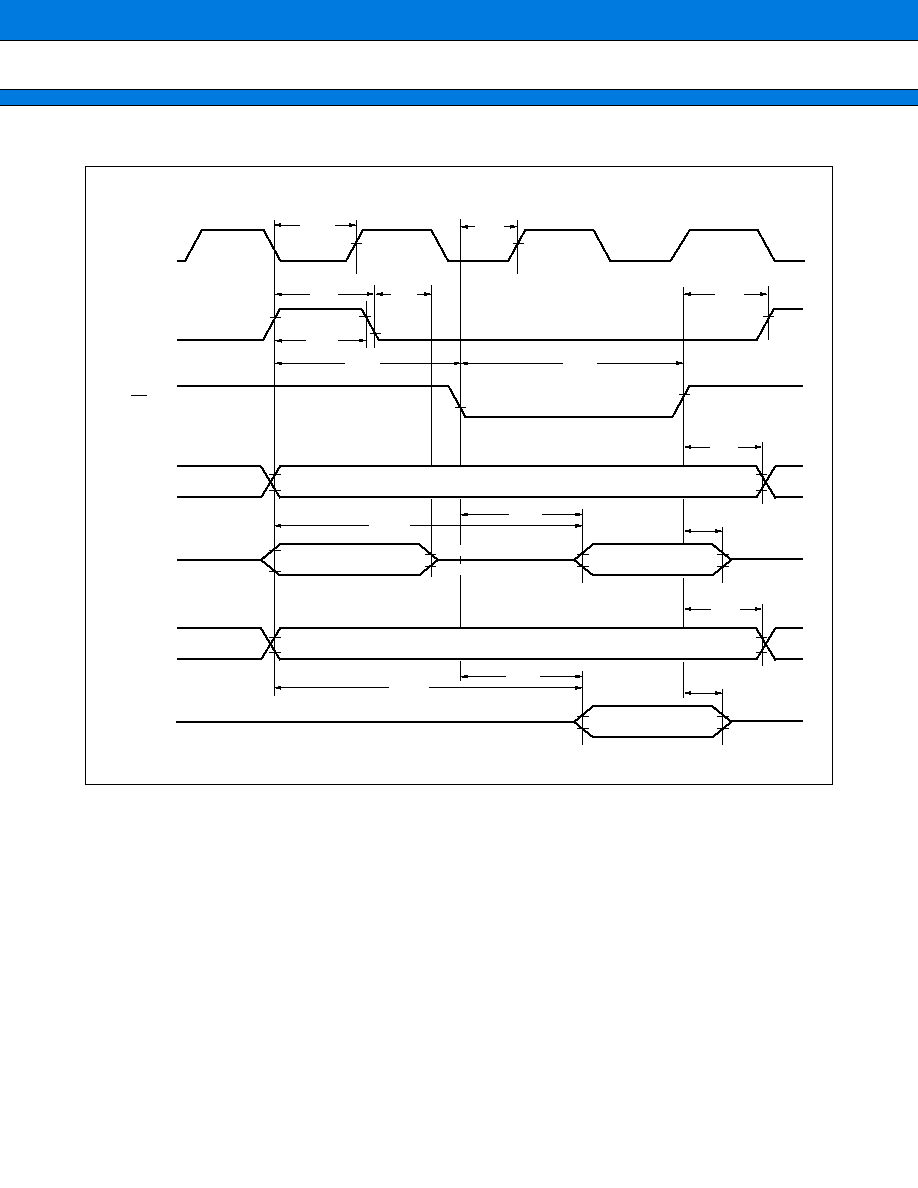
MB90610A Series
60
CLK
ALE
RD
Address
Read data
t
LHLL
t
AVRL
t
RLRH
t
RHAX
t
RHDX
2.4 V
2.4 V
2.4 V
0.8 V
2.4 V
2.4 V
0.8 V
2.4 V
0.8 V
2.4 V
0.8 V
2.4 V
0.8 V
2.4 V
2.2 V
2.2 V
0.8 V
A23 to
A16
D15 to
D00
Multiplex mode
0.8 V
Read data
t
RHAX
t
RHDX
t
AVDV
t
RLDV
0.8 V
2.4 V
0.8 V
2.4 V
2.2 V
2.2 V
0.8 V
A23 to
A00
Non-multiplex mode
0.8 V
0.8 V
2.4 V
t
AVCH
t
RLCH
t
AVLL
t
LLAX
t
RHLH
t
AVDV
t
RLDV
t
AVDV
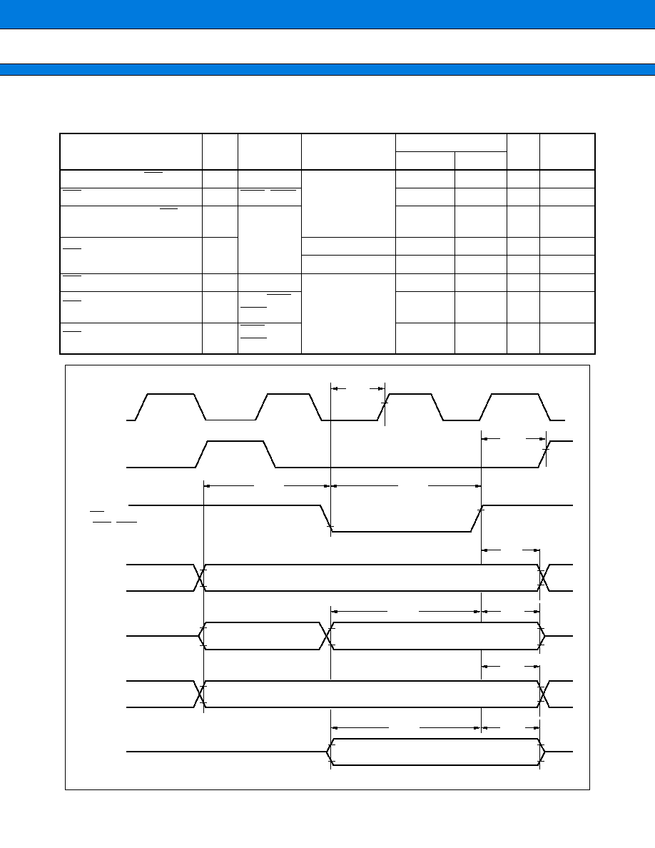
MB90610A Series
61
(7) Bus Timing (Write)
(V
CC
= +2.7 V to +5.5 V, V
SS
= 0.0 V, T
A
= ≠40∞C to +85∞C)
Parameter
Sym-
bol
Pin name
Conditions
Value
Unit
Remarks
Min.
Max.
Valid address
WR
time
t
AVWL
Address
--
t
CP
≠ 15
--
ns
WR pulse width
t
WLWH
WRL, WRH
3 t
CP
/2 ≠ 20
--
ns
Valid data output
WR
time
t
DVWH
Data
3 t
CP
/2 ≠ 20
--
ns
WR
data hold time
t
WHDX
V
CC
= +5.0 V±10%
20
--
ns
V
CC
= +3.0 V±10%
30
--
ns
WR
address valid time
t
WHAX
Address
--
t
CP
/2 ≠ 10
--
ns
WR
ALE
time
t
WHLH
ALE, WRL,
WRH
t
CP
/2 ≠ 15
--
ns
WR
CLK
time
t
WLCH
WRL,
WRH, CLK
t
CP
/2 ≠ 20
--
ns
CLK
ALE
WR
(WRL, WRH)
Address
Write data
t
WHDX
t
WHAX
t
WLWH
t
AVWL
0.8 V
2.4 V
A23 to
A16
AD15 to
AD00
2.4 V
2.4 V
2.4 V
0.8 V
2.4 V
0.8 V
2.4 V
0.8 V
2.4 V
0.8 V
2.4 V
0.8 V
Multiplex mode
Write data
t
WHDX
A23 to
A00
D15 to
D00
2.4 V
0.8 V
2.4 V
0.8 V
2.4 V
0.8 V
2.4 V
0.8 V
Non-multiplex mode
t
WLCH
t
WHLH
t
WHDX
t
WHAX
t
DVWH
t
DVWH
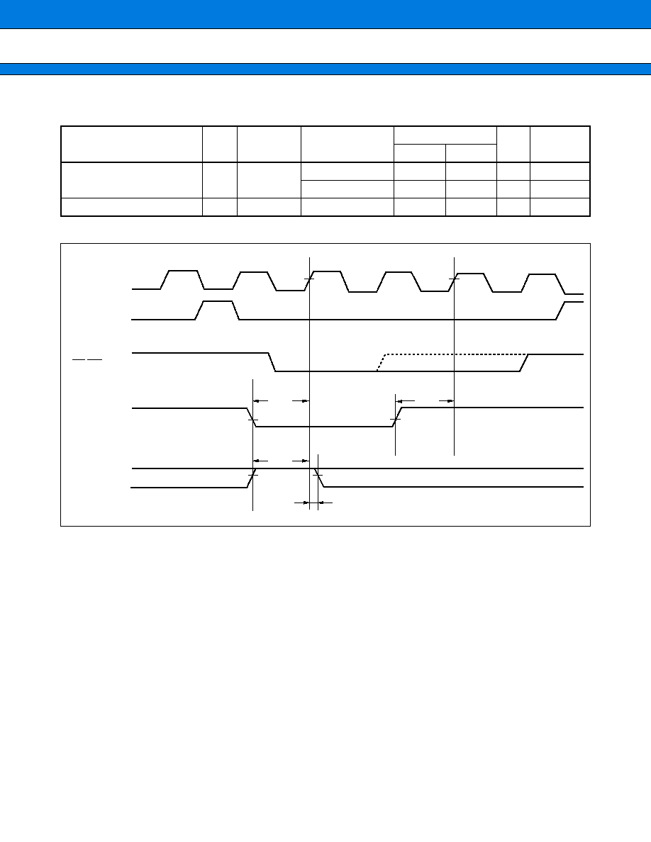
MB90610A Series
62
(8) Ready Input Timing
(V
CC
= +2.7 V to +5.5 V, V
SS
= 0.0 V, T
A
= ≠40∞C to +85∞C)
Note: Use the auto-ready function if the setup time at fall of the RDY is too short.
Parameter
Sym-
bol
Pin name
Conditions
Value
Unit
Remarks
Min.
Max.
RDY setup time
t
RYHS
RDY
V
CC
= +5.0 V±10%
45
--
ns
V
CC
= +3.0 V±10%
70
--
ns
RDY hold time
t
RYHH
RDY
--
0
--
ns
CLK
ALE
RDY
(Wait cycle)
RDY
(No wait cycle)
RD/WR
2.4 V
2.4 V
t
RYHS
t
RYHS
t
RYHS
t
RYHH
0.2 V
CC
0.2 V
CC
0.8 V
CC
0.8 V
CC
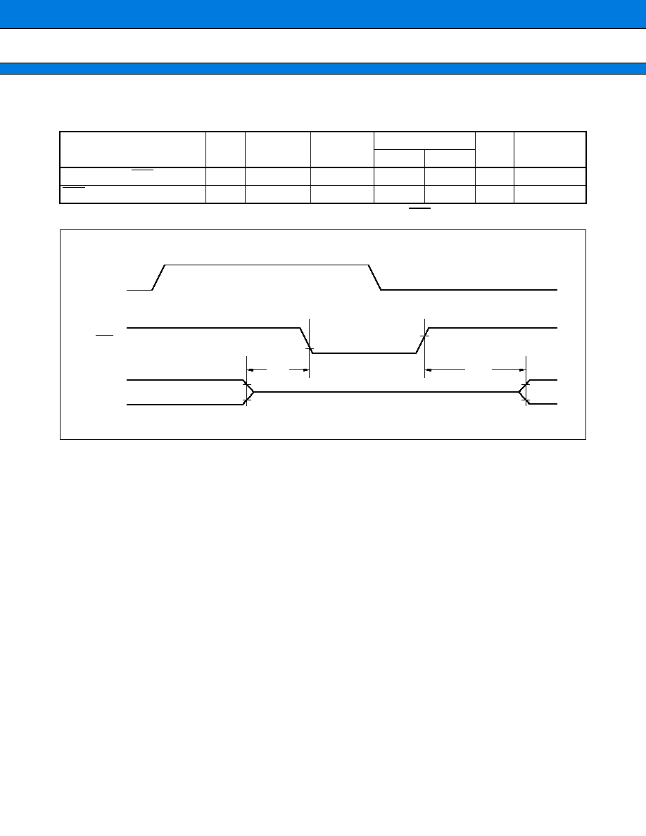
MB90610A Series
63
(9) Hold Timing
(V
CC
= +2.7 V to +5.5 V, V
SS
= 0.0 V, T
A
= ≠40∞C to +85∞C)
Note: After reading HRQ, more than one cycle is required before changing HAK.
Parameter
Sym-
bol
Pin name
Conditions
Value
Unit
Remarks
Min.
Max.
Pin floating
HAK
time
t
XHAL
HAK
--
30
t
CP
ns
HAK
pin valid time
t
HAHV
HAK
--
t
CP
2 t
CP
ns
HRQ
High impedance
HAK
Pin
0.8 V
2.4 V
t
XHAL
t
HAHV
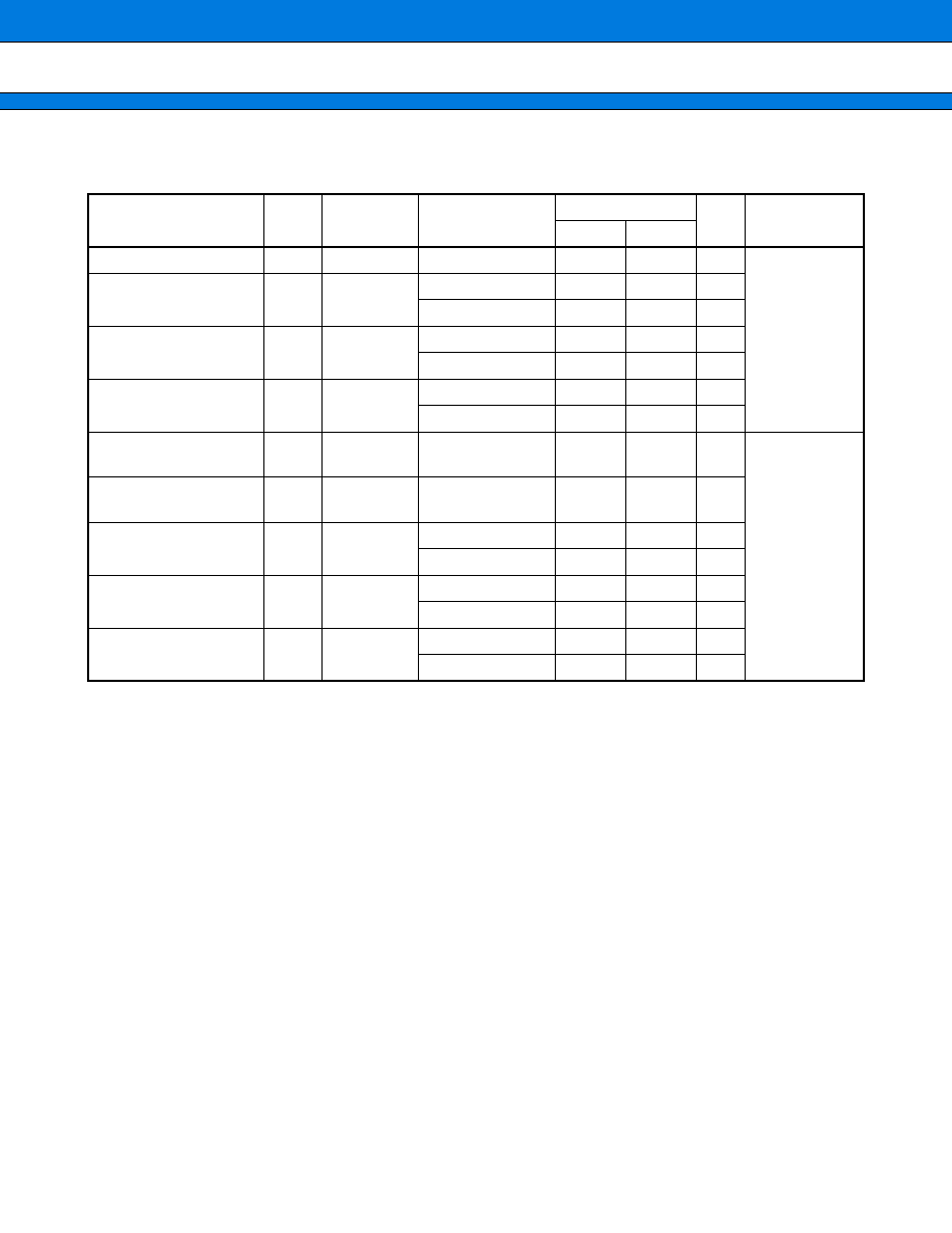
MB90610A Series
64
(10) I/O Expansion Serial Timing
(V
CC
= +2.7 V to +5.5 V, V
SS
= 0.0 V, T
A
= ≠40∞C to +85∞C)
Notes:
∑ These are the AC characteristics for CLK synchronous mode.
∑ C
L
is the load capacitance connected to the pin at testing.
∑ t
CP
is the machine cycle period (unit: ns).
Parameter
Sym-
bol
Pin name
Conditions
Value
Unit
Remarks
Min.
Max.
Serial clock cycle time
t
SCYC
SCK0 to 2
--
8 t
CP
--
ns
C
L
= 80 pF + 1
TTL for the in-
ternal shift clock
mode output
pin.
SCK
SOT delay
time
t
SLOV
SCK0 to 2
SOT0 to 2
V
CC
= +5.0 V±10%
≠80
80
ns
V
CC
= +3.0 V±10%
≠120
120
ns
Valid SIN
SCK
t
IVSH
SCK0 to 2
SIN0 to 2
V
CC
= +5.0 V±10%
100
--
ns
V
CC
= +3.0 V±10%
200
--
ns
SCK
valid SIN hold
time
t
SHIX
SCK0 to 2
SIN0 to 2
V
CC
= +5.0 V±10%
60
--
ns
V
CC
= +3.0 V±10%
120
--
ns
Serial clock "H" pulse
width
t
SHSL
SCK0 to 2
--
4 t
CP
--
ns
C
L
= 80 pF + 1
TTL for the ex-
ternal shift clock
mode output
pin.
Serial clock "L" pulse
width
t
SLSH
SCK0 to 2
--
4 t
CP
--
ns
SCK
SOT delay
time
t
SLOV
SCK0 to 2
SOT0 to 2
V
CC
= +5.0 V±10%
--
150
ns
V
CC
= +3.0 V±10%
--
200
ns
Valid SIN
SCK
t
IVSH
SCK0 to 2
SIN0 to 2
V
CC
= +5.0 V±10%
60
--
ns
V
CC
= +3.0 V±10%
120
--
ns
SCK
valid SIN hold
time
t
SHIX
SCK0 to 2
SIN0 to 2
V
CC
= +5.0 V±10%
60
--
ns
V
CC
= +3.0 V±10%
120
--
ns
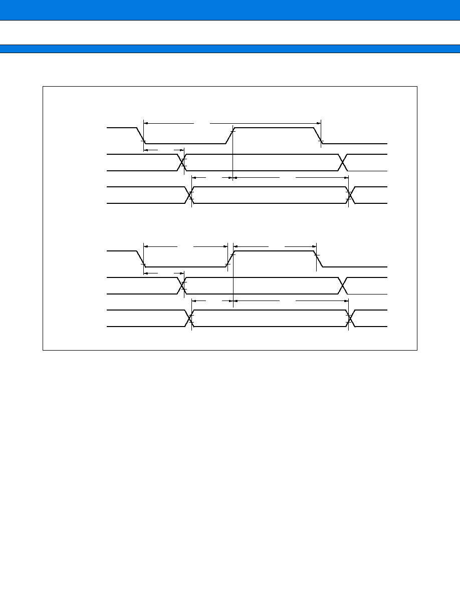
MB90610A Series
65
SCK
SOT
SIN
t
SCYC
t
SLOV
t
IVSH
t
SHIX
2.4 V
0.8 V
CC
0.8 V
0.8 V
2.4 V
0.8 V
0.2 V
CC
0.8 V
CC
0.2 V
CC
SCK
SOT
SIN
t
SLSH
t
SLOV
t
IVSH
t
SHIX
t
SHSL
0.8 V
CC
2.4 V
0.2 V
CC
0.8 V
CC
0.2 V
CC
0.8 V
0.8 V
CC
0.2 V
CC
0.2 V
CC
0.8 V
CC
∑ Internal Shift Clock Mode
∑ External Shift Clock Mode
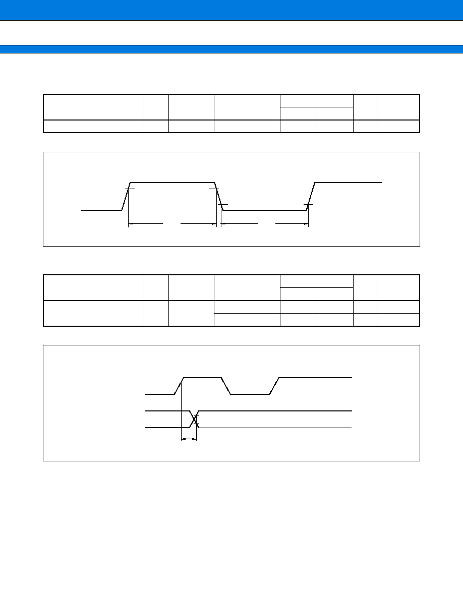
MB90610A Series
66
(11) Timer Input Timing
(V
CC
= +2.7 V to +5.5 V, V
SS
= 0.0 V, T
A
= ≠40∞C to +85∞C)
(12) Timer Output Timing
(V
CC
= +2.7 V to +5.5 V, V
SS
= 0.0 V, T
A
= ≠40∞C to +85∞C)
Parameter
Sym-
bol
Pin name
Conditions
Value
Unit
Remarks
Min.
Max.
Input pulse width
t
TIWH/L
TIN0 to 1
--
4 t
CP
--
ns
Parameter
Sym-
bol
Pin name
Conditions
Value
Unit
Remarks
Min.
Max.
CLK
T
OUT
change timing t
TO
TOT0 to 1
V
CC
= +5.0 V±10%
30
--
ns
V
CC
= +3.0 V±10%
80
--
ns
0.8 V
CC
0.2 V
CC
t
TIWH
0.2 V
CC
0.8 V
CC
t
TIWL
∑ Timer Input Timing
CLK
T
OUT
t
TO
2.4 V
CC
2.4 V
0.8 V
CC
∑ Timer Output Timing
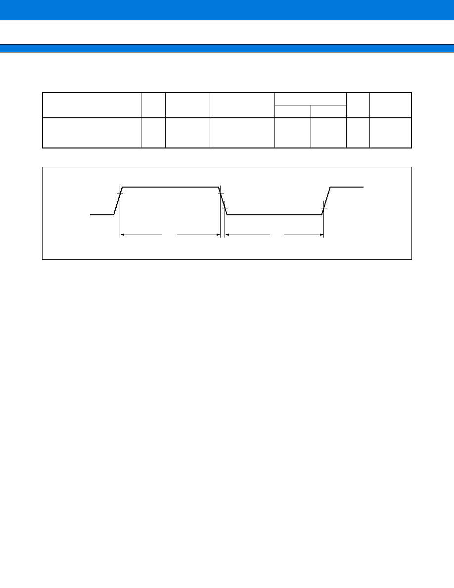
MB90610A Series
67
(13) Trigger Input Timing
(V
CC
= +2.7 V to +5.5 V, V
SS
= 0.0 V, T
A
= ≠40∞C to +85∞C)
Parameter
Sym-
bol
Pin name
Conditions
Value
Unit
Remarks
Min.
Max.
Input pulse width
t
TRGH
t
TRGL
ATG
INT0 to
INT1
--
5 t
CP
--
ns
0.8 V
CC
0.8 V
CC
0.2 V
CC
0.2 V
CC
t
TRGH
t
TRGL
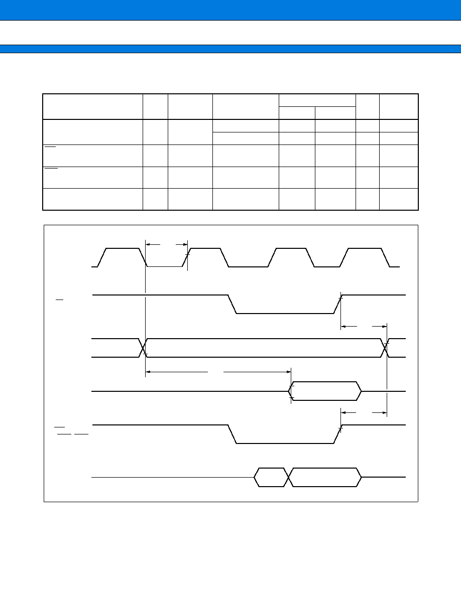
MB90610A Series
68
(14) Chip Select Output Timing
(V
CC
= +2.7 V to +5.5 V, V
SS
= 0.0 V, T
A
= ≠40∞C to +85∞C)
Parameter
Sym-
bol
Pin name
Conditions
Value
Unit
Remarks
Min.
Max.
Chip select enabled
Valid data input time
t
SVDV
CS0 to CS7
D15 to D00
V
CC
= +5.0 V±10%
--
5 t
CP
/2 ≠ 60
ns
V
CC
= +3.0 V±10%
--
5 t
CP
/2 ≠ 80
ns
RD
Chip select enabled time
t
RHSV
CS0 to CS7
RD
--
t
CP
/2 ≠ 10
--
ns
WR
Chip select enabled time
t
WHSV
CS0 to CS7
WRH, WRL
--
t
CP
/2 ≠ 10
--
ns
Enabled chip select
CLK
time
t
SVCH
CS0 to CS7
CLK
--
--
t
CP
/2 ≠ 20
ns
CLK
RD
Read data
t
SVCH
2.4 V
A23 to A00
CS0 to CS7
D15 to D00
2.4 V
2.4 V
2.4 V
0.8 V
2.4 V
0.8 V
Write data
WR
(WRL, WRH)
D15 to D00
t
RHSV
t
WHSV
t
SVDV
MB90610A Series
69
5.
A/D Converter Electrical Characteristics
(AV
CC
= V
CC
= +2.7 V to +5.5 V, AV
SS
= V
SS
= 0.0 V, 2.7 V
AVRH ≠ AVRL, T
A
= ≠40∞C to +85∞C)
*1: For V
CC
= +5.0 V±10% and a 16 MHz machine clock
*2: For V
CC
= +3.0 V±10% and a 8 MHz machine clock
*3: The current when the A/D converter is not operating or the CPU is in stop mode (for V
CC
= AV
CC
= AVRH = +5.0 V).
Notes:
∑ The relative error increases as |AVRH ≠ AVRL| decreases.
∑ The output impedance of the external circuit for the analog input should be in the following range.
Output impedance of external circuit < approx. 7 k
∑ If the output impedance of the external circuit is too high, the sampling time for the analog voltage may be too
short. (Sampling time = 3.75
µ
s @4 MHz (This corresponds to 16 MHz internal operation if the multiplier is 4.))
∑ For an external capacitor to be provided outside the chip, its capacity should desirably be thousands times
larger than that of the capacity in the chip taking in consideration the influence of the capacity distribution of
the external and internal capacitors.
Parameter
Symbol
Pin name
Value
Unit
Min.
Typ.
Max.
Resolution
--
--
--
10
10
bit
Total error
--
--
--
--
±3.0
LSB
Linearity error
--
--
--
--
±2.0
LSB
Differential linearity error
--
--
--
--
±1.5
LSB
Zero transition voltage
V
OT
AN0 to
AN7
AVRL ≠ 1.5
AVRL + 0.5
AVRL + 2.5
LSB
Full scale transition voltage
V
FST
AN0 to
AN7
AVRH ≠ 4.5 AVRH ≠ 1.5 AVRH + 0.5
LSB
Conversion time
--
--
6.125*
1
--
--
µ
s
12.25*
2
--
--
µ
s
Analog port input current
I
AIN
AN0 to
AN7
--
0.1
10
µ
A
Analog input voltage
V
AIN
AN0 to
AN7
AVRL
--
AVRH
V
Reference voltage
--
AVRH
AVRL + 2.7
--
AV
CC
V
--
AVRL
0
--
AVRH ≠ 2.7
V
Power supply current
I
A
AV
CC
--
3
--
mA
I
AH
AV
CC
--
--
5
*3
µ
A
Reference voltage supply current
I
R
AVRH
--
200
--
µ
A
I
RH
AVRH
--
--
5
*3
µ
A
Variation between channels
--
AN0 to
AN7
--
--
4
LSB
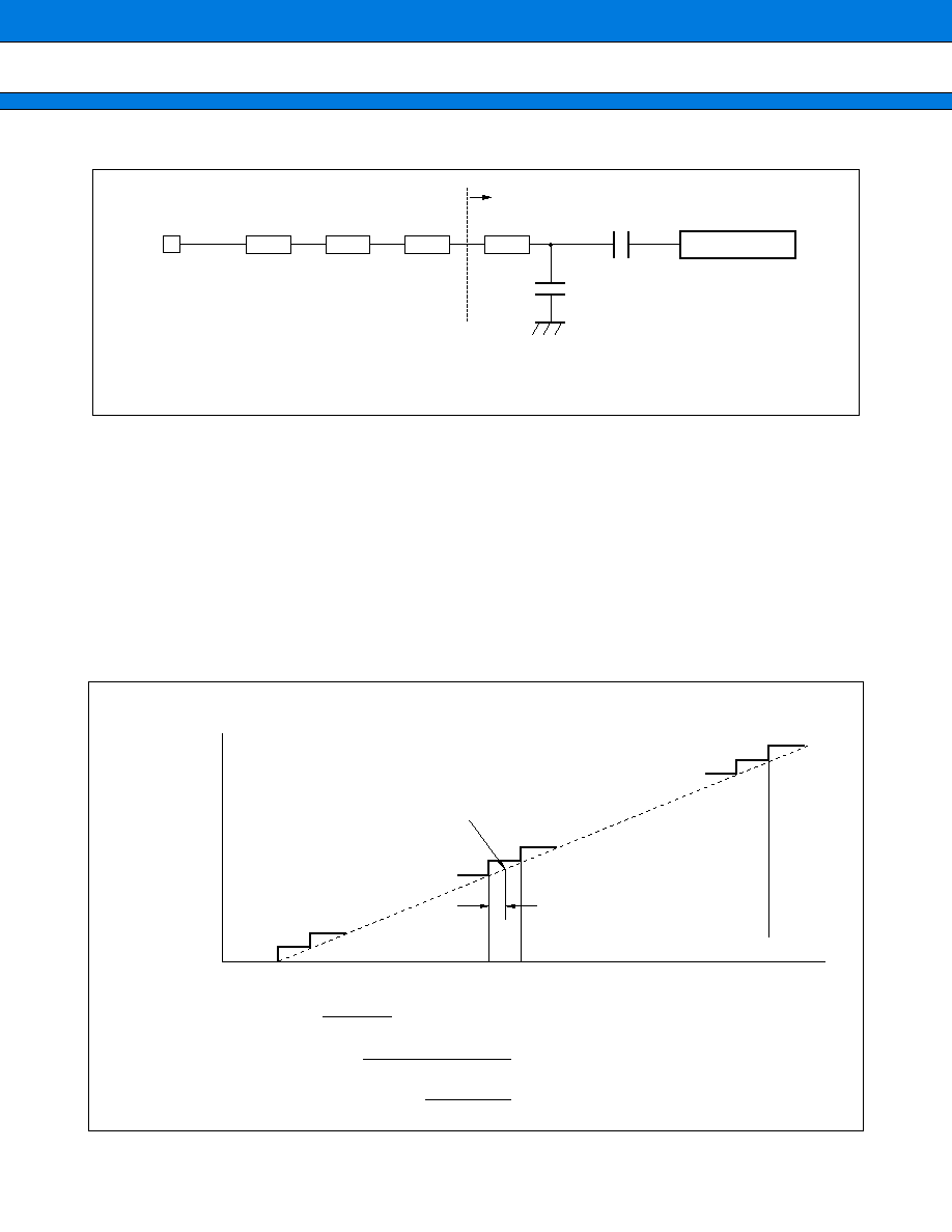
MB90610A Series
70
6.
A/D Converter Glossary
∑ Resolution
The change in analog voltage that can be recognized by the A/D converter.
If the resolution is 10 bits, the analog voltage can be resolved into 2
10
= 1024 steps.
∑ Total error
The deviation between the actual and logic value attributable to offset error, gain error, non-linearity error, and
noise.
∑ Linearity error
The deviation between the actual conversion characteristic of the device and the line linking the zero transition
point (00 0000 0000
00 0000 0001) and the full scale transition point (11 1111 1110
11 1111 1111).
∑ Differential linearity error
The variation from the ideal input voltage required to change the output code by 1 LSB.
Comparator
Analog input
R
ON1
R
ON2
C
1
C
0
R
ON1
=
1.5 k
(approx.) (V
CC
= 5.0 V)
R
ON2
=
0.5 k
(approx.) (V
CC
= 5.0 V)
R
ON3
=
0.5 k
(approx.) (V
CC
= 5.0 V)
R
ON4
=
0.5 k
(approx.) (V
CC
= 5.0 V)
C
0
=
60 pF (approx.)
C
1
=
4 pF (approx.)
R
ON3
R
ON4
Sample and hold circuit
Note: The above values are for reference only.
∑ Model of The Analog Input Circuit
Digital output
1111 1111
1111 1110
0000 0001
0000 0000
0000 0010
∑
∑
∑
∑
∑
∑
∑
∑
∑
∑
∑
V
OT
V
NT
V
(N + 1)T
V
FST
(1 LSB
◊
N + V
OT
)
Analog input
Linearity error
1 LSB =
1022
V
FST
≠ V
OT
Linearity error =
1 LSB
V
NT
≠ (1 LSB
◊
N + V
OT
)
(LSB)
11
11
00
00
00
1 LSB
V
(N + 1)T
≠ V
NT
≠ 1 (LSB)
Differential linearity error =
MB90610A Series
71
s
s
s
s
EXAMPLES CHARACTERISTICS
V
CC
= 5.0 V
V
CC
= 4.5 V
I
OH
(mA)
≠8
1.0
0.9
0.8
0.7
0.6
0.5
0.4
0.3
0.2
0.1
0.0
V
OH
≠ I
OH
≠4
≠6
≠2
V
CC
= 4.0 V
V
CC
= 3.0 V
V
CC
= 2.7 V
V
CC
= 3.5 V
T
A
= +25∞C
V
OH
(V)
V
CC
= 5.0 V
V
OL
(V)
V
CC
= 4.5 V
I
OL
(mA)
8
1.0
0.9
0.8
0.7
0.6
0.5
0.4
0.3
0.2
0.1
0.0
V
OL
≠ I
OL
4
6
2
V
CC
= 4.0 V
V
CC
= 3.0 V
V
CC
= 2.7 V
V
CC
= 3.5 V
T
A
= +25∞C
5.0
4.5
4.0
3.5
3.0
2.5
2.0
1.5
1.0
0.5
0
V
IN
(V)
V
CC
(V)
2
3
4
5
6
T
A
= +25∞C
V
IN
≠ V
CC
(CMOS Input)
5.0
4.5
4.0
3.5
3.0
2.5
2.0
1.5
1.0
0.5
0
V
IN
(V)
V
CC
(V)
2
3
4
5
6
T
A
= +25∞C
V
IN
≠ V
CC
(Hysteresis Input)
V
IHS
V
ILS
(3) "H" Level Input Voltage/"L" Level Input Voltage
(4) "H" Level Input Voltage/"L" Level Input Voltage
(1) "H" Level Output Voltage
(2) "L" Level Output Voltage
V
IHS
: Threshold when input voltage in hysteresis
characteristics is set to "H" level
V
ILS
: Threshold when input voltage in hysteresis
characteristics is set to "L" level
MB90610A Series
72
(5) Power Supply Current (fcp = internal frequency)
(6) Pull-up Resistance
I
CC
(mA)
I
CC
≠ V
CC
70
65
60
55
50
45
40
35
30
25
20
15
10
5
0
3.0
4.0
5.0
6.0
V
CC
(V)
f
cp
= 16 MHz
f
cp
= 12.5 MHz
f
cp
= 8 MHz
f
cp
= 4 MHz
T
A
= +25∞C
I
CCS
(mA)
I
CCS
≠ V
CC
15
14
13
12
11
10
9
8
7
6
5
4
3
2
1
0
3.0
4.0
5.0
6.0
V
CC
(V)
f
cp
= 16 MHz
f
cp
= 12.5 MHz
f
cp
= 8 MHz
f
cp
= 4 MHz
T
A
= +25∞C
I
A
(mA)
I
A
≠ AV
CC
3.0
4.0
5.0
6.0
AV
CC
(V)
6.0
5.5
5.0
4.5
4.0
3.5
3.0
2.5
2.0
1.5
1.0
0.5
0
T
A
= +25∞C
f
CP
= 16 MHz
I
R
(mA)
I
R
≠ AVR
3.0
4.0
5.0
6.0
AVR (V)
0.30
0.20
0.10
0
T
A
= +25∞C
f
CP
= 16 MHz
3.0
3.5
4.0
4.5
5.0
5.5
6.0
1000
R (k )
V
CC
(V)
100
10
2.5
T
A
= +25∞C
R ≠ V
CC
MB90610A Series
73
s
s
s
s
ORDERING INFORMATION
Part number
Package
Remarks
MB90611APFV
100-pin Plastic LQFP
(FPT-100P-M05)
MB90611APF
100-pin Plastic QFP
(FPT-100P-M06)
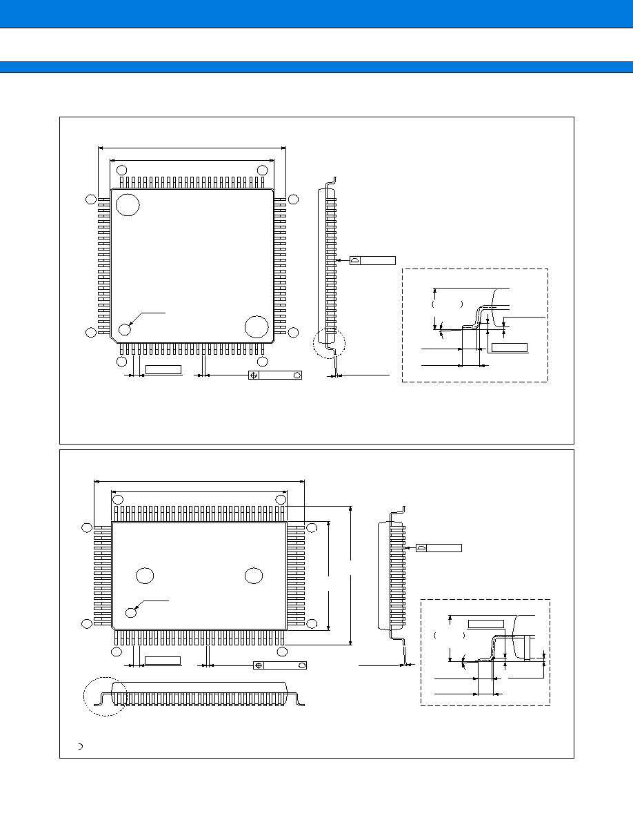
MB90610A Series
74
s
s
s
s
PACKAGE DIMENSIONS
C
2001 FUJITSU LIMITED F100008S-c-4-4
1
30
31
50
51
80
81
100
20.00±0.20(.787±.008)
23.90±0.40(.941±.016)
14.00±0.20
(.551±.008)
17.90±0.40
(.705±.016)
INDEX
0.65(.026)
0.32±0.05
(.013±.002)
M
0.13(.005)
"A"
0.17±0.06
(.007±.002)
0.10(.004)
Details of "A" part
0~8∞
(.035±.006)
0.88±0.15
(.031±.008)
0.80±0.20
0.25(.010)
3.00
+0.35
≠0.20
+.014
≠.008
.118
(Mounting height)
0.25±0.20
(.010±.008)
(Stand off)
2000 FUJITSU LIMITED F100007S-3c-5
14.00±0.10(.551±.004)SQ
16.00±0.20(.630±.008)SQ
1
25
26
51
76
50
75
100
0.50(.020)
0.20±0.05
(.008±.002)
M
0.08(.003)
0.145±0.055
(.0057±.0022)
0.08(.003)
"A"
INDEX
.059
≠.004
+.008
≠0.10
+0.20
1.50
(Mounting height)
0∞~8∞
0.50±0.20
(.020±.008)
0.60±0.15
(.024±.006)
0.25(.010)
0.10±0.10
(.004±.004)
Details of "A" part
(Stand off)
Dimensions in mm (inches)
Dimensions in mm (inches)
100-pin Plastic QFP
100-pin Plastic LQFP
(FPT-100P-M05)
(FPT-100P-M06)

MB90610A Series
FUJITSU LIMITED
All Rights Reserved.
The contents of this document are subject to change without notice.
Customers are advised to consult with FUJITSU sales
representatives before ordering.
The information and circuit diagrams in this document are
presented as examples of semiconductor device applications, and
are not intended to be incorporated in devices for actual use. Also,
FUJITSU is unable to assume responsibility for infringement of
any patent rights or other rights of third parties arising from the use
of this information or circuit diagrams.
The products described in this document are designed, developed
and manufactured as contemplated for general use, including
without limitation, ordinary industrial use, general office use,
personal use, and household use, but are not designed, developed
and manufactured as contemplated (1) for use accompanying fatal
risks or dangers that, unless extremely high safety is secured, could
have a serious effect to the public, and could lead directly to death,
personal injury, severe physical damage or other loss (i.e., nuclear
reaction control in nuclear facility, aircraft flight control, air traffic
control, mass transport control, medical life support system, missile
launch control in weapon system), or (2) for use requiring
extremely high reliability (i.e., submersible repeater and artificial
satellite).
Please note that Fujitsu will not be liable against you and/or any
third party for any claims or damages arising in connection with
above-mentioned uses of the products.
Any semiconductor devices have an inherent chance of failure. You
must protect against injury, damage or loss from such failures by
incorporating safety design measures into your facility and
equipment such as redundancy, fire protection, and prevention of
over-current levels and other abnormal operating conditions.
If any products described in this document represent goods or
technologies subject to certain restrictions on export under the
Foreign Exchange and Foreign Trade Law of Japan, the prior
authorization by Japanese government will be required for export
of those products from Japan.
F0109
©
FUJITSU LIMITED Printed in Japan