DS07-16302-2E
FUJITSU SEMICONDUCTOR
DATA SHEET
32-bit RISC Microcontroller
CMOS
FR Family MB91106
MB91106
s
DESCRIPTION
The MB91106 is a standard single-chip microcontroller constructed around the 32-bit RISC CPU (FR* family)
core with abundant I/O resources and bus control functions optimized for high-performance/high-speed CPU
processing for embedded controller applications. To carry out hi-speed performance of CPU instructions,
instruction/data ROM of 64 Kbytes and RAM of 2 Kbytes are embedded in the MB91106.
The MB91101 is optimized for applications requiring high-performance CPU processing such as navigation
systems, high-performance FAXs and printer controllers.
*: FR Family stands for FUJITSU RISC controller.
s
FEATURES
FR CPU
∑ 32-bit RISC, load/store architecture, 5-stage pipeline
∑ Operating clock frequency: Internal 50 MHz/external 25 MHz (PLL used at source oscillation 12.5 MHz)
∑ General purpose registers: 32 bits
◊
16
∑ 16-bit fixed length instructions (basic instructions), 1 instruction/1 cycle
∑ Memory to memory transfer, bit processing, barrel shifter processing: Optimized for embedded applications
∑ Function entrance/exit instructions, multiple load/store instructions of register contents, instruction systems
supporting high level languages
∑ Register interlock functions, efficient assembly language coding
∑ Branch instructions with delay slots: Reduced overhead time in branch executions
(Continued)
s
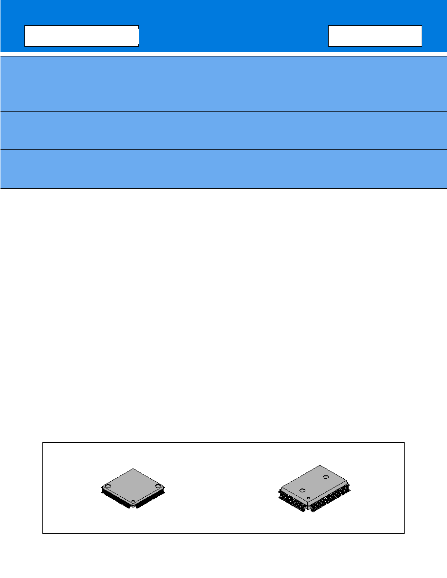
PACKAGE
100-pin Plastic LQFP
(FPT-100P-M05)
100-pin Plastic QFP
(FPT-100P-M06)

MB91106 Series
2
(Continued)
∑ Internal multiplier/supported at instruction level
Signed 32-bit multiplication: 5 cycles
Signed 16-bit multiplication: 3 cycles
∑ Interrupt (push PC and PS): 6 cycles, 16 priority levels
External bus interface
∑ Clock doublure: Maximum internal bus 50 MHz, maximum external bus 25 MHz operation
∑ 25-bit address bus (32 Mbytes memory space)
∑ 8/16-bit data bus
∑ Basic external bus cycle: 2 clock cycles
∑ Chip select outputs for setting down to a minimum memory block size of 64 Kbytes: 6
∑ Interface supported for various memory technologies
DRAM interface (area 4 and 5)
∑ Automatic wait cycle insertion: Flexible setting, from 0 to 7 for each area
∑ Unused data/address pins can be configured us input/output ports
∑ Little endian mode supported (Select 1 area from area 1 to 5)
DRAM interface
∑ 2 banks independent control (area 4 and 5)
∑ Normal mode (double CAS DRAM)/high-speed page mode (single CAS DRAM)/Hyper DRAM
∑ Basic bus cycle: Normally 5 cycles, 2-cycle access possible in high-speed page mode
∑ Programmable waveform: Automatic 1-cycle wait insertion to RAS and CAS cycles
∑ DRAM refresh
CBR refresh (interval time configurable by 6-bit timer)
Self-refresh mode
∑ Supports 8/9/10/12-bit column address width
∑ 2CAS/1WE, 2WE/1CAS selective
DMA controller (DMAC)
∑ 8 channels
∑ Transfer incident/external pins/internal resource interrupt requests
∑ Transfer sequence: Step transfer/block transfer/burst transfer/continuous transfer
∑ Transfer data length: 8 bits/16 bits/32 bits selective
∑ NMI/interrupt request enables temporary stop operation
UART
∑ 3 independent channels
∑ Full-duplex double buffer
∑ Data length: 7 bits to 9 bits (non-parity), 6 bits to 8 bits (parity)
∑ Asynchronous (start-stop system), CLK-synchronized communication selective
∑ Multi-processor mode
∑ Internal 16-bit timer (U-TIMER) operating as a proprietary baud rate generator: Generates any given baud rate
∑ Use external clock can be used as a transfer clock
∑ Error detection: Parity, frame, overrun
3
MB91106 Series
(Continued)
10-bit A/D converter (successive approximation conversion type)
∑ 10-bit resolution, 4 channels
∑ Successive approximation type: Conversion time of 5.6
µ
s at 25 MHz
∑ Internal sample and hold circuit
∑ Conversion mode: Single conversion/scanning conversion/repeated conversion/stop conversion selective
∑ Start: Software/external trigger/internal timer selective
16-bit reload timer
∑ 3 channels
∑ Internal clock: 2 clock cycle resolution, divide by 2/8/32 selective
Other interval timers
∑ 16-bit timer: 3 channels (U-TIMER)
∑ PWM timer: 4 channels
∑ Watchdog timer: 1 channel
Bit search module
First bit transition "1" or "0" from MSB can be detected in 1 cycle
Interrupt controller
∑ External interrupt input: Non-maskable interrupt (NMI), normal interrupt
◊
4 (INT0 to INT3)
∑ Internal interrupt incident: UART, DMA controller (DMAC), 10-bit A/D converter, 16-bit reload-timer, PWM timer,
U-TIMER and delayed interrupt module
∑ Priority levels of interrupts are programmable except for non-maskable interrupt (in 16 steps)
Others
∑ Reset cause: Power-on reset/software reset/external reset
∑ Low-power consumption mode: Sleep mode/stop mode
∑ Clock control
Gear function: Operating clocks for CPU and peripherals are independently selective
Gear clock can be selected from 1/1, 1/2, 1/4 and 1/8 (or 1/2, 1/4, 1/8 and 1/16)
(However, operating frequency for peripherals is less than 25 MHz.)
∑ Packages: LQFP-100 and QFP-100
∑ CMOS technology (0.35
µ
m)
∑ Power supply voltage: 3.3 V
±
0.3 V
s
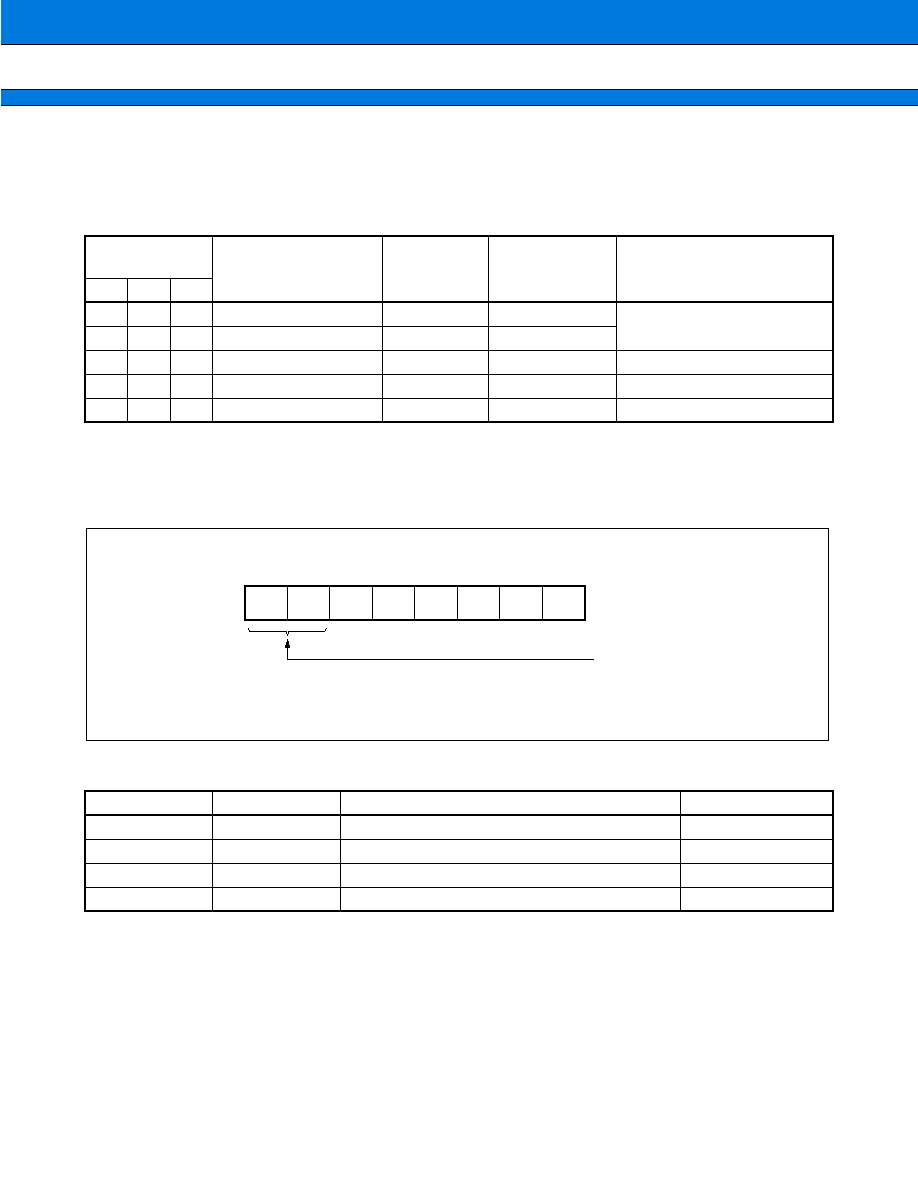
PRODUCT LINEUP
MB91V106
Classification
Mass production products
(mask ROM products)
Piggyback/evaluation product
(for evaluation and development)
IROM size
63 Kbytes
--
IRAM size
--
64 Kbytes
CROM size
64 Kbytes
--
CRAM size
--
64 Kbytes
RAM size
2 Kbytes
5 Kbytes
I $
--
Other
Under trial manufacture
Under development
MB91106
Part number
Parameter
MB91106 Series
4
s
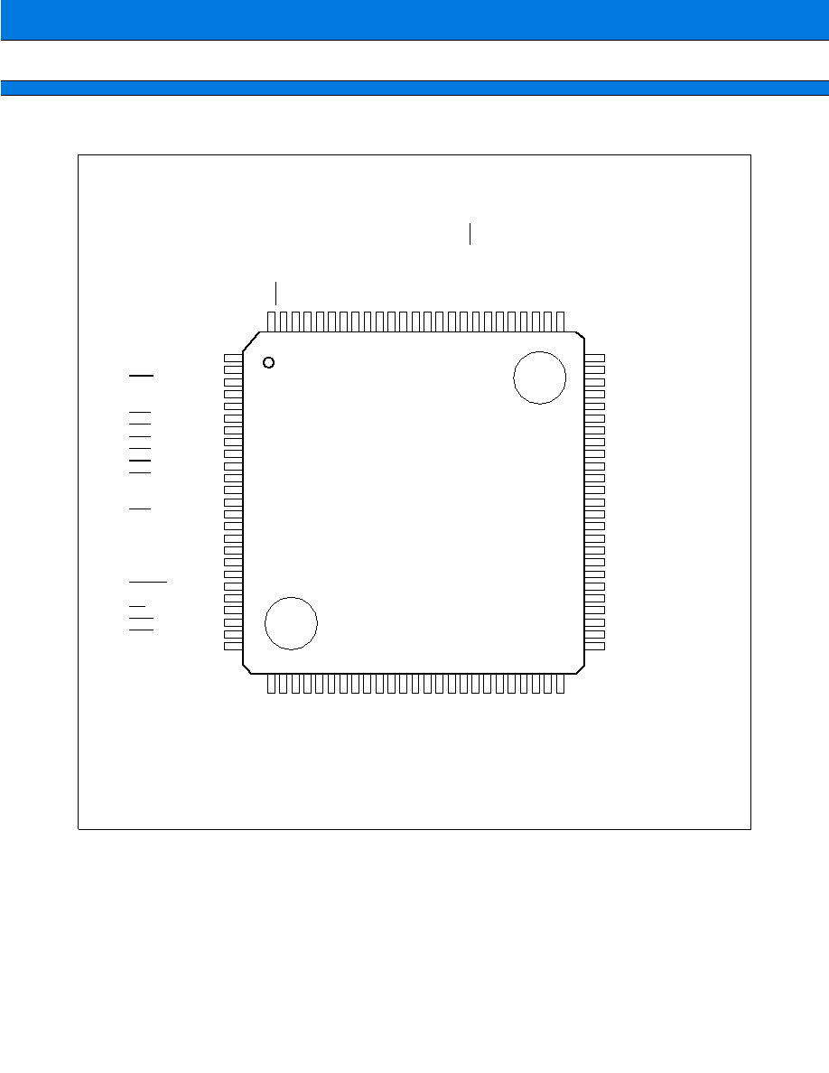
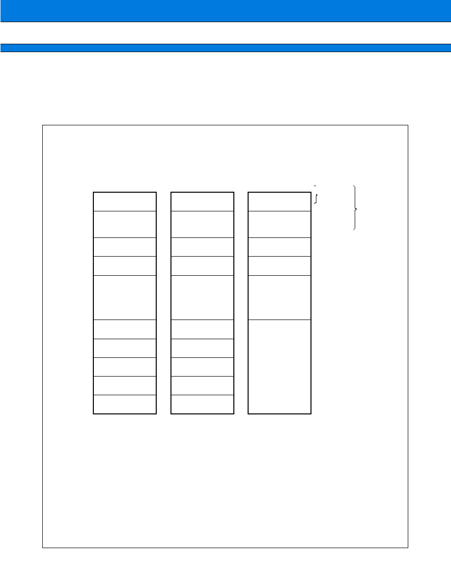
PIN ASSIGNMENT
1
2
3
4
5
6
7
8
9
10
11
12
13
14
15
16
17
18
19
20
21
22
23
24
25
75
74
73
72
71
70
69
68
67
66
65
64
63
62
61
60
59
58
57
56
55
54
53
52
51
26
27
28
29
30
31
32
33
34
35
36
37
38
39
40
41
42
43
44
45
46
47
48
49
50
100
99
98
97
96
95
94
93
92
91
90
89
88
87
86
85
84
83
82
81
80
79
78
77
76
CS1L/PB5/DREQ2
CS1H/PB6/DACK2
DW1/PB7
V
CC
CLK/PA6
CS5/PA5
CS4/PA4
CS3/PA3/EOP1
CS2/PA2
CS1/PA1
CS0/PA0
NMI
V
CC
RST
V
SS
MD0
MD1
MD2
RDY/P80
BGRNT/P81
BRQ/P82
RD/P83
WR0/P84
WR1/P85
D16/P20
AN3
AN2
AN1
AN0
AV
SS
/AVRL
AVRH
AV
CC
A24/EOP0/P70
A23/P67
A22/P66
V
SS
A21/P65
A20/P64
A19/P63
A18/P62
A17/P61
A16/P60
A15/P57
A14/P56
A13/P55
A12/P54
A11/P53
A10/P52
A09/P51
A08/P50
RAS1/PB4/EOP2
DW
0
/PB3
CS0H/PB2
CS0L/PB1
RAS0/PB0
INT0/PE0
INT1/PE1
V
CC
X0
X1
V
SS
INT2/SC1/PE2
INT3/SC2/PE3
DREQ0/PE4
DREQ1/PE5
DA
C
K
0
/
P
E
6
DA
C
K
1
/
P
E
7
OCP
A
0/PF7/A
T
G
SO
2/OC
P
A
2
/
PF6
SI2/OCP
A
1/PF5
SO1/TRG3/PF4
SI1/TRG2/PF3
SC
0/O
C
P
A
3
/
PF2
SO0/TRG1/PF1
SI0/TRG0/PF0
D17/P21
D18/P22
D19/P23
D20/P24
D21/P25
D22/P26
D23/P27
D24/P30
D25/P31
D26/P32
D27/P33
D28/P34
D29/P35
D30/P36
V
SS
D31/P37
A00/P40
V
CC
A01/P41
A02/P42
A03/P43
A04/P44
A05/P45
A06/P46
A07/P47
(Top view)
(FPT-100P-M05)
5
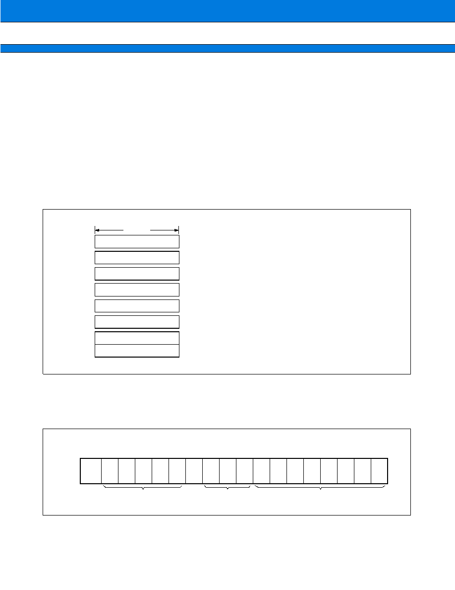
MB91106 Series
1
2
3
4
5
6
7
8
9
10
11
12
13
14
15
16
17
18
19
20
21
22
23
24
25
26
27
28
29
30
(Top view)
(FPT-100P-M06)
80
79
78
77
76
75
74
73
72
71
70
69
68
67
66
65
64
63
62
61
60
59
58
57
56
55
54
53
52
51
31
32
33
34
35
36
37
38
39
34
41
42
43
44
45
46
47
48
49
50
100
99
98
97
96
95
94
93
92
91
90
89
88
87
86
85
84
83
82
81
CS0H/PB2
DW0/PB3
RAS1/PB4/EOP2
CS1L/PB5/DREQ2
CS1H/PB6/DACK2
DW1/PB7
V
CC
CLK/PA6
CS5/PA5
CS4/PA4
CS3/PA3/EOP1
CS2/PA2
CS1/PA1
CS0/PA0
NMI
V
CC
RST
V
SS
MD0
MD1
MD2
RDY/P80
BGRNT/P81
BRQ/P82
RD/P83
WR0/P84
WR1/P85
D16/P20
D17/P21
D18/P22
SO0/TRG1/PF1
SI0/TRG0/PF0
AN3
AN2
AN1
AN0
AV
SS
/AVRL
AVRH
AV
CC
A24/EOP0/P70
A23/P67
A22/P66
V
SS
A21/P65
A20/P64
A19/P63
A18/P62
A17/P61
A16/P60
A15/P57
A14/P56
A13/P55
A12/P54
A11/P53
A10/P52
A09/P51
A08/P50
A07/P47
A06/P46
A05/P45
CS0L/PB1
RAS0/PB0
INT0/PE0
INT1/PE1
V
CC
X0
X1
V
SS
INT2/SC1/PE2
INT3/SC2/PE3
DREQ0/PE4
DREQ1/PE5
DA
C
K
0
/
P
E
6
DA
C
K
1
/
P
E
7
OCP
A
0/PF7/A
T
G
SO
2/OC
P
A
2
/
PF6
SI2/OCP
A
1/PF5
SO1/TRG3/PF4
SI1/TRG2/PF3
SC
0/O
C
P
A
3
/
PF2
D19/P23
D20/P24
D21/P25
D22/P26
D23/P27
D24/P30
D25/P31
D26/P32
D27/P33
D28/P34
D29/P35
D30/P36
V
SS
D31/P37
A00/P40
V
CC
A01/P41
A02/P42
A03/P43
A04/P44
MB91106 Series
6
s
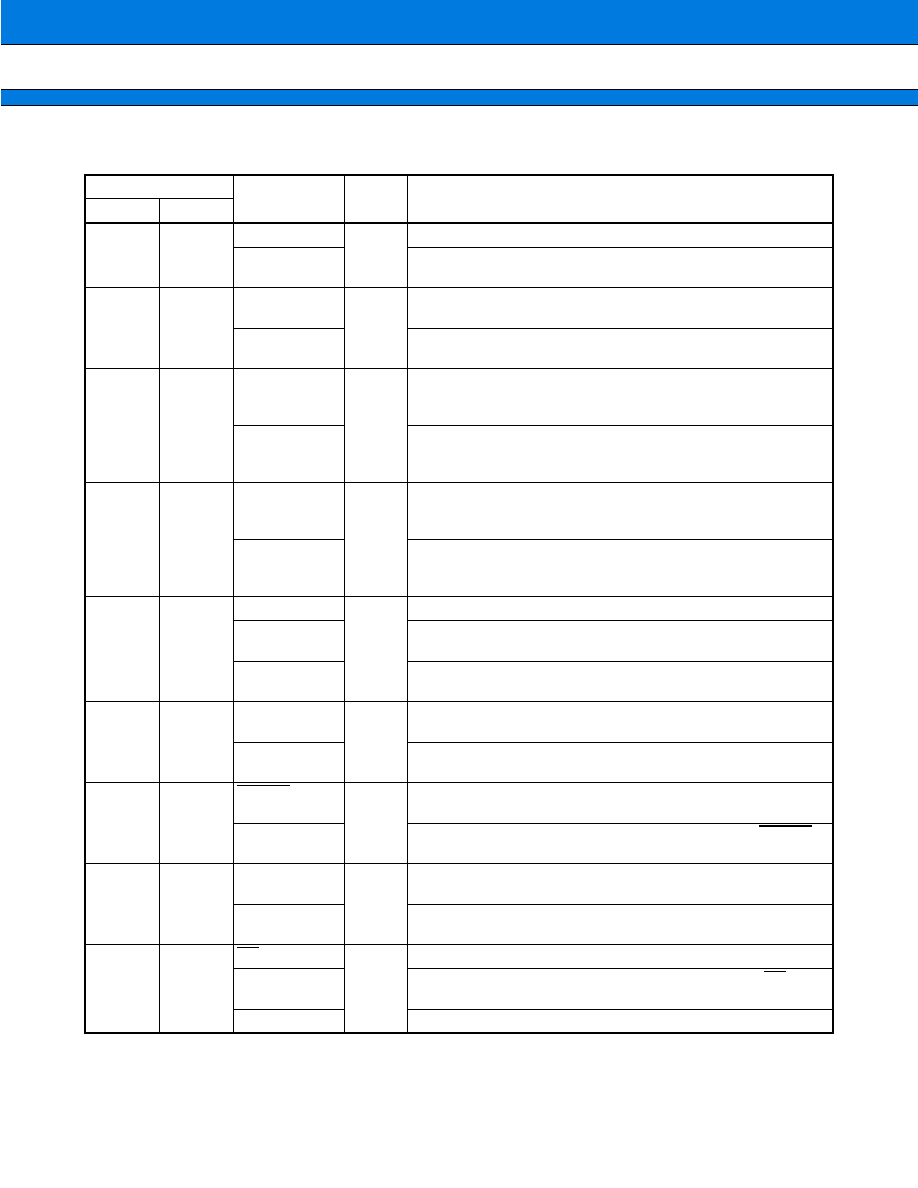
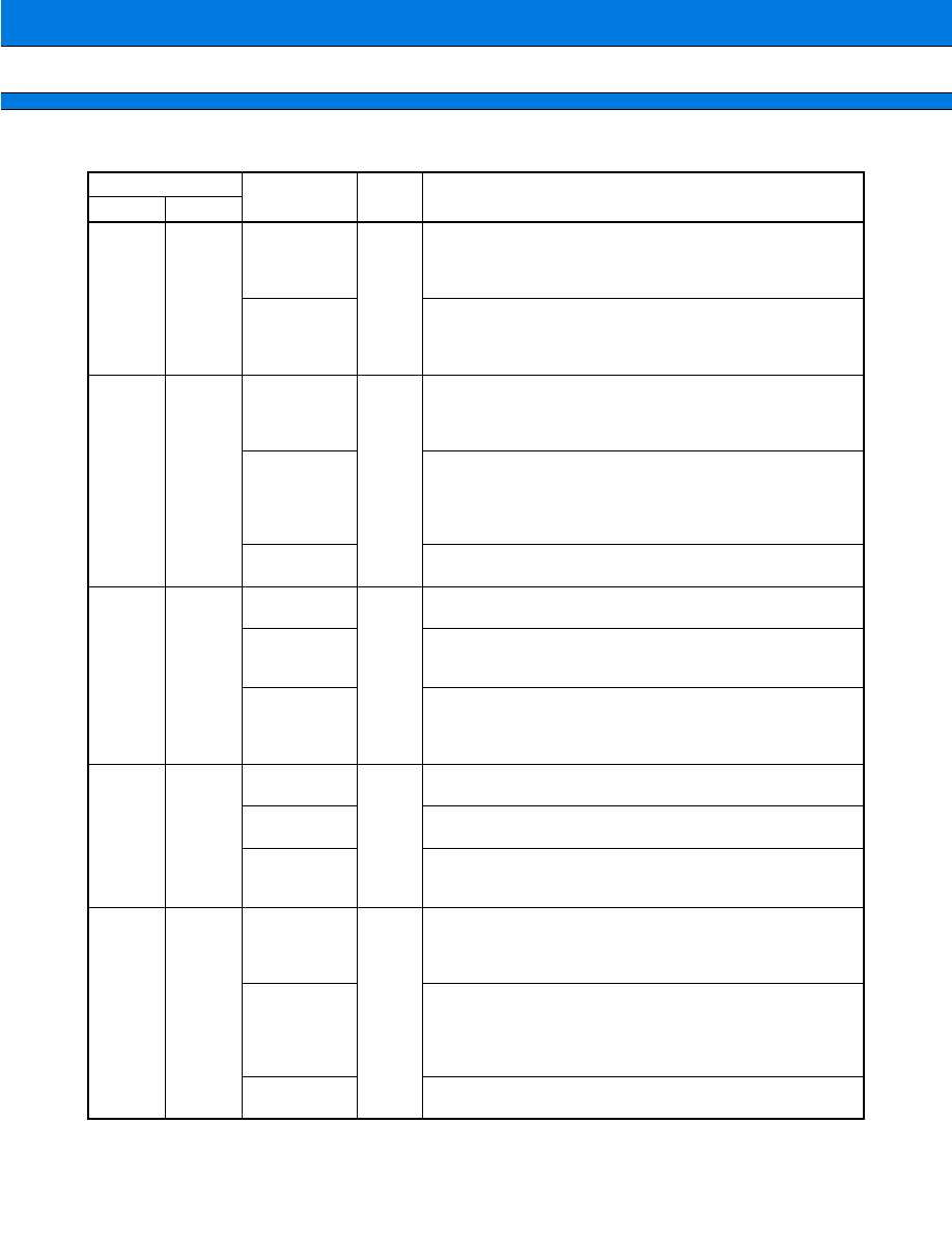
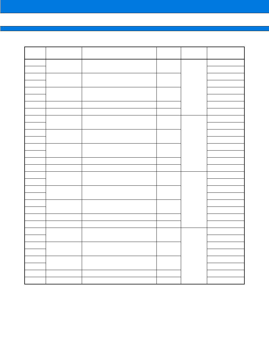
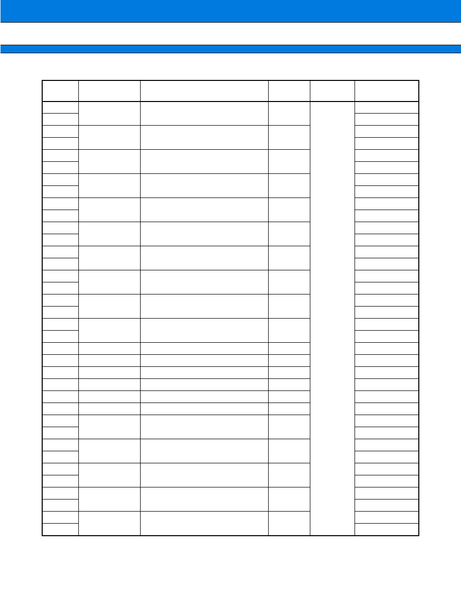
PIN DESCRIPTION
*1: FPT-100P-M05
(Continued)
*2: FPT-100P-M06
Pin no.
Pin name
Circuit
type
Function
LQFP*
1
QFP*
2
25 to 32
28 to 35 D16 to D23
C
Bit 16 to bit 23 of external data bus
P20 to P27
Can be configured as general purpose I/O port when external
data bus width is set to 8-bit or in single chip mode.
33 to 39,
41
36 to 42,
44
D24 to D30,
D31
C
Bit 24 to bit 31 of external data bus
P30 to P36,
P37
Can be configured as general purpose I/O ports when not used
as address bus.
42,
44 to 50,
51 to 58
45,
47 to 53,
54 to 61
A00,
A01 to A07,
A08 to A15
E
Bit 00 to bit 15 of external address bus
P40,
P41 to P47,
P50 to P57
Can be configured as general purpose I/O ports when not used
as address bus.
59 to 64,
66,
67
62 to 67,
69,
70
A16 to A21,
A22,
A23
E
Bit 16 to bit 23 of external address bus
P60 to P67,
P69,
P70
Can be configured as general purpose I/O ports when not used
as address bus.
68
71
A24
E
Bit 24 of external address bus
EOP0
Can be configured as DMAC EOP output (ch. 0) when DMAC
EOP output is enabled.
P70
Can be configured as general purpose I/O port when A24 and
EOP0 are not used.
19
22
RDY
C
External ready input
Inputs "0" when bus cycle is being executed and not completed.
P80
Can be configured as general purpose I/O port when RDY is
not used.
20
23
BGRNT
E
External bus release acknowledge output
Outputs "L" level when external bus is released.
P81
Can be configured as general purpose I/O port when BGRNT is
not used.
21
24
BRQ
C
External bus release request input
Inputs "1" when release of external bus is required.
P82
Can be configured as general purpose I/O port when BRQ is
not used.
22
25
RD
E
Read strobe output pin for external bus
P83
Can be configured as general purpose I/O port when RD is not
used.
7
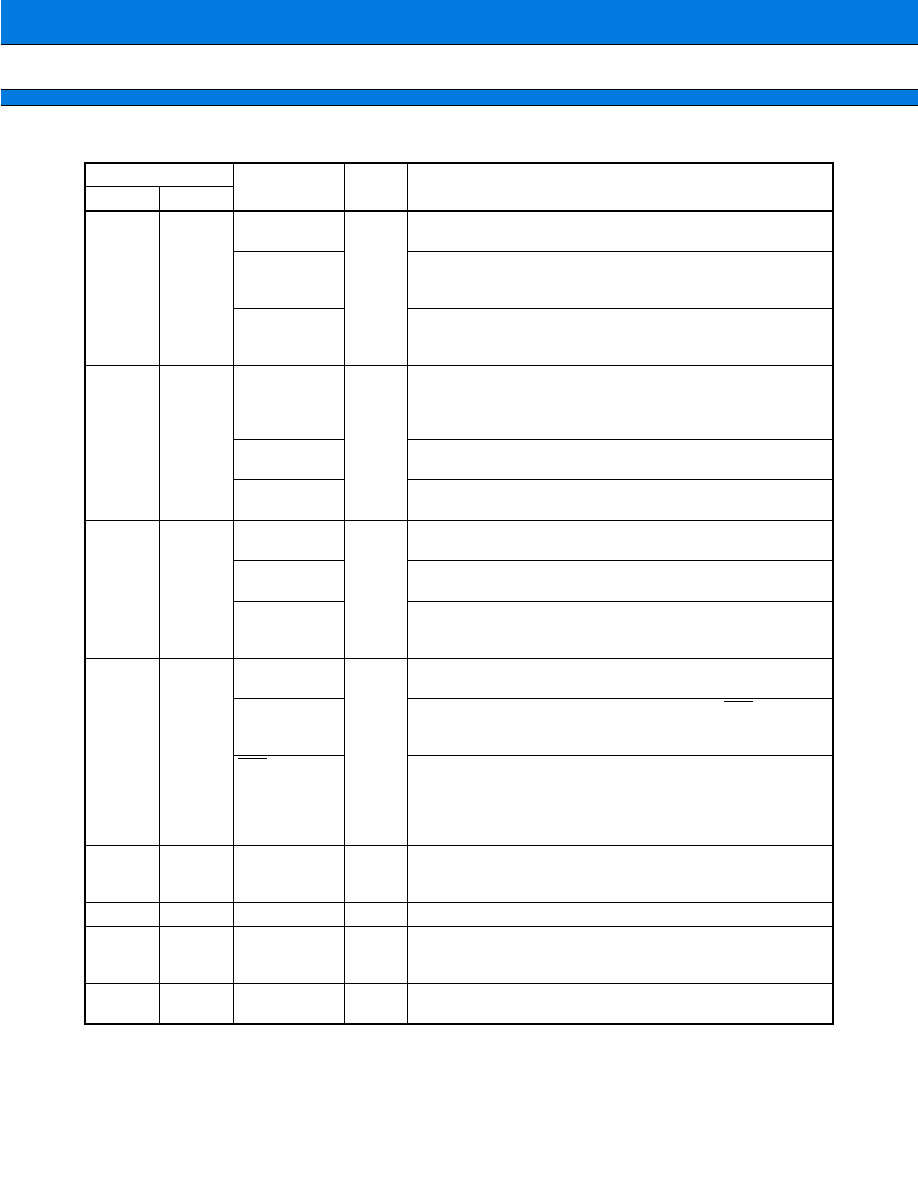
MB91106 Series
*1: FPT-100P-M05
(Continued)
*2: FPT-100P-M06
Pin no.
Pin name
Circuit
type
Function
LQFP*
1
QFP*
2
23
26
P84
E
Can be configured as general purpose I/O port when WR0 is
not used.
WR0
Write strobe output pin for external bus
Relation between control signals and effective byte locations is
as follows:
Note: WR1 is Hi-Z during resetting.
Attach an external pull-up resister when using at 16-bit
bus width.
24
27
WR1
E
P85
Can be configured as general purpose I/O port when WR1 is
not used.
11
14
CS0
E
Chip select 0 output ("L" active)
PA0
Can be configured as general purpose I/O port when CS0 is
not used.
10
13
CS1
E
Chip select 1 output ("L" active)
PA1
Can be configured as general purpose I/O port when CS1 is
not used.
9
12
CS2
E
Chip select 2 output ("L" active)
PA2
Can be configured as a port when CS2 is not used.
8
11
CS3
E
Chip select 3 output ("L" active)
PA3
Can be configured as a port when CS3 and EOP1 are not
used.
EOP1
EOP output pin for DMAC (ch. 1)
This function is available when EOP output for DMAC is
enabled.
7
10
CS4
E
Chip select 4 output ("L" active)
PA4
Can be configured as general purpose I/O port when CS4 is
not used.
6
9
CS5
E
Chip select 5 output ("L" active)
PA5
Can be configured as general purpose I/O port when CS5 is
not used.
5
8
CLK
E
System clock output
Outputs clock signal of external bus operating frequency.
PA6
Can be configured as general purpose I/O port when CLK is
not used.
16-bit
bus width
8-bit
bus width
Single chip
mode
D31 to D24
WR0
WR0
(I/O port
enabled)
D23 to D16
WR1
(I/O port
enabled)
(I/O port
enabled)
MB91106 Series
8
*1: FPT-100P-M05
(Continued)
*2: FPT-100P-M06
Pin no.
Pin name
Circuit
type
Function
LQFP*
1
QFP*
2
96
99
RAS0
E
RAS output for DRAM bank 0
PB0
Can be configured as general purpose I/O port when RAS0 is
not used.
97
100
CS0L
E
CASL output for DRAM bank 0
PB1
Can be configured as general purpose I/O port when CS0L is
not used.
98
1
CS0H
E
CASH output for DRAM bank 0
PB2
Can be configured as general purpose I/O port when CS0H is
not used.
99
2
DW0
E
WE output for DRAM bank 0 ("L" active)
PB3
Can be configured as general purpose I/O port when DW0 is
not used.
100
3
RAS1
E
RAS output for DRAM bank 1
PB4
Can be configured as general purpose I/O port when RAS1
and EOP2 are not used.
EOP2
DMAC EOP output (ch. 2)
This function is available when DMAC EOP output is enabled.
1
4
CS1L
E
CASL output for DRAM bank 1
PB5
Can be configured as general purpose I/O port when CS1L
and DREQ are not used.
DREQ2
External transfer request input pin for DMA
This pin is used for input when external trigger is selected to
cause DMAC operation, and it is necessary to disable output
for other functions from this pin unless such output is made
intentionally.
2
5
CS1H
E
CASH output for DRAM bank 1
PB6
Can be configured as general purpose I/O port when CS1H
and DACK2 are not used.
DACK2
External transfer request accept output pin for DMAC (ch. 2)
This function is available when transfer request output for
DMAC is enabled.
3
6
DW1
E
WE output for DRAM bank 1 ("L" active)
PB7
Can be configured as general purpose I/O port when DW1 is
not used.
16 to 18
19 to 21
MD0 to MD2
F
Mode pins 0 to 2
MCU basic operation mode is set by these pins.
Directly connect these pins with V
CC
or V
SS
for use.
92
95
X0
A
Clock (oscillator) input
91
94
X1
A
Clock (oscillator) output
14
17
RST
B
External reset input
12
15
NMI
G
NMI (non-maskable interrupt pin) input ("L" active)
9
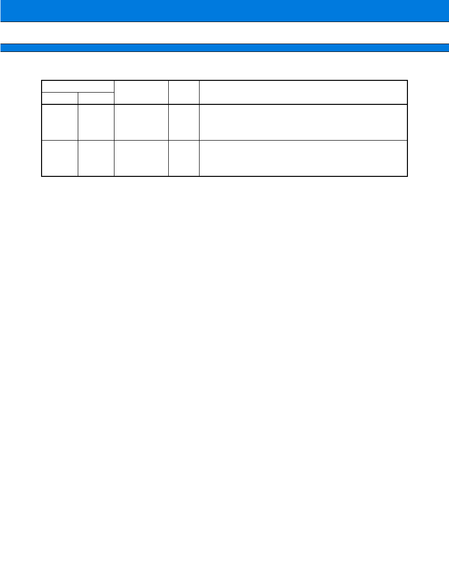
MB91106 Series
*1: FPT-100P-M05
(Continued)
*2: FPT-100P-M06
Pin no.
Pin name
Circuit
type
Function
LQFP*
1
QFP*
2
95,
94
98,
97
INT0,
INT1
E
External interrupt request input pins
These pins are used for input during corresponding interrupt is
enabled, and it is necessary to disable output for other
functions from these pins unless such output is made
intentionally.
PE0,
PE1
Can be configured as general purpose I/O ports when INT0
and INT1 are not used.
89
92
INT2
E
External interrupt request input pin
This pin is used for input during corresponding interrupt is
enabled, and it is necessary to disable output for other
functions from this pin unless such output is made intentionally.
SC1
Clock I/O pin for UART1
Clock output is available when clock output of UART1 is
enabled.
PE2
Can be configured as general purpose I/O port when INT2 and
SC1 are not used.
This function is available when UART1 clock output is disabled.
88
91
INT3
E
External interrupt request input pin
This pin is used for input during corresponding interrupt is
enabled, and it is necessary to disable output for other
functions from this pin unless such output is made intentionally.
SC2
UART2 clock I/O pin
Clock output is available when UART2 clock output is enabled.
PE3
Can be configured as general purpose I/O port when INT3 and
SC2 are not used.
This function is available when UART2 clock output is disabled.
87,
86
90,
89
DREQ0,
DREQ1
E
External transfer request input pins for DMA
These pins are used for input when external trigger is selected
to cause DMAC operation, and it is necessary to disable output
for other functions from these pins unless such output is made
intentionally.
PE4,
PE5
Can be configured as general purpose I/O ports when DREQ0
and DREQ1 are not used.
85
88
DACK0
E
External transfer request acknowledge output pin for DMAC
(ch. 0)
This function is available when transfer request output for
DMAC is enabled.
PE6
Can be configured as general purpose I/O port when DACK0 is
not used.
This function is available when transfer request acknowledge
output for DMAC or DACK0 output is disabled.
MB91106 Series
10
*1: FPT-100P-M05
(Continued)
*2: FPT-100P-M06
Pin no.
Pin name
Circuit
type
Function
LQFP*
1
QFP*
2
84
87
DACK1
E
External transfer request acknowledge output pin for DMAC
(ch. 1)
This function is available when transfer request output for
DMAC is enabled.
PE7
Can be configured as general purpose I/O port when DACK1 is
not used.
This function is available when transfer request output for
DMAC or DACK1 output is disabled.
76
79
SI0
E
UART0 data input pin
This pin is used for input during UART0 is in input operation,
and it is necessary to disable output for other functions from
this pin unless such output is made intentionally.
TRG0
PWM timer external trigger input pin (ch.0)
This pin is used for input during PWM timer external trigger is
in input operation, and it is necessary to disable output for
other functions from this pin unless such output is made
intentionally.
PF0
Can be configured as general purpose I/O port when SI0 and
TRG0 are not used.
77
80
SO0
E
UART0 data output pin
This function is available when UART0 data output is enabled.
TRG1
PWM timer external trigger input pin
This function is available when serial data output of PF1,
UART0 are disabled.
PF1
Can be configured as general purpose I/O port when SO0 and
TRG1 are not used.
This function is available when serial data output of UART0 is
disabled.
78
81
SC0
E
UART0 clock I/O pin
Clock output is available when UART0 clock output is enabled.
OCPA3
PWM timer output pin
This function is available when PWM timer output is enabled.
PF2
Can be configured as general purpose I/O port when SC0 and
OCPA3 are not used.
This function is available when UART0 clock output is disabled.
79
82
SI1
E
UART1 data input pin
This pin is used for input during UART1 is in input operation,
and it is necessary to disable output for other functions from
this pin unless such output is made intentionally.
TRG2
PWM timer external trigger input pin
This pin is used for input during PWM timer external trigger is
in input operation, and it is necessary to disable output for
other functions from this pin unless such output is made
intentionally.
PF3
Can be configured as general purpose I/O port when SI1 and
TRG2 are not used.
11
MB91106 Series
*1: FPT-100P-M05
(Continued)
*2: FPT-100P-M06
Pin no.
Pin name
Circuit
type
Function
LQFP*
1
QFP*
2
80
83
SO1
E
UART1 data output pin
This function is available when UART1 data output is enabled.
TRG3
PWM timer external trigger input pin
This function is available when PF4, UART1 data outputs are
disabled.
PF4
Can be configured as general purpose I/O port when SO1 and
TRG3 are not used.
This function is available when UART1 data output is disabled.
81
84
SI2
E
UART2 data input pin
This pin is used for input during UART2 is in input operation,
and it is necessary to disable output for other functions from
this pin unless such output is made intentionally.
OCPA1
PWM timer output pin
This function is available when PWM timer output is enabled.
PF5
Can be configured as general purpose I/O port when SI2 and
OCPA2 are not used.
82
85
SO2
E
UART2 data output pin
This function is available when UART2 data output is enabled.
OCPA2
PWM timer output pin
This function is available when PWM timer output is enabled.
PF6
Can be configured as general purpose I/O port when SO2 and
OCPA2 are not used.
This function is available when UART2 data output is disabled.
83
86
OCPA0
E
PWM timer output pin
This function is available when PWM timer output is enabled.
PF7
Can be configured as a port when OCPA0 and ATG are not
used.
This function is available when PWM timer output is disabled.
ATG
External trigger input pin for A/D converter
This pin is used for input when external trigger is selected to
cause A/D converter operation, and it is necessary to disable
output for other functions from this pin unless such output is
made intentionally.
72 to 75
75 to 78
AN0 to AN3
D
Analog input pins of A/D converter
This function is available when AIC register is set to specify
analog input mode.
69
72
AV
CC
--
Power supply pin (V
CC
) for A/D converter
70
73
AVRH
--
Reference voltage input (high) for A/D converter
Make sure to turn on and off this pin with potential of AVRH or
more applied to V
CC
.
71
74
AV
SS
,
AVRL
--
Power supply pin (V
SS
) for A/D converter and reference voltage
input pin (low)
MB91106 Series
12
(Continued)
*1: FPT-100P-M05
*2: FPT-100P-M06
Note: In most of the above pins, I/O port and resource I/O are multiplexed e.g. xxx/Pxxx. In case of conflict between
output of I/O port and resource I/O, priority is always given to the output of resource I/O.
Pin no.
Pin name
Circuit
type
Function
LQFP*
1
QFP*
2
4,
13,
43,
93
7,
16,
46,
96
V
CC
--
Power supply pin (V
CC
) for digital circuit
Always power supply pin (V
CC
) must be connected to the power
supply
15,
40,
65,
90
18,
43,
68,
93
V
SS
--
Earth level (V
SS
) for digital circuit
13
MB91106 Series
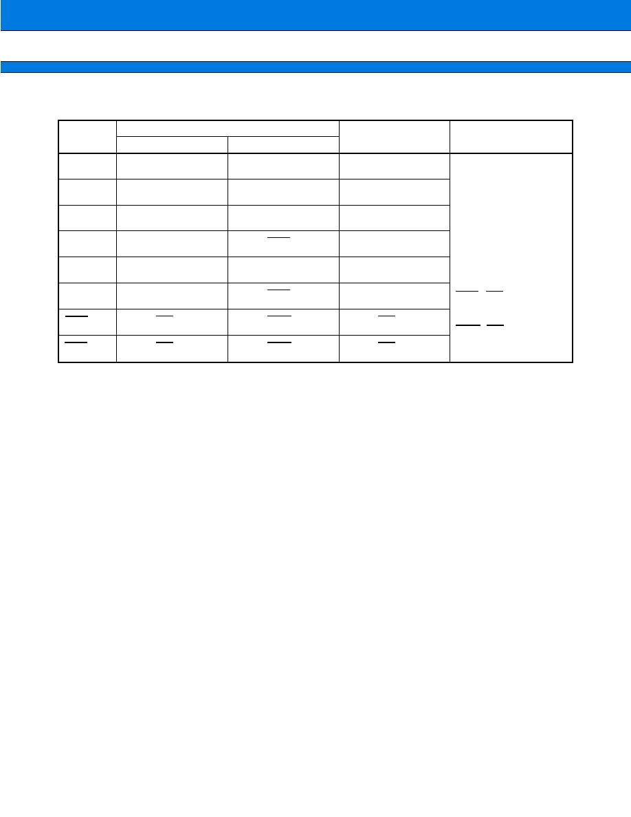
s
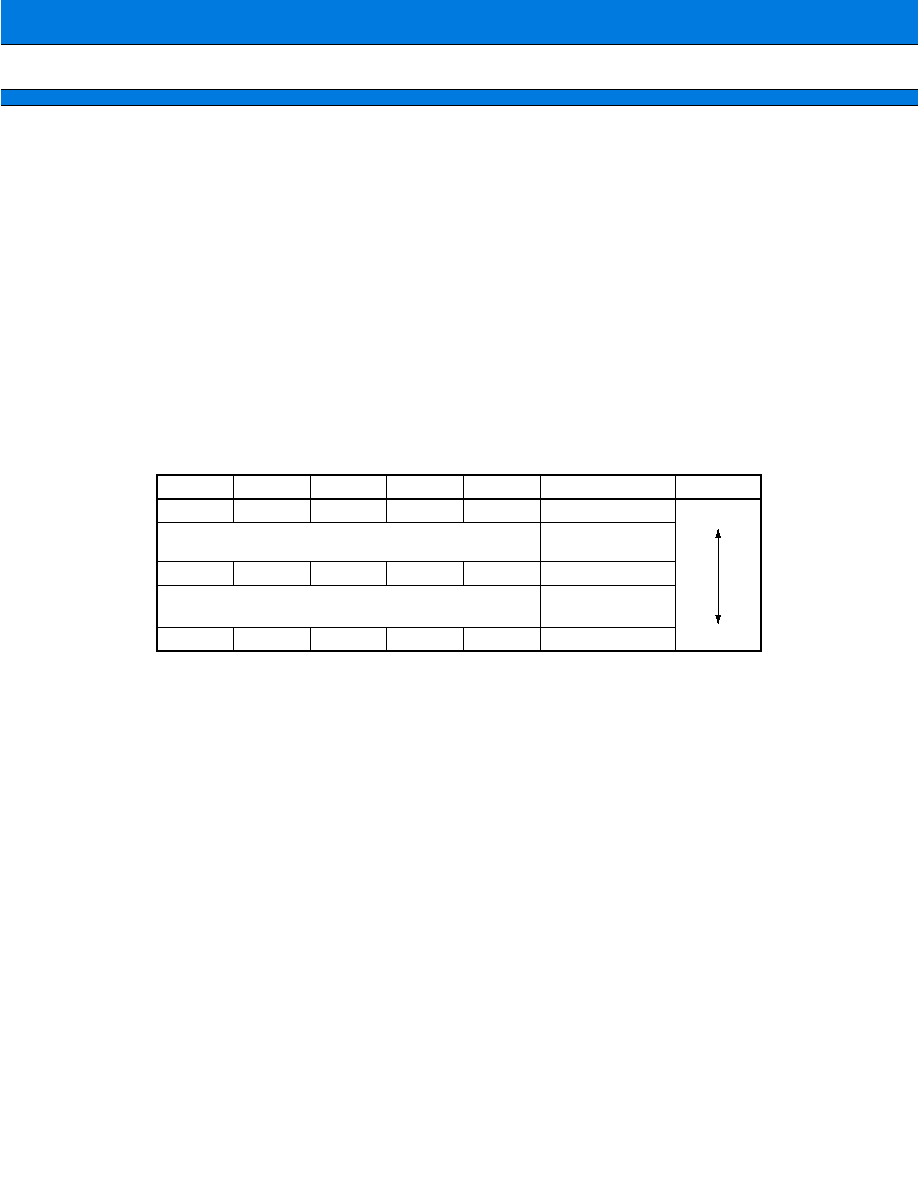
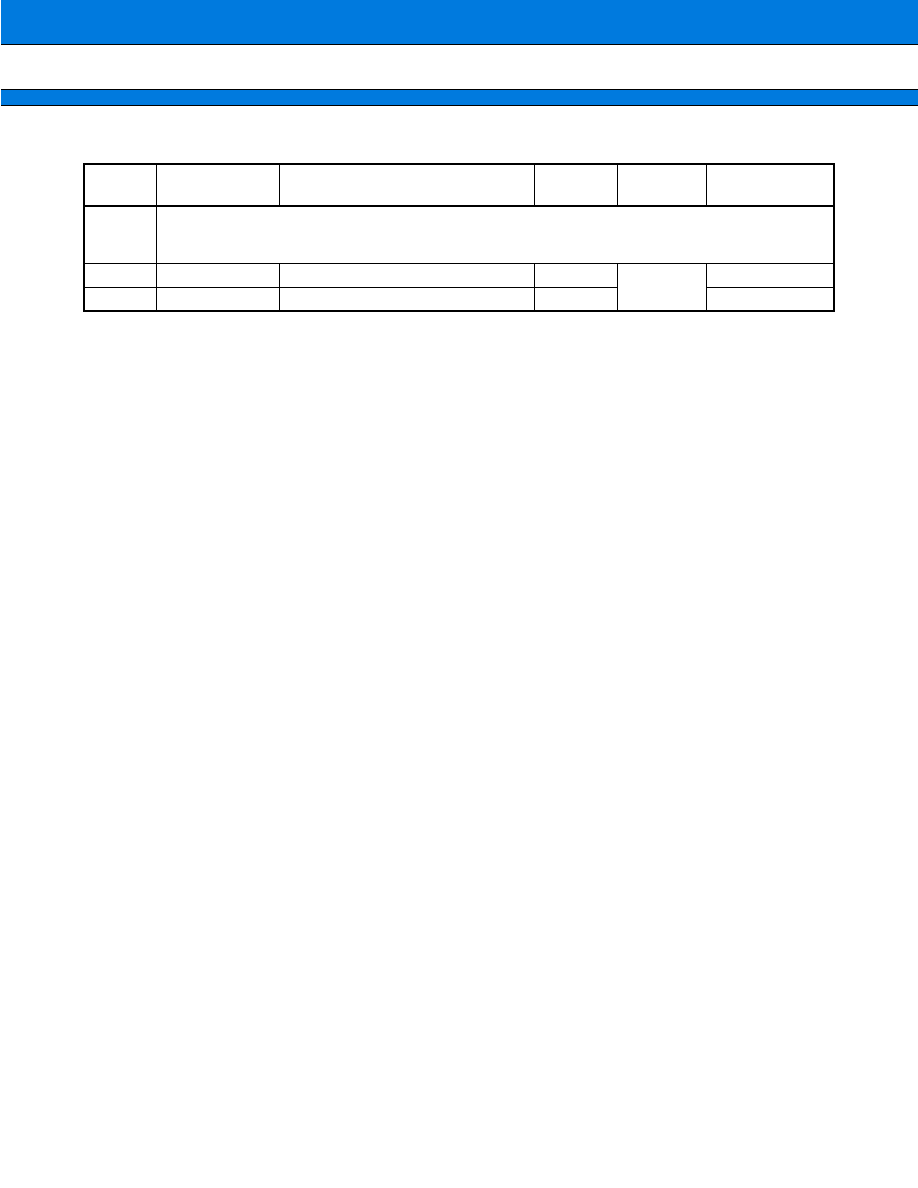
DRAM CONTROL PIN
Pin name
Data bus 16-bit mode
Data bus 8-bit mode
Remarks
2CAS/1WR mode
1CAS/2WR mode
Area 4 RAS
Area 4 RAS
Area 4 RAS
Correspondence of "L"
"H" to lower address 1
bit (A0) in data bus 16-
bit mode
"L": "0"
"H": "1"
CASL: CAS which A0
corresponds to
"0" area
CASH: CAS which A0
corresponds to
"1" area
WEL: WE which A0
corresponds to
"0" area
WEH: WE which A0
corresponds to
"1" area
Area 5 RAS
Area 5 RAS
Area 5 RAS
Area 4 CASL
Area 4 CAS
Area 4 CAS
Area 4 CASH
Area 4 WEL
Area 4 CAS
Area 5 CASL
Area 5 CAS
Area 5 CAS
Area 5 CASH
Area 5 WEL
Area 5 CAS
Area 4 WE
Area 4 WEH
Area 4 WE
DW1
Area 5 WE
Area 5 WEH
Area 5 WE
RAS0
RAS1
CS0L
CS0H
CS1L
CS1H
DW0
MB91106 Series
14
s
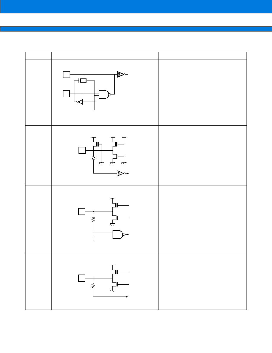
I/O CIRCUIT TYPE
(Continued)
Type
Circuit
Remarks
A
∑ Oscillation feedback resistance 1 M
approx.
With standby control
B
∑ CMOS level hysteresis input
Without standby control
With pull-up resistance
C
∑ CMOS level I/O
With standby control
D
∑ Analog input
Clock input
Standby control signal
X1
X0
V
CC
Digital input
N-channel
type transister
P-channel
type transister
Diffused resistor
V
SS
P-ch
Standby control signal
N-ch
R
P-ch
Digital output
Digital output
Digital input
Digital output
P-ch
Analog input
R
N-ch
Digital output
15
MB91106 Series
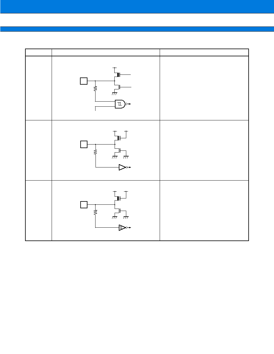
(Continued)
Type
Circuit
Remarks
E
∑ CMOS level output
∑ CMOS level hysteresis input
With standby control
F
∑ CMOS level input
Without standby control
G
∑ CMOS level hysteresis input
Without standby control
Standby control signal
Digital input
Digital output
P-ch
N-ch
R
Digital output
Digital input
R
P-ch
N-ch
Digital input
P-ch
R
Digital input
N-ch
MB91106 Series
16
s
HANDLING DEVICES
1.
Preventing Latchup
In CMOS ICs, applying voltage higher than V
CC
or lower than V
SS
to input/output pin or applying voltage over
rating across V
CC
and V
SS
may cause latchup.
This phenomenon rapidly increases the power supply current, which may result in thermal breakdown of the
device. Make sure to prevent the voltage from exceeding the maximum rating.
Take care that the analog power supply (AV
CC
AVR) and the analog input do not exceed the digital power supply
(V
CC
) when the analog power supply turned on or off.
2.
Treatment of Unused Pins
Unused pins left open may cause malfunctions. Make sure to connect them to pull-up or pull-down resistors.
3.
External Reset Input
It takes at least 5 machine cycle to input "L" level to the RST pin and to ensure inner reset operation properly.
4.
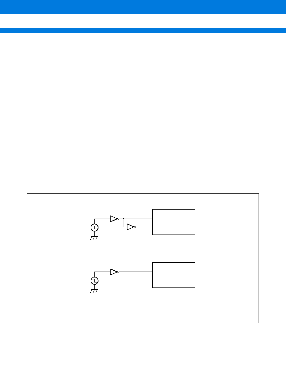
Remarks for External Clock Operation
When external clock is selected, supply it to X0 pin generally, and simultaneously the opposite phase clock to
X0 must be supplied to X1 pin. However, in this case the stop mode must not be used (because X1 pin stops
at "H" output in stop mode).
And can be used to supply only to X0 pin with 5 V power supply at 12.5 MHz and less than.
∑ Using an external clock
Using an external clock (normal)
Note: Can not be used stop mode (oscillation stop mode).
Using an external clock (can be used at 12.5 MHz and less than.)
(5 V power supply only)
MB91106
MB91106
X0
X1
Open
X1
X0

17
MB91106 Series
5.
Power Supply Pins
When there are several V
CC
and V
SS
pins, each of them is equipotentially connected to its counterpart inside
of the device, minimizing the risk of malfunctions such as latch up. To further reduce the risk of malfunctions,
to prevent EMI radiation, to prevent strobe signal malfunction resulting from creeping-up of ground level and
to observe the total output current standard, connect all V
CC
and V
SS
pins to the power supply or GND.
It is preferred to connect V
CC
and V
SS
of MB91106 to power supply with minimal impedance possible.
It is also recommended to connect a ceramic capacitor as a bypass capacitor of about 0.1
µ
F between V
CC
and V
SS
at a position as close as possible to MB91106.
6.
Crystal Oscillator Circuit
Noises around X0 and X1 pins may cause malfunctions of MB91106. In designing the PC board, layout X0,
X1 and crystal oscillator (or ceramic oscillator) and bypass capacitor for grounding as close as possible.
It is strongly recommended to design PC board so that X1 and X0 pins are surrounded by grounding area for
stable operation.
7.
Turning-on Sequence of A/D Converter Power Supply and Analog Input
Make sure to turn on the digital power supply (V
CC
) before turning on the A/D converter (AV
CC
, AVRH) and
applying voltage to analog input (AN0 to AN3).
Make sure to turn off digital power supply after power supply to A/D converters and analog inputs have been
switched off. (There are no such limitations in turning on power supplies. Analog and digital power supplies
may be turned on simultaneously.) Make sure that AVRH never exceeds AV
CC
when turning on/off power
supplies.
8.
Treatment of N.C. Pins
Make sure to leave N.C. pins open.
9.
Fluctuation of Power Supply Voltage
Warranty range for normal operation against fluctuation of power supply voltage V
CC
is as given in rating.
However, sudden fluctuation of power supply voltage within the warranty range may cause malfunctions. It is
recommended to make every effort to stabilize the power supply voltage to IC. It is also recommended that by
controlling power supply as a reference of stabilizing, V
CC
ripple fluctuation (P-P value) at the commercial
frequency (50 Hz to 60 Hz) should be less than 10% of the standard V
CC
value and the transient regulation
should be less than 0.1 V/ms at instantaneous deviation like turning off the power supply.
10. Mode Setting Pins (MD0 to MD2)
Connect mode setting pins (MD0 to MD2) directly to V
CC
or V
SS
.
Arrange each mode setting pin and V
CC
or V
SS
patterns on the printed circuit board as close as possible and
make the impedance between them minimal to prevent mistaken entrance to the test mode caused by noises.
11. Turning on the Power Supply
When turning on the power supply, never fail to start from setting the RST pin to "L" level. And after the power
supply voltage goes to V
CC
level, at least after ensuring the time for 5 machine cycle, then set to "H" level.

MB91106 Series
18
12. Pin Condition at Turning on the Power Supply
The pin condition at turning on the power supply is unstable. The circuit starts being initialized after turning on
the power supply and then starting oscillation and then the operation of the internal regulator becomes stable.
So it takes about 42 ms for the pin to be initialized from the oscillation starting at the source oscillation 12.5
MHz. Take care that the pin condition may be output condition at initial unstable condition.
13. Source Oscillation Input at Turning on the Power Supply
At turning on the power supply, never fail to input the clock before cancellation of the oscillation stabilizing
waiting.
14. Initialization
Some internal resistors initialized only via power on reset are embedded in the device. To initialize these
resistors, run power on reset by returning on the power supply or to set RST pin to "H" level.
19
MB91106 Series
s
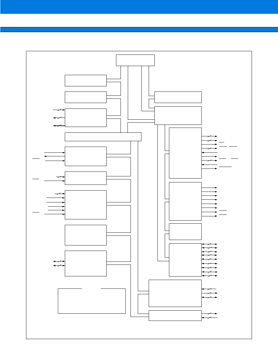
BLOCK DIAGRAM
8
8
8
8
8
6
7
8
Note: Pins are display for functions (Actually some pins are multiplexer).
When using REALOS, time control should be done by using external interrupt or inner timer.
FR CPU
RAM (2 Kbytes)
Bit search module
DMA controller (DMAC)
(8 ch.)
Bus converter (32 bits
16bits)
Clock control unit
(Watchdog timer)
Interrupt control unit
10-bit A/D converter
(4 ch.)
16-bit reload timer (3 ch.)
Port E,
Port F
D-b
u
s (32 bits)
I-b
u
s (16 bits)
Instruction ROM
63 Kbytes, 32bits
Bus converter
(Harvard
Princeton)
Bus controller
DRAM interface
Instruction ROM
and
data ROM
64 Kbytes
Port 2 to port B
UART (3 ch.)
(Baud rate timer)
PWM timer (4 ch.)
Other pins
MD0 to MD2, V
CC
, V
SS
DREQ0 to
DREQ2
DACK0 to
DACK2
EOP0 to
EOP2
X0
X1
RST
INT0 to INT3
NMI
AN0 to AN3
AV
CC
AV
SS
AVRH
AVRL
ATG
PE0 to PE7
PF0 to PF7
3
3
3
4
4
8
8
R-b
u
s (16 bits)
C-b
u
s (32 bits)
D16 to D31
A00 to A24
RD
WR0, WR1
RDY
CLK
CS0 to CS5
BRQ
BGRNT
RAS0
RAS1
CS0L
CS0H
CS1L
CS1H
DW0
DW1
P20 to P27
P30 to P37
P40 to P47
P50 to P57
P60 to P67
P70
PA80 to P85
PA0 to PA6
PB0 to PB7
SI0 to SI2
SO0 to SO2
SC0 to SC2
OCPA0 to OCPA3
TRG0 to TRG3
16
2
25
6
3
3
3
4
4
MB91106 Series
20
s
CPU CORE
1.
Memory Space
The FR family has a logical address space of 4 Gbytes (2
32
bytes) and the CPU linearly accesses the memory
space.
∑ Memory space
* : Direct addressing area
The following areas on the memory space are assigned to direct addressing area for I/O. In these areas, an
address can be specified in a direct operand of a code.
Direct areas consists of the following areas dependent on accessible data sizes.
Byte data access: 000
H
to 0FF
H
Half word data access: 000
H
to 1FF
H
Word data access: 000
H
to 3FF
H
Notes:
∑
Access to the external area can be execute in the single chip mode.
To access to the external area, select internal ROM external bus mode via mode resistor.
Never execute data access to the instruction ROM area.
∑
In the instruction/data ROM, images in block of 64 Kbytes can be seen.
Make an instruction/data in the area 000F0000
H
to 000FFFFF
H
.
See "
s
I/O MAP"
Direct
addressing
area*
Single chip mode
∑
Memory Space
Internal ROM/
external bus mode
External ROM/
external bus mode
Address
0000 0000
H
0000 0400
H
0000 0800
H
0000 1000
H
0000 1800
H
0001 0000
H
0008 0000
H
0008 FC00
H
000F 0000
H
0010 0000
H
FFFF FFFF
H
I/0 Area
I/0 Area
Access inhibited
Embedded RAM
(2 Kbytes)
Access inhibited
Access inhibited
Instruction ROM
(63 Kbytes)
Access inhibited
Instruction ROM/data ROM
(64 Kbytes)
Access inhibited
I/0 Area
I/0 Area
Access inhibited
Embedded RAM
(2 Kbytes)
Access inhibited
External area
Instruction ROM
(63 Kbytes)
Access inhibited
Instruction ROM/data ROM
(64 Kbytes)
External area
I/0 Area
I/0 Area
Access inhibited
Embedded RAM
(2 Kbytes)
Access inhibited
External area
21
MB91106 Series
2.
Registers
The FR family has two types of registers; dedicated registers embedded on the CPU and general-purpose
registers on memory.
∑ Dedicated registers
Program counter (PC):
32-bit length, indicates the location of the instruction to be executed.
Program status (PS):
32-bit length, register for storing register pointer or condition codes
Table base register (TBR):
Holds top address of vector table used in EIT (Exceptional/Interrupt/Trap)
processing.
Return pointer (RP):
Holds address to resume operation after returning from a subroutine.
System stack pointer (SSP): Indicates system stack space.
User's stack pointer (USP): Indicates user's stack space.
Multiplication/division result register (MDH/MDL): 32-bit length, register for multiplication/division
∑ Program status (PS)
The PS register is for holding program status and consists of a condition code register (CCR), a system condition
code register (SCR) and a interrupt level mask register (ILM).
PC
PS
TBR
RP
SSP
USP
MDH
MDL
Initial value
Program counter
Program status
Table base register
Return pointer
System stack pointer
User's stack pointer
Multiplication/division result register
XXXX XXXX
H
Indeterminate
000F
FC00
H
XXXX XXXX
H
Indeterminate
0000
0000
H
XXXX XXXX
H
Indeterminate
XXXX XXXX
H
Indeterminate
XXXX XXXX
H
Indeterminate
32 bits
--
ILM4 ILM3 ILM2 ILM1
--
ILM0
D1
D0
T
--
S
--
Z
C
V
N
I
31
20
19
18
17
16
10
9
8
7
5
6
2
0
1
3
4
ILM
SCR
CCR
PS
MB91106 Series
22
∑ Condition code register (CCR)
S-flag:
Specifies a stack pointer used as R15.
I-flag:
Controls user interrupt request enable/disable.
N-flag:
Indicates sign bit when division result is assumed to be in the 2's complement format.
Z-flag:
Indicates whether or not the result of division was "0".
V-flag:
Assumes the operand used in calculation in the 2's complement format and indicates whether
or not overflow has occurred.
C-flag:
Indicates if a carry or borrow from the MSB has occurred.
∑ System condition code register (SCR)
T-flag:
Specifies whether or not to enable step trace trap.
∑ Interrupt level mask register (ILM)
ILM4 to ILM0: Register for holding interrupt level mask value. The value held by this register is used as a
level mask. When an interrupt request issued to the CPU is higher than the level held by ILM,
the interrupt request is accepted.
ILM4
ILM3
ILM2
ILM1
ILM0
Interrupt level
High-low
0
0
0
0
0
0
High
:
:
:
:
0
1
0
0
0
15
:
:
:
:
1
1
1
1
1
31
Low
23
MB91106 Series
s
GENERAL-PURPOSE REGISTERS
R0 to R15 are general-purpose registers embedded on the CPU. These registers functions as an accumulator
and a memory access pointer (field for indicating address).
Of the above 16 registers, following registers have special functions. To support the special functions, part of
the instruction set has been sophisticated to have enhanced functions.
R13: Virtual accumulator (AC)
R14: Frame pointer (FP)
R15: Stack pointer (SP)
Upon reset, values in R0 to R14 are not fixed. Value in R15 is initialized to be 0000 0000
H
(SSP value).
∑ Register bank structure
R0
R1
R12
R13
R14
R15
AC (accumulator)
FP (frame pointer)
SP (stack pointer)
32 bits
:
:
Initial value
XXXX XXXX
H
:
:
:
:
:
:
:
:
:
:
:
XXXX XXXX
H
0 0 0 0 0 0 0 0
H
MB91106 Series
24
s
SETTING MODE
1.
Pin
∑ Mode setting pins and modes
* : MB91106 support single-chip mode.
2.
Registers
∑ Mode setting registers (MODR) and modes
∑ Bus mode setting bits and functions
Mode setting
pins
Mode name
Reset vector
access area
External data
bus width
Bus mode
MD2 MD1 MD0
0
0
0
External vector mode 0
External
8 bits
External ROM/external bus
mode
0
0
1
External vector mode 1
External
16 bits
0
1
0
--
--
--
Inhibited
0
1
1
Internal vector mode
Internal
(Mode register)
Single-chip mode*
1
--
--
--
--
--
Not use
M1
M0
Functions
Note
0
0
Single-chip mode
0
1
Internal ROM/external bus mode
1
0
External ROM/external bus mode
1
1
--
Inhibited
M1
M0
*
*
*
*
*
*
Address
0000 07FF
H
Bus mode setting bit
W : Write only
X : Indeterminate
* : Always write "0" except for M1 and M0.
Initial value
XXXX XXXX
B
Access
W
25
MB91106 Series
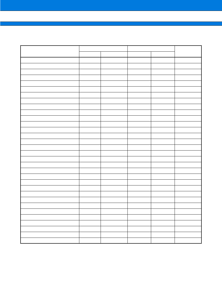
s
I/O MAP
(Continued)
Address
Register name
(abbreviated)
Register name
Read/write
Resources
name
Initial value
000000
H
PDR3
Port 3 data register
R/W
Port 3
X X X X X X X X
B
000001
H
PDR2
Port 2 data register
R/W
Port 2
X X X X X X X X
B
000002
H
(Vacancy)
000003
H
000004
H
PDR7
Port 7 data register
R/W
Port 7
≠ ≠ ≠ ≠ ≠ ≠ ≠ X
B
000005
H
PDR6
Port 6 data register
R/W
Port 6
X X X X X X X X
B
000006
H
PDR5
Port 5 data register
R/W
Port 5
X X X X X X X X
B
000007
H
PDR4
Port 4 data register
R/W
Port 4
X X X X X X X X
B
000008
H
PDRB
Port B data register
R/W
Port B
X X X X X X X X
B
000009
H
PDRA
Port A data register
R/W
Port A
≠ X X X X X X X
B
00000A
H
(Vacancy)
00000B
H
PDR8
Port 8 data register
R/W
Port 8
≠ ≠ X X X X X X
B
00000C
H
to
000011
H
(Vacancy)
000012
H
PDRE
Port E data register
R/W
Port E
X X X X X X X X
B
000013
H
PDRF
Port F data register
R/W
Port F
X X X X X X X X
B
000014
H
to
00001B
H
(Vacancy)
00001C
H
SSR0
Serial status register 0
R/W
UART0
0 0 0 0 1 ≠ 0 0
B
00001D
H
SIDR0/SODR0
Serial input data register 0/serial
output data register 0
R/W
X X X X X X X X
B
00001E
H
SCR0
Serial control register 0
R/W
0 0 0 0 0 1 0 0
B
00001F
H
SMR0
Serial mode register 0
R/W
0 0 ≠ ≠ 0 ≠ 0 0
B
000020
H
SSR1
Serial status register 1
R/W
UART1
0 0 0 0 1 ≠ 0 0
B
000021
H
SIDR1/SODR1
Serial input data register 1/serial
output data register 1
R/W
X X X X X X X X
B
000022
H
SCR1
Serial control register 1
R/W
0 0 0 0 0 1 0 0
B
000023
H
SMR1
Serial mode register 1
R/W
0 0 ≠ ≠ 0 ≠ 0 0
B
000024
H
SSR2
Serial status register 2
R/W
UART2
0 0 0 0 1 ≠ 0 0
B
000025
H
SIDR2/SODR2
Serial input data register 2/serial
output data register 2
R/W
X X X X X X X X
B
000026
H
SCR2
Serial control register 2
R/W
0 0 0 0 0 1 0 0
B
000027
H
SMR2
Serial mode register 2
R/W
0 0 ≠ ≠ 0 ≠ 0 0
B
MB91106 Series
26
(Continued)
Address
Register name
(abbreviated)
Register name
Read/write
Resources
name
Initial value
000028
H
TMRLR0
16-bit reload register 0
W
16-bit reload
timer 0
X X X X X X X X
B
000029
H
X X X X X X X X
B
00002A
H
TMR0
16-bit timer register 0
R
X X X X X X X X
B
00002B
H
X X X X X X X X
B
00002C
H
(Vacancy)
00002D
H
00002E
H
TMCSR0
16-bit reload timer control status
register 0
R/W
16-bit reload
timer 0
≠ ≠ ≠ ≠ 0 0 0 0
B
00002F
H
0 0 0 0 0 0 0 0
B
000030
H
TMRLR1
16-bit reload register 1
W
16-bit reload
timer 1
X X X X X X X X
B
000031
H
X X X X X X X X
B
000032
H
TMR1
16-bit timer register 1
R
X X X X X X X X
B
000033
H
X X X X X X X X
B
000034
H
(Vacancy)
000035
H
000036
H
TMCSR1
16-bit reload timer control status
register 1
R/W
16-bit reload
timer 1
≠ ≠ ≠ ≠ 0 0 0 0
B
000037
H
0 0 0 0 0 0 0 0
B
000038
H
ADCR
A/D converter data register
R
10-bit A/D
converter
0 0 0 0 0 0 X X
B
000039
H
X X X X X X X X
B
00003A
H
ADCS
A/D converter control status register
R/W
0 0 0 0 0 0 0 0
B
00003B
H
0 0 0 0 0 0 0 0
B
00003C
H
TMRLR2
16-bit reload register 2
W
16-bit reload
timer 2
X X X X X X X X
B
00003D
H
X X X X X X X X
B
00003E
H
TMR2
16-bit timer register 2
R
X X X X X X X X
B
00003F
H
X X X X X X X X
B
000040
H
(Vacancy)
000041
H
000042
H
TMCSR2
16-bit reload timer control status
register 2
R/W
16-bit reload
timer 2
≠ ≠ ≠ ≠ 0 0 0 0
B
000043
H
0 0 0 0 0 0 0 0
B
000044
H
to
000077
H
(Vacancy)
27
MB91106 Series
(Continued)
Address
Register name
(abbreviated)
Register name
Read/write
Resources
name
Initial value
000078
H
UTIM0/UTIMR0
U-TIMER register ch. 0 /U-TIMER
reload register ch. 0
R/W
U-TIMER 0
0 0 0 0 0 0 0 0
B
000079
H
0 0 0 0 0 0 0 0
B
00007A
H
(Vacancy)
00007B
H
UTIMC0
U-TIMER control register ch. 0
R/W
U-TIMER 0
0 ≠ ≠ 0 0 0 0 1
B
00007C
H
UTIM1/UTIMR1
U-TIMER register ch. 1/reload
register ch. 1
R/W
U-TIMER 1
0 0 0 0 0 0 0 0
B
00007D
H
0 0 0 0 0 0 0 0
B
00007E
H
(Vacancy)
00007F
H
UTIMC1
U-TIMER control register ch. 1
R/W
U-TIMER 1
0 ≠ ≠ 0 0 0 0 1
B
000080
H
UTIM2/UTIMR2
U-TIMER register ch. 2/U-TIMER
reload register ch. 2
R/W
U-TIMER 2
0 0 0 0 0 0 0 0
B
000081
H
0 0 0 0 0 0 0 0
B
000082
H
(Vacancy)
000083
H
UTIMC2
U-TIMER control register ch. 2
R/W
U-TIMER 2
0 ≠ ≠ 0 0 0 0 1
B
000084
H
to
000093
H
(Vacancy)
000094
H
EIRR
External interrupt cause register
R/W
External
interrupt/
NMI
0 0 0 0 0 0 0 0
B
000095
H
ENIR
Interrupt enable register
R/W
0 0 0 0 0 0 0 0
B
000096
H
to
000098
H
(Vacancy)
000099
H
ELVR
External interrupt request level
setting register
R/W
External
interrupt/
NMI
0 0 0 0 0 0 0 0
B
00009A
H
to
0000D1
H
(Vacancy)
0000D2
H
DDRE
Port E data direction register
W
Port E
0 0 0 0 0 0 0 0
B
0000D3
H
DDRF
Port F data direction register
W
Port F
0 0 0 0 0 0 0 0
B
0000D4
H
to
0000DB
H
(Vacancy)
0000DC
H
GCN1
General control register 1
R/W
PWM
timer 1
0 0 1 1 0 0 1 0
B
0000DD
H
0 0 0 1 0 0 0 0
B
0000DE
H
(Vacancy)
0000DF
H
GCN2
General control register 2
R/W
PWM
timer 2
0 0 0 0 0 0 0 0
B
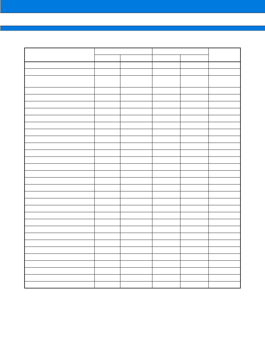
MB91106 Series
28
(Continued)
Address
Register name
(abbreviated)
Register name
Read/write
Resources
name
Initial value
0000E0
H
PTMR0
PWM timer register 0
R
PWM
timer 0
1 1 1 1 1 1 1 1
B
0000E1
H
1 1 1 1 1 1 1 1
B
0000E2
H
PCSR0
PWM cycle setting register 0
W
X X X X X X X X
B
0000E3
H
X X X X X X X X
B
0000E4
H
PDUT0
PWM duty setting register 0
W
X X X X X X X X
B
0000E5
H
X X X X X X X X
B
0000E6
H
PCNH0
Control status register H 0
R/W
0 0 0 0 0 0 0 ≠
B
0000E7
H
PCNL0
Control status register L 0
R/W
0 0 0 0 0 0 0 0
B
0000E8
H
PTMR1
PWM timer register 1
R
PWM
timer 1
1 1 1 1 1 1 1 1
B
0000E9
H
1 1 1 1 1 1 1 1
B
0000EA
H
PCSR1
PWM cycle setting register 1
W
X X X X X X X X
B
0000EB
H
X X X X X X X X
B
0000EC
H
PDUT1
PWM duty setting register 1
W
X X X X X X X X
B
0000ED
H
X X X X X X X X
B
0000EE
H
PCNH1
Control status register H 1
R/W
0 0 0 0 0 0 0 ≠
B
0000EF
H
PCNL1
Control status register L 1
R/W
0 0 0 0 0 0 0 0
B
0000F0
H
PTMR2
PWM timer register 2
R
PWM
timer 2
1 1 1 1 1 1 1 1
B
0000F1
H
1 1 1 1 1 1 1 1
B
0000F2
H
PCSR2
PWM cycle setting register 2
W
X X X X X X X X
B
0000F3
H
X X X X X X X X
B
0000F4
H
PDUT2
PWM duty setting register 2
W
X X X X X X X X
B
0000F5
H
X X X X X X X X
B
0000F6
H
PCNH2
Control status register H 2
R/W
0 0 0 0 0 0 0 ≠
B
0000F7
H
PCNL2
Control status register L 2
R/W
0 0 0 0 0 0 0 0
B
0000F8
H
PTMR3
PWM timer register 3
R
PWM
timer 3
1 1 1 1 1 1 1 1
B
0000F9
H
1 1 1 1 1 1 1 1
B
0000FA
H
PCSR3
PWM cycle setting register 3
W
X X X X X X X X
B
0000FB
H
X X X X X X X X
B
0000FC
H
PDUT3
PWM duty setting register 3
W
X X X X X X X X
B
0000FD
H
X X X X X X X X
B
0000FE
H
PCNH3
Control status register H 3
R/W
0 0 0 0 0 0 0 ≠
B
0000FF
H
PCNL3
Control status register L 3
R/W
0 0 0 0 0 0 0 0
B
29
MB91106 Series
(Continued)
Address
Register name
(abbreviated)
Register name
Read/write
Resources
name
Initial value
000100
H
to
0001FF
H
(Vacancy)
000200
H
DPDP
DMAC parameter descriptor pointer
R/W
DMA
controller
(DMAC)
X X X X X X X X
B
000201
H
X X X X X X X X
B
000202
H
X X X X X X X X
B
000203
H
X 0 0 0 0 0 0 0
B
000204
H
DACSR
DMAC control status register
R/W
0 0 0 0 0 0 0 0
B
000205
H
0 0 0 0 0 0 0 0
B
000206
H
0 0 0 0 0 0 0 0
B
000207
H
0 0 0 0 0 0 0 0
B
000208
H
DATCR
DMAC pin control register
R/W
X X X X X X X X
B
000209
H
X X 0 0 0 0 0 0
B
00020A
H
X X 0 0 0 0 0 0
B
00020B
H
X X 0 0 0 0 0 0
B
00020C
H
to
0003EF
H
(Vacancy)
0003F0
H
BSD0
Bit search module 0-detection data
register
W
Bit search
module
X X X X X X X X
B
0003F1
H
X X X X X X X X
B
0003F2
H
X X X X X X X X
B
0003F3
H
X X X X X X X X
B
0003F4
H
BSD1
Bit search module 1-detection data
register
R/W
X X X X X X X X
B
0003F5
H
X X X X X X X X
B
0003F6
H
X X X X X X X X
B
0003F7
H
X X X X X X X X
B
0003F8
H
BSDC
Bit search module transition-
detection data register
W
X X X X X X X X
B
0003F9
H
X X X X X X X X
B
0003FA
H
X X X X X X X X
B
0003FB
H
X X X X X X X X
B
0003FC
H
BSRR
Bit search module detection result
register
R
X X X X X X X X
B
0003FD
H
X X X X X X X X
B
0003FE
H
X X X X X X X X
B
0003FF
H
X X X X X X X X
B
MB91106 Series
30
(Continued)
Address
Register name
(abbreviated)
Register name
Read/write
Resources
name
Initial value
000400
H
ICR00
Interrupt control register 0
R/W
Interrupt
controller
≠ ≠ ≠ 1 1 1 1 1
B
000401
H
ICR01
Interrupt control register 1
R/W
≠ ≠ ≠ 1 1 1 1 1
B
000402
H
ICR02
Interrupt control register 2
R/W
≠ ≠ ≠ 1 1 1 1 1
B
000403
H
ICR03
Interrupt control register 3
R/W
≠ ≠ ≠ 1 1 1 1 1
B
000404
H
ICR04
Interrupt control register 4
R/W
≠ ≠ ≠ 1 1 1 1 1
B
000405
H
ICR05
Interrupt control register 5
R/W
≠ ≠ ≠ 1 1 1 1 1
B
000406
H
ICR06
Interrupt control register 6
R/W
≠ ≠ ≠ 1 1 1 1 1
B
000407
H
ICR07
Interrupt control register 7
R/W
≠ ≠ ≠ 1 1 1 1 1
B
000408
H
ICR08
Interrupt control register 8
R/W
≠ ≠ ≠ 1 1 1 1 1
B
000409
H
ICR09
Interrupt control register 9
R/W
≠ ≠ ≠ 1 1 1 1 1
B
00040A
H
ICR10
Interrupt control register 10
R/W
≠ ≠ ≠ 1 1 1 1 1
B
00040B
H
ICR11
Interrupt control register 11
R/W
≠ ≠ ≠ 1 1 1 1 1
B
00040C
H
ICR12
Interrupt control register 12
R/W
≠ ≠ ≠ 1 1 1 1 1
B
00040D
H
ICR13
Interrupt control register 13
R/W
≠ ≠ ≠ 1 1 1 1 1
B
00040E
H
ICR14
Interrupt control register 14
R/W
≠ ≠ ≠ 1 1 1 1 1
B
00040F
H
ICR15
Interrupt control register 15
R/W
≠ ≠ ≠ 1 1 1 1 1
B
000410
H
ICR16
Interrupt control register 16
R/W
≠ ≠ ≠ 1 1 1 1 1
B
000411
H
ICR17
Interrupt control register 17
R/W
≠ ≠ ≠ 1 1 1 1 1
B
000412
H
ICR18
Interrupt control register 18
R/W
≠ ≠ ≠ 1 1 1 1 1
B
000413
H
ICR19
Interrupt control register 19
R/W
≠ ≠ ≠ 1 1 1 1 1
B
000414
H
ICR20
Interrupt control register 20
R/W
≠ ≠ ≠ 1 1 1 1 1
B
000415
H
ICR21
Interrupt control register 21
R/W
≠ ≠ ≠ 1 1 1 1 1
B
000416
H
ICR22
Interrupt control register 22
R/W
≠ ≠ ≠ 1 1 1 1 1
B
000417
H
ICR23
Interrupt control register 23
R/W
≠ ≠ ≠ 1 1 1 1 1
B
000418
H
ICR24
Interrupt control register 24
R/W
≠ ≠ ≠ 1 1 1 1 1
B
000419
H
ICR25
Interrupt control register 25
R/W
≠ ≠ ≠ 1 1 1 1 1
B
00041A
H
ICR26
Interrupt control register 26
R/W
≠ ≠ ≠ 1 1 1 1 1
B
00041B
H
ICR27
Interrupt control register 27
R/W
≠ ≠ ≠ 1 1 1 1 1
B
00041C
H
ICR28
Interrupt control register 28
R/W
≠ ≠ ≠ 1 1 1 1 1
B
00041D
H
ICR29
Interrupt control register 29
R/W
≠ ≠ ≠ 1 1 1 1 1
B
00041E
H
ICR30
Interrupt control register 30
R/W
≠ ≠ ≠ 1 1 1 1 1
B
00041F
H
ICR31
Interrupt control register 31
R/W
≠ ≠ ≠ 1 1 1 1 1
B
31
MB91106 Series
(Continued)
Address
Register name
(abbreviated)
Register name
Read/write
Resources
name
Initial value
000420
H
to
00042E
H
(Vacancy)
00042F
H
ICR47
Interrupt control register 47
R/W
Interrupt
controller
≠ ≠ ≠ 1 1 1 1 1
B
000430
H
DICR
Delayed interrupt control register
R/W
≠ ≠ ≠ ≠ ≠ ≠ ≠ 0
B
000431
H
HRCL
Hold request cancel request level
setting register
R/W
≠ ≠ ≠ 1 1 1 1 1
B
000432
H
to
00047F
H
(Vacancy)
000480
H
RSRR/WTCR
Reset cause register/
watchdog cycle control register
R/W
Clock
control
1X X X X ≠ 0 0
B
000481
H
STCR
Standby control register
R/W
0 0 0 1 1 1 ≠ ≠
B
000482
H
PDRR
DMA controller request squelch
register
R/W
≠ ≠ ≠ ≠ 0 0 0 0
B
000483
H
CTBR
Timebase timer clear register
W
X X X X X X X X
B
000484
H
GCR
Gear control register
R/W
1 1 0 0 1 1 ≠ 1
B
000485
H
WPR
Watchdog reset occurrence postpone
register
W
X X X X X X X X
B
000486
H
(Vacancy)
000487
H
000488
H
PCTR
PLL control register
R/W
PLL control
0 0 ≠ ≠ 0 ≠ ≠ ≠
B
000489
H
to
0005FF
H
(Vacancy)
000600
H
DDR3
Port 3 data direction register
W
Port 3
0 0 0 0 0 0 0 0
B
000601
H
DDR2
Port 2 data direction register
W
Port 2
0 0 0 0 0 0 0 0
B
000602
H
to
000603
H
(Vacancy)
000604
H
DDR7
Port 7 data direction register
W
Port 7
≠ ≠ ≠ ≠ ≠ ≠ ≠ 0
B
000605
H
DDR6
Port 6 data direction register
W
Port 6
0 0 0 0 0 0 0 0
B
000606
H
DDR5
Port 5 data direction register
W
Port 5
0 0 0 0 0 0 0 0
B
000607
H
DDR4
Port 4 data direction register
W
Port 4
0 0 0 0 0 0 0 0
B
000608
H
DDRB
Port B data direction register
W
Port B
0 0 0 0 0 0 0 0
B
000609
H
DDRA
Port A data direction register
W
Port A
≠ 0 0 0 0 0 0 0
B
00060A
H
(Vacancy)
00060B
H
DDR8
Port 8 data direction register
W
Port 8
≠ ≠ 0 0 0 0 0 0
B
MB91106 Series
32
(Continued)
Address
Register name
(abbreviated)
Register name
Read/write
Resources
name
Initial value
00060C
H
ASR1
Area select register 1
W
External bus
interface
0 0 0 0 0 0 0 0
B
00060D
H
0 0 0 0 0 0 0 1
B
00060E
H
AMR1
Area mask register 1
W
0 0 0 0 0 0 0 0
B
00060F
H
0 0 0 0 0 0 0 0
B
000610
H
ASR2
Area select register 2
W
0 0 0 0 0 0 0 0
B
000611
H
0 0 0 0 0 0 1 0
B
000612
H
AMR2
Area mask register 2
W
0 0 0 0 0 0 0 0
B
000613
H
0 0 0 0 0 0 0 0
B
000614
H
ASR3
Area select register 3
W
0 0 0 0 0 0 0 0
B
000615
H
0 0 0 0 0 0 1 1
B
000616
H
AMR3
Area mask register 3
W
0 0 0 0 0 0 0 0
B
000617
H
0 0 0 0 0 0 0 0
B
000618
H
ASR4
Area select register 4
W
0 0 0 0 0 0 0 0
B
000619
H
0 0 0 0 0 1 0 0
B
00061A
H
AMR4
Area mask register 4
W
0 0 0 0 0 0 0 0
B
00061B
H
0 0 0 0 0 0 0 0
B
00061C
H
ASR5
Area select register 5
W
0 0 0 0 0 0 0 0
B
00061D
H
0 0 0 0 0 1 0 1
B
00061E
H
AMR5
Area mask register 5
W
0 0 0 0 0 0 0 0
B
00061F
H
0 0 0 0 0 0 0 0
B
000620
H
AMD0
Area mode register 0
R/W
≠ ≠ ≠ 0 0 1 1 1
B
000621
H
AMD1
Area mode register 1
R/W
0 ≠ ≠ 0 0 0 0 0
B
000622
H
AMD32
Area mode register 32
R/W
0 0 0 0 0 0 0 0
B
000623
H
AMD4
Area mode register 4
R/W
0 ≠ ≠ 0 0 0 0 0
B
000624
H
AMD5
Area mode register 5
R/W
0 ≠ ≠ 0 0 0 0 0
B
000625
H
DSCR
DRAM signal control register
W
0 0 0 0 0 0 0 0
B
000626
H
RFCR
Refresh control register
R/W
≠ ≠ X X X X X X
B
000627
H
0 0 ≠ ≠ ≠ 0 0 0
B
000628
H
EPCR0
External pin control register 0
W
≠ ≠ ≠ ≠ 1 1 0 0
B
000629
H
≠ 1 1 1 1 1 1 1
B
00062A
H
EPCR1
External pin control register 1
W
≠ ≠ ≠ ≠ ≠ ≠ ≠ 1
B
00062B
H
1 1 1 1 1 1 1 1
B
00062C
H
DMCR4
DRAM control register 4
R/W
0 0 0 0 0 0 0 0
B
00062D
H
0 0 0 0 0 0 0 ≠
B
00062E
H
DMCR5
DRAM control register 5
R/W
0 0 0 0 0 0 0 0
B
00062F
H
0 0 0 0 0 0 0 ≠
B
33
MB91106 Series
(Continued)
About Programming
R/W: Readable and writable
R: Read only
W: Write only
Explanation of initial values
0: The initial value of this bit is "0".
1: The initial value of this bit is "1".
X: The initial value of this bit is undefined.
≠: This bit is not used. The initial value of this bit is undefined.
RMW system instructions (RMW: Read Modify Write)
Notes:
∑
Never execute a RMW system instruction to the resistor has a write only bit.
∑
The area "vacancy" on the I/O map is reserved area. Access to this area are deal with to an internal area.
No access signals to the external area would be generated.
Address
Register name
(abbreviated)
Register name
Read/write
Resources
name
Initial value
000630
H
to
0007FD
H
(Vacancy)
0007FE
H
LER
Little endian register
W
External bus
interface
≠ ≠ ≠ ≠ ≠ 0 0 0
B
0007FF
H
MODR
Mode register
W
X X X X X X X X
B
AND
ANDH
ANDB
BANDL
BANDH
Rj, @ Ri
Rj, @ Ri
Rj, @ Ri
#
µ
4, @ Ri
#
µ
4, @ Ri
OR
ORH
ORB
BORL
BORH
Rj, @ Ri
Rj, @ Ri
Rj, @ Ri
#
µ
4, @ Ri
#
µ
4, @ Ri
EOR
EORH
EORB
BEORL
BEORH
Rj, @ Ri
Rj, @ Ri
Rj, @ Ri
#
µ
4, @ Ri
#
µ
4, @ Ri
MB91106 Series
34
s
INTERRUPT CAUSES, INTERRUPT VECTORS
AND INTERRUPT CONTROL REGISTER ALLOCATIONS
(Continued)
Interrupt causes
Interrupt number
Interrupt level
TBR default
address
Decimal
Hexadecimal
Register
Offset
Reset
0
00
--
3FC
H
000FFFFC
H
Reserved for system
1
01
--
3F8
H
000FFFF8
H
Reserved for system
2
02
--
3F4
H
000FFFF4
H
Reserved for system
3
03
--
3F0
H
000FFFF0
H
Reserved for system
4
04
--
3EC
H
000FFFEC
H
Reserved for system
5
05
--
3E8
H
000FFFE8
H
Reserved for system
6
06
--
3E4
H
000FFFE4
H
Reserved for system
7
07
--
3E0
H
000FFFE0
H
Reserved for system
8
08
--
3DC
H
000FFFDC
H
Reserved for system
9
09
--
3D8
H
000FFFD8
H
Reserved for system
10
0A
--
3D4
H
000FFFD4
H
Reserved for system
11
0B
--
3D0
H
000FFFD0
H
Reserved for system
12
0C
--
3CC
H
000FFFCC
H
Reserved for system
13
0D
--
3C8
H
000FFFC8
H
Exception for undefined instruction
14
0E
--
3C4
H
000FFFC4
H
NMI request
15
0F
F
H
fixed
3C0
H
000FFFC0
H
External interrupt 0
16
10
ICR00
3BC
H
000FFFBC
H
External interrupt 1
17
11
ICR01
3B8
H
000FFFB8
H
External interrupt 2
18
12
ICR02
3B4
H
000FFFB4
H
External interrupt 3
19
13
ICR03
3B0
H
000FFFB0
H
UART0 receive complete
20
14
ICR04
3AC
H
000FFFAC
H
UART1 receive complete
21
15
ICR05
3A8
H
000FFFA8
H
UART2 receive complete
22
16
ICR06
3A4
H
000FFFA4
H
UART0 transmit complete
23
17
ICR07
3A0
H
000FFFA0
H
UART1 transmit complete
24
18
ICR08
39C
H
000FFF9C
H
UART2 transmit complete
25
19
ICR09
398
H
000FFF98
H
DMAC0 (complete, error)
26
1A
ICR10
394
H
000FFF94
H
DMAC1 (complete, error)
27
1B
ICR11
390
H
000FFF90
H
DMAC2 (complete, error)
28
1C
ICR12
38C
H
000FFF8C
H
DMAC3 (complete, error)
29
1D
ICR13
388
H
000FFF88
H
DMAC4 (complete, error)
30
1E
ICR14
384
H
000FFF84
H
DMAC5 (complete, error)
31
1F
ICR15
380
H
000FFF80
H
35
MB91106 Series
(Continued)
Interrupt causes
Interrupt number
Interrupt level
TBR default
address
Decimal
Hexadecimal
Register
Offset
DMAC6 (complete, error)
32
20
ICR16
37C
H
000FFF7C
H
DMAC7 (complete, error)
33
21
ICR17
378
H
000FFF78
H
A/D converter (successive
approximation conversion type)
34
22
ICR18
374
H
000FFF74
H
16-bit reload timer 0
35
23
ICR19
370
H
000FFF70
H
16-bit reload timer 1
36
24
ICR20
36C
H
000FFF6C
H
16-bit reload timer 2
37
25
ICR21
368
H
000FFF68
H
PWM 0
38
26
ICR22
364
H
000FFF64
H
PWM 1
39
27
ICR23
360
H
000FFF60
H
PWM 2
40
28
ICR24
35C
H
000FFF5C
H
PWM 3
41
29
ICR25
358
H
000FFF58
H
U-TIMER 0
42
2A
ICR26
354
H
000FFF54
H
U-TIMER 1
43
2B
ICR27
350
H
000FFF50
H
U-TIMER 2
44
2C
ICR28
34C
H
000FFF4C
H
Reserved for system
45
2D
ICR29
348
H
000FFF48
H
Reserved for system
46
2E
ICR30
344
H
000FFF44
H
Reserved for system
47
2F
ICR31
340
H
000FFF40
H
Reserved for system
48
30
--
33C
H
000FFF3C
H
Reserved for system
49
31
--
338
H
000FFF38
H
Reserved for system
50
32
--
334
H
000FFF34
H
Reserved for system
51
33
--
330
H
000FFF30
H
Reserved for system
52
34
--
32C
H
000FFF2C
H
Reserved for system
53
35
--
328
H
000FFF28
H
Reserved for system
54
36
--
324
H
000FFF24
H
Reserved for system
55
37
--
320
H
000FFF20
H
Reserved for system
56
38
--
31C
H
000FFF1C
H
Reserved for system
57
39
--
318
H
000FFF18
H
Reserved for system
58
3A
--
314
H
000FFF14
H
Reserved for system
59
3B
--
310
H
000FFF10
H
Reserved for system
60
3C
--
30C
H
000FFF0C
H
Reserved for system
61
3D
--
308
H
000FFF08
H
Reserved for system
62
3E
--
304
H
000FFF04
H
Delayed interrupt cause bit
63
3F
ICR47
300
H
000FFF00
H
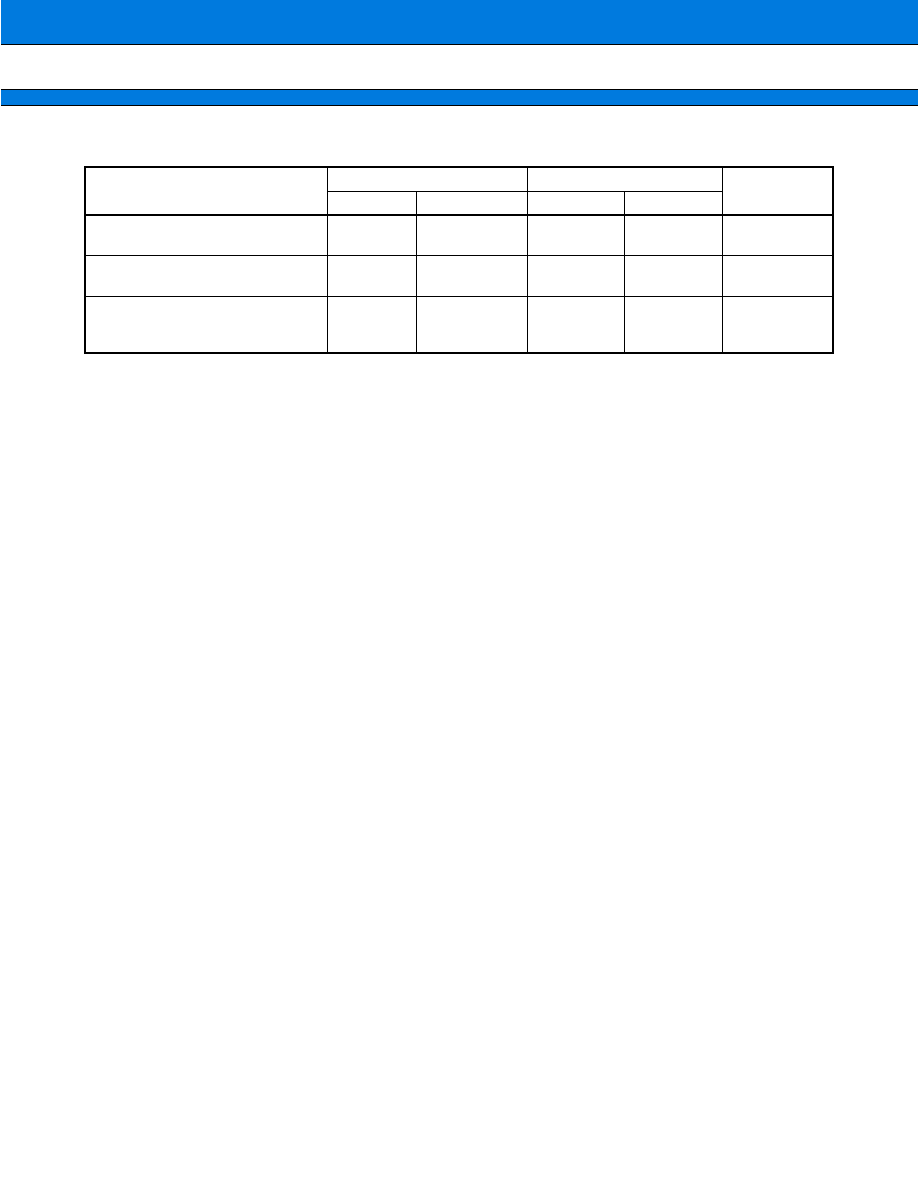
MB91106 Series
36
(Continued)
* : When using in REALOS/FR, interrupt 0x40, 0x41 for system code.
Interrupt causes
Interrupt number
Interrupt level
TBR default
address
Decimal
Hexadecimal
Register
Offset
Reserved for system (used in
REALOS*)
64
40
--
2FC
H
000FFEFC
H
Reserved for system (used in
REALOS*)
65
41
--
2F8
H
000FFEF8
H
Used in INT instructions
66
to
255
42
to
FF
--
2F4
H
to
000
H
000FFEF4
H
to
000FFD00
H
37
MB91106 Series
s
PERIPHERAL RESOURCES
1.
I/O Ports
There are 2 types of I/O port register structure; port data register (PDR0 to PDRF) and data direction register
(DDR0 to DDRF), where bits PDR0 to PDRF and bits DDR0 to DDRF corresponds respectively. Each bit on
the register corresponds to an external pin. In port registers input/output register of the port configures input/
output function of the port, while corresponding bit (pin) configures input/output function in data direction
registers. Bit "0" specifies input and "1" specifies output.
∑ For input (DDR = "0") setting;
PDR reading operation: reads level of corresponding external pin.
PDR writing operation: writes set value to PDR.
∑ For output (DDR = "1") setting;
PDR reading operation: reads PDR value.
PDR writing operation: outputs PDR value to corresponding external pin.
(1) Register configuration
∑ Port data register
bit 7
bit 0
000001
H
000000
H
000007
H
000006
H
000005
H
000004
H
00000B
H
000009
H
000008
H
000012
H
000013
H
X X X X X X X X
B
X X X X X X X X
B
X X X X X X X X
B
X X X X X X X X
B
X X X X X X X X
B
- - - - - - - X
B
- - X X X X X X
B
- X X X X X X X
B
X X X X X X X X
B
X X X X X X X X
B
X X X X X X X X
B
Address
Initial value
: Access
: Readable and writable
: Indeterminate
(R/W)
(R/W)
(R/W)
(R/W)
(R/W)
(R/W)
(R/W)
(R/W)
(R/W)
(R/W)
(R/W)
( )
R/W
X
PDR2
PDR3
PDR4
PDR5
PDR6
PDR7
PDR8
PDRA
PDRB
PDRE
PDRF
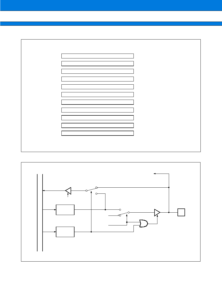
MB91106 Series
38
(2) Block diagram
( )
W
≠
∑ Data direction register
: Access
: Write only
: Unused
bit 7
bit 0
000601
H
000600
H
000607
H
000606
H
000605
H
000604
H
00060B
H
000609
H
000608
H
0000D2
H
0000D3
H
0 0 0 0 0 0 0 0
B
0 0 0 0 0 0 0 0
B
0 0 0 0 0 0 0 0
B
0 0 0 0 0 0 0 0
B
0 0 0 0 0 0 0 0
B
- - - - - - - 0
B
- - 0 0 0 0 0 0
B
- 0 0 0 0 0 0 0
B
0 0 0 0 0 0 0 0
B
0 0 0 0 0 0 0 0
B
0 0 0 0 0 0 0 0
B
Address
Initial value
(W)
(W)
(W)
(W)
(W)
(W)
(W)
(W)
(W)
(W)
(W)
DDR2
DDR3
DDR4
DDR5
DDR6
DDR7
DDR8
DDRA
DDRB
DDRE
DDRF
PDR read
PDR
(Port data register)
DDR
(Data direction register)
Data b
u
s
Resource input
0
1
0
1
Resource output
Resource output enable
Pin

39
MB91106 Series
2.
DMA Controller (DMAC)
The DMA controller is a module embedded in FR family devices, and performs DMA (direct memory access)
transfer.
DMA transfer performed by the DMA controller transfers data without intervention of CPU, contributing to
enhanced performance of the system.
∑ 8 channels
∑ Mode: single/block transfer, burst transfer and continuous transfer: 3 kinds of transfer
∑ Transfer all through the area
∑ Max. 65536 of transfer cycles
∑ Interrupt function right after the transfer
∑ Selectable for address transfer increase/decrease by the software
∑ External transfer request input pin, external transfer request accept output pin, external transfer complete
output pin three pins for each
(1) Registers configuration
∑ DMAC internal registers
bit 31
bit 0
Address
00000200
H
X X X X X X X X
B
X X X X X X X X
B
X X X X X X X X
B
X 0 0 0 0 0 0 0
B
Initial value
: Access
: Readable and writable
: Indeterminate
DPDP
( )
R/W
X
DACSR
DATCR
(R/W)
(R/W)
(R/W)
∑ DMAC parameter descriptor pointer
∑ DMAC control status register
∑ DMAC pin control register
bit 31
bit 0
bit 31
bit 0
Address
00000208
H
0 0 0 0 0 0 0 0
B
0 0 0 0 0 0 0 0
B
0 0 0 0 0 0 0 0
B
0 0 0 0 0 0 0 0
B
Initial value
X X X X X X X X
B
X X 0 0 0 0 0 0
B
X X 0 0 0 0 0 0
B
X X 0 0 0 0 0 0
B
Initial value
Address
00000204
H
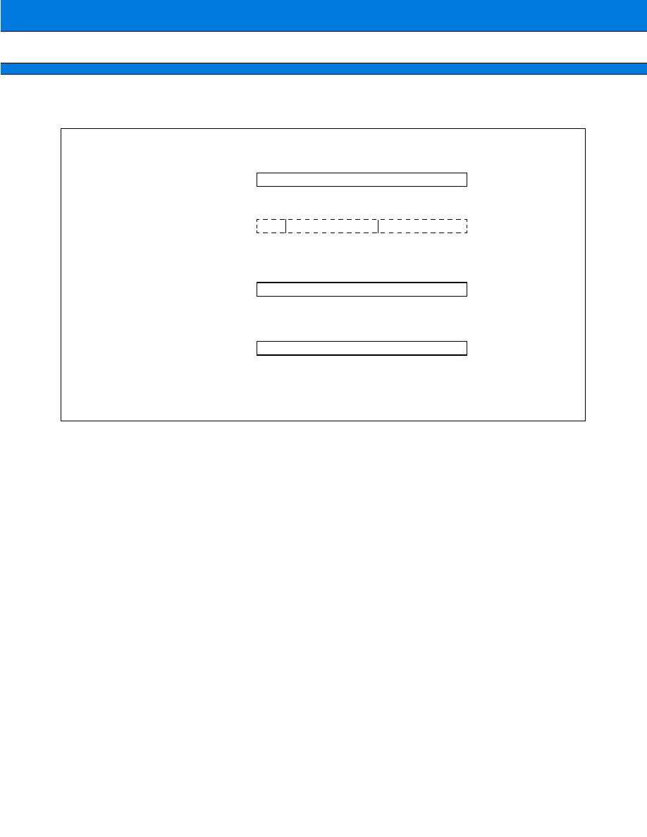
MB91106 Series
40
∑ DMAC descriptor
bit 31
bit 16
(R/W)
∑ The first word of descriptor
bit 15
bit 0
(R/W)
bit 31
bit 0
(R/W)
bit 31
bit 0
(R/W)
∑ The second word of descriptor
∑ The third word of descriptor
bit 11
bit 8 bit 7
DMACT
SADR
DADR
BLK
≠
R/W: Readable and writable
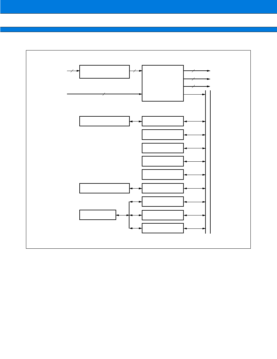
41
MB91106 Series
(2) Block diagram
DREQ0 to DREQ2
Inner resource
Transfer request
Edge/level
detection circuit
Data buffer
BLK DEC
INC / DEC
3
3
5
Sequencer
Switcher
DMAC parameter descriptor pointer
(DPDP)
DMAC control status registger
(DACSR)
DMAC pin control registger
(DATCR)
Mode
BLK
The first word of descriptor
(DMACT)
The second word of descriptor
(SADR)
The third word of descriptor
(DADR)
DACK0 to DACK2
EOP0 to EOP2
Interrupt request
3
8
3
Data b
u
s
MB91106 Series
42
3.
UART
The UART is a serial I/O port for supporting asynchronous (start-stop system) communication or CLK
synchronous communication, and it has the following features.
The MB91106 consists of 3 channels of UART.
∑ Full double double buffer
∑ Both a synchronous (start-stop system) communication and CLK synchronous communication are available.
∑ Supporting multi-processor mode
∑ Perfect programmable baud rate
Any baud rate can be set by internal timer (refer to section "4. U-TIMER").
∑ Any baud rate can be set by external clock.
∑ Error checking function (parity, framing and overrun)
∑ Transfer signal: NRZ code
∑ Enable DMA transfer/start by interrupt.
(1) Register configuration
∑ Serial control register 0 to 2
Initial value
0 0 0 0 0 1 0 0
B
bit 15
bit 0
bit 8 bit 7
SCR0 to SCR2
SMR
(R/W)
Address
∑ Serial model register 0 to 2
Initial value
0 0 - - 0 - 0 0
B
bit 15
bit 0
bit 8 bit 7
(SCR)
SMR0 to SMR2
(R/W)
SMR0 : 00001F
H
SMR1 : 000023
H
SMR2 : 000027
H
∑ Serial status register 0 to 2
Initial value
0 0 0 0 1 - 0 0
B
bit 15
bit 0
bit 8 bit 7
SSR0 to SSR2
SID
(R/W)
SSR0 : 00001C
H
SSR1 : 000020
H
SSR2 : 000024
H
∑ Serial input data register 0 to 2
Initial value
X X X X X X X X
B
bit 15
bit 0
bit 8 bit 7
(SSR)
SIDR0 to SIDR2
(R)
: Access
: Readable and writable
: Unused
: Indeterminate
( )
R/W
≠
X
SCR0 : 00001E
H
SCR1 : 000022
H
SCR2 : 000026
H
Address
Address
SIDR0 : 00001D
H
SIDR1 : 000021
H
SIDR2 : 000025
H
Address
∑ Serial output data register 0 to 2
Initial value
X X X X X X X X
B
bit 15
bit 0
bit 8 bit 7
(SSR)
SODR0 to SODR2
(W)
SODR0 : 00001D
H
SODR1 : 000021
H
SODR2 : 000025
H
Address
43
MB91106 Series
(2) Block diagram
Control signals
From U-TIMER
From external clock
SC
SI
(receive data)
Clock select
circuit
Receive clock
Transmit clock
Receive interrupt
(to CPU)
SC (clock)
Transmit interrupt
(to CPU)
Receive control circuit
Start bit detect
circuit
Receive bit counter
Receive parity
counter
Transmit control circuit
Transmit start
circuit
Transmit bit counter
Transmit parity
counter
SO (transmit data)
Receive status
judge circuit
Receive error
generate signal
for DMA
(to DMAC)
Receive shifter
Serial input data register
SIDR
Receive
complete
Transmit shifter
Serial output data register
SIDR
Transmit
start
R-bus
Serial register
(SMR)
MD1
MD0
CS0
SCKE
SOE
Serial control
register
(SCR)
PEN
P
SBL
CL
A/D
REC
RXE
TXE
Serial status
register
(SSR)
PE
ORE
FRE
RDRF
TDRE
RIE
TIE
Control signals
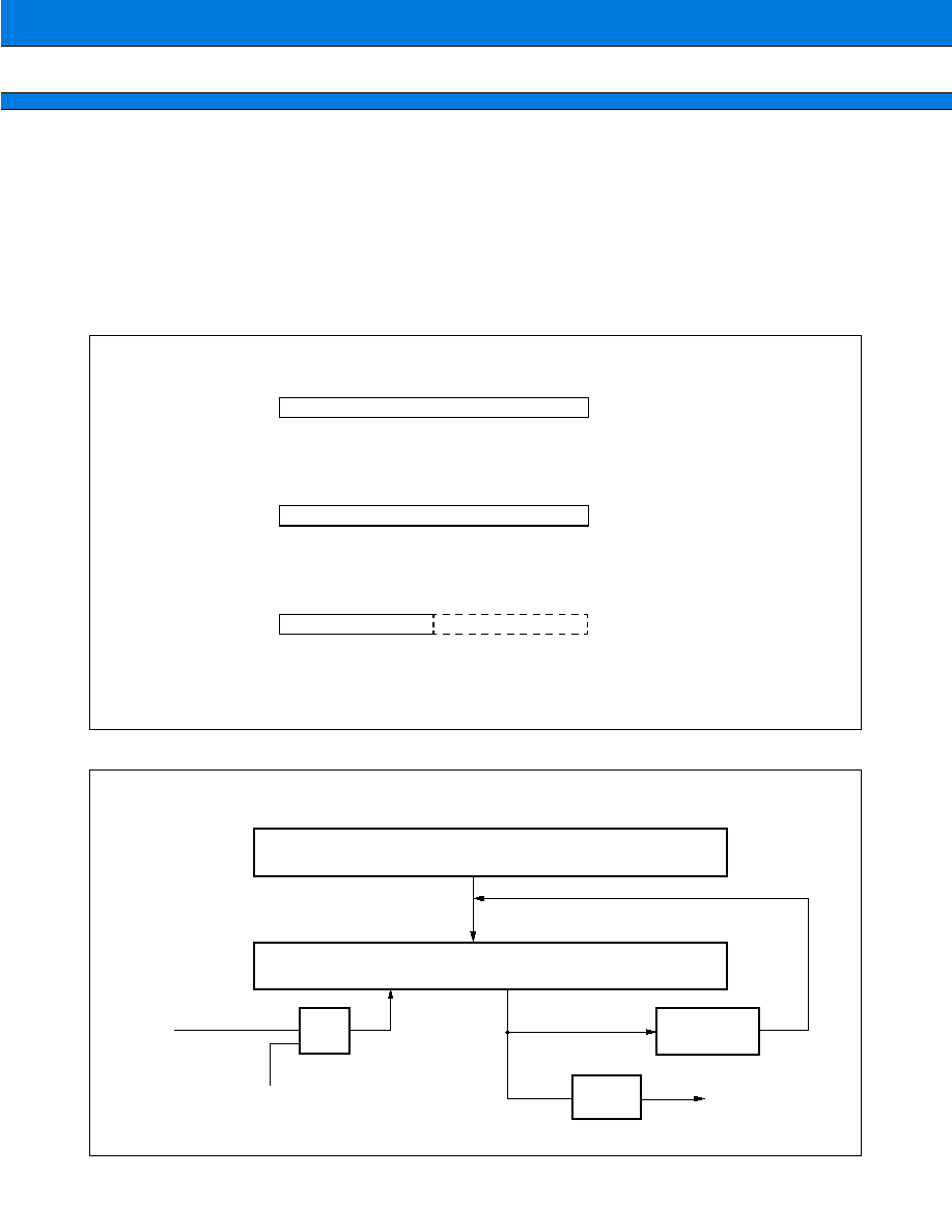
MB91106 Series
44
4.
U-TIMER (16-bit Timer for UART Baud Rate Generation)
The U-TIMER is a 16-bit timer for generating UART baud rate. Combination of chip operating frequency and
reload value of U-TIMER allows flexible setting of baud rate.
The U-TIMER operates as an interval timer by using interrupt issued on counter underflow.
The MB91106 has 3 channel U-TIMER embedded on the chip. When used as an interval timer, two cupple of
U-TIMER (ch0, ch1) can be cascaded and an interva of up to 2
32
◊
can be counted.
(1) Register configuration
(2) Block diagram
∑ U-TIMER register ch.0 to ch.2
Initial value
0 0 0 0 0 0 0 0
0 0 0 0 0 0 0 0
B
B
bit 15
bit 0
UTIM0 to UTIM2
(R)
UTIM0 : 00000078
H
UTIM1 : 0000007C
H
UTIM2 : 00000080
H
Address
∑ U-TIMER reload register ch.0 to ch.2
Initial value
0 0 0 0 0 0 0 0
0 0 0 0 0 0 0 0
B
B
bit 15
bit 0
UTIMR0 to UTIMR2
(W)
UTIMR0 : 00000078
H
UTIMR1 : 0000007C
H
UTIMR2 : 00000080
H
Address
∑ U-TIMER control register ch.0 to ch.2
bit 15
bit 0
UTIMC0 to UTIMC2
: Access
: Readable and writable
: Unused
( )
R/W
≠
UTIMC0 : 0000007B
H
UTIMC1 : 0000007F
H
UTIMC2 : 00000083
H
Address
(Vacancy)
bit 8 bit 7
Initial value
0 - - 0 0 0 0 1
B
(R/W)
bit 15
bit 0
Reload register (U-TIMER)
bit 15
bit 0
U-TIMER register (UTIM)
Load
(Peripheral clock)
MUX
(ch.0 only)
Underflow
U-TIMER
Clock
Underflow
U-TIMER control register
(UTIMC)
f.f.
To UART

45
MB91106 Series
5.
PWM Timer
The PWM timer can output high accurate PWM waves efficiently.
MB91106 has inner 4-channel PWM timers, and has the following features.
∑ Each channel consists of a 16-bit down counter, a 16-bit data resister with a buffer for scyde setting, a 16-
bit compare resister with a buffer for duty setting, and a pin controller.
∑ The count clock of a 16-bit down counter can be selected from the following four inner clocks.
Inner clock
,
/4,
/16,
/64
∑ The counter value can be initialized "FFFF
H
" by the resetting or the counter borrow.
∑ PWM output (each channel)
MB91106 Series
46
(1) Register configuration
bit 15
bit 0
bit 8 bit 7
(Vacancy)
GCN2
: Access
: Readable and writable
: Read only
: Write only
: Unused
: Indeterminate
( )
R/W
R
W
≠
X
∑ Control status register H0 to 3
Initial value
0 0 0 0 0 0 0 -
B
bit 15
bit 0
bit 8 bit 7
PCNH0 to PCNH3
(PCNL)
(R/W)
Address
PCNH0 : 0000E6
H
PCNH1 : 0000EE
H
PCNH2 : 0000F6
H
PCNH3 : 0000FE
H
∑ Control status register L0 to 3
Initial value
0 0 0 0 0 0 0 0
B
bit 15
bit 0
(PCNH)
PCNL0 to PCNL3
(R/W)
Address
PCNL0 : 0000E7
H
PCNL1 : 0000EF
H
PCNL2 : 0000F7
H
PCNL3 : 0000FF
H
∑ PWM cycle setting register 0 to 3
Initial value
X X X X X X X X
B
bit 15
bit 0
PCSR0 to PCSR3
(W)
Address
PCSR0 : 0000E2
H
PCSR1 : 0000EA
H
PCSR2 : 0000F2
H
PCSR3 : 0000FA
H
∑ PWM duty setting register 0 to 3
bit 15
bit 0
PDUT0 to PDUT3
Address
PDUT0 : 0000E4
H
PDUT1 : 0000EC
H
PDUT2 : 0000F4
H
PDUT3 : 0000FC
H
Initial value
X X X X X X X X
X X X X X X X X
B
B
(W)
∑ PWM timer register 0 to 3
bit 15
bit 0
PTMR0 to PTMR3
Address
PTMR0 : 0000E0
H
PTMR1 : 0000E8
H
PTMR2 : 0000F0
H
PTMR3 : 0000F8
H
Initial value
1 1 1 1 1 1 1 1
1 1 1 1 1 1 1 1
B
B
(R)
∑ General control register 1, 2
bit 15
bit 0
GCN1
Address
GCN1 : 0000DC
H
Initial value
0 0 1 1 0 0 1 0
0 0 0 1 0 0 0 0
B
B
(R/W)
Address
GCN1 : 0000DF
H
Initial value
0 0 0 0 0 0 0 0
B
(R/W)
47
MB91106 Series
(2) Block diagram
∑ Block diagram (general construction)
∑ Block diagram (for one channel)
16-bit reload timer
ch.0
16-bit reload timer
ch.1
General control
register 2
External TRG0 to TRG3
4
4
General control
register 1
(cause selection)
TRG input
PWM timer ch.0
TRG input
PWM timer ch.1
TRG input
PWM timer ch.2
TRG input
PWM timer ch.3
PWM0
PWM1
PWM2
PWM3
Prescaler
1 / 1
1 / 4
1 / 16
1 / 64
PWM cycle
setting register
(PCSR)
PWM duty
setting register
(PDUT)
ck
Load
16-bit down counter
Start
Borrow
cmp
Peripheral clock
TRG input
Enable
Edge detect
Soft trigger
PPG mask
Reverse bit
PWM output
IRQ
S
Q
R
Interr
upt
selection

MB91106 Series
48
6.
16-bit Reload Timer
The 16-bit reload timer consists of a 16-bit down counter, a 16-bit reload timer, a prescaler for generating
internal count clock and control registers.
Internal clock can be selected from 3 types of internal clocks (divided by 2/8/32 of machine clock).
The DMA transfer can be started by the interruption.
The MB91106 consists of 3 channels of the 16-bit reload timer.
(1) Register configuration
∑ 16-bit reload timer control status register 0 to 2
Initial value
- - - - 0 0 0 0
0 0 0 0 0 0 0 0
B
B
bit 15
bit 0
TMCSR0 to TMCSR2
(R/W)
TMCSR0 : 00002E
H
TMCSR1 : 000036
H
TMCSR2 : 000042
H
Address
∑ 16-bit timer register 0 to 2
bit 15
bit 0
TMR0 to TMR2
TMR0 : 00002A
H
TMR1 : 000032
H
TMR2 : 00003E
H
Address
∑ 16-bit reload register 0 to 2
bit 15
bit 0
TMRLR0 to TMRLR2
TMRLR0 : 000028
H
TMRLR1 : 000030
H
TMRLR2 : 00003C
H
Address
Initial value
X X X X X X X X
X X X X X X X X
B
B
(R)
Initial value
X X X X X X X X
X X X X X X X X
B
B
(W)
: Access
: Readable and writable
: Read Only
: Write Only
: Unused
: Indeterminate
( )
R/W
R
W
≠
X
49
MB91106 Series
(2) Block diagram
Clock selector
R-
b
u
s
Internal clock
16-bit reload register (TMRLR)
2
3
2
2
3
8
16
16
16-bit down counter UF
PWM (ch.0, ch.1)
A/D (ch.2)
IRQ
Reload
EXCK
Retrigger
IN CTL.
OUT
CTL.
RELD
MOD2
Prescaler
clear
MOD1
MOD0
GATE
2
1
2
3
2
5
CSL1
CSL0
OUTE
OUTL
INTE
UF
CNTE
TRG
MB91106 Series
50
7.
Bit Search Module
The bit search module detects transitions of data (0 to 1/1 to 0) on the data written on the input registers and
returns locations of the transitions.
(1) Register configuration
(2) Block diagram
: Access
: Readable and writable
: Read only
: Write only
: Indeterminate
( )
R/W
R
W
X
∑ Bit search module 0, 1-detection data register
bit 31
bit 0
BSD0, BSD1
BSD0 : 000003F0
H
BSD1 : 000003F4
H
Address
Initial value
X X X X X X X X
X X X X X X X X
X X X X X X X X
X X X X X X X X
B
B
B
B
(R/W)
∑ Bit search module transition-detection data register
bit 31
bit 0
BSDC
000003F8
H
Address
Initial value
X X X X X X X X
X X X X X X X X
X X X X X X X X
X X X X X X X X
B
B
B
B
(W)
∑ Bit search module detection result register
bit 31
bit 0
BSRR
Address
Initial value
X X X X X X X X
X X X X X X X X
X X X X X X X X
X X X X X X X X
B
B
B
B
(R)
000003FC
H
D-b
u
s
Input latch
Address
decoder
Single-detection data recovery
Search result register (BSRR)
Bit search circuit
Detection
mode

51
MB91106 Series
8.
10-bit A/D Converter (Successive Approximation Conversion Type)
The A/D converter is the module which converts an analog input voltage to a digital value, and it has following
features.
∑ Minimum converting time: 5.6
µ
s/ch. (system clock: 25 MHz)
∑ Inner sample and hold circuit
∑ Resolution: 10 bits
∑ Analog input can be selected from 4 channels by program.
Single convert mode: 1 channel is selected and converted.
Scan convert mode: Converting continuous channels. Maximum 4 channels are programmable.
Continuous convert mode: Converting the specified channel repeatedly.
Stop convert mode: After converting one channel then stop and wait till next activation synchronising at
the beginning of conversion can be peformed.
∑ DMA transfer operation is available by interruption.
∑ Operating factor can be selected from the software, the external trigger (falling edge), and 16-bit reroad timer
(rising edge).
(1) Register configuration
: Access
: Readable and writable
: Read only
: Unused
: Indeterminate
( )
R/W
R
≠
X
∑ A/D converter control status register
bit 15
bit 0
ADCS
Address
0000003A
H
Initial value
0 0 0 0 0 0 0 0
0 0 0 0 0 0 0 0
B
B
(R/W)
∑ A/D converter data register
bit 15
bit 0
ADCR
Address
00000038
H
Initial value
0 0 0 0 0 0 X X
X X X X X X X X
B
B
(R)
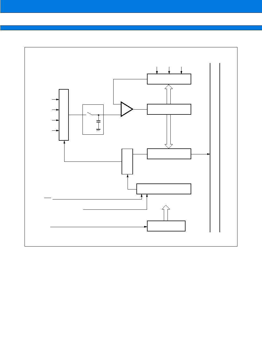
MB91106 Series
52
(2) Block diagram
R-b
u
s
TIM0
(internal connection)
(16-bit reload timer 2)
Sample & hold circuit
ATG
Timer start
Trigger start
Comparator
Internal voltage generator
Successive approximation
register
A/D Converter Data register
(ADCR)
A/D Converter control status
register (ADCS)
Prescaler
Decoder
Input circuit
AN0
AN1
AN2
AN3
MPX
AV
CC
AV
SS
AVR
Operating clock
(Peripheral clock)

53
MB91106 Series
9.
Interrupt Controller
The interrupt controller processes interrupt acknowledgments and arbitration between interrupts.
∑ Hardware Configuration
Interrupt controller is configured by ICR resistor, interrupt priority decision circuit, interrupt level, vector
generation and HLDREQ cancel request, and has the following functions.
∑ Main Functions
NMI request/Interrupt request detection
Priority (judgement) decision (via level and vector)
Transfer of judged interrupt level to CPU
Transfer of judged interrupt vector to CPU
Return instruction from the stop mode via NMI/interrupt
Generation of HOLD request cancel request to the bus timer
MB91106 Series
54
(1) Register configuration
ICR00
ICR01
ICR02
ICR03
ICR04
ICR05
ICR06
ICR07
ICR08
ICR09
ICR10
ICR11
ICR12
ICR13
ICR14
ICR15
ICR16
bit 7
bit 0
00000400
H
00000401
H
00000402
H
00000403
H
00000404
H
00000405
H
00000406
H
00000407
H
00000408
H
00000409
H
0000040A
H
0000040B
H
0000040C
H
0000040D
H
0000040E
H
0000040F
H
00000410
H
- - - 11111
B
(R/W)
- - - 11111
B
(R/W)
- - - 11111
B
(R/W)
- - - 11111
B
(R/W)
- - - 11111
B
(R/W)
- - - 11111
B
(R/W)
- - - 11111
B
(R/W)
- - - 11111
B
(R/W)
- - - 11111
B
(R/W)
- - - 11111
B
(R/W)
- - - 11111
B
(R/W)
- - - 11111
B
(R/W)
- - - 11111
B
(R/W)
- - - 11111
B
(R/W)
- - - 11111
B
(R/W)
- - - 11111
B
(R/W)
- - - 11111
B
(R/W)
Address
Initial value
ICR17
ICR18
ICR19
ICR20
ICR21
ICR22
ICR23
ICR24
ICR25
ICR26
ICR27
ICR28
ICR29
ICR30
ICR31
ICR47
bit 7
bit 0
00000411
H
00000412
H
00000413
H
00000414
H
00000415
H
00000416
H
00000417
H
00000418
H
00000419
H
0000041A
H
0000041B
H
0000041C
H
0000041D
H
0000041E
H
0000041F
H
0000042F
H
- - - 11111
B
(R/W)
- - - 11111
B
(R/W)
- - - 11111
B
(R/W)
- - - 11111
B
(R/W)
- - - 11111
B
(R/W)
- - - 11111
B
(R/W)
- - - 11111
B
(R/W)
- - - 11111
B
(R/W)
- - - 11111
B
(R/W)
- - - 11111
B
(R/W)
- - - 11111
B
(R/W)
- - - 11111
B
(R/W)
- - - 11111
B
(R/W)
- - - 11111
B
(R/W)
- - - 11111
B
(R/W)
- - - 11111
B
(R/W)
Address
Initial value
: Access
: Redable and writable
: Unused
( )
R/W
≠
∑ Hold request cancel request level setting register
bit 7
bit 0
HRCL
Address
00000431
H
Initial value
- - - 1 1 1 1 1
B
(R/W)
∑ Interrupt control register 0 to 31, 47
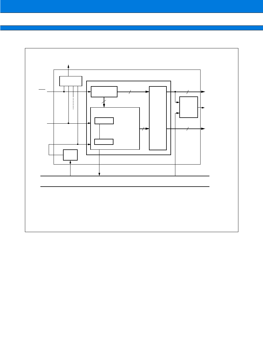
55
MB91106 Series
(2) Block diagram
*1: DLYI stands for delayed interrupt module (delayed interrupt generation block) (refer to the section "11. Delayed Interrupt
Module" for detail).
*2: INT0 is a wake-up signal to clock control block in the sleep or stop status.
*3: HLDCAN is a bus release request signal for bus masters other than CPU.
*4: LEVEL5 to LEVEL0 are interrupt level outputs.
*5: VCT5 to VCT0 are interrupt vector outputs.
R-bus
NMI processing
Priority judgment
LEVEL4 to
LEVEL0*
4
VCT5 to
VCT0*
5
HLDCAN*
3
OR
ICR47
ICR00
Vector judgment
5
5
6
6
4
∑
RI00
RI47
∑
∑
∑
∑
∑
∑
∑
(DLYIRQ)
NMI
HLDREQ
cancel
request
Level,
vector
generation
Level judgment
DLYI*
1
INT0*
2
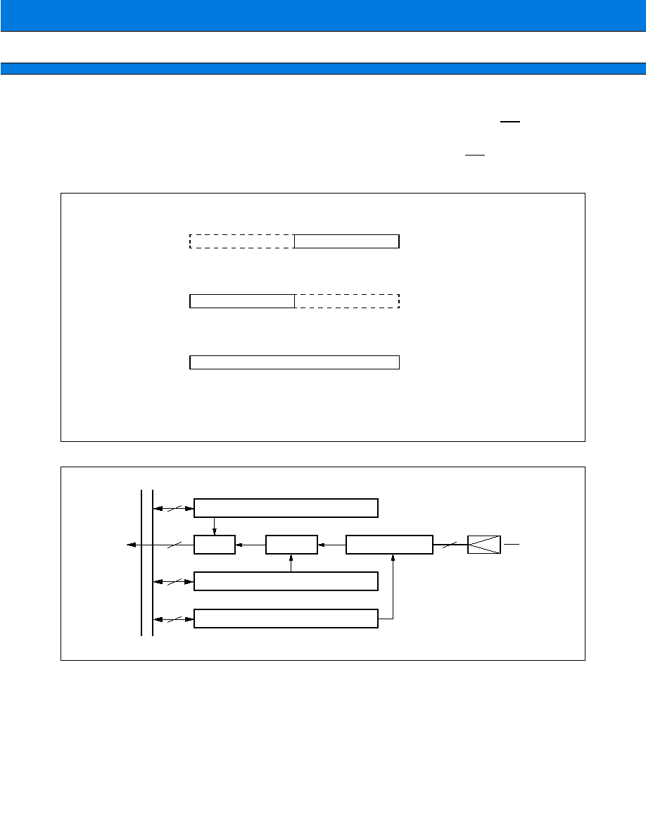
MB91106 Series
56
10. External Interrupt/NMI Control Block
The external interrupt/NMI control block controls external interrupt request signals input to NMI pin and INT0
to INT3 pins.
Detecting levels can be selected from "H", "L", rising edge and falling edge (not for NMI pin).
(1) Register configuration
(2) Block diagram
: Access
: Redable and writable
( )
R/W
∑ Interrupt enable register
bit 15
bit 0
(EIRR)
Address
00000095
H
Initial value
0 0 0 0 0 0 0 0
B
(R/W)
ENIR
∑ External interrupt cause register
bit 15
bit 0
EIRR
Address
00000094
H
(ENIR)
∑ External interrupt request level setting register
bit 15
bit 0
ELVR
Address
00000099
H
bit 7
bit 8
Initial value
0 0 0 0 0 0 0 0
B
(R/W)
Initial value
0 0 0 0 0 0 0 0
B
(R/W)
Interrupt enable register (ENIR)
R-b
u
s
Interrupt
request
External interrupt cause register (EIRR)
External interrupt request level setting register (ELVR)
Gate
Cause F/F
Edge detection circuit
INT0 to INT3
NMI
9
8
8
8
5

57
MB91106 Series
11. Delayed Interrupt Module
Delayed interrupt module is a module which generates a interrupt for changing a task. By using this delayed
interrupt module, an interrupt request to CPU can be generated/cancelled by the software.
Refer to the section "9. Interrupt Controller" for delayed interrupt module block diagram.
∑ Register configuration
bit 7
bit 0
Address
DICR
00000430
H
: Access
: Redable and writable
: Unused
( )
R/W
≠
∑ Delayed interrupt control register
Initial value
- - - - - - - 0
B
(R/W)

MB91106 Series
58
12. Clock Generation (Low-power consumption mechanism)
The clock control block is a module which undertakes the following functions.
∑ CPU clock generation (including gear function)
∑ Peripheral clock generation (including gear function)
∑ Reset generation and cause hold
∑ Standby function
∑ DMA request prohibit
∑ PLL (multiplier circuit) embedded
(1) Register configuration
∑ Reset cause register/watchdog cycle control register
bit 15
bit 0
RSRR
Address
00000480
H
Initial value
1 X X X X - 0 0
B
(R/W)
(STCR)
∑ Standby control register
bit 15
bit 0
(RSRR/WTCR)
Address
00000481
H
(STCR)
bit 9 bit 8
bit 7
Initial value
0 0 0 1 1 1 - -
B
(R/W)
∑ DMA controller request squelch register
bit 15
bit 0
PDRR
Address
00000482
H
(CTBR)
bit 8
Initial value
- - - - 0 0 0 0
B
(R/W)
bit 10
WTCR
∑ Timebase timer clear register
bit 15
bit 0
(PDRR)
Address
00000483
H
CTBR
bit 7
∑ Gear control register
bit 15
bit 0
GCR
Address
00000484
H
(WPR)
bit 8
Initial value
X X X X X X X X
B
(W)
Initial value
1 1 0 0 1 1 - 1
B
(R/W)
∑ Watchdog reset occurrence postpone register
bit 15
bit 0
(GCR)
Address
00000485
H
WPR
bit 7
Initial value
X X X X X X X X
B
(W)
∑ PLL control register
bit 15
bit 0
PCTR
Address
00000488
H
(Vacancy)
bit 8
Initial value
0 0 - - 0 - - -
B
(R/W)
: Access
: Readable and writable
: Read Only
: Write Only
: Unused
: Indeterminate
( )
R/W
R
W
≠
X
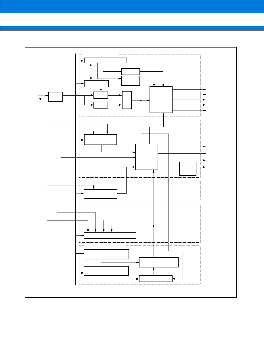
59
MB91106 Series
(2) Block diagram
[Gear control block]
CPU clock
Gear control register (GCR)
Internal bus clock
External bus clock
Peripheral
DMA clock
Internal
peripheral clock
CPU gear
Internal clock
generation
circuit
Peripheral
gear
PLL control register
(PCTR)
PLL
1/2
Selection
circuit
R-b
u
s
Oscillator
circuit
X0
X1
STOP state
SLEEP state
CPU hold request
Internal reset
Status
transition
control circuit
Reset
generation
F/F
Standby control
register (STCR)
[DMA prohibit circuit]
[Stop/sleep control block]
DMA request prohibit
register (PDRR)
Reset cause register (RSRR)
[Reset cause circuit]
[Watchdog control block]
Watchdog reset generation
postpone register (WPR)
Timebase timer clear
register (CTBR)
Watchdog reset
postpone register F/F
Timebase time
Count clock
Internal
interrupt request
Internal reset
CPU hold enable
DMA
request
Power on sel
RST pin

MB91106 Series
60
13. External Bus Interface
The external bus interface controls the interface between the device and the external memory and also the
external I/O, and has the following features.
∑ 25-bit (32 Mbytes) address output
∑ 6 independent banks owing to the chip select function.
Can be set to anywhere on the logical address space for minimum unit 64 Kbytes.
Total 32 Mbytes
◊
6 area setting is available by the address pin and the chip select pin.
∑ 8/16-bit bus width setting are available for every chip select area.
∑ Programmable automatic memory wait (max. for 7 cycles) can be inserted.
∑ DRAM interface support
Three kinds of DRAM interface: Double CAS DRAM (normally DRAM I/F)
Single CAS DRAM
Hyper DRAM
2 banks independent control (RAS, CAS, etc. control signals)
DRAM select is available from 2CAS/1WE and 1CAS/2WE.
Hi-speed page mode supported
CBR/self refresh supported
Programmable wave form
∑ Unused address/data pin can be used for I/O port.
∑ Little endian mode supported
∑ Clock doublure: Internal bus 50 MHz, external bus 25 MHz (at source oscillation 12.5 MHz)
61
MB91106 Series
(1) Register configuration
: Access
: Redable and writable
: Write only
: Unused
: Indeterminate
( )
R/W
W
≠
X
∑ Area select register 1 to 5
bit 15
bit 0
ASR1
Address
0000060C
H
Initial value
0 0 0 0 0 0 0 0
0 0 0 0 0 0 0 1
B
B
ASR2
00000610
H
0 0 0 0 0 0 0 0
0 0 0 0 0 0 0 2
B
B
ASR3
00000614
H
0 0 0 0 0 0 0 0
0 0 0 0 0 0 0 3
B
B
ASR4
00000618
H
0 0 0 0 0 0 0 0
0 0 0 0 0 0 0 4
B
B
ASR5
0000061C
H
0 0 0 0 0 0 0 0
0 0 0 0 0 0 0 5
B
B
Initial value
0 0 0 0 0 0 0 0
0 0 0 0 0 0 0 0
B
B
(W)
bit 15
bit 0
AMR1 to AMR5
Address
AMR1 : 0000060E
H
AMR2 : 00000612
H
AMR3 : 00000616
H
AMR4 : 0000061A
H
AMR5 : 0000061E
H
∑ Area mask register 1 to 5
bit 15
bit 0
bit 8 bit 7
AMD0
AMD1
bit 15
bit 0
bit 8 bit 7
(AMD5)
DSCR
∑ Area mode register 0, 1, 32, 4, 5
Initial value
- - - 0 0 1 1 1
0 - - 0 0 0 0 0
B
B
(R/W)
AMD0 : 00000620
H
AMD1 : 00000621
H
Address
AMD32
AMD4
AMD32 : 00000622
H
AMD4 : 00000623
H
0 0 0 0 0 0 0 0
0 - - 0 0 0 0 0
B
B
AMD5
(DSCR)
AMD5 : 00000624
H
∑ DRAM signle control register
Address
00000625
H
Initial value
0 0 0 0 0 0 0 0
B
(W)
bit 15
bit 0
RFCR
∑ Refresh control register
Address
00000626
H
Initial value
- - X X X X X X
0 0 - - - 0 0 0
B
B
(R/W)
bit 15
bit 0
EPCR0
∑ External pin control register 0, 1
Address
EPCR0 : 00000628
H
Initial value
- - - - 1 1 0 0
- 1 1 1 1 1 1 1
B
B
(W)
bit 15
bit 0
DMCR4, DMCR5
Address
DMCR4 : 0000062C
H
DMCR5 : 0000062E
H
EPCR1
- - - - - - - 1
1 1 1 1 1 1 1 1
B
B
EPCR1 : 0000062A
H
∑ DRAM control register 4, 5
bit 15
bit 0
bit 8 bit 7
LER
(MODR)
Address
000007FE
H
∑ Litter endian register
bit 15
bit 0
bit 8 bit 7
(LER)
MODR
Address
000007FF
H
∑ Mode register
Initial value
0 0 0 0 0 0 0 0
0 0 0 0 0 0 0 -
B
B
(R/W)
Initial value
- - - - - 0 0 0
B
(W)
Initial value
X X X X X X X X
B
(W)
0 - - 0 0 0 0 0
B
(R/W)
(R/W)
(W)
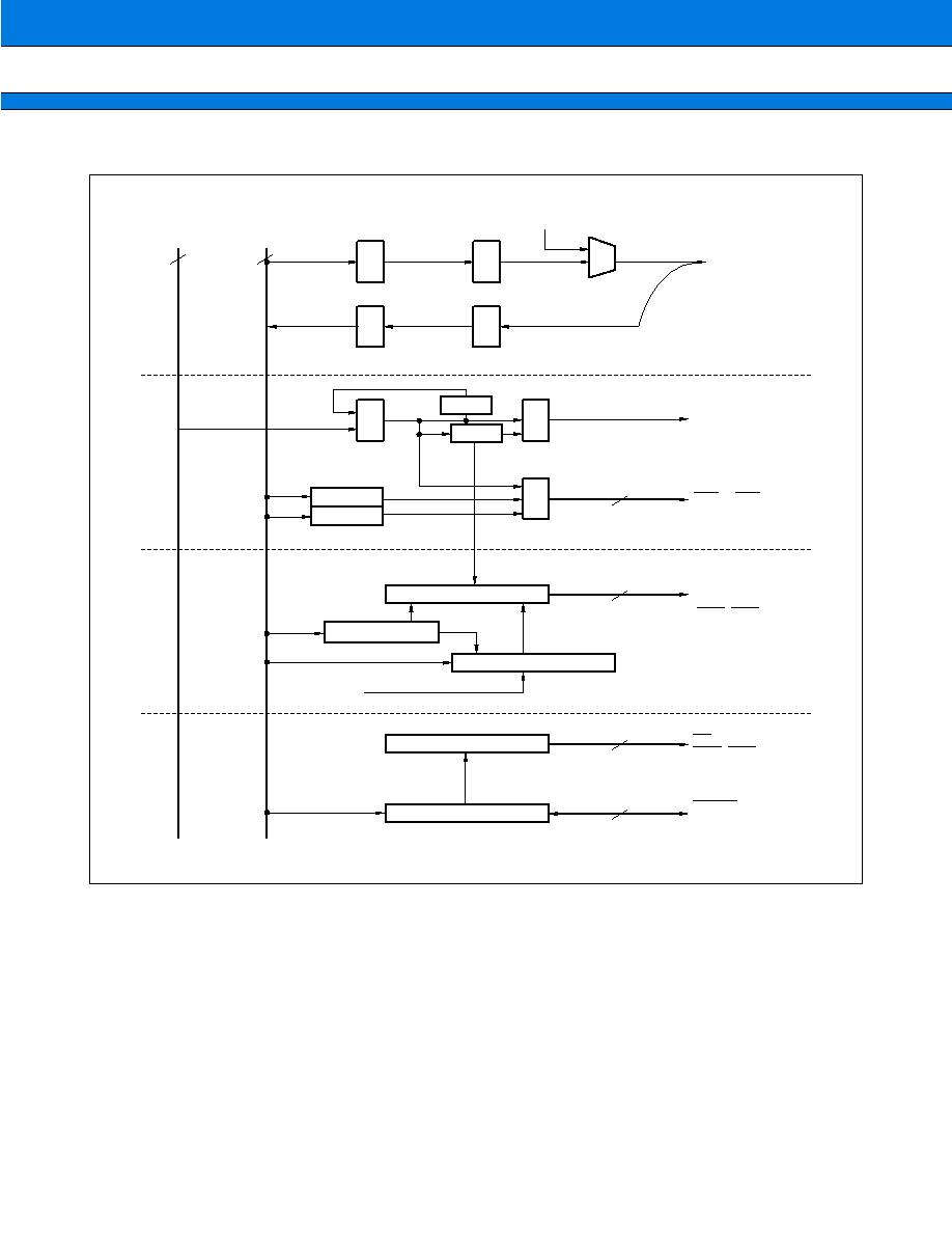
MB91106 Series
62
(2) Block diagram
Address bus
32
Data bus
32
MUX
Read buffer
Switch
Switch
Write buffer
Write buffer
A-OUT
Address buffer
+1 or +2
Inpage
Shifter
Comparator
DRAM control
Underflow
All blocks control
To TBT
Refresh counter register (RFCR)
DRAM control register (DMCR)
Area select
register(ASR)
DATA BLOCK
ADDRESS BLOCK
External data bus
External address bus
CS0 to CS5
RAS0, RAS1
CS0L, CS1L
CS0H, CS1H
DW0, DW1
RD
WR0, WR1
BRQ
BGRNT
CLK
RDY
Registers and control
External pin control block
Area mask
register(AMR)
4
3
8
6
63
MB91106 Series
s
ELECTRICAL CHARACTERISTICS
1.
Absolute Maximum Ratings
(V
SS
= AV
SS
= 0.0 V)
*1: V
CC
must not be less than V
SS
≠ 0.3 V.
*2: Make sure that the voltage does not exceed V
CC
+ 0.3 V, such as when turning on the device.
*3: Maximum output current is a peak current value measured at a corresponding pin.
*4: Average output current is an average current for a 100 ms period at a corresponding pin.
*5: Average total output current is an average current for a 100 ms period for all corresponding pins.
WARNING: Semiconductor devices can be permanently damaged by application of stress (voltage, current,
temperature, etc.) in excess of absolute maximum ratings. Do not exceed these ratings.
Parameter
Symbol
Value
Unit
Remarks
Min.
Max.
Power supply voltage
V
CC
V
SS
≠ 0.3
V
SS
+ 4.0
V
*1
Analog supply voltage
AV
CC
V
SS
≠ 0.3
V
SS
+ 4.0
V
*2
Analog reference voltage
AVRH
V
SS
≠ 0.3
V
SS
+ 4.0
V
*2
Analog pin input voltage
V
IA
V
SS
≠ 0.3
AV
CC
+ 0.3
V
Input voltage
V
I
V
SS
≠ 0.3
V
CC
+ 0.3
V
Output voltage
V
O
V
SS
≠ 0.3
V
CC
+ 0.3
V
"L" level maximum output current
I
OL
--
10
mA
*3
"L" level average output current
I
OLAV
--
8
mA
*4
"L" level maximum total output current
I
OL
--
100
mA
"L" level average total output current
I
OLAV
--
50
mA
*5
"H" level maximum output current
I
OH
--
≠10
mA
*3
"H" level average output current
I
OHAV
--
≠4
mA
*4
"H" level maximum total output current
I
OH
--
≠50
mA
"H" level average total output current
I
OHAV
--
≠20
mA
*5
Power consumption
P
D
--
500
mW
Operating temperature
T
A
0
+70
∞
C
Storage temperature
Tstg
≠55
+150
∞
C
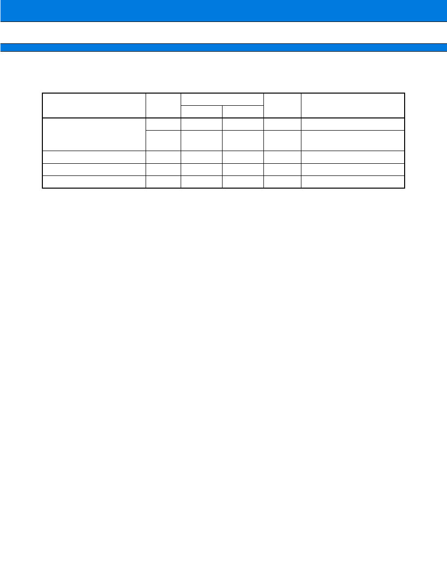
MB91106 Series
64
2.
Recommended Operating Conditions
(V
SS
= AV
SS
= 0.0 V)
Parameter
Symbol
Value
Unit
Remarks
Min.
Max.
Power supply voltage
V
CC
3.0
3.6
V
Normal operation
V
CC
3.0
3.6
V
Retaining the RAM state in
stop mode
Analog supply voltage
AV
CC
V
SS
≠ 0.3
V
SS
+ 3.6
V
Analog reference voltage
AVRH
AV
SS
AV
CC
V
Operating temperature
T
A
0
+70
∞
C
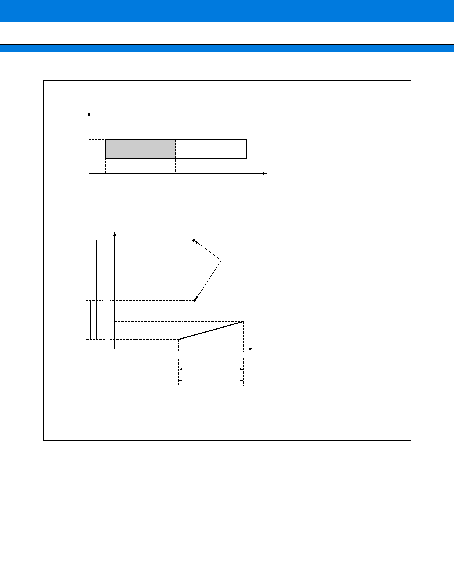
65
MB91106 Series
WARNING: The recommended operating conditions are required in order to ensure the normal operation of the
semiconductor device. All of the device's electrical characteristics are warranted when the device is
operated within these ranges.
Always use semiconductor devices within their recommended operating condition ranges. Operation
outside these ranges may adversely affect reliability and could result in device failure.
No warranty is made with respect to uses, operating conditions, or combinations not represented on
the data sheet. Users considering application outside the listed conditions are advised to contact their
FUJITSU representatives beforehand.
V
CC
(V)
Fc
(MHz)
f
CP
/f
CPP
(MHz)
f
CP
/f
CPP
(MHz)
f
CP
f
CPP
50
25
12.5
5
25
0
10
0
3.6
3.0
0
0.625
25
50
External clock
Self-oscillation
PLL system (12.5MHz(Fixed) 4 multiplication)
Divide-by-2 system
Normal operation warranty range (T
A
= 0
∞
C to +70
∞
C)
Net masked area are f
CPP
.
Supply v
o
ltage
Max. inter
n
al cloc
k frequency setting
Notes:
∑
When using PLL, the external clock must be used need 12.5 MHz.
∑
PLL oscillation stabilizing period > 100
µ
s
∑
The setting of internal clock must be within above ranges.
Peripheral
Internal clock
CPU
∑ Normal operation warranty rage
∑ External/Internal clock setting rage
12.5
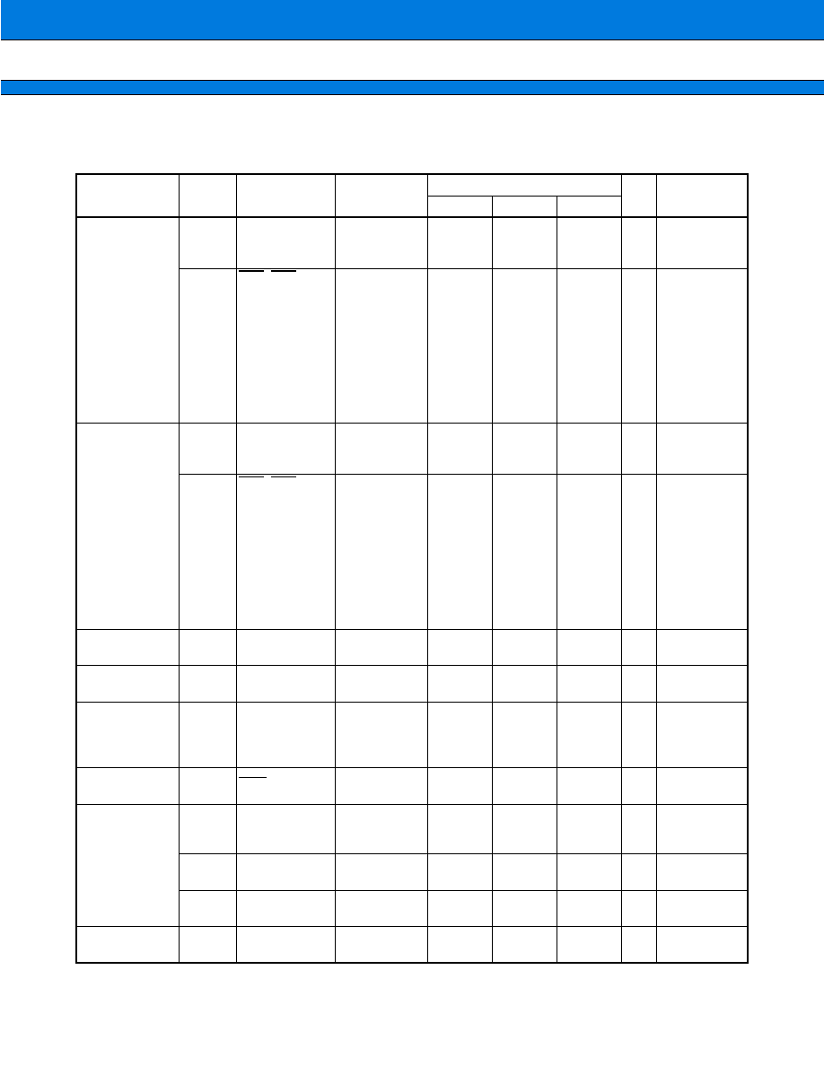
MB91106 Series
66
3.
DC Characteristics
(V
CC
= 3.0 V to 3.6 V,
V
SS
= AV
SS
= 0.0 V, T
A
= 0
∞
C to +70
∞
C)
Parameter
Symbol
Pin name
Condition
Value
Unit
Remarks
Min.
Typ.
Max.
"H" level input
voltage
V
IH
Input pin except
for hysteresis
input
--
0.7
◊
V
CC
--
V
CC
+ 0.3
V
V
IHS
NMI, RST,
P40 to P47,
P50 to P57,
P60 to P67,
P70, P81,
P83 to P85,
PA0 to PA6,
PB0 to PB7,
PE0 to PE7,
PF0 to PF7
--
0.8
◊
V
CC
--
V
CC
+ 0.3
V
Hysteresis
input
"L" level input
voltage
V
IL
Input other than
following
symbols
--
V
SS
≠ 0.3
--
0.25
◊
V
CC
V
V
ILS
NMI, RST,
P40 to P47,
P50 to P57,
P60 to P67,
P70, P81,
P83 to P85,
PA0 to PA6,
PB0 to PB7,
PE0 to PE7,
PF0 to PF7
--
V
SS
≠ 0.3
--
0.2
◊
V
CC
V
Hysteresis
input
"H" level output
voltage
V
OH
P2 to PF
V
CC
= 3.0 V
I
OH
= ≠4.0 mA
V
CC
≠ 0.5
--
--
V
"L" level output
voltage
V
OL
P8 to PF
V
CC
= 3.0 V
I
OL
= 8.0 mA
--
--
0.4
V
Input leakage
current
(Hi-Z output
leakage current)
I
LI
P2 to PF
V
CC
= 3.6 V
0.45 V < V
I
< V
CC
≠5
--
+5
µ
A
Pull-up
resistance
R
PULL
RST
V
CC
= 3.6 V
V
I
= 0.45 V
25
50
100
k
Power supply
current
I
CC
V
CC
F
C
= 12.5 MHz
V
CC
= 3.3 V
--
70
150
mA
(4 multiplication)
Operation at
50 MHz
I
CCS
V
CC
F
C
= 12.5 MHz
V
CC
= 3.3 V
--
37
70
mA Sleep mode
I
CCH
V
CC
T
A
= +25
∞
C
V
CC
= 3.3 V
--
1.4
150
µ
A Stop mode
Input
capacitance
C
IN
Except for V
CC
,
AV
CC
, AV
SS
, V
SS
--
--
10
--
pF
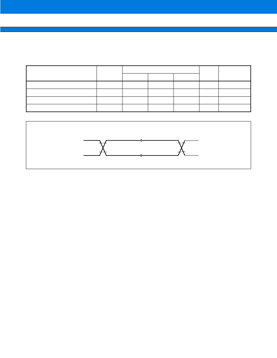
67
MB91106 Series
4.
AC Characteristics
(1) Measurement Conditions
(V
CC
= 3.0 V to 3.6 V)
* : Input rise/fall time is 10 ns. and less.
Parameter
Symbol
Value
Unit
Remarks
Min.
Typ.
Max.
"H" level input voltage
V
IH
--
1/2*
◊
V
CC
--
V
"L" level input voltage
V
IL
--
1/2*
◊
V
CC
--
V
"H" level output voltage
V
OH
--
1/2*
◊
V
CC
--
V
"L" level output voltage
V
OL
--
1/2*
◊
V
CC
--
V
Input
V
CC
0.0 V
∑Output
V
IH
V
IL
V
OH
V
OL
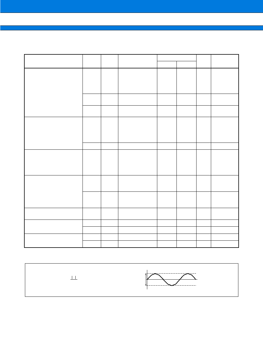
MB91106 Series
68
(2) Clock Timing Rating
(V
CC
= 3.0 V to 3.6 V,
V
SS
= AV
SS
= 0.0 V, T
A
= 0
∞
C to +70
∞
C)
*1: Frequency shift ratio stands for deviation ratio of the operating clock from the center frequency in the clock
multiplication system.
*2: These values are for a minimum clock of 10 MHz input to X0, a divide-by-2 system of the source oscillation and
a 1/8 gear.
Parameter
Symbol
Pin
name
Condition
Value
Unit
Remarks
Min.
Max.
Clock frequency
F
C
X0, X1
Self-oscillation at
12.5 MHz
Internal operation
at 50 MHz (Via
PLL,quadruplex)
12.5
12.5
MHz
F
C
X0, X1
Self-oscillation
(divide-by-2 input)
10
25
MHz
F
C
X0, X1
External clock
(divide-by-2 input)
10
25
MHz
Clock cycle time
t
C
X0, X1
Self-oscillation at
12.5 MHz
Internal operation
at 50 MHz (Via
PLL,quadruplex)
--
80
ns
t
C
X0, X1
--
40
100
ns
Frequency shift ratio
(when locked)
f
--
Self-oscillation at
12.5 MHz
Internal operation
at 50 MHz (Via
PLL,quadruplex)
--
5
%
*1
Input clock pulse width
P
WH
,
P
WL
X0, X1
12.5 MHz to
25.0 MHz
20
--
ns
Input clock
pulse to X0
and X1
P
WH
X0
12.5 MHz and less
25
--
ns
Input clock
pulse to X0
only
Input clock rising/falling time
t
CR
,
t
CF
X0, X1
--
--
8
ns
(t
CR
+ t
CF
)
Internal operating clock
frequency
f
CP
--
CPU system
0.625*
2
50
MHz
f
CPP
--
Peripheral system
0.625*
2
25
MHz
Internal operating clock
cycle time
t
CP
--
CPU system
20
1600*
2
ns
t
CPP
--
Peripheral system
40
1600*
2
ns
+
≠
f
0
≠
+
Center frequency
f =
f
0
◊
100 (%)
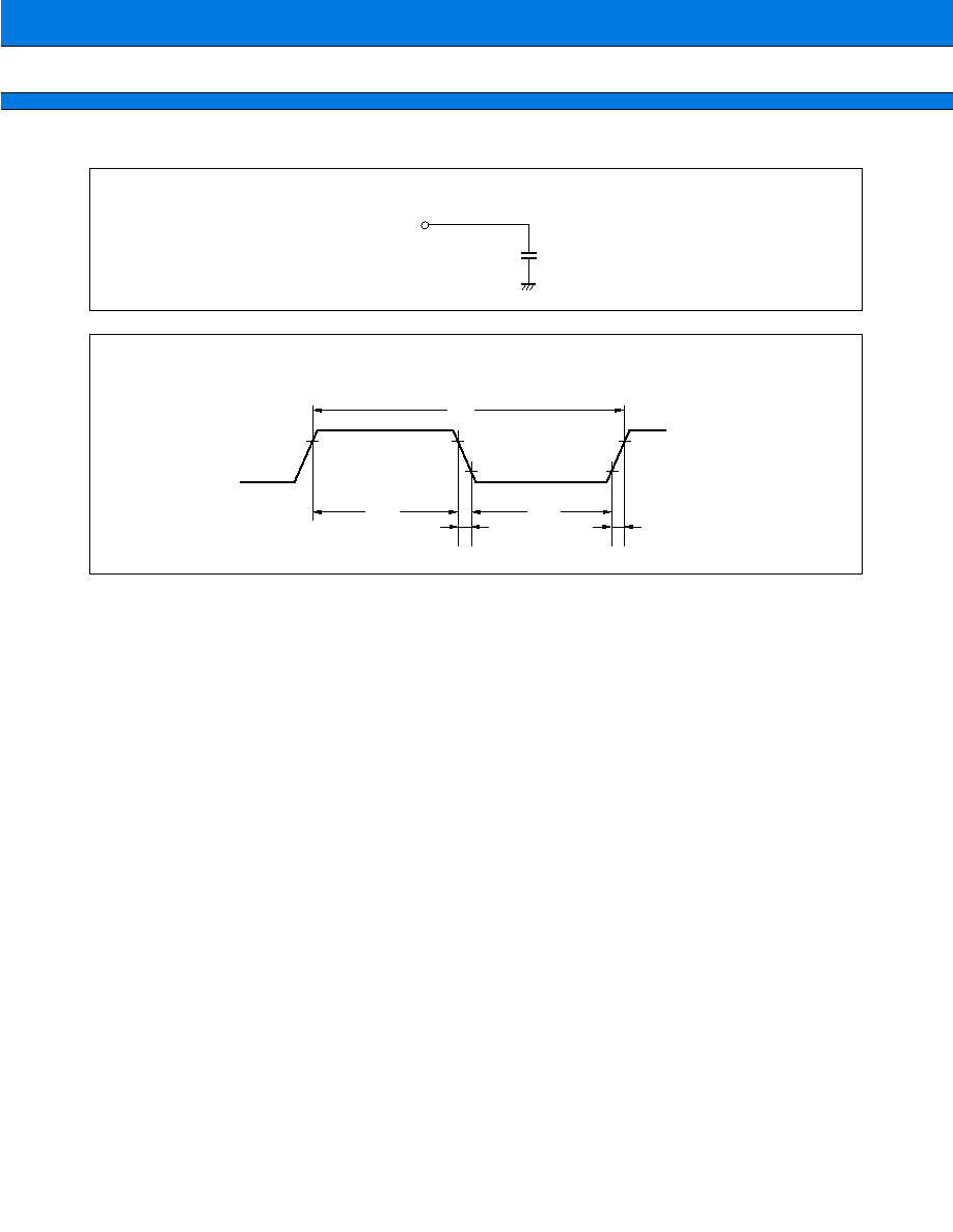
69
MB91106 Series
∑ Load conditions
∑ Clock timing rating measurement conditions
Output pin
C = 50 pF
0.8 V
CC
0.8 V
CC
0.8 V
CC
0.2 V
CC
0.2 V
CC
P
WH
t
CF
t
CR
t
C
P
WL
X0
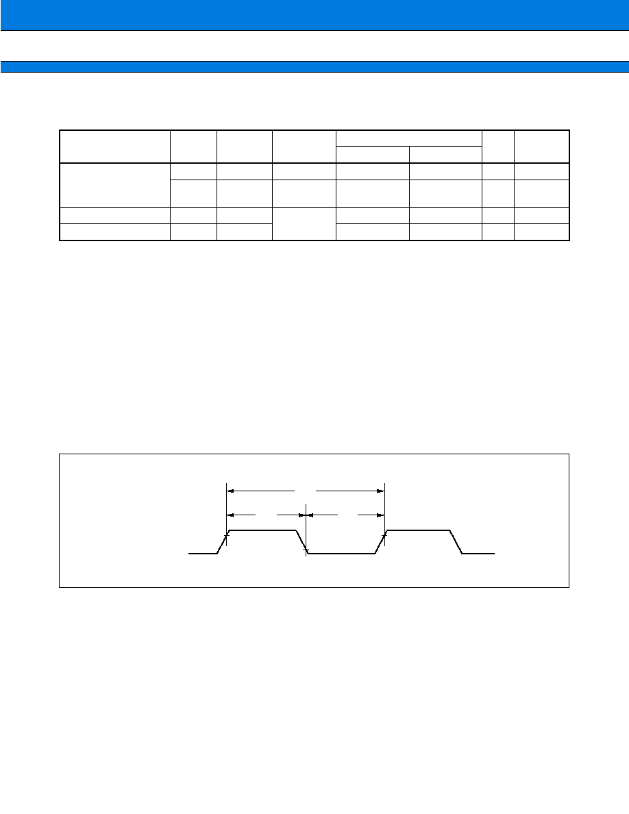
MB91106 Series
70
(3) Clock Output Timing
(V
CC
= 3.0 V to 3.6 V,
V
SS
= AV
SS
= 0.0 V, T
A
= 0
∞
C to +70
∞
C)
*1: For information on t
CP
(internal operating clock cycle time), see "(2) Clock Timing Rating."
*2: t
CYC
is a frequency for 1 clock cycle including a gear cycle.
Use the doublure when CPU frequency is above 25 MHz.
*3: Rating at a gear cycle of
◊
1.
When a gear cycle of 1/2, 1/4, 1/8 is selected, substitute "n" in the following equations with 1/2, 1/4, 1/8,
respectively.
Min. : (1 ≠ n/2)
◊
t
CYC
≠ 10
Max. : (1 ≠ n/2)
◊
t
CYC
+ 10
Select a gear cycle of
◊
1 when using the doublure.
*4: Rating at a gear cycle of
◊
1.
When a gear cycle of 1/2, 1/4, 1/8 is selected, substitute "n" in the following equations with 1/2, 1/4, 1/8,
respectively.
Min. : n/2
◊
t
CYC
≠ 10
Max. : n/2
◊
t
CYC
+ 10
Select a gear cycle of
◊
1 when using the doublure.
Parameter
Symbol
Pin name
Condition
Value
Unit
Remarks
Min.
Max.
Cycle time
t
CYC
CLK
--
t
CP
*
1
--
ns
*2
t
CYC
CLK
Using the
doublure
2
◊
t
CP
*
1
--
ns
CLK
CLK
t
CHCL
CLK
--
1/2
◊
t
CYC
≠ 5
1/2
◊
t
CYC
+ 5
ns
*3
CLK
CLK
t
CLCH
CLK
1/2
◊
t
CYC
≠ 5
1/2
◊
t
CYC
+ 5
ns
*4
CLK
t
CYC
t
CHCL
t
CLCH
V
OH
V
OH
V
OL
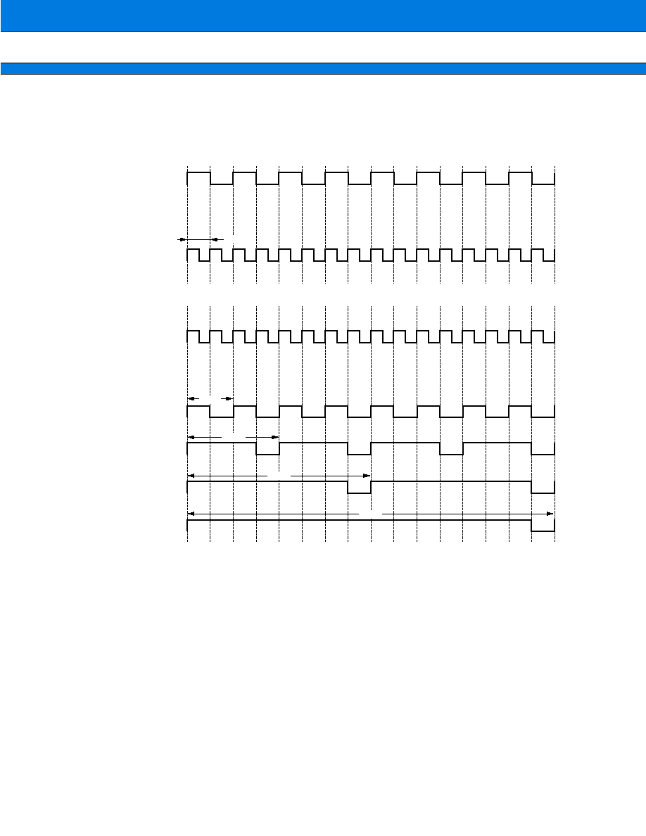
71
MB91106 Series
The relation between source oscillation input and CLK pin for configured by CHC/CCK1/CCK0 settings of GCR
(gear control register) is as follows:
However, in this chart source oscillation input means X0 input clock.
Source oscillation input
(when using the doublure)
(1) PLL system
(CHC bit of GCR set to "0")
(a) Gear
◊
1 CLK pin
CCK1/0: "00"
Source oscillation input
(2) 2 dividing system
(CHC bit of GCR set to "1")
(a) Gear
◊
1 CLK pin
CCK1/0: "00"
(b) Gear
◊
1/2 CLK pin
CCK1/0: "01"
(c) Gear
◊
1/4 CLK pin
CCK1/0: "10"
(d) Gear
◊
1/8 CLK pin
CCK1/0: "11"
t
CYC
t
CYC
t
CYC
t
CYC
t
CYC
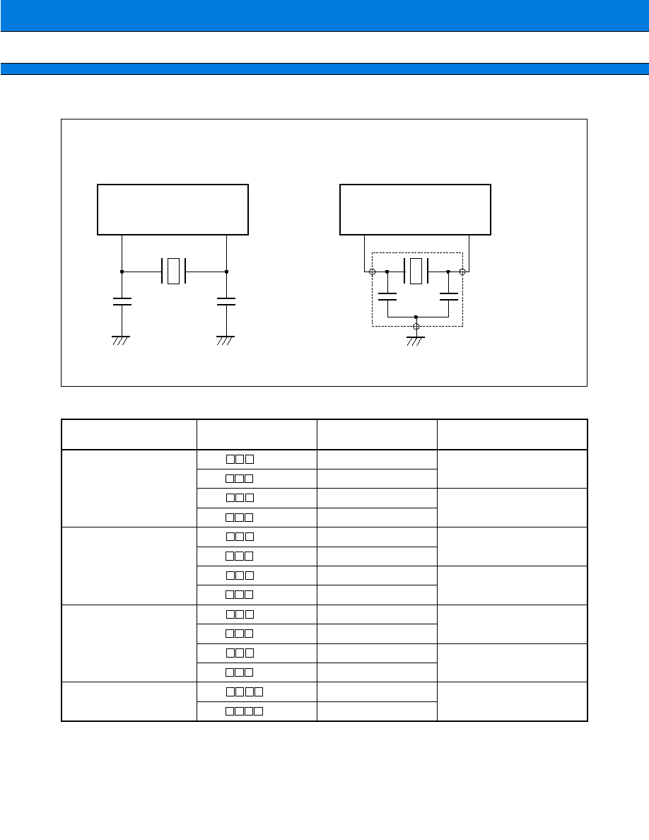
MB91106 Series
72
∑ Discreet type
( ): C
1
and C
2
internally connected 3 contacts type.
Oscillation frequency
[MHz]
Model
Load capacitance
C
1
= C
2
[pF]
Power supply voltage
V
CC
[V]
5.00 to 6.30
CSA
MG
30
2.9 to 5.5
CST
MGW
(30)
CSA
MG093
30
2.7 to 5.5
CST
MGW093
(30)
6.31 to 10.0
CSA
MTZ
30
2.9 to 5.5
CST
MTW
(30)
CSA
MTZ093
30
2.7 to 5.5
CST
MTW093
(30)
10.1 to 13.0
CSA
MTZ
30
3.0 to 5.5
CST
MTW
(30)
CSA
MTZ093
30
2.9 to 5.5
CST
MTW093
(30)
13.01 to 15.00
CSA
MXZ040
15
3.2 to 5.5
CST
MXW0C3
(15)
∑ Ceramic oscillator applications
Recommended circuit (2 contacts)
Recommended circuit (3 contacts)
*
*
C
1
C
2
C
1
C
2
X0
X1
X0
X1
* : Murata Mfg. Co., Ltd.
C
1
, C
2
internally
connected.
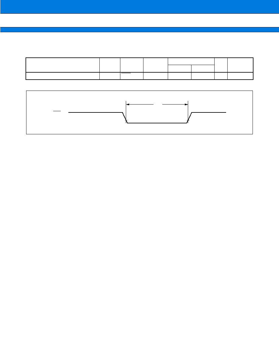
73
MB91106 Series
(4) Reset Input Ratings
(V
CC
= 3.0 V to 3.6 V,
V
SS
= AV
SS
= 0.0 V, T
A
= 0
∞
C to +70
∞
C)
* : For information on t
CP
(internal operating clock cycle time), see "(2) Clock Timing Rating."
Parameter
Symbol Pin name Condition
Value
Unit
Remarks
Min.
Max.
Reset input time
t
RSTL
RST
--
t
CP
*
◊
5
--
ns
0.2 V
CC
t
RSTL
0.2 V
CC
RST
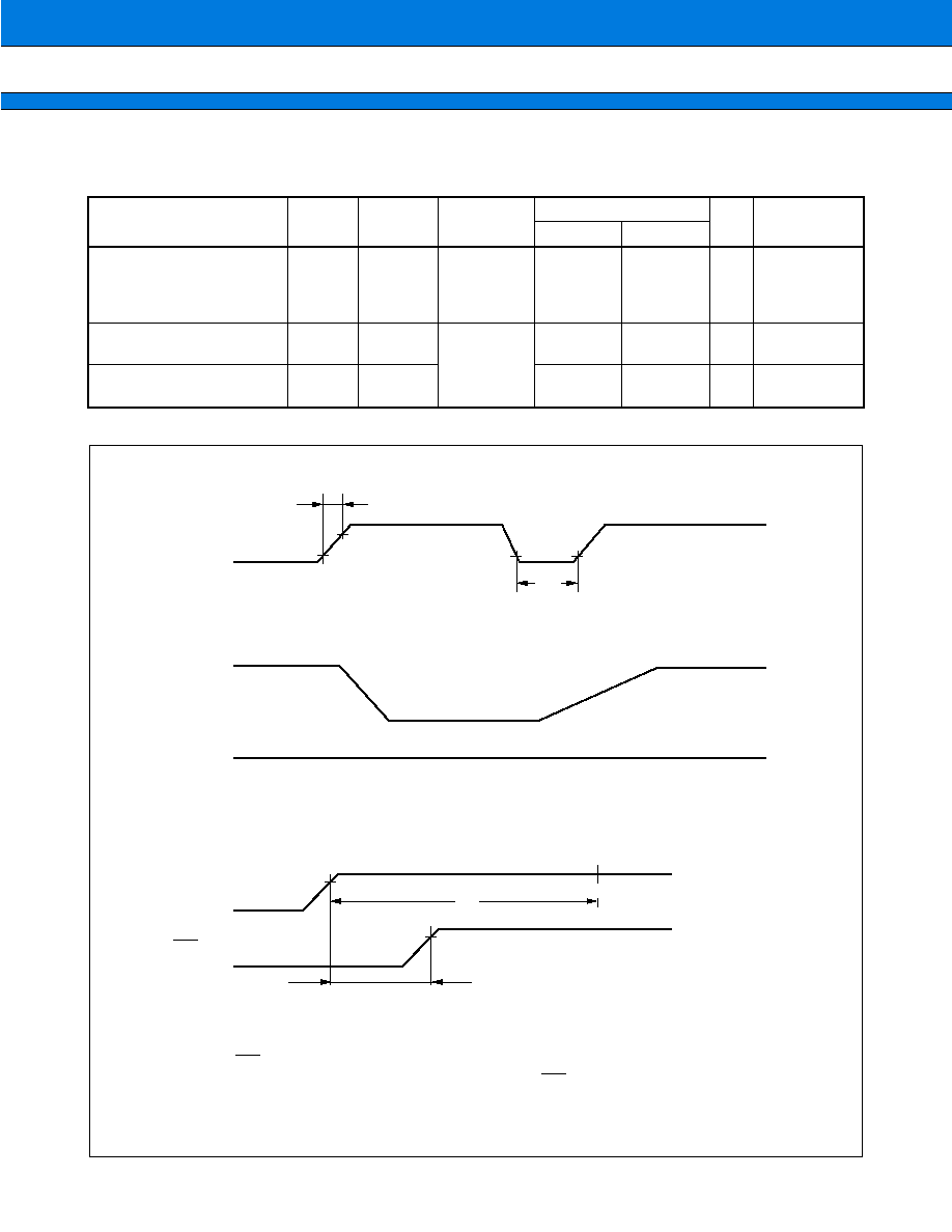
MB91106 Series
74
(5) Power on Supply Specifications (Power-on Reset)
(AV
CC
= V
CC
= 3.0 V to 3.6 V,
V
SS
= AV
SS
= 0.0 V, T
A
= 0
∞
C to +70
∞
C)
* : For information on t
C
(clock cycle time), see "(2) Clock Timing Rating."
Parameter
Symbol Pin name
Condition
Value
Unit
Remarks
Min.
Max.
Power supply rising time
t
R
V
CC
V
CC
= 3.3 V
--
18
ms
V
CC
< 0.2 V
before the
power supply
rising
Power supply shut off time
t
OFF
V
CC
--
1
--
ms
Repeated
operations
Oscillation stabilizing time
t
OSC
--
2
◊
t
C
*
◊
2
20
+ 100
µ
s
--
ns
Notes:
∑
Set RST pin to
"L" level when turning on the device, at least the described above duration after the
supply voltage reaches Vcc is necessary before turning the RST to "H" level.
∑
Some internal resistors which are initialized only via power on reset are embedded in the device.
To initialize these resistors, run power on reset by returning on the power supply.
t
OFF
t
R
t
OSC
0.8 V
CC
Note: Sudden change in supply voltage during operation may initiate a power-on sequence.
To change supply voltage during operation, it is recommended to smoothly raise the voltage to avoid rapid
fluctuations in the supply voltage.
V
CC
V
CC
V
SS
V
CC
RST
t
RSTL
: Reset input time
t
RSTL
+ (
t
C
◊
2
19
)
336 ms approx. (@12.5 MHz)
(Oscillation stabilizing time)
0.2 V
0.2 V
0.2 V
A voltage rising rate of 50 mV/ms or
less is recommended.
0.9 V
CC
75
MB91106 Series
(6) Normal Bus Access Read/write Operation
(AV
CC
= V
CC
= 3.0 V to 3.6 V,
V
SS
= AV
SS
= 0.0 V, T
A
= 0
∞
C to +70
∞
C)
*1: For information on t
CYC
(a cycle time of peripheral system clock), see "(3) Clock Output Timing."
*2: When bus timing is delayed by automatic wait insertion or RDY input, add (t
CYC
◊
extended cycle number for
delay) to this rating.
*3: Rating at a gear cycle of
◊
1.
When a gear cycle of 1/2, 1/4, 1/8 is selected, substitute "n" in the following equation with 1/2, 1/4, 1/8,
respectively.
Equation: (2 ≠ n/2)
◊
t
CYC
≠ 25
Parameter
Symbol
Pin name
Condition
Value
Unit
Remarks
Min.
Max.
CS0 to CS5 delay time
t
CHCSL
CLK,
CS0 to CS5
--
--
15
ns
t
CHCSH
CLK,
CS0 to CS5
--
15
ns
Address delay time
t
CHAV
CLK,
A24 to A00
--
15
ns
Data delay time
t
CHDV
CLK,
D31 to D16
--
15
ns
RD delay time
t
CLRL
CLK, RD
--
6
ns
t
CLRH
CLK, RD
--
6
ns
WR0, WR1 delay time
t
CLWL
CLK,
WR0, WR1
--
6
ns
t
CLWH
CLK,
WR0, WR1
--
6
ns
Valid address
valid data
input time
t
AVDV
A24 to A00,
D31 to D16
--
3/2
◊
t
CYC
*
1
≠ 25
ns
*2
*3
RD
valid data input time t
RLDV
RD,
D31 to D16
--
t
CYC
*
1
≠ 10
ns
*2
Data set up
RD
time
t
DSRH
RD,
D31 to D16
10
--
ns
RD
data hold time
t
RHDX
RD,
D31 to D16
10
--
ns
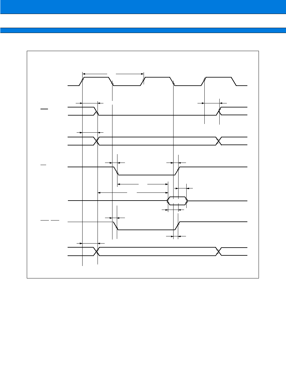
MB91106 Series
76
Write
CLK
RD
CS0 to CS5
A24 to A00
D31 to D16
WR0, WR1
D31 to D16
0.8 V
2.4 V
2.4 V
0.8 V
BA1
BA2
2.4 V
2.4 V
2.4 V
0.8 V
2.4 V
0.8 V
2.4 V
2.4 V
0.8 V
2.4 V
0.8 V
0.8 V
2.4 V
2.4 V
0.8 V
2.4 V
0.8 V
Read
t
CHCSH
t
CHCSL
0.8 V
t
CYC
t
CLRL
t
CLRH
t
RLDV
t
AVDV
t
CLWL
t
CLWH
t
CHDV
t
DSRH
t
RHDX
0.8 V
t
CHAV
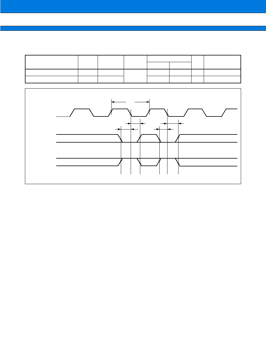
77
MB91106 Series
(7) Ready Input Timing
(V
CC
= 3.0 V to 3.6 V,
V
SS
= AV
SS
= 0.0 V, T
A
= 0
∞
C to +70
∞
C)
Parameter
Symbol
Pin name
Condition
Value
Unit
Remarks
Min.
Max.
RDY set up time
CLK
t
RDYS
RDY, CLK
--
15
--
ns
CLK
RDY hold time
t
RDYH
CLK, RDY
0
--
ns
CLK
0.8 V
2.4 V
t
RDYH
t
CYC
2.4 V
0.8 V
2.4 V
2.4 V
2.4 V
0.8 V
2.4 V
0.8 V
0.8 V
0.8 V
t
RDYS
t
RDYS
t
RDYH
RDY
When wait(s)
is inserted.
RDY
When no wait
is inserted.
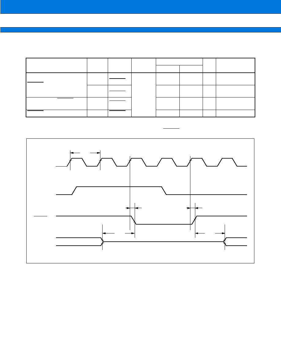
MB91106 Series
78
(8) Hold Timing
(V
CC
= 3.0 V to 3.6 V,
V
SS
= AV
SS
= 0.0 V, T
A
= 0
∞
C to +70
∞
C)
* : For information on t
CYC
(a cycle time of peripheral system clock), see "(3) Clock Output Timing."
Note: There is a delay time of more than 1 cycle from BRQ input to BGRNT change.
Parameter
Symbol Pin name Condition
Value
Unit
Remarks
Min.
Max.
BGRNT delay time
t
CHBGL
CLK,
BGRNT
--
--
6
ns
t
CHBGH
CLK,
BGRNT
--
6
ns
Pin floating
BGRNT
time
t
XHAL
BGRNT
t
CYC
* ≠ 10
t
CYC
* + 10
ns
BGRNT
pin valid time
t
HAHV
BGRNT
t
CYC
* ≠ 10
t
CYC
* + 10
ns
Each pin
0.8 V
2.4 V
t
CYC
t
CHBGL
BRQ
BGRNT
CLK
t
CHBGH
t
HAHV
t
XHAL
High impedance
2.4 V
2.4 V
2.4 V
2.4 V
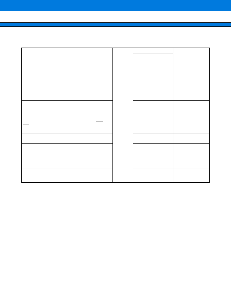
79
MB91106 Series
(9) Normal DRAM Mode Read/Write Cycle
(V
CC
= 3.0 V to 3.6 V,
V
SS
= AV
SS
= 0.0 V, T
A
= 0
∞
C to +70
∞
C)
*1: For information on t
CYC
(a cycle time of peripheral system clock), see "(3) Clock Output Timing."
*2: DW expresses that DW0, DW1 and CS0H, CS1H are used for WE.
*3: When Q1 cycle or Q4 cycle is extended for 1 cycle, add t
CYC
time to this rating.
*4: Rating at a gear cycle of
◊
1.
When a gear cycle of 1/2, 1/4, 1/8 is selected, substitute "n" in the following equation with 1/2, 1/4, 1/8,
respectively.
Equation: (3 ≠ n/2)
◊
t
CYC
≠ 16
Parameter
Symbol
Pin name
Condition
Value
Unit
Remarks
Min.
Max.
RAS delay time
t
CLRAH
CLK, RAS
--
--
6
ns
t
CHRAL
CLK, RAS
--
6
ns
CAS delay time
t
CLCASL
CLK, CS0H,
CS1H, CS0L,
CS1L
--
6
ns
t
CLCASH
CLK, CS0H,
CS1H, CS0L,
CS1L
--
6
ns
ROW address delay time
t
CHRAV
CLK,
A24 to A00
--
15
ns
COLUMN address delay
time
t
CHCAV
CLK,
A24 to A00
--
15
ns
DW delay time
t
CHDWL
CLK, DW*
2
--
15
ns
t
CHDWH
CLK, DW*
2
--
15
ns
Output data delay time
t
CHDV1
CLK,
D31 to D16
--
15
ns
RAS
valid data input
time
t
RLDV
RAS,
D31 to D16
--
5/2
◊
t
CYC
*
1
≠ 16
ns
*3
*4
CAS
valid data input
time
t
CLDV
CS0H, CS1H,
CS0L, CS1L,
D31 to D16
--
t
CYC
*
1
≠ 17
ns
*3
CAS
data hold time
t
CADH
CS0H, CS1H,
CS0L, CS1L,
D31 to D16
10
--
ns
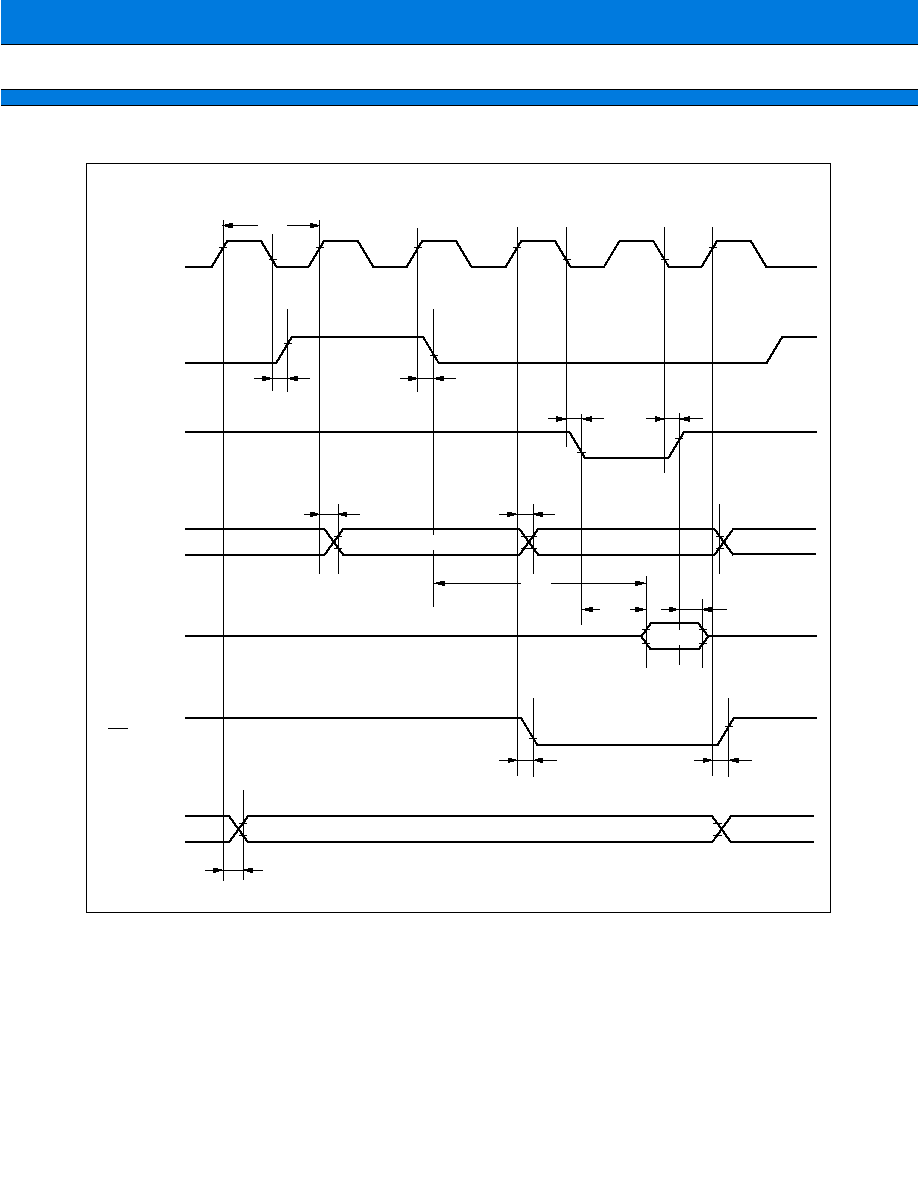
MB91106 Series
80
CLK
RAS
CS0H,
CS1H,
CS0L,
CS1L,
A24 to A00
D31 to D16
DW
D31 to D16
Q1
Q2
Q3
Q4
Q5
t
CYC
2.4 V
0.8 V
2.4 V
2.4 V
2.4 V
2.4 V
0.8 V
0.8 V
2.4 V
0.8 V
t
CLRAH
t
CHRAL
t
CLCASL
t
CLCASH
2.4 V
0.8 V
2.4 V
0.8 V
2.4 V
0.8 V
2.4 V
0.8 V
2.4 V
0.8 V
t
CHRAV
t
CHCAV
ROW address
COLUMN address
t
RLDV
t
CLDV
t
CADH
2.4 V
0.8 V
2.4 V
0.8 V
Read
2.4 V
0.8 V
2.4 V
0.8 V
t
CHDWL
t
CHDWH
t
CHDV1
2.4 V
0.8 V
Write
81
MB91106 Series
(10) Normal DRAM Mode Fast Page Read/Write Cycle
(V
CC
= 3.0 V to 3.6 V,
V
SS
= AV
SS
= 0.0 V, T
A
= 0
∞
C to +70
∞
C)
*1: For information on t
CYC
(a cycle time of peripheral system clock), see "(3) Clock Output Timing."
*2: DW expresses that DW0, DW1 and CS0H, CS1H are used for WE.
*3: When Q4 cycle is extended for 1 cycle, add t
CYC
time to this rating.
Parameter
Symbol
Pin name
Condition
Value
Unit
Remarks
Min.
Max.
RAS delay time
t
CLRAH
CLK, RAS
--
--
6
ns
CAS delay time
t
CLCASL
CLK, CS0H,
CS1H, CS0L,
CS1L
--
6
ns
t
CLCASH
CLK, CS0H,
CS1H, CS0L,
CS1L
--
6
ns
COLUMN address delay
time
t
CHCAV
CLK,
A24 to A00
--
15
ns
DW delay time
t
CHDWH
CLK, DW*
2
--
15
ns
Output data delay time
t
CHDV1
CLK,
D31 to D16
--
15
ns
CAS
valid data input
time
t
CLDV
CS0H, CS1H,
CS0L, CS1L,
D31 to D16
--
t
CYC
*
1
≠ 17
ns
*3
CAS
data hold time
t
CADH
CS0H, CS1H,
CS0L, CS1L,
D31 to D16
10
--
ns
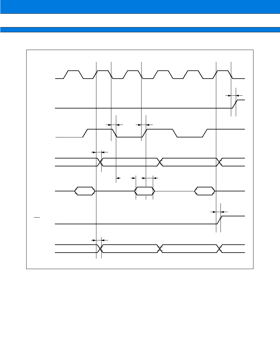
MB91106 Series
82
CLK
RAS
CS0H,
CS1H,
CS0L,
CS1L,
A24 to A00
D31 to D16
DW
D31 to D16
Q4
Q5
0.8 V
2.4 V
2.4 V
0.8 V
0.8 V
0.8 V
t
CLRAH
t
CLCASH
t
CLCASL
2.4 V
2.4 V
0.8 V
2.4 V
0.8 V
t
CHCAV
COLUMN address
t
CLDV
2.4 V
0.8 V
Read
2.4 V
2.4 V
0.8 V
t
CHDWH
t
CHDV1
Write
Q4
Q5
Q5
2.4 V
2.4 V
0.8 V
COLUMN address
COLUMN address
Read
Read
2.4 V
0.8 V
2.4 V
0.8 V
2.4 V
0.8 V
2.4 V
0.8 V
2.4 V
0.8 V
t
CADH
2.4 V
0.8 V
Write
2.4 V
0.8 V
2.4 V
0.8 V
83
MB91106 Series
(11) Single DRAM Timing
(V
CC
= 3.0 V to 3.6 V,
V
SS
= AV
SS
= 0.0 V, T
A
= 0
∞
C to +70
∞
C)
*1: For information on t
CYC
(a cycle time of peripheral system clock), see "(3) Clock Output Timing."
*2: DW expresses that DW0, DW1 and CS0H, CS1H are used for WE.
Parameter
Symbol
Pin name
Condition
Value
Unit
Remarks
Min.
Max.
RAS delay time
t
CLRAH2
CLK, RAS
--
--
6
ns
t
CHRAL2
CLK, RAS
6
ns
CAS delay time
t
CHCASL2
CLK, CS0H,
CS1H, CS0L,
CS1L
--
n/2
◊
t
CYC
*
1
ns
t
CHCASH2
CLK, CS0H,
CS1H, CS0L,
CS1L
--
6
ns
ROW address delay time
t
CHRAV2
CLK,
A24 to A00
--
15
ns
COLUMN address delay
time
t
CHCAV2
CLK,
A24 to A00
--
15
ns
DW delay time
t
CHDWL2
CLK, DW*
2
--
15
ns
t
CHDWH2
CLK, DW*
2
--
15
ns
Output data delay time
t
CHDV2
CLK,
D31 to D16
--
15
ns
CAS
Valid data input
time
t
CLDV2
CS0H, CS1H,
CS0L, CS1L,
D31 to D16
--
(1 ≠ n/2)
◊
t
CYC
*
1
≠ 17
ns
CAS
data hold time
t
CADH2
CS0H, CS1H,
CS0L, CS1L,
D31 to D16
10
--
ns
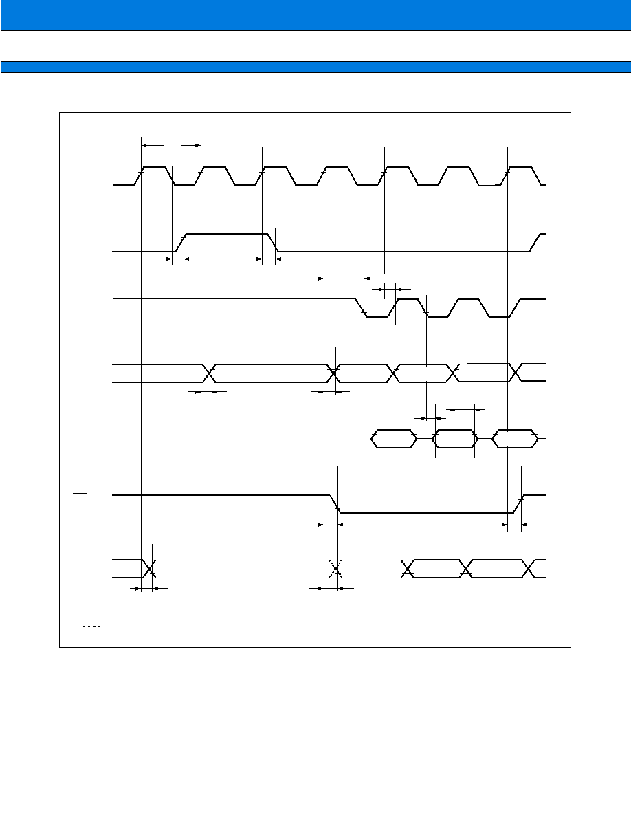
MB91106 Series
84
*1: Q4S indicates Q4SR (Read) of Single DRAM cycle or Q4SW (Write) cycle.
*2: indicates the timing when the bus cycle begins from the high spead page mode.
CLK
RAS
CS0H,
CS1H,
CS0L,
CS1L,
A24 to A00
D31 to D16
DW
D31 to D16
Q1
Q2
Q3
Q4S
t
CYC
2.4 V
0.8 V
2.4 V
2.4 V
2.4 V
2.4 V
2.4 V
0.8 V
t
CLRAH2
t
CHCASL2
2.4 V
0.8 V
2.4 V
0.8 V
2.4 V
0.8 V
2.4 V
t
CHRAV2
t
CHCAV2
ROW address
COLUMN-1
t
CLDV2
t
CADH2
2.4 V
Read-1
2.4 V
0.8 V
t
CHDWL2
t
CHDWH2
2.4 V
0.8 V
Write-0
(Read)
(Read)
(Write)
Q4S
Q4S
2.4 V
*1
t
CHRAL2
t
CHCASH2
2.4 V
0.8 V
COLUMN-2
0.8 V
COLUMN-0
Read-2
0.8 V
2.4 V
0.8 V
Read-0
*2
2.4 V
0.8 V
2.4 V
0.8 V
2.4 V
0.8 V
2.4 V
0.8 V
Write-2
t
CHDV2
t
CHDV2
Write-1
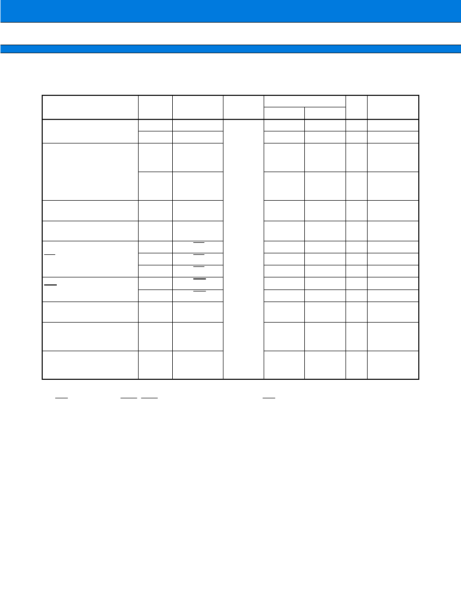
85
MB91106 Series
(12) Hyper DRAM Timing
(V
CC
= 3.0 V to 3.6 V,
V
SS
= AV
SS
= 0.0 V, T
A
= 0
∞
C to +70
∞
C)
*1: For information on t
CYC
(a cycle time of peripheral system clock), see "(3) Clock Output Timing."
*2: DW expresses that DW0, DW1 and CS0H, CS1H are used for WE.
Parameter
Symbol
Pin name
Condition
Value
Unit
Remarks
Min.
Max.
RAS delay time
t
CLRAH3
CLK, RAS
--
--
6
ns
t
CHRAL3
CLK, RAS
--
6
ns
CAS delay time
t
CHCASL3
CLK, CS0H,
CS1H, CS0L,
CS1L
--
n/2
◊
t
CYC
*
1
ns
t
CHCASH3
CLK, CS0H,
CS1H, CS0L,
CS1L
--
6
ns
ROW address delay time
t
CHRAV3
CLK,
A24 to A00
--
15
ns
COLUMN address delay
time
t
CHCAV3
CLK,
A24 to A00
--
15
ns
RD delay time
t
CHRL3
CLK, RD
--
15
ns
t
CHRH3
CLK, RD
--
15
ns
t
CLRL3
CLK, RD
--
15
ns
DW delay time
t
CHDWL3
CLK, DW*
2
--
15
ns
t
CHDWH3
CLK, DW*
2
--
15
ns
Output data delay time
t
CHDV3
CLK,
D31 to D16
--
15
ns
CAS
valid data input
time
t
CLDV3
CS0H, CS1H,
CS0L, CS1L,
D31 to D16
--
t
CYC
≠ 17
ns
CAS
data hold time
t
CADH3
CS0H, CS1H,
CS0L, CS1L,
D31 to D16
10
--
ns
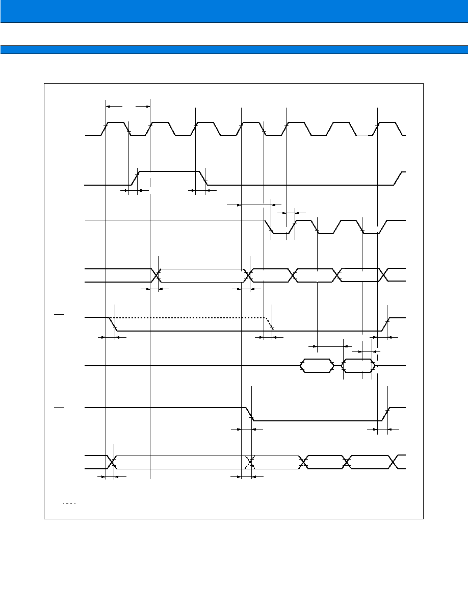
MB91106 Series
86
*1: Q4S indicates Q4SR (Read) of Single DRAM cycle or Q4SW (Write) cycle.
*2: indicates the timing when the bus cycle begins from the high spead page mode.
CLK
RAS
CS0H,
CS1H,
CS0L,
CS1L,
A24 to A00
D31 to D16
DW
D31 to D16
Q1
Q2
Q3
Q4H
t
CYC
2.4 V
0.8 V
2.4 V
2.4 V
2.4 V
2.4 V
2.4 V
0.8 V
t
CLRAH3
t
CHCASL3
2.4 V
0.8 V
2.4 V
0.8 V
2.4 V
0.8 V
2.4 V
t
CHRAV3
t
CHCAV3
ROW address
COLUMN-1
t
CLDV3
t
CADH3
2.4 V
Read-1
2.4 V
0.8 V
t
CHDWH3
2.4 V
0.8 V
(Read)
(Read)
(Write)
Q4H
Q4H
2.4 V
*1
t
CHRAL3
t
CHCASH3
2.4 V
0.8 V
COLUMN-2
0.8 V
COLUMN-0
0.8 V
2.4 V
0.8 V
Read-0
*2
2.4 V
0.8 V
2.4 V
0.8 V
Write-2
t
CHDV3
Write-1
0.8 V
0.8 V
DW
(Read)
2.4 V
0.8 V
*2
t
CLRL3
t
CHRH3
t
CHDWL3
Write-0
t
CHDV3
t
CHRL3
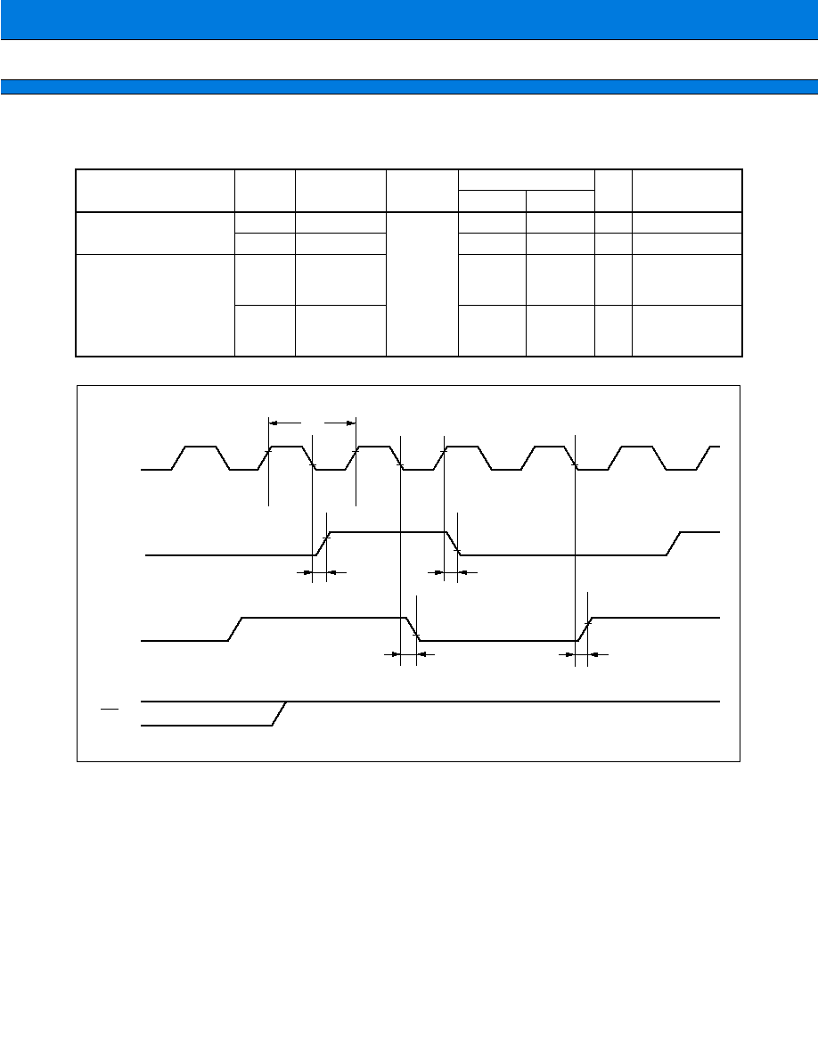
87
MB91106 Series
(13) CBR Refresh
(V
CC
= 3.0 V to 3.6 V,
V
SS
= AV
SS
= 0.0 V, T
A
= 0
∞
C to +70
∞
C)
Parameter
Symbol
Pin name
Condition
Value
Unit
Remarks
Min.
Max.
RAS delay time
t
CLRAH
CLK, RAS
--
--
6
ns
t
CHRAL
CLK, RAS
--
6
ns
CAS delay time
t
CLCASL
CLK, CS0H,
CS1H, CS0L,
CS1L
--
6
ns
t
CLCASH
CLK, CS0H,
CS1H, CS0L,
CS1L
--
6
ns
CLK
RAS
CS0H,
CS1H,
CS0L,
CS1L,
DW
R1
t
CYC
2.4 V
0.8 V
2.4 V
2.4 V
0.8 V
t
CLRAH
t
CHRAL
0.8 V
0.8 V
2.4 V
R2
R3
R4
2.4 V
0.8 V
t
CLCASL
t
CLCASH
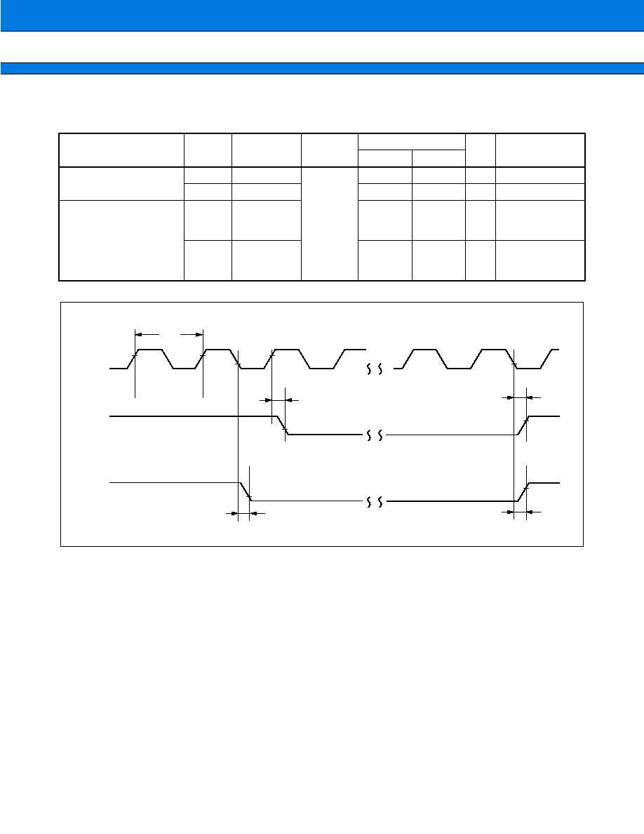
MB91106 Series
88
(14) Self Refresh
(V
CC
= 3.0 V to 3.6 V,
V
SS
= AV
SS
= 0.0 V, T
A
= 0
∞
C to +70
∞
C)
Parameter
Symbol
Pin name
Condition
Value
Unit
Remarks
Min.
Max.
RAS delay time
t
CLRAH
CLK, RAS
--
--
6
ns
t
CHRAL
CLK, RAS
--
6
ns
CAS delay time
t
CLCASL
CLK, CS0H,
CS1H, CS0L,
CS1L
--
6
ns
t
CLCASH
CLK, CS0H,
CS1H, CS0L,
CS1L
--
6
ns
CLK
RAS
CS0H,
CS1H,
CS0L,
CS1L,
SR1
t
CYC
2.4 V
0.8 V
2.4 V
2.4 V
0.8 V
2.4 V
0.8 V
t
CHRAL
t
CLRAH
t
CLCASL
t
CLCASH
2.4 V
0.8 V
SR2
SR3
SR3
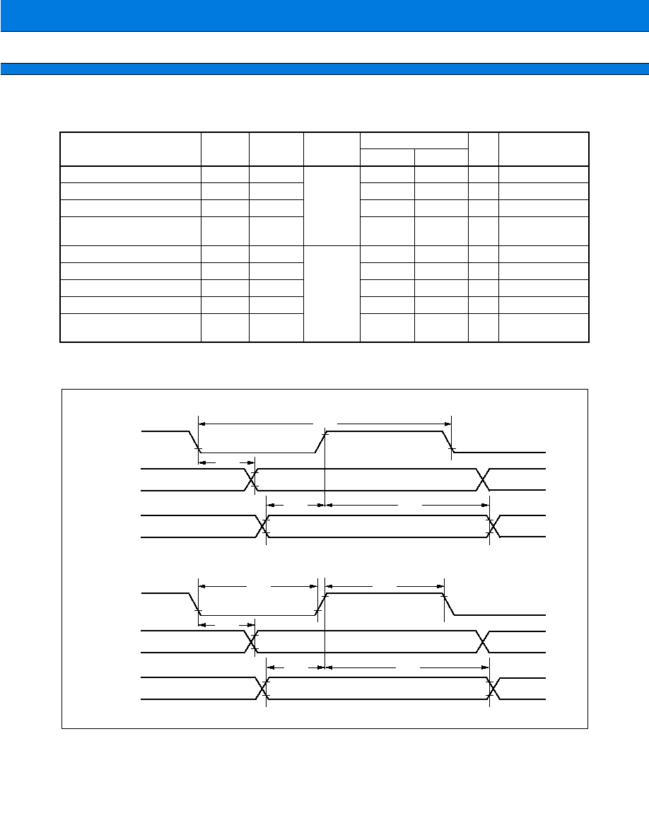
89
MB91106 Series
(15) UART Timing
(V
CC
= 3.0 V to 3.6 V,
V
SS
= AV
SS
= 0.0 V, T
A
= 0
∞
C to +70
∞
C)
* : For information on t
CYCP
(a cycle time of peripheral system clock), see "(2) Clock Timing Rating."
Notes: This rating is for AC characteristics in CLK synchronous mode.
Parameter
Symbol Pin name Condition
Value
Unit
Remarks
Min.
Max.
Serial clock cycle time
t
SCYC
--
Internal
shift clock
mode
8
◊
t
CYCP
*
--
ns
SCLK
SOUT delay time
t
SLOV
--
≠80
80
ns
Valid SIN
SCLK
t
IVSH
--
100
--
ns
SCLK
valid SIN hold
time
t
SHIX
--
60
--
ns
Serial clock "H" pulse width
t
SHSL
--
External
shift clock
mode
4
◊
t
CYCP
*
--
ns
Serial clock "L" pulse width
t
SLSH
--
4
◊
t
CYCP
*
--
ns
SCLK
SOUT delay time
t
SLOV
--
--
150
ns
Valid SIN
SCLK
t
IVSH
--
60
--
ns
SCLK
valid SIN hold
time
t
SHIX
--
60
--
ns
∑ Internal shift clock mode
∑ External shift clock mode
SCLK
SOUT
t
SCYC
0.8 V
2.4 V
0.8 V
SIN
2.4 V
0.8 V
t
SHIX
t
IVSH
0.8 V
CC
0.2 V
CC
0.8 V
CC
0.2 V
CC
SCLK
SOUT
t
SLSH
2.4 V
0.8 V
SIN
t
SHIX
t
IVSH
0.8 V
CC
0.2 V
CC
0.8 V
CC
0.2 V
CC
t
SHSL
0.8 V
CC
(2.6V)
0.2 V
CC
(0.7V)
0.2 V
CC
(0.7V)
t
SLOV
0.8 V
CC
(2.6V)
t
SLOV
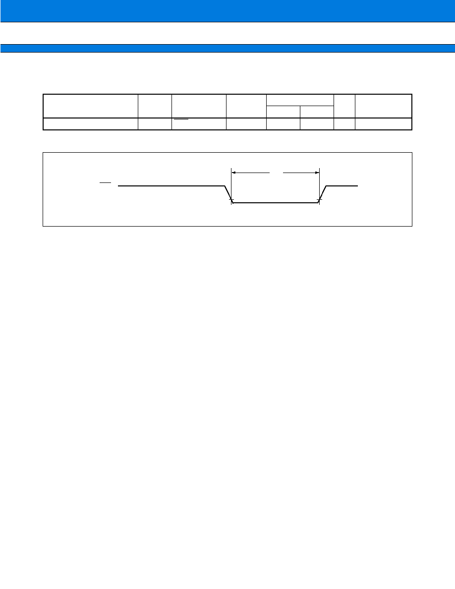
MB91106 Series
90
(16) Trigger System Input Timing
(V
CC
= 3.0 V to 3.6 V,
V
SS
= AV
SS
= 0.0 V, T
A
= 0
∞
C to +70
∞
C)
* : For information on t
CYCP
(a cycle time of peripheral system clock), see "(2) Clock Timing Rating."
Parameter
Symbol
Pin name
Condition
Value
Unit
Remarks
Min.
Max.
A/D start trigger input time
t
ATGX
ATG
--
5
◊
t
CYCP
*
--
ns
t
ATGX
0.2 V
CC
0.2 V
CC
ATG
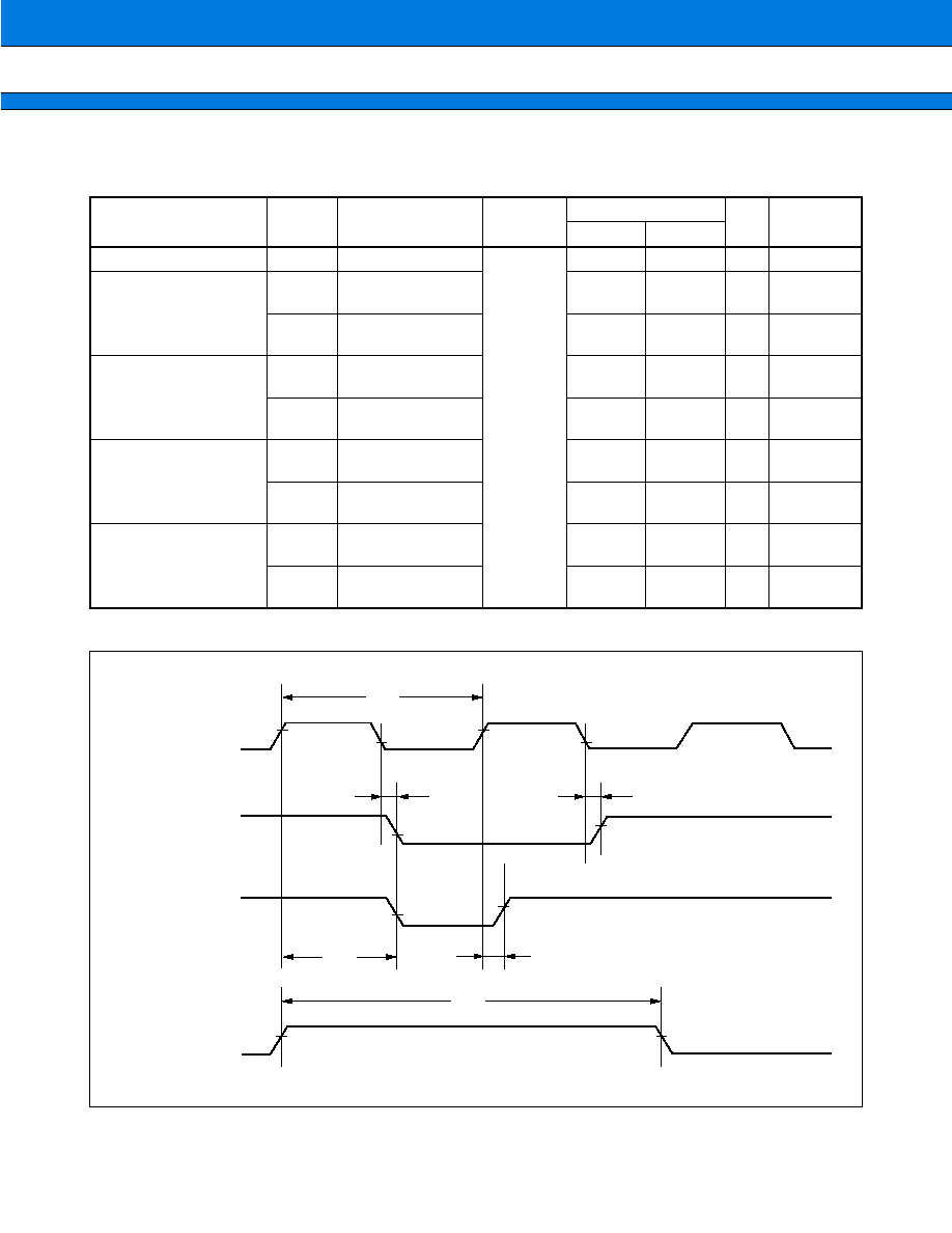
91
MB91106 Series
(17) DMA Controller Timing
(V
CC
= 3.0 V to 3.6 V,
V
SS
= AV
SS
= 0.0 V, T
A
= 0
∞
C to +70
∞
C)
* : For information on t
CYC
(a cycle time of peripheral system clock), see "(3) Clock Output Timing."
Parameter
Symbol
Pin name
Condition
Value
Unit
Remarks
Min.
Max.
DREQ input pulse width t
DRWH
DREQ0 to DREQ2
--
2
◊
t
CYC
*
--
ns
DACK delay time
(Normal bus)
(Normal DRAM)
t
CLDL
CLK,
DACK0 to DACK2
--
6
ns
t
CLDH
CLK,
DACK0 to DACK2
--
6
ns
EOP delay time
(Normal bus)
(Normal DRAM)
t
CLEL
CLK,
EOP0 to EOP2
--
6
ns
t
CLEH
CLK,
EOP0 to EOP2
--
6
ns
DACK delay time
(Single DRAM)
(Hyper DRAM)
t
CHDL
CLK,
DACK0 to DACK2
--
n/2
◊
t
CYC
*
ns
t
CHDH
CLK,
DACK0 to DACK2
--
6
ns
EOP delay time
(Single DRAM)
(Hyper DRAM)
t
CHEL
CLK,
EOP0 to EOP2
--
n/2
◊
t
CYC
*
ns
t
CHEH
CLK,
EOP0 to EOP2
--
6
ns
CLK
DACK0 to DACK2
EOP0 to EOP2
(Normal bus)
(Normal DRAM)
t
CYC
2.4 V
0.8 V
2.4 V
2.4 V
0.8 V
t
CLDL
0.8 V
0.8 V
2.4 V
t
CLEL
t
CLDH
t
CLEH
2.4 V
2.4 V
t
CHDL
t
CHEL
t
DRWH
t
CHDH
DACK0 to DACK2
EOP0 to EOP2
(Single DRAM)
(Hyper DRAM)
DREQ0 to DREQ2
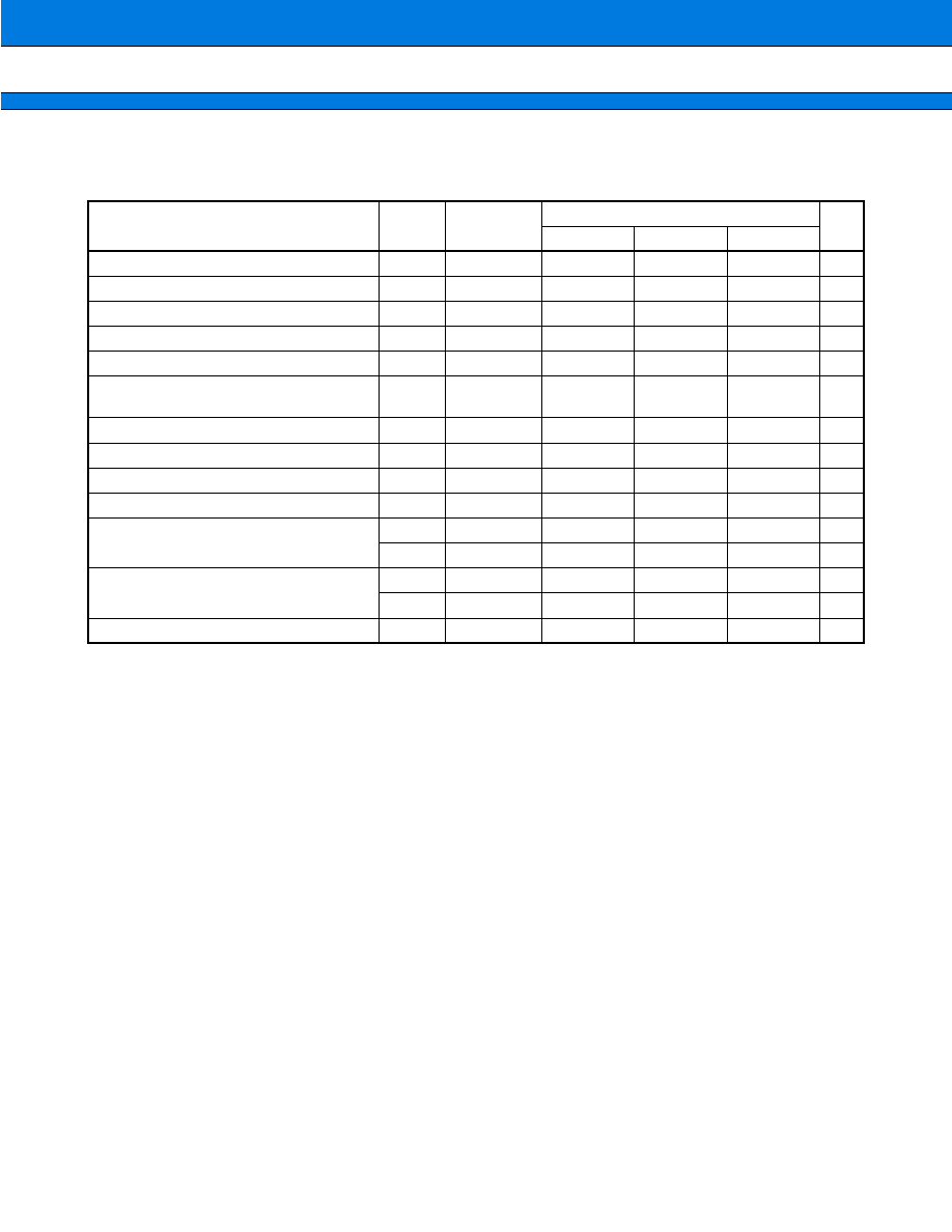
MB91106 Series
92
5.
A/D Converter Block Electrical Characteristics
(V
CC
= AV
CC
= 3.0 V to 3.6 V, V
SS
= AV
SS
= 0.0 V, AVRH = 3.0 V to 3.6 V, T
A
= 0
∞
C to +70
∞
C)
*1: V
CC
= AV
CC
= 3.0 V to 3.6 V, machine clock 25 MHz
*2: Current value for A/D converters not in operation, CPU stop mode (V
CC
= AV
CC
= AVRH = 3.6 V)
Parameter
Symbol
Pin name
Value
Unit
Min.
Typ.
Max.
Resolution
--
--
--
10
10
bit
Total error
--
--
--
--
±
3.0
LSB
Linearity error
--
--
--
--
±
2.5
LSB
Differentiation linearity error
--
--
--
--
±
1.9
LSB
Zero transition voltage
V
OT
AN0 to AN3
≠1.5LSB
+0.5LSB
+2.5LSB
mV
Full-scale transition voltage
V
FST
AN0 to AN3
AVRH ≠
4.5LSB
AVRH ≠
1.5LSB
AVRH +
0.5LSB
mV
Conversion time
--
--
5.6 *
1
--
--
µ
s
Analog port input current
I
AIN
AN0 to AN3
--
0.1
10
µ
A
Analog input voltage
V
AIN
AN0 to AN3
AV
SS
--
AVRH
V
Reference voltage
--
AVRH
AV
SS
--
AV
CC
V
Power supply current
I
A
AV
CC
--
4
--
mA
I
AH
AV
CC
--
--
5 *
2
µ
A
Reference voltage supply current
I
R
AVRH
--
110
--
µ
A
I
RH
AVRH
--
--
5 *
2
µ
A
Conversion variance between channels
--
AN0 to AN3
--
--
4
LSB
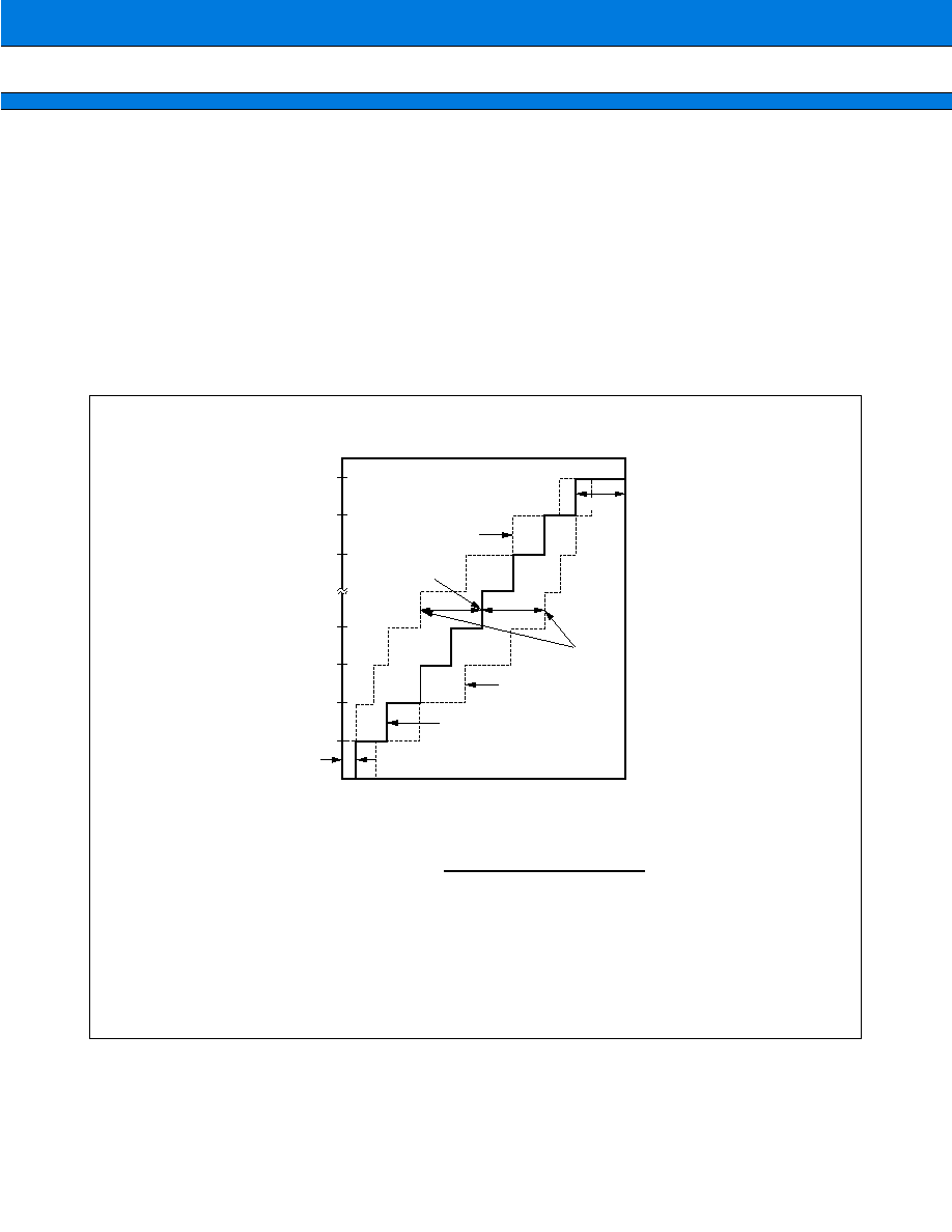
93
MB91106 Series
6.
A/D Converter Glossary
∑ Resolution
The smallest change in analog voltage detected by A/D converter.
∑ Linearity error
A deviation of actual conversion characteristic from a line connecting the zero-traction point (between "00 0000
0000"
"00 0000 0001") to the full-scale transition point (between "11 1111 1110"
"11 1111 1111").
∑ Differential linearity error
A deviation of a step voltage for changing the LSB of output code from ideal input voltage.
∑ Total error
A difference between actual value and theoretical value. The overall error includes zero-transition error, full-
scale transition error and linearity error.
(Continued)
3FF
3FE
3FD
004
003
002
001
Total error
1.5 LSB'
Actual conversion
characteristic
{1 LSB'
◊
(N ≠ 1)
+ 0.5 LSB'}
V
NT
(measured value)
Actual conversion
characteristic
Ideal characteristic
AVRL
AVRH
Analog input
0.5 LSB'
Digital output
Total error of digital output N =
V
NT
≠ {1 LSB'
◊
(N ≠ 1) + 0.5 LSB'}
1 LSB'
[LSB]
V
OT
' (ideal value) = AVRL + 0.5 LSB' [V]
V
FST
' (ideal value) = AVRL ≠ 1.5 LSB' [V]
V
NT
: A voltage for causing transition of digital output from (N ≠ 1) to N
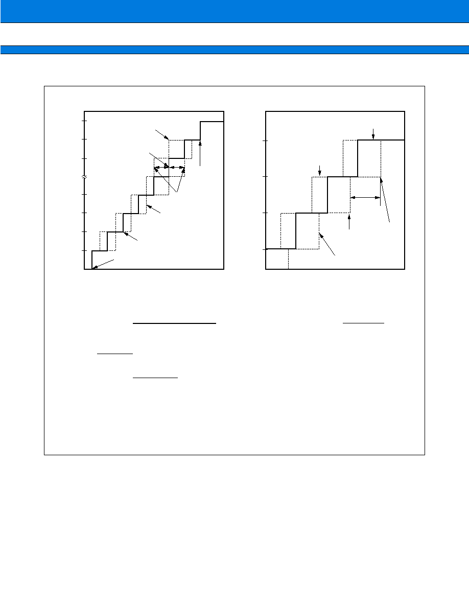
MB91106 Series
94
(Continued)
3FF
3FE
3FD
004
003
002
001
Linearity error
Actual conversion
characteristic
{1 LSB
◊
(N ≠ 1) + V
OT
}
V
NT
(measured value)
Actual conversion
characteristic
Ideal characteristic
AVRL
AVRH
Analog input
Digital output
Linearity error of
V
NT
≠ {1 LSB'
◊
(N ≠ 1) + V
OT
}
1 LSB
[LSB]
V
FST
(measured
value)
V
OT
(measured value)
N+1
Differential Iinearity error
Actual characteristic
V
NT
(measured value)
Actual conversion characteristic
AVRL
AVRH
Analog input
Digital output
N
N≠1
N≠2
Ideal characteristic
(measured value)
V
(N + 1)T
digital output N
=
Differential Iinearity error
V
(N + 1)T
≠ V
NT
1 LSB
≠1 [LSB]
of digital output N =
1 LSB' (ideal value)
AVRH ≠ AVRL
1022
[V]
=
1 LSB
V
FST
≠ V
OT
1022
[V]
=
V
OT
: A voltage for causing transition of digital output from (000)
H
to (001)
H
V
FST
: A voltage for causing transition of digital output from (3FE)
H
to (3FF)
H
V
NT
: A voltage for causing transition of digital output from (N ≠ 1)
H
to N
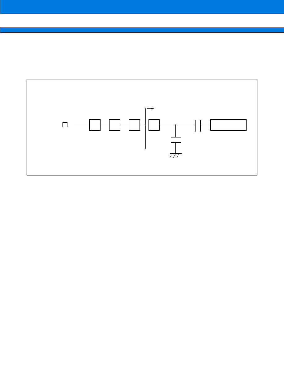
95
MB91106 Series
7.
Notes on Using A/D Converter
Output impedance of external circuit of analog input under following conditions;
Output impedance of external circuit < 7 k
.
If output impedance of external circuit is too high, analog voltage sampling time may be too short for accurate
sampling (sampling time is 5.6
µ
s for a machine clock of 25 MHz).
R
ON1
∑ Analog input Equivalent Circuit
Analog input pin
Sample hold circuit
Comparator
R
ON2
R
ON3
R
ON4
R
ON1
R
ON2
R
ON3
R
ON4
R
ON1
: 5 k
R
ON2
: 620 k
R
ON3
: 620 k
R
ON4
: 620 k
C
1
C
0
C
0
: 2 pF
C
1
: 2 pF
∑ Error
As the absolute value of AVRH decreases, relative error increases.
MB91106 Series
96
s
EXAMPLE CHARACTERISTICS
(1) "H" Level Output Voltage
(3) "H" Level Input Voltage/"L" Level
Input Voltage (CMOS Input)
(2) "L" Level Output Voltage
(4) "H" Level Input Voltage/"L" Level
Input Voltage (Hysteresis Input)
4.0
3.5
3.0
2.5
2.0
1.5
1.0
0.5
0.0
V
OH
(V)
V
OH
-I
OH
V
CC
= 3.6 V
V
CC
= 3.3 V
V
CC
= 3.0 V
V
CC
= 2.7 V
I
OH
(mA)
T
A
= +25
∞
C
-1
-2
-3
-4
-5
-6
-7
-8
0.25
0.20
0.15
0.10
0.05
0.00
V
OL
(V)
V
OL
-I
OL
V
CC
= 2.7 V
V
CC
= 3.0 V
V
CC
= 3.3 V
V
CC
= 3.6 V
I
OL
(mA)
T
A
= +25
∞
C
1
2
3
4
5
6
7
8
2.4
2.2
2.0
1.8
1.6
1.4
1.2
1.0
0.8
0.6
0.4
V
IN
(V)
V
IN
-V
CC
V
CC
(V)
T
A
= +25
∞
C
2.4
V
IH
V
IL
2.7
3.0
3.3
3.6
V
IH
: Threshold when input voltage is set to "H" Level.
V
IL
: Threshold when input voltage is set to "L" Level.
2.4
2.2
2.0
1.8
1.6
1.4
1.2
1.0
0.8
0.6
0.4
V
IN
(V)
V
IN
-V
CC
V
CC
(V)
T
A
= +25
∞
C
2.4
V
IH
V
IL
2.7
3.0
3.3
3.6
V
IH
: Threshold when input voltage in hysteresis
characteristics is set to "H" Level.
V
IL
: Threshold when input voltage in hysteresis
characteristics is set to "L" Level.
97
MB91106 Series
(5) Power Supply Current (fcp = Internal clock frequency)
(6) Pull-up Resistance
100
90
80
70
60
50
40
30
20
10
0
I
CC
(mA)
T
A
= +25
∞
C
2.7
3.0
3.3
I
CC
-V
CC
f
CP
= 50 MHz
f
CP
= 40 MHz
f
CP
= 20 MHz
f
CP
= 10 MHz
3.6
3.9
50
45
40
35
30
25
20
15
10
5
0
I
CCS
(mA)
T
A
= +25
∞
C
2.7
3.0
3.3
I
CCS
-V
CC
f
CP
= 50 MHz
f
CP
= 40 MHz
f
CP
= 20 MHz
f
CP
= 10 MHz
3.6
3.9
2.7
3.0
3.3
3.6
3.9
I
A
(mA)
T
A
= +25
∞
C
I
A
-AV
CC
2.5
2.0
1.5
1.0
0.5
0.0
2.0
1.8
1.6
1.4
1.2
1.0
0.8
0.6
0.4
0.2
0.0
I
CCH
(
µ
A)
T
A
= +25
∞
C
2.7
3.0
3.3
I
CCH
-V
CC
3.6
V
CC
(V)
V
CC
(V)
V
CC
(V)
2.7
3.0
3.3
3.6
3.9
T
A
= +25
∞
C
AV
CC
(V)
I
R
-AV
CC
I
R
(
µ
A)
130
125
120
115
110
105
100
95
90
85
80
T
A
= +25
∞
C
2.7
3.0
3.3
3.6
3.9
V
CC
(V)
AV
CC
(V)
R-V
CC
R (k
)
100
10
MB91106 Series
98
s
INSTRUCTIONS (165 INSTRUCTIONS)
1.
How to Read Instruction Set Summary
(1) Names of instructions
Instructions marked with * are not included in CPU specifications. These are extended instruction codes
added/extended at assembly language levels.
(2) Addressing modes specified as operands are listed in symbols.
Refer to "2. Addressing mode symbols" for further information.
(3) Instruction types
(4) Hexa-decimal expressions of instructions
(5) The number of machine cycles needed for execution
a: Memory access cycle and it has possibility of delay by Ready function.
b: Memory access cycle and it has possibility of delay by Ready function.
If an object register in a LD operation is referenced by an immediately following instruction, the interlock
function is activated and number of cycles needed for execution increases.
c: If an immediately following instruction operates to an object of R15, SSP or USP in read/write mode or
if the instruction belongs to instruction format A group, the interlock function is activated and number of
cycles needed for execution increases by 1 to make the total number of 2 cycles needed.
d: If an immediately following instruction refers to MDH/MDL, the interlock function is activated and number
of cycles needed for execution increases by 1 to make the total number of 2 cycles needed.
For a, b, c and d, minimum execution cycle is 1.
(6) Change in flag sign
∑ Flag change
C : Change
≠ : No change
0 : Clear
1 : Set
∑ Flag meanings
N : Negative flag
Z : Zero flag
V : Over flag
C : Carry flag
(7) Operation carried out by instruction
Mnemonic
Type
OP
CYC
NZVC
Operation
Remarks
ADD
Rj,
Ri
* ADD
#s5,
Ri
,
,
A
C
,
,
A6
A4
,
,
1
1
,
,
CCCC
CCCC
,
,
Ri + Rj
Ri
Ri + s5
Ri
,
,
(1)
(2)
(3)
(4)
(5)
(6)
(7)

99
MB91106 Series
2.
Addressing Mode Symbols
Ri
: Register direct (R0 to R15, AC, FP, SP)
Rj
: Register direct (R0 to R15, AC, FP, SP)
R13
: Register direct (R13, AC)
Ps
: Register direct (Program status register)
Rs
: Register direct (TBR, RP, SSP, USP, MDH, MDL)
CRi
: Register direct (CR0 to CR15)
CRj
: Register direct (CR0 to CR15)
#i8
: Unsigned 8-bit immediate (≠128 to 255)
Note: ≠128 to ≠1 are interpreted as 128 to 255
#i20
: Unsigned 20-bit immediate (≠0X80000 to 0XFFFFF)
Note: ≠0X7FFFF to ≠1 are interpreted as 0X7FFFF to 0XFFFFF
#i32
: Unsigned 32-bit immediate (≠0X80000000 to 0XFFFFFFFF)
Note: ≠0X80000000 to ≠1 are interpreted as 0X80000000 to 0XFFFFFFFF
#s5
: Signed 5-bit immediate (≠16 to 15)
#s10
: Signed 10-bit immediate (≠512 to 508, multiple of 4 only)
#u4
: Unsigned 4-bit immediate (0 to 15)
#u5
: Unsigned 5-bit immediate (0 to 31)
#u8
: Unsigned 8-bit immediate (0 to 255)
#u10
: Unsigned 10-bit immediate (0 to 1020, multiple of 4 only)
@dir8
: Unsigned 8-bit direct address (0 to 0XFF)
@dir9
: Unsigned 9-bit direct address (0 to 0X1FE, multiple of 2 only)
@dir10
: Unsigned 10-bit direct address (0 to 0X3FC, multiple of 4 only)
label9
: Signed 9-bit branch address (≠0X100 to 0XFC, multiple of 2 only)
label12
: Signed 12-bit branch address (≠0X800 to 0X7FC, multiple of 2 only)
label20
: Signed 20-bit branch address (≠0X80000 to 0X7FFFF)
label32
: Signed 32-bit branch address (≠0X80000000 to 0X7FFFFFFF)
@Ri
: Register indirect (R0 to R15, AC, FP, SP)
@Rj
: Register indirect (R0 to R15, AC, FP, SP)
@(R13, Rj)
: Register relative indirect (Rj: R0 to R15, AC, FP, SP)
@(R14, disp10) : Register relative indirect (disp10: ≠0X200 to 0X1FC, multiple of 4 only)
@(R14, disp9) : Register relative indirect (disp9: ≠0X100 to 0XFE, multiple of 2 only)
@(R14, disp8) : Register relative indirect (disp8: ≠0X80 to 0X7F)
@(R15, udisp6) : Register relative (udisp6: 0 to 60, multiple of 4 only)
@Ri+
: Register indirect with post-increment (R0 to R15, AC, FP, SP)
@R13+
: Register indirect with post-increment (R13, AC)
@SP+
: Stack pop
@≠SP
: Stack push
(reglist)
: Register list

MB91106 Series
100
3.
Instruction Types
ADD, ADDN, CMP, LSL, LSR and ASR instructions only
MSB
Type A
Ri
LSB
Rj
OP
Type B
Type C
Type *C'
Type D
Type E
Type F
16 bits
4
4
8
OP
i8/o8
Ri
4
8
4
Ri
u4/m4
OP
4
4
8
OP
s5/u5
Ri
7
5
4
OP
u8/rel8/dir/reglist
8
8
OP
SUB-OP
Ri
8
4
4
OP
rel11
5
11
101
MB91106 Series
4.
Detailed Description of Instructions
∑ Add/subtract operation instructions (10 instructions)
∑ Compare operation instructions (3 instructions)
∑ Logical operation instructions (12 instructions)
Mnemonic
Type
OP
Cycle N Z V C
Operation
Remarks
ADD
Rj, Ri
* ADD
#s5, Ri
ADD
#i4, Ri
ADD2
#i4, Ri
A
C'
C
C
A6
A4
A4
A5
1
1
1
1
C C C C
C C C C
C C C C
C C C C
Ri + Rj
Ri
Ri + s5
Ri
Ri + extu (i4)
Ri
Ri + extu (i4)
Ri
MSB is interpreted as
a sign in assembly
language
Zero-extension
Sign-extension
ADDC
Rj, Ri
A
A7
1
C C C C Ri + Rj + c
Ri
Add operation with
sign
ADDN
Rj, Ri
* ADDN
#s5, Ri
ADDN
#i4, Ri
ADDN2
#i4, Ri
A
C'
C
C
A2
A0
A0
A1
1
1
1
1
≠ ≠ ≠ ≠
≠ ≠ ≠ ≠
≠ ≠ ≠ ≠
≠ ≠ ≠ ≠
Ri + Rj
Ri
Ri + s5
Ri
Ri + extu (i4)
Ri
Ri + extu (i4)
Ri
MSB is interpreted as
a sign in assembly
language
Zero-extension
Sign-extension
SUB
Rj, Ri
A
AC
1
C C C C Ri ≠ Rj
Ri
SUBC
Rj, Ri
A
AD
1
C C C C Ri ≠ Rj ≠ c
Ri
Subtract operation with
carry
SUBN
Rj, Ri
A
AE
1
≠ ≠ ≠ ≠ Ri ≠ Rj
Ri
Mnemonic
Type
OP
Cycle N Z V C
Operation
Remarks
CMP
Rj, Ri
* CMP
#s5, Ri
CMP
#i4, Ri
CMP2
#i4, Ri
A
C'
C
C
AA
A8
A8
A9
1
1
1
1
C C C C
C C C C
C C C C
C C C C
Ri ≠ Rj
Ri ≠ s5
Ri + extu (i4)
Ri + extu (i4)
MSB is interpreted as
a sign in assembly
language
Zero-extension
Sign-extension
Mnemonic
Type
OP
Cycle N Z V C
Operation
Remarks
AND
Rj, Ri
AND
Rj, @Ri
ANDH
Rj, @Ri
ANDB
Rj, @Ri
A
A
A
A
82
84
85
86
1
1 + 2a
1 + 2a
1 + 2a
C C ≠ ≠
C C ≠ ≠
C C ≠ ≠
C C ≠ ≠
Ri & = Rj
(Ri) & = Rj
(Ri) & = Rj
(Ri) & = Rj
Word
Word
Half word
Byte
OR
Rj, Ri
OR
Rj, @Ri
ORH
Rj, @Ri
ORB
Rj, @Ri
A
A
A
A
92
94
95
96
1
1 + 2a
1 + 2a
1 + 2a
C C ≠ ≠
C C ≠ ≠
C C ≠ ≠
C C ≠ ≠
Ri | = Rj
(Ri) | = Rj
(Ri) | = Rj
(Ri) | = Rj
Word
Word
Half word
Byte
EOR
Rj, Ri
EOR
Rj, @Ri
EORH
Rj, @Ri
EORB
Rj, @Ri
A
A
A
A
9A
9C
9D
9E
1
1 + 2a
1 + 2a
1 + 2a
C C ≠ ≠
C C ≠ ≠
C C ≠ ≠
C C ≠ ≠
Ri ^ = Rj
(Ri) ^ = Rj
(Ri) ^ = Rj
(Ri) ^ = Rj
Word
Word
Half word
Byte
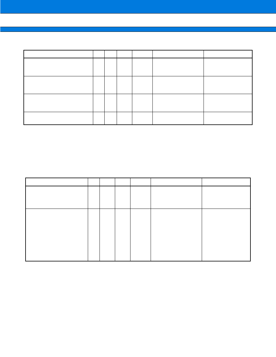
MB91106 Series
102
∑ Bit manipulation arithmetic instructions (8 instructions)
*1: Assembler generates BANDL if result of logical operation "u8&0x0F" leaves an active (set) bit and generates
BANDH if "u8&0xF0" leaves an active bit. Depending on the value in the "u8" format, both BANDL and BANDH
may be generated.
*2: Assembler generates BORL if result of logical operation "u8&0x0F" leaves an active (set) bit and generates
BORH if "u8&0xF0" leaves an active bit.
*3: Assembler generates BEORL if result of logical operation "u8&0x0F" leaves an active (set) bit and generates
BEORH if "u8&0xF0" leaves an active bit.
∑ Add/subtract operation instructions (10 instructions)
*1: DIVOS, DIV1
◊
32, DIV2, DIV3 and DIV4S are generated. A total instruction code length of 72 bytes.
*2: DIVOU and DIV1
◊
32 are generated. A total instruction code length of 66 bytes.
Mnemonic
Type
OP
Cycle N Z V C
Operation
Remarks
BANDL
#u4, @Ri(u4: 0 to 0F
H
)
BANDH
#u4, @Ri(u4: 0 to 0F
H
)
* BAND
#u8, @Ri
*
1
C
C
80
81
1 + 2a
1 + 2a
≠
≠ ≠ ≠ ≠
≠ ≠ ≠ ≠
≠ ≠ ≠ ≠
(Ri) & = (F0
H
+ u4)
(Ri) & = ((u4<<4) + 0F
H
)
(Ri) & = u8
Manipulate lower 4 bits
Manipulate upper 4
bits
BORL
#u4, @Ri(u4: 0 to 0F
H
)
BORH
#u4, @Ri(u4: 0 to 0F
H
)
* BOR
#u8, @Ri
*
2
C
C
90
91
1 + 2a
1 + 2a
≠
≠ ≠ ≠ ≠
≠ ≠ ≠ ≠
≠ ≠ ≠ ≠
(Ri) | = u4
(Ri) | = (u4<<4)
(Ri) | = u8
Manipulate lower 4 bits
Manipulate upper 4
bits
BEORL
#u4, @Ri(u4: 0 to 0F
H
)
BEORH
#u4, @Ri(u4: 0 to 0F
H
)
* BEOR
#u8, @Ri
*
3
C
C
98
99
1 + 2a
1 + 2a
≠
≠ ≠ ≠ ≠
≠ ≠ ≠ ≠
≠ ≠ ≠ ≠
(Ri) ^ = u4
(Ri) ^ = (u4<<4)
(Ri) ^ = u8
Manipulate lower 4 bits
Manipulate upper 4
bits
BTSTL
#u4, @Ri(u4: 0 to 0F
H
)
BTSTH
#u4, @Ri(u4: 0 to 0F
H
)
C
C
88
89
2 + a
2 + a
0 C ≠ ≠
C C ≠ ≠
(Ri) & u4
(Ri) & (u4<<4)
Test lower 4 bits
Test upper 4 bits
Mnemonic
Type
OP
Cycle N Z V C
Operation
Remarks
MUL
Rj, Ri
MULU
Rj, Ri
MULH
Rj, Ri
MULUH
Rj, Ri
A
A
A
A
AF
AB
BF
BB
5
5
3
3
C C C ≠
C C C ≠
C C ≠ ≠
C C ≠ ≠
Rj
◊
Ri
MDH, MDL
Rj
◊
Ri
MDH, MDL
Rj
◊
Ri
MDL
Rj
◊
Ri
MDL
32-bit
◊
32-bit = 64-bit
Unsigned
16-bit
◊
16-bit = 32-bit
Unsigned
DIVOS
Ri
DIVOU
Ri
DIV1
Ri
DIV2
Ri
DIV3
DIV4S
* DIV
Ri
*
1
* DIVU
Ri
*
2
E
E
E
E
E
E
97 ≠ 4
97 ≠ 5
97 ≠ 6
97 ≠ 7
9F ≠ 6
9F ≠ 7
1
1
d
1
1
1
≠
≠
≠ ≠ ≠ ≠
≠ ≠ ≠ ≠
≠ C ≠ C
≠ C ≠ C
≠ ≠ ≠ ≠
≠ ≠ ≠ ≠
≠ C ≠ C
≠ C ≠ C
MDL/Ri
MDL,
MDL%Ri
MDH
MDL/Ri
MDL,
MDL%Ri
MDH
Step calculation
32-bit/32-bit = 32-bit
Unsigned
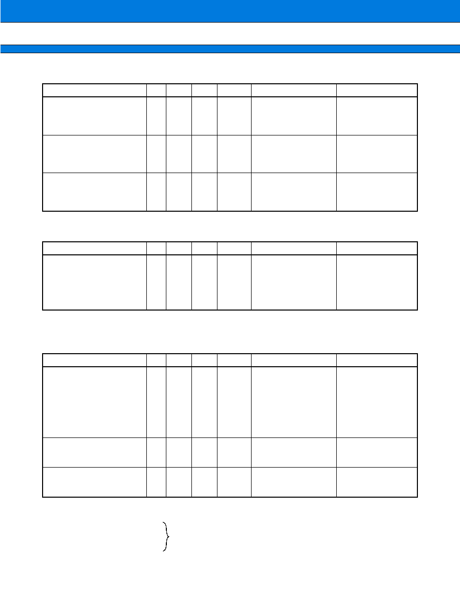
103
MB91106 Series
∑ Shift arithmetic instructions (9 instructions)
∑ Immediate value data transfer instruction (immediate value set/16-bit/32-bit immediate value transfer
instruction) (3 instructions)
*1: If an immediate value is given in absolute, assembler automatically makes i8, i20 or i32 selection.
If an immediate value contains relative value or external reference, assembler selects i32.
∑ Memory load instructions (13 instructions)
Note: The relations between o8 field of TYPE-B and u4 field of TYPE-C in the instruction format and assembler
description from disp8 to disp10 are as follows:
Mnemonic
Type
OP
Cycle N Z V C
Operation
Remarks
LSL
Rj, Ri
* LSL
#u5, Ri
LSL
#u4, Ri
LSL2
#u4, Ri
A
C'
C
C
B6
B4
B4
B5
1
1
1
1
C C ≠ C
C C ≠ C
C C ≠ C
C C ≠ C
Ri<<Rj
Ri
Ri<<u5
Ri
Ri<<u4
Ri
Ri<<(u4 + 16)
Ri
Logical shift
LSR
Rj, Ri
* LSR
#u5, Ri
LSR
#u4, Ri
LSR2
#u4, Ri
A
C'
C
C
B2
B0
B0
B1
1
1
1
1
C C ≠ C
C C ≠ C
C C ≠ C
C C ≠ C
Ri>>Rj
Ri
Ri>>u5
Ri
Ri>>u4
Ri
Ri>>(u4 + 16)
Ri
Logical shift
ASR
Rj, Ri
* ASR
#u5, Ri
ASR
#u4, Ri
ASR2
#u4, Ri
A
C'
C
C
BA
B8
B8
B9
1
1
1
1
C C ≠ C
C C ≠ C
C C ≠ C
C C ≠ C
Ri>>Rj
Ri
Ri>>u5
Ri
Ri>>u4
Ri
Ri>>(u4 + 16)
Ri
Logical shift
Mnemonic
Type
OP
Cycle N Z V C
Operation
Remarks
LDI: 32
#i32, Ri
LDI: 20
#i20, Ri
LDI: 8
#i8, Ri
* LDI
# {i8 | i20 | i32}, Ri
*
1
E
C
B
9F ≠ 8
9B
C0
3
2
1
≠
≠ ≠ ≠ ≠
≠ ≠ ≠ ≠
≠ ≠ ≠ ≠
≠ ≠ ≠ ≠
i32
Ri
i20
Ri
i8
Ri
{i8 | i20 | i32}
Ri
Upper 12 bits are zero-
extended
Upper 24 bits are zero-
extended
Mnemonic
Type
OP
Cycle N Z V C
Operation
Remarks
LD
@Rj, Ri
LD
@(R13, Rj), Ri
LD
@(R14, disp10), Ri
LD
@(R15, udisp6), Ri
LD
@R15 +, Ri
LD
@R15 +, Rs
LD
@R15 +, PS
A
A
B
C
E
E
E
04
00
20
03
07 ≠ 0
07 ≠ 8
07 ≠ 9
b
b
b
b
b
b
1 + a + b
≠ ≠ ≠ ≠
≠ ≠ ≠ ≠
≠ ≠ ≠ ≠
≠ ≠ ≠ ≠
≠ ≠ ≠ ≠
≠ ≠ ≠ ≠
C C C C
(Rj)
Ri
(R13 + Rj)
Ri
(R14 + disp10)
Ri
(R15 + udisp6)
Ri
(R15)
Ri, R15 + = 4
(R15)
Rs, R15 + = 4
(R15)
PS, R15 + = 4
Rs: Special-purpose
register
LDUH
@Rj, Ri
LDUH
@(R13, Rj), Ri
LDUH
@(R14, disp9), Ri
A
A
B
05
01
40
b
b
b
≠ ≠ ≠ ≠
≠ ≠ ≠ ≠
≠ ≠ ≠ ≠
(Rj)
Ri
(R13 + Rj)
Ri
(R14 + disp9)
Ri
Zero-extension
Zero-extension
Zero-extension
LDUB
@Rj, Ri
LDUB
@(R13, Rj), Ri
LDUB
@(R14, disp8), Ri
A
A
B
06
02
60
b
b
b
≠ ≠ ≠ ≠
≠ ≠ ≠ ≠
≠ ≠ ≠ ≠
(Rj)
Ri
(R13 + Rj)
Ri
(R14 + disp8)
Ri
Zero-extension
Zero-extension
Zero-extension
disp8
o8 = disp8
disp9
o8 = disp9>>1
disp10
o8 = disp10>>2
udisp6
u4 = udisp6>>2
Each disp is a code extension.
udisp4 is a 0 extension.
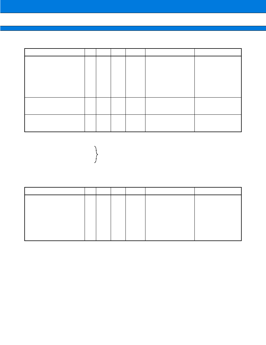
MB91106 Series
104
∑ Memory store instructions (13 instructions)
Note: The relations between o8 field of TYPE-B and u4 field of TYPE-C in the instruction format and assembler
description from disp8 to disp10 are as follows:
∑ Transfer instructions between registers/special-purpose registers transfer instructions
(5 instructions)
Mnemonic
Type
OP
Cycle N Z V C
Operation
Remarks
ST
Ri, @Rj
ST
Ri, @(R13, Rj)
ST
Ri, @(R14, disp10)
ST
Ri, @(R15, udisp6)
ST
Ri, @≠R15
ST
Rs, @≠R15
ST
PS, @≠R15
A
A
B
C
E
E
E
14
10
30
13
17 ≠ 0
17 ≠ 8
17 ≠ 9
a
a
a
a
a
a
a
≠ ≠ ≠ ≠
≠ ≠ ≠ ≠
≠ ≠ ≠ ≠
≠ ≠ ≠ ≠
≠ ≠ ≠ ≠
≠ ≠ ≠ ≠
≠ ≠ ≠ ≠
Ri
(Rj)
Ri
(R13 + Rj)
Ri
(R14 + disp10)
Ri
(R15 + usidp6)
R15 ≠ = 4, Ri
(R15)
R15 ≠ = 4, Rs
(R15)
R15 ≠ = 4, PS
(R15)
Word
Word
Word
Rs: Special-purpose
register
STH
Ri, @Rj
STH
Ri, @(R13, Rj)
STH
Ri, @(R14, disp9)
A
A
B
15
11
50
a
a
a
≠ ≠ ≠ ≠
≠ ≠ ≠ ≠
≠ ≠ ≠ ≠
Ri
(Rj)
Ri
(R13 + Rj)
Ri
(R14 + disp9)
Half word
Half word
Half word
STB
Ri, @Rj
STB
Ri, @(R13, Rj)
STB
Ri, @(R14, disp8)
A
A
B
16
12
70
a
a
a
≠ ≠ ≠ ≠
≠ ≠ ≠ ≠
≠ ≠ ≠ ≠
Ri
(Rj)
Ri
(R13 + Rj)
Ri
(R14 + disp8)
Byte
Byte
Byte
Mnemonic
Type
OP
Cycle N Z V C
Operation
Remarks
MOV
Rj, Ri
MOV
Rs, Ri
MOV
Ri, Rs
MOV
PS, Ri
MOV
Ri, PS
A
A
A
E
E
8B
B7
B3
17 ≠ 1
07 ≠ 1
1
1
1
1
c
≠ ≠ ≠ ≠
≠ ≠ ≠ ≠
≠ ≠ ≠ ≠
≠ ≠ ≠ ≠
C C C C
Rj
Ri
Rs
Ri
Ri
Rs
PS
Ri
Ri
PS
Transfer between
general-purpose
registers
Rs: Special-purpose
register
Rs: Special-purpose
register
disp8
o8 = disp8
disp9
o8 = disp9>>1
disp10
o8 = disp10>>2
udisp6
u4 = udisp6>>2
Each disp is a code extension.
udisp4 is a 0 extension.
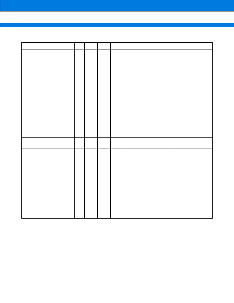
105
MB91106 Series
∑ Non-delay normal branch instructions (23 instructions)
Notes: ∑ "2/1" in cycle sections indicates that 2 cycles are needed for branch and 1 cycle needed for non-branch.
∑ The relations between rel8 field of TYPE-D and rel11 field of TYPE-F in the instruction format and
assembler discription label9 and label12 are as follows.
label9
rel8 = (label9 ≠ PC ≠ 2)/2
label12
rel11 = (label12 ≠ PC ≠ 2)/2
∑ RETI must be operated while S flag = 0.
Mnemonic
Type
OP
Cycle N Z V C
Operation
Remarks
JMP
@Ri
E
97 ≠ 0
2
≠ ≠ ≠ ≠ Ri
PC
CALL
label12
CALL
@Ri
F
E
D0
97 ≠ 1
2
2
≠ ≠ ≠ ≠
≠ ≠ ≠ ≠
PC + 2
RP,
PC + 2 + rel11
◊
2
PC
PC + 2
RP, Ri
PC
RET
E
97 ≠ 2
2
≠ ≠ ≠ ≠ RP
PC
Return
INT
#u8
D
1F
3+3a
≠ ≠ ≠ ≠ SSP ≠ = 4, PS
(SSP),
SSP ≠ = 4,
PC + 2
(SSP),
0
I flag,
0
S flag,
(TBR + 3FC ≠ u8
◊
4)
PC
INTE
E
9F ≠ 3 3 + 3a ≠ ≠ ≠ ≠ SSP ≠ = 4, PS
(SSP),
SSP ≠ = 4,
PC + 2
(SSP),
0
S flag,
(TBR + 3D8 ≠ u8
◊
4)
PC
For emulator
RETI
E
97 ≠ 3 2 + 2a C C C C (R15)
PC, R15 ≠ = 4,
(R15)
PS, R15 ≠ = 4
BNO
label9
BRA
label9
BEQ
label9
BNE
label9
BC
label9
BNC
label9
BN
label9
BP
label9
BV
label9
BNV
label9
BLT
label9
BGE
label9
BLE
label9
BGT
label9
BLS
label9
BHI
label9
D
D
D
D
D
D
D
D
D
D
D
D
D
D
D
D
E1
E0
E2
E3
E4
E5
E6
E7
E8
E9
EA
EB
EC
ED
EE
EF
1
2
2/1
2/1
2/1
2/1
2/1
2/1
2/1
2/1
2/1
2/1
2/1
2/1
2/1
2/1
≠ ≠ ≠ ≠
≠ ≠ ≠ ≠
≠ ≠ ≠ ≠
≠ ≠ ≠ ≠
≠ ≠ ≠ ≠
≠ ≠ ≠ ≠
≠ ≠ ≠ ≠
≠ ≠ ≠ ≠
≠ ≠ ≠ ≠
≠ ≠ ≠ ≠
≠ ≠ ≠ ≠
≠ ≠ ≠ ≠
≠ ≠ ≠ ≠
≠ ≠ ≠ ≠
≠ ≠ ≠ ≠
≠ ≠ ≠ ≠
Non-branch
PC + 2 + rel8
◊
2
PC
PCif Z = = 1
PCif Z = = 0
PCif C = = 1
PCif C = = 0
PCif N = = 1
PCif N = = 0
PCif V = = 1
PCif V = = 0
PCif V xor N = = 1
PCif V xor N = = 0
PCif (V xor N) or Z = = 1
PCif (V xor N) or Z = = 0
PCif C or Z = = 1
PCif C or Z = = 0
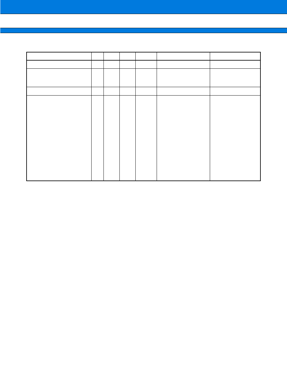
MB91106 Series
106
∑ Branch instructions with delays (20 instructions)
Notes: ∑ The relations between rel8 field of TYPE-D and rel11 field of TYPE-F in the instruction format and
assembler discription label9 and label12 are as follows.
label9
rel8 = (label9 ≠ PC ≠ 2)/2
label12
rel11 = (label12 ≠ PC ≠ 2)/2
∑ Delayed branch operation always executes next instruction (delay slot) before making a branch.
∑ Instructions allowed to be stored in the delay slot must meet one of the following conditions. If the other
instruction is stored, this device may operate other operation than defined.
The instruction described "1" in the other cycle column than branch instruction.
The instruction described "a", "b", "c" or "d" in the cycle column.
Mnemonic
Type
OP
Cycle N Z V C
Operation
Remarks
JMP:D
@Ri
E
9F ≠ 0
1
≠ ≠ ≠ ≠ Ri
PC
CALL:D
label12
CALL:D
@Ri
F
E
D8
9F ≠ 1
1
1
≠ ≠ ≠ ≠
≠ ≠ ≠ ≠
PC + 4
RP,
PC + 2 + rel11
◊
2
PC
PC + 4
RP, Ri
PC
RET:D
E
9F ≠ 2
1
≠ ≠ ≠ ≠ RP
PC
Return
BNO:D
label9
BRA:D
label9
BEQ:D
label9
BNE:D
label9
BC:D
label9
BNC:D
label9
BN:D
label9
BP:D
label9
BV:D
label9
BNV:D
label9
BLT:D
label9
BGE:D
label9
BLE:D
label9
BGT:D
label9
BLS:D
label9
BHI:D
label9
D
D
D
D
D
D
D
D
D
D
D
D
D
D
D
D
F1
F0
F2
F3
F4
F5
F6
F7
F8
F9
FA
FB
FC
FD
FE
FF
1
1
1
1
1
1
1
1
1
1
1
1
1
1
1
1
≠ ≠ ≠ ≠
≠ ≠ ≠ ≠
≠ ≠ ≠ ≠
≠ ≠ ≠ ≠
≠ ≠ ≠ ≠
≠ ≠ ≠ ≠
≠ ≠ ≠ ≠
≠ ≠ ≠ ≠
≠ ≠ ≠ ≠
≠ ≠ ≠ ≠
≠ ≠ ≠ ≠
≠ ≠ ≠ ≠
≠ ≠ ≠ ≠
≠ ≠ ≠ ≠
≠ ≠ ≠ ≠
≠ ≠ ≠ ≠
Non-branch
PC + 2 + rel8
◊
2
PC
PCif Z = = 1
PCif Z = = 0
PCif C = = 1
PCif C = = 0
PCif N = = 1
PCif N = = 0
PCif V = = 1
PCif V = = 0
PCif V xor N = = 1
PCif V xor N = = 0
PCif (V xor N) or Z = = 1
PCif (V xor N) or Z = = 0
PCif C or Z = = 1
PCif C or Z = = 0
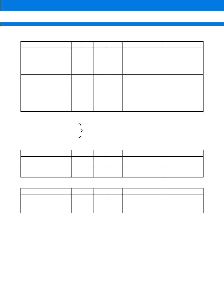
107
MB91106 Series
∑ Direct addressing instructions
Note: The relations between the dir field of TYPE-D in the instruction format and the assembler description from
disp8 to disp10 are as follows:
∑ Resource instructions (2 instructions)
∑ Co-processor instructions (4 instructions)
Mnemonic
Type
OP
Cycle N Z V C
Operation
Remarks
DMOV
@dir10, R13
DMOV
R13, @dir10
DMOV
@dir10, @R13+
DMOV
@R13+, @dir10
DMOV
@dir10, @≠R15
DMOV
@R15+, @dir10
D
D
D
D
D
D
08
18
0C
1C
0B
1B
b
a
2a
2a
2a
2a
≠ ≠ ≠ ≠
≠ ≠ ≠ ≠
≠ ≠ ≠ ≠
≠ ≠ ≠ ≠
≠ ≠ ≠ ≠
≠ ≠ ≠ ≠
(dir10)
R13
R13
(dir10)
(dir10)
(R13), R13 + = 4
(R13)
(dir10), R13 + = 4
R15 ≠ = 4, (dir10)
(R15)
(R15)
(dir10), R15 ≠ = 4
Word
Word
Word
Word
Word
Word
DMOVH
@dir9,
R13
DMOVH
R13, @dir9
DMOVH
@dir9,
@R13+
DMOVH
@R13+, @dir9
D
D
D
D
09
19
0D
1D
b
a
2a
2a
≠ ≠ ≠ ≠
≠ ≠ ≠ ≠
≠ ≠ ≠ ≠
≠ ≠ ≠ ≠
(dir9)
R13
R13
(dir9)
(dir9)
(R13), R13 + = 2
(R13)
(dir9), R13 + = 2
Half word
Half word
Half word
Half word
DMOVB
@dir8,
R13
DMOVB
R13, @dir8
DMOVB
@dir8,
@R13+
DMOVB
@R13+, @dir8
D
D
D
D
0A
1A
0E
1E
b
a
2a
2a
≠ ≠ ≠ ≠
≠ ≠ ≠ ≠
≠ ≠ ≠ ≠
≠ ≠ ≠ ≠
(dir8)
R13
R13
(dir8)
(dir8)
(R13), R13 + +
(R13)
(dir8), R13 + +
Byte
Byte
Byte
Byte
Mnemonic
Type
OP
Cycle N Z V C
Operation
Remarks
LDRES
@Ri+,
#u4
C
BC
a
≠ ≠ ≠ ≠ (Ri)
u4 resource
Ri + = 4
u4: Channel number
STRES
#u4, @Ri+
C
BD
a
≠ ≠ ≠ ≠ u4
resource
(Ri)
Ri + = 4
u4: Channel number
Mnemonic
Type
OP
Cycle N Z V C
Operation
Remarks
COPOP
#u4, #CC, CRj, CRi
COPLD
#u4, #CC, Rj,
CRi
COPST
#u4, #CC, CRj, Ri
COPSV
#u4, #CC, CRj, Ri
E
E
E
E
9F ≠ C
9F ≠ D
9F ≠ E
9F ≠ F
2 + a
1 + 2a
1 + 2a
1 + 2a
≠ ≠ ≠ ≠
≠ ≠ ≠ ≠
≠ ≠ ≠ ≠
≠ ≠ ≠ ≠
Calculation
Rj
CRi
CRj
Ri
CRj
Ri
No error traps
disp8
dir + disp8
disp9
dir = disp9>>1
disp10
dir = disp10>>2
Each disp is a code extension
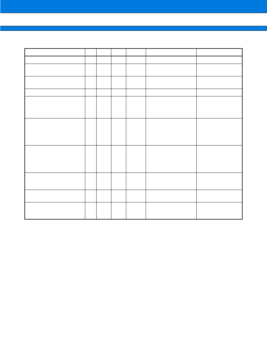
MB91106 Series
108
∑ Other instructions (16 instructions)
*1: In the ADDSP instruction, the reference between u8 of TYPE-D in the instruction format and assembler
description s10 is as follows.
s10
s8 = s10>>2
*2: In the ENTER instruction, the reference between i8 of TYPE-C in the instruction format and assembler
description u10 is as follows.
u10
u8 = u10>>2
*3: If either of R0 to R7 is specified in reglist, assembler generates LDM0. If either of R8 to R15 is specified,
assembler generates LDM1. Both LDM0 and LDM1 may be generated.
*4: The number of cycles needed for execution of LDM0 (reglist) and LDM1 (reglist) is given by the following
calculation; a
◊
(n ≠ 1) + b + 1 when "n" is number of registers specified.
*5: If either of R0 to R7 is specified in reglist, assembler generates STM0. If either of R8 to R15 is specified,
assembler generates STM1. Both STM0 and STM1 may be generated.
*6: The number of cycles needed for execution of STM0 (reglist) and STM1 (reglist) is given by the following
calculation; a
◊
n + 1 when "n" is number of registers specified.
Mnemonic
Type
OP
Cycle N Z V C
Operation
Remarks
NOP
E
9F ≠ A
1
≠ ≠ ≠ ≠ No changes
ANDCCR #u8
ORCCR
#u8
D
D
83
93
c
c
C C C C
C C C C
CCR and u8
CCR
CCR or u8
CCR
STILM
#u8
D
87
1
≠ ≠ ≠ ≠ i8
ILM
Set ILM immediate
value
ADDSP
#s10
*
1
D
A3
1
≠ ≠ ≠ ≠ R15 + = s10
ADD SP instruction
EXTSB
Ri
EXTUB
Ri
EXTSH
Ri
EXTUH
Ri
E
E
E
E
97 ≠ 8
97 ≠ 9
97 ≠ A
97 ≠ B
1
1
1
1
≠ ≠ ≠ ≠
≠ ≠ ≠ ≠
≠ ≠ ≠ ≠
≠ ≠ ≠ ≠
Sign extension 8
32 bits
Zero extension 8
32 bits
Sign extension 16
32 bits
Zero extension 16
32 bits
LDM0
(reglist)
LDM1
(reglist)
* LDM
(reglist)
*
3
D
D
8C
8D
*
4
*
4
≠
≠ ≠ ≠ ≠
≠ ≠ ≠ ≠
≠ ≠ ≠ ≠
(R15)
reglist,
R15 increment
(R15)
reglist,
R15 increment
(R15 + +)
reglist,
Load-multi R0 to R7
Load-multi R8 to R15
Load-multi R0 to R15
STM0
(reglist)
STM1
(reglist)
* STM2
(reglist)
*
5
D
D
8E
8F
*
6
*
6
≠
≠ ≠ ≠ ≠
≠ ≠ ≠ ≠
≠ ≠ ≠ ≠
R15 decrement,
reglist
(R15)
R15 decrement,
reglist
(R15)
reglist
(R15 + +)
Store-multi R0 to R7
Store-multi R8 to R15
Store-multi R0 to R15
ENTER
#u10
*
2
D
0F
1+a
≠ ≠ ≠ ≠ R14
(R15 ≠ 4),
R15 ≠ 4
R14,
R15 ≠ u10
R15
Entrance processing
of function
LEAVE
E
9F ≠ 9
b
≠ ≠ ≠ ≠ R14 + 4
R15,
(R15 ≠ 4)
R14
Exit processing of
function
XCHB
@Rj, Ri
A
8A
2a
≠ ≠ ≠ ≠ Ri
TEMP,
(Rj)
Ri,
TEMP
(Rj)
For SEMAFO
management
Byte data

109
MB91106 Series
∑ 20-bit normal branch macro instructions
*1: CALL20
(1) If label20 ≠ PC ≠ 2 is between ≠0x800 and +0x7fe, instruction is generated as follows;
CALL
label12
(2) If label20 ≠ PC ≠ 2 is outside of the range given in (1) or includes external reference symbol, instruction is
generated as follows;
LDI:20
#label20, Ri
CALL
@Ri
*2: BRA20
(1) If label20 ≠ PC ≠ 2 is between ≠0x100 and +0xfe, instruction is generated as follows;
BRA
label9
(2) If label20 ≠ PC ≠ 2 is outside of the range given in (1) or includes external reference symbol, instruction is
generated as follows;
LDI:20
#label20, Ri
JMP
@Ri
*3: Bcc20 (BEQ20 to BHI20)
(1) If label20 ≠ PC ≠ 2 is between ≠0x100 and +0xfe, instruction is generated as follows;
Bcc
label9
(2) If label20 ≠ PC ≠ 2 is outside of the range given in (1) or includes external reference symbol, instruction is
generated as follows;
Bxcc
false
xcc is a revolt condition of cc
LDI:20
#label20, Ri
JMP
@Ri
false:
Mnemonic
Operation
Remarks
* CALL20
label20, Ri
Next instruction address
RP, label20
PC
Ri: Temporary register
*
1
* BRA20
label20, Ri
* BEQ20
label20, Ri
* BNE20
label20, Ri
* BC20
label20, Ri
* BNC20
label20, Ri
* BN20
label20, Ri
* BP20
label20, Ri
* BV20
label20, Ri
* BNV20
label20, Ri
* BLT20
label20, Ri
* BGE20
label20, Ri
* BLE20
label20, Ri
* BGT20
label20, Ri
* BLS20
label20, Ri
* BHI20
label20, Ri
label20
PC
if (Z = = 1) then label20
PC
ifs/Z = = 0
ifs/C = = 1
ifs/C = = 0
ifs/N = = 1
ifs/N = = 0
ifs/V = = 1
ifs/V = = 0
ifs/V xor N = = 1
ifs/V xor N = = 0
ifs/(V xor N) or Z = = 1
ifs/(V xor N) or Z = = 0
ifs/C or Z = = 1
ifs/C or Z = = 0
Ri: Temporary register
*
2
Ri: Temporary register
*
3
Ri: Temporary register
*
3
Ri: Temporary register
*
3
Ri: Temporary register
*
3
Ri: Temporary register
*
3
Ri: Temporary register
*
3
Ri: Temporary register
*
3
Ri: Temporary register
*
3
Ri: Temporary register
*
3
Ri: Temporary register
*
3
Ri: Temporary register
*
3
Ri: Temporary register
*
3
Ri: Temporary register
*
3
Ri: Temporary register
*
3

MB91106 Series
110
∑ 20-bit delayed branch macro instructions
*1: CALL20:D
(1) If label20 ≠ PC ≠ 2 is between ≠0x800 and +0x7fe, instruction is generated as follows;
CALL:D label12
(2) If label20 ≠ PC ≠ 2 is outside of the range given in (1) or includes external reference symbol, instruction is
generated as follows;
LDI:20
#label20, Ri
CALL:D @Ri
*2: BRA20:D
(1) If label20 ≠ PC ≠ 2 is between ≠0x100 and +0xfe, instruction is generated as follows;
BRA:D
label9
(2) If label20 ≠ PC ≠ 2 is outside of the range given in (1) or includes external reference symbol, instruction is
generated as follows;
LDI:20
#label20, Ri
JMP:D
@Ri
*3: Bcc20:D (BEQ20:D to BHI20:D)
(1) If label20 ≠ PC ≠ 2 is between ≠0x100 and +0xfe, instruction is generated as follows;
Bcc:D
label9
(2) If label20 ≠ PC ≠ 2 is outside of the range given in (1) or includes external reference symbol, instruction is
generated as follows;
Bxcc
false
xcc is a revolt condition of cc
LDI:20
#label20, Ri
JMP:D
@Ri
false:
Mnemonic
Operation
Remarks
* CALL20:D label20, Ri
Next instruction address + 2
RP, label20
PC
Ri: Temporary register
*
1
* BRA20:D label20, Ri
* BEQ20:D label20, Ri
* BNE20:D label20, Ri
* BC20:D
label20, Ri
* BNC20:D label20, Ri
* BN20:D
label20, Ri
* BP20:D
label20, Ri
* BV20:D
label20, Ri
* BNV20:D label20, Ri
* BLT20:D
label20, Ri
* BGE20:D label20, Ri
* BLE20:D
label20, Ri
* BGT20:D label20, Ri
* BLS20:D
label20, Ri
* BHI20:D
label20, Ri
label20
PC
if (Z = = 1) then label20
PC
ifs/Z = = 0
ifs/C = = 1
ifs/C = = 0
ifs/N = = 1
ifs/N = = 0
ifs/V = = 1
ifs/V = = 0
ifs/V xor N = = 1
ifs/V xor N = = 0
ifs/(V xor N) or Z = = 1
ifs/(V xor N) or Z = = 0
ifs/C or Z = = 1
ifs/C or Z = = 0
Ri: Temporary register
*
2
Ri: Temporary register
*
3
Ri: Temporary register
*
3
Ri: Temporary register
*
3
Ri: Temporary register
*
3
Ri: Temporary register
*
3
Ri: Temporary register
*
3
Ri: Temporary register
*
3
Ri: Temporary register
*
3
Ri: Temporary register
*
3
Ri: Temporary register
*
3
Ri: Temporary register
*
3
Ri: Temporary register
*
3
Ri: Temporary register
*
3
Ri: Temporary register
*
3

111
MB91106 Series
∑ 32-bit normal macro branch instructions
*1: CALL32
(1) If label32 ≠ PC ≠ 2 is between ≠0x800 and +0x7fe, instruction is generated as follows;
CALL
label12
(2) If label32 ≠ PC ≠ 2 is outside of the range given in (1) or includes external reference symbol, instruction is
generated as follows;
LDI:32
#label32, Ri
CALL
@Ri
*2: BRA32
(1) If label32 ≠ PC ≠ 2 is between ≠0x100 and +0xfe, instruction is generated as follows;
BRA
label9
(2) If label32 ≠ PC ≠ 2 is outside of the range given in (1) or includes external reference symbol, instruction is
generated as follows;
LDI:32
#label32, Ri
JMP
@Ri
*3: Bcc32 (BEQ32 to BHI32)
(1) If label32 ≠ PC ≠ 2 is between ≠0x100 and +0xfe, instruction is generated as follows;
Bcc
label9
(2) If label32 ≠ PC ≠ 2 is outside of the range given in (1) or includes external reference symbol, instruction is
generated as follows;
Bxcc
false
xcc is a revolt condition of cc
LDI:32
#label32, Ri
JMP
@Ri
false:
Mnemonic
Operation
Remarks
* CALL32
label32, Ri
Next instruction address
RP, label32
PC
Ri: Temporary register
*
1
* BRA32
label32, Ri
* BEQ32
label32, Ri
* BNE32
label32, Ri
* BC32
label32, Ri
* BNC32
label32, Ri
* BN32
label32, Ri
* BP32
label32, Ri
* BV32
label32, Ri
* BNV32
label32, Ri
* BLT32
label32, Ri
* BGE32
label32, Ri
* BLE32
label32, Ri
* BGT32
label32, Ri
* BLS32
label32, Ri
* BHI32
label32, Ri
label32
PC
if (Z = = 1) then label32
PC
ifs/Z = = 0
ifs/C = = 1
ifs/C = = 0
ifs/N = = 1
ifs/N = = 0
ifs/V = = 1
ifs/V = = 0
ifs/V xor N = = 1
ifs/V xor N = = 0
ifs/(V xor N) or Z = = 1
ifs/(V xor N) or Z = = 0
ifs/C or Z = = 1
ifs/C or Z = = 0
Ri: Temporary register
*
2
Ri: Temporary register
*
3
Ri: Temporary register
*
3
Ri: Temporary register
*
3
Ri: Temporary register
*
3
Ri: Temporary register
*
3
Ri: Temporary register
*
3
Ri: Temporary register
*
3
Ri: Temporary register
*
3
Ri: Temporary register
*
3
Ri: Temporary register
*
3
Ri: Temporary register
*
3
Ri: Temporary register
*
3
Ri: Temporary register
*
3
Ri: Temporary register
*
3

MB91106 Series
112
∑ 32-bit delayed macro branch instructions
*1: CALL32:D
(1) If label32 ≠ PC ≠ 2 is between ≠0x800 and +0x7fe, instruction is generated as follows;
CALL:D label12
(2) If label32 ≠ PC ≠ 2 is outside of the range given in (1) or includes external reference symbol, instruction is
generated as follows;
LDI:32
#label32, Ri
CALL:D @Ri
*2: BRA32:D
(1) If label32 ≠ PC ≠ 2 is between ≠0x100 and +0xfe, instruction is generated as follows;
BRA:D
label9
(2) If label32 ≠ PC ≠ 2 is outside of the range given in (1) or includes external reference symbol, instruction is
generated as follows;
LDI:32
#label32, Ri
JMP:D
@Ri
*3: Bcc32:D (BEQ32:D to BHI32:D)
(1) If label32 ≠ PC ≠ 2 is between ≠0x100 and +0xfe, instruction is generated as follows;
Bcc:D
label9
(2) If label32 ≠ PC ≠ 2 is outside of the range given in (1) or includes external reference symbol, instruction is
generated as follows;
Bxcc
false
xcc is a revolt condition of cc
LDI:32
#label32, Ri
JMP:D
@Ri
false:
Mnemonic
Operation
Remarks
* CALL32:D label32, Ri
Next instruction address + 2
RP, label32
PC
Ri: Temporary register
*
1
* BRA32:D label32, Ri
* BEQ32:D label32, Ri
* BNE32:D label32, Ri
* BC32:D
label32, Ri
* BNC32:D label32, Ri
* BN32:D
label32, Ri
* BP32:D
label32, Ri
* BV32:D
label32, Ri
* BNV32:D label32, Ri
* BLT32:D
label32, Ri
* BGE32:D label32, Ri
* BLE32:D
label32, Ri
* BGT32:D label32, Ri
* BLS32:D
label32, Ri
* BHI32:D
label32, Ri
label32
PC
if (Z = = 1) then label32
PC
ifs/Z = = 0
ifs/C = = 1
ifs/C = = 0
ifs/N = = 1
ifs/N = = 0
ifs/V = = 1
ifs/V = = 0
ifs/V xor N = = 1
ifs/V xor N = = 0
ifs/(V xor N) or Z = = 1
ifs/(V xor N) or Z = = 0
ifs/C or Z = = 1
ifs/C or Z = = 0
Ri: Temporary register
*
2
Ri: Temporary register
*
3
Ri: Temporary register
*
3
Ri: Temporary register
*
3
Ri: Temporary register
*
3
Ri: Temporary register
*
3
Ri: Temporary register
*
3
Ri: Temporary register
*
3
Ri: Temporary register
*
3
Ri: Temporary register
*
3
Ri: Temporary register
*
3
Ri: Temporary register
*
3
Ri: Temporary register
*
3
Ri: Temporary register
*
3
Ri: Temporary register
*
3
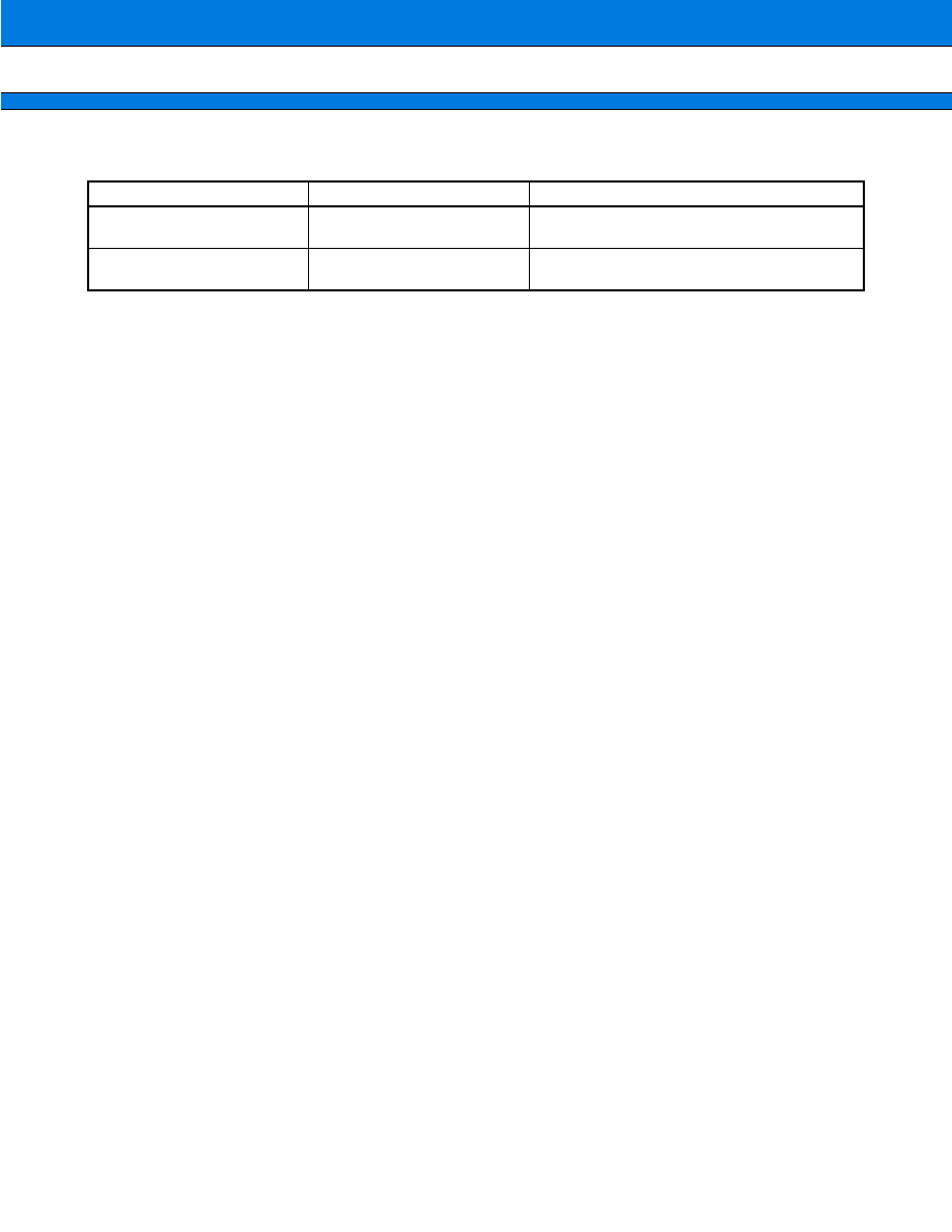
113
MB91106 Series
s
ORDERING INFORMATION
Part number
Package
Remarks
MB91106PFV-XXX
100-pin Plastic LQFP
(FPT-100P-M05)
MB91106PF-XXX
100-pin Plastic QFP
(FPT-100P-M06)
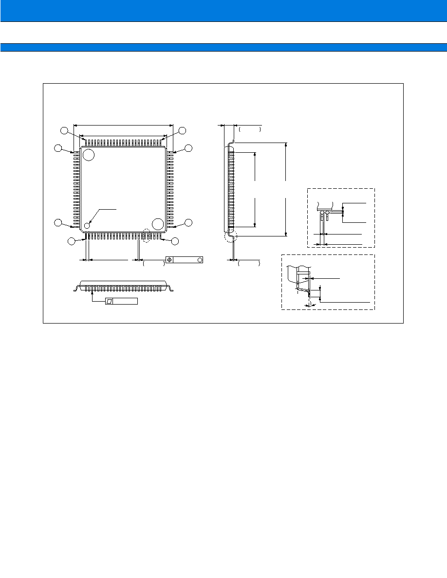
MB91106 Series
114
s
PACKAGE DIMENSIONS
Details of "B" part
16.00±0.20(.630±.008)SQ
14.00±0.10(.551±.004)SQ
0.50(.0197)TYP
.007
≠.001
+.003
≠0.03
+0.08
0.18
INDEX
0.10(.004)
0.08(.003)
M
.059
≠.004
+.008
≠0.10
+0.20
1.50
.005
≠.001
+.002
≠0.02
+0.05
0.127
15.00
12.00
(.472)
REF
(.591)
NOM
"B"
"A"
25
26
1
100
75
51
50
76
0.50±0.20(.020±.008)
Details of "A" part
0.40(.016)MAX
0.15(.006)MAX
0.15(.006)
0.15(.006)
0.10±0.10
(.004±.004)
(STAND OFF)
0~10∞
AD No.
(Mouting height)
(FPT-100P-M05)
100-pin Plastic LQFP
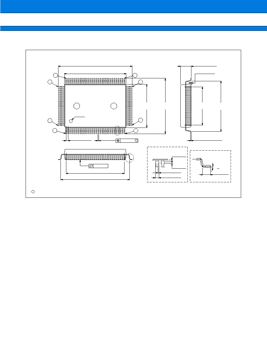
115
MB91106 Series
Note: The design may be modified changed without notice, contact to Fujitsu sales division when using the device.
C
1994 FUJITSU LIMITED F100008-3C-2
"A"
"B"
0.10(.004)
0.53(.021)MAX
0.18(.007)MAX
Details of "A" part
0 10∞
Details of "B" part
12.35(.486)
REF
16.30±0.40
(.642±.016)
0.05(.002)MIN
(STAND OFF)
0.15±0.05(.006±.002)
INDEX
23.90±0.40(.941±.016)
20.00±0.20(.787±.008)
17.90±0.40
14.00±0.20
(.551±.008)
(.705±.016)
0.13(.005)
M
18.85(.742)REF
22.30±0.40(.878±.016)
1
30
31
50
51
80
81
100
0.25(.010)
0.30(.012)
0.65(.0256)TYP
0.30±0.10
(.012±.004)
LEAD No.
0.80±0.20
(.031±.008)
3.35(.132)MAX
(Mounting height)
Dimensions in mm (inches)
(FPT-100P-M06)
100-pin Plastic QFP

MB91106 Series
116
FUJITSU LIMITED
For further information please contact:
Japan
FUJITSU LIMITED
Corporate Global Business Support Division
Electronic Devices
KAWASAKI PLANT, 4-1-1, Kamikodanaka
Nakahara-ku, Kawasaki-shi
Kanagawa 211-8588, Japan
Tel: 81(44) 754-3763
Fax: 81(44) 754-3329
http://www.fujitsu.co.jp/
North and South America
FUJITSU MICROELECTRONICS, INC.
Semiconductor Division
3545 North First Street
San Jose, CA 95134-1804, USA
Tel: (408) 922-9000
Fax: (408) 922-9179
Customer Response Center
Mon. - Fri.: 7 am - 5 pm (PST)
Tel: (800) 866-8608
Fax: (408) 922-9179
http://www.fujitsumicro.com/
Europe
FUJITSU MIKROELEKTRONIK GmbH
Am Siebenstein 6-10
D-63303 Dreieich-Buchschlag
Germany
Tel: (06103) 690-0
Fax: (06103) 690-122
http://www.fujitsu-ede.com/
Asia Pacific
FUJITSU MICROELECTRONICS ASIA PTE LTD
#05-08, 151 Lorong Chuan
New Tech Park
Singapore 556741
Tel: (65) 281-0770
Fax: (65) 281-0220
http://www.fmap.com.sg/
F9901
©
FUJITSU LIMITED Printed in Japan
All Rights Reserved.
The contents of this document are subject to change without
notice. Customers are advised to consult with FUJITSU sales
representatives before ordering.
The information and circuit diagrams in this document are
presented as examples of semiconductor device applications,
and are not intended to be incorporated in devices for actual use.
Also, FUJITSU is unable to assume responsibility for
infringement of any patent rights or other rights of third parties
arising from the use of this information or circuit diagrams.
FUJITSU semiconductor devices are intended for use in
standard applications (computers, office automation and other
office equipment, industrial, communications, and measurement
equipment, personal or household devices, etc.).
CAUTION:
Customers considering the use of our products in special
applications where failure or abnormal operation may directly
affect human lives or cause physical injury or property damage,
or where extremely high levels of reliability are demanded (such
as aerospace systems, atomic energy controls, sea floor
repeaters, vehicle operating controls, medical devices for life
support, etc.) are requested to consult with FUJITSU sales
representatives before such use. The company will not be
responsible for damages arising from such use without prior
approval.
Any semiconductor devices have an inherent chance of
failure. You must protect against injury, damage or loss from
such failures by incorporating safety design measures into your
facility and equipment such as redundancy, fire protection, and
prevention of over-current levels and other abnormal operating
conditions.
If any products described in this document represent goods or
technologies subject to certain restrictions on export under the
Foreign Exchange and Foreign Trade Law of Japan, the prior
authorization by Japanese government will be required for
export of those products from Japan.