DS07-16309-3E
FUJITSU SEMICONDUCTOR
DATA SHEET
32-Bit Microcontroller
CMOS
FR65E Series
MB91307B
s
DESCRIPTION
The FUJITSU FR family of single-chip microcontrollers using a 32-bit high-performance RISC CPU, with a variety
of built-in I/O resources and bus control mechanisms for built-in control applications requiring high-capability,
high-speed CPU processing. External bus access is assumed in order to support the expanded address space
accessible by the 32-bit CPU, and a 1 KB cache memory plus large 128 KB RAM are provided for high-speed
execution of CPU instructions.
This microcontroller is ideal for built-in applications such as DVD players, navigation systems, high-capability FAX
and printer control that demand high-capability CPU processing power.
The MB91307B is a FR65E series product based on the FR30/40 series CPU with enhanced bus access for
higher speed operation.
s
FEATURES
FR CPU
� 32-bit RISC, load/store architecture, 5-stage pipeline
� Operating frequency 66MHz [with PLL: base frequency 16.5 MHz]
� 16-bit fixed length instructions (basic instructions), 1 instruction per cycle
(Continued)
s
PACKAGE
120-pin, plastic LQFP
(FPT-120P-M21)
Purchase of Fujitsu I
2
C components conveys a license under the Philips I
2
C Patent rights to use these components
in an I
2
C system provided that the system conforms to the I
2
C Standard Specification as defined by Philips.

MB91307B
2
� Instructions for built-in applications: memory-to-memory transfer, bit processing, barrel shift etc.
� Instructions adapted for high-level languages: function input/output instructions, register contents multi-load/
store instructions
� Easier assembler notation: register interlock function
� Built-in multiplier/instruction level support
Signed 32-bit multiplication: 5 cycles
Signed 16-bit multiplication: 3 cycles
� Interrupt (PC, PS removal): 6 cycles, 16 priority levels
� Harvard architecture for simultaneous execution of program access and data access
� CPU hold 4-word queue allows advanced instruction fetch function
� 4 GB expanded memory space enables linear access
� Instruction compatible with FR30/40 family
Bus Interface
� Operating frequency: Max 33 MHz
� 8- or 16-bit data output
� Built-in pre-fetch buffer
� Unused data/address pins can be used as general-0purpose input/output ports
� Fully independent 8-area chip select outputs, can be set in minimum 64 KB units
� Interface support for many memory types
SRAM, ROM/Flash
Page mode flash ROM, page mode ROM interface
Burst mode flash ROM (select burst length 1, 2, 4, 8)
� Basic bus cycle: 2 cycles
� Programmable by area with automatic wait cycle generation to enable wait insert
� RDY input for external wait cycles
� DMA supports fly-by transfer with independent I/O wait control
Built-in RAM
� 128 KB built-in RAM capacity
� Accepts writing of data and instruction codes, enabling use as instruction RAM
Instruction cache
� 1 KB capacity
� 2-way set associative
� 4-words (16 bytes) per set
� Lock function enables permanent program storage
� Areas not used for instruction cache can be used for RAM
DMAC (DMA controller)
� 5-channel (3-channel external-to-external)
� 3 transfer sources (external pin, internal peripheral, software)
� Addressing mode with 32-bit full address indication (increment, decrement, fixed)
� Transfer mode (demand transfer / burst transfer / step transfer / block transfer)
� Fly-by transfer support (3 channels between external I/O and external memory)
� Transfer data size selection 8/16/32-bit
Bit search module (using REALOS)
� Searches words from MSB for first bit position of a 1/0 change
Reload timer (includes 1 channel for REALOS)
� 16-bit timer: 3 channels
� Internal clock multiplier choice of x2, x8, x32
(Continued)

MB91307B
3
(Continued)
UART
� Full duplex double buffer
� 3-channel
� Parity/no parity selection
� Asynchronous (start-stop synchronized), CLK-synchronized communications selection
� Built-in exclusive baud rate timer
� External clock can be used as transfer clock
� Variety of error detection functions (parity, frame, overrun)
I
2
C interface
Interrupt controller
� Total of 9 external interrupts: 1 non-maskable interrupt pin (NMI) and 8 normal interrupt pins INT7-INT0
� Interrupt from internal peripheral devices
� Programmable priority settings (16 levels) enabled, except for non-maskable interrupt
� Can be used for wake-up from stop mode
A/D converter
� 10-bit resolution, 4-channel
� Sequential comparator type, conversion time approx. 5.4
�
s
� Conversion modes: single conversion mode, continuous conversion mode
� Startup source: software / external trigger / timer output signal
Other interval timers
� 16-bit timer with 3 channels (U-timer)
� Watchdog timer
I/O port
� Maximum 69 ports
Other features
� Built-in oscillator circuit for clock source, PLL multiplier selection enabled
� INIT reset pin
� Also included: watchdog timer reset, software reset
� Power-saving modes: stop mode, sleep mode supported
� Gear functions
� Built-in time base timer
� Packages: LQFP-120 (FPT-120P-M21) : MB91307B
: MB91V307R(Evaluation product)
� CMOS technology
: 0.25
�
m
� Supply voltage
: 3.3 V
�
0.3 V (built-in regulator 3.3 V
2.5 V)
� Master/slave sending and receiving
� Arbitration function
� Clock synchronization function
� Slave address/general call address detection function
� Transfer direction detection function
� Start condition repeat generator and detection function
� Bus error detection function
� 10-bit/7-bit slave address
� Operates in standard mode (Max 100 Kbps) or high speed mode (Max 400 Kbps)
MB91307B
4
s
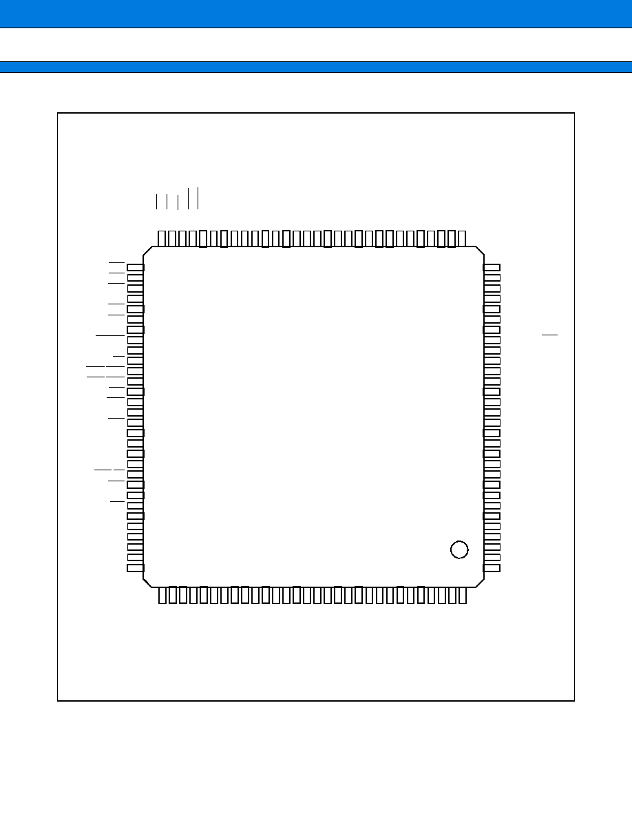
PIN ASSIGNMENT
(TOP VIEW)
(FPT-120P-M21)
* : "L" level output after initialization and reset
61
62
63
64
65
66
67
68
69
70
71
72
73
74
75
76
77
78
79
80
81
82
83
84
85
86
87
88
89
90
PA3/CS3
PA4/CS4
PA5/CS5
C
PA6/CS6
PA7/CS7
P80/RDY
P81/BGRNT
P82/BRQ
RD
UUB/WR0
P85/ULB/WR1
NMI
HST
V
SS
INIT
P90/SYSCLK
P91
P92/MCLK
P93
P94/LBA/AS
P95/BAA
P96
P97/WE
P20/D16
P21/D17
P22/D18
P23/D19
P24/D20
P25/D21
PI5/SC1
PI4/SO1
PI3/SI1
PI2/SC0
PI1/SO0
PI0/SI0
V
CC
PJ7/INT7/ATG
PJ6/INT6/TIN2
PJ5/INT5/TIN1
PJ4/INT4/TIN0
PJ3/INT3
PJ2/INT2
PJ1/INT1
PJ0/INT0
AN3
AN2
AN1
AN0
AV
SS
/AVRL
AVRH
AV
CC
A24/P70
A23/P67
A22/P66
A21/P65
A20/P64
A19/P63
A18/P62
A17/P61
30
29
28
27
26
25
24
23
22
21
20
19
18
17
16
15
14
13
12
11
10
9
8
7
6
5
4
3
2
1
91
92
93
94
95
96
97
98
99
100
101
102
103
104
105
106
107
108
109
110
111
112
113
114
115
116
117
118
119
120
P26/D22
P27/D23
D24
D25
D26
D27
D28
D29
D30
D31
V
SS
A00
A01
A02
A03
A04
A05
A06
A07
V
CC
A08
A09
A10
A11
A12
A13
A14
A15
V
SS
P60/A16
P
A2/CS2
P
A1/CS1
P
A0/CS0
PB7/IORD
PB6/IO
WR
V
CC
X0
X1
V
SS
PB5/DEOP1/DSTP1
PB4/D
A
CK1
PB3/DREQ1
PB2/DEOP0/DSTP0
PB1/D
A
CK0
PB0/DREQ0
MD2
MD1
MD0
PG2/DEOP2/DSTP2
PG1/D
A
CK2
PG0/DREQ2
PH7/SCL
PH6/SD
A
PH5/T
O
T
2
PH4/T
O
T
1
PH3/T
O
T
0
V
SS
PH2/SC2
PH1/SO2
PH0/SI2
60
59
58
57
56
55
54
53
52
51
50
49
48
47
46
45
44
43
42
41
40
39
38
37
36
35
34
33
32
31
MB91307B
5
s
PIN DESCRIPTIONS
(Continued)
Pin no.
Pin name
I/O
circuit type
Description
85 to 92
D16 to D23
C
External data bus bits 16-23
Valid only in external bus 16-bit mode.
P20 to P27
These pins can be used as ports in external bus 8-bit mode
93 to 100
D24 to D31
C
External data bus bits 24-31
102 to 109
A00 to A07
F
External address output bits 0-7
111 to 118
A08 to A15
F
External address output bits 8-15
120, 1 to 7
A16 to A23
F
External address output bits 16-23
P60 to P67
These pins can be used as ports according to setting
8
A24
F
External data bus output bit 24
P70
This pin can be used as a port according to setting
9
AV
CC
Power supply pin. Analog power supply for A/D converter
10
AVRH
A/D converter reference voltage supply
11
AV
SS
/AVRL
Power supply pin. Analog power supply for A/D converter
12 to 15
AN0 to AN3
D
A/D converter reference voltage supply. Analog input pin.
16 to 19
INT0 to INT3
I
INT0-INT3: External interrupt input. When the corresponding external
interrupt is enabled, this input is in use at all times, so that output from
other functions must be stopped unless used intentionally
PJ0 to PJ3
PJ0-PJ3: General purpose input/output port
20 to 22
TIN0 to TIN2
I
TIN0-TIN2: Reload timer input. When the corresponding timer input is
enabled, this input is in use at all times, so that output from other
functions must be stopped unless used intentionally.
INT4 to INT6
INT4-INT6: External interrupt input. When the corresponding external
interrupt is enabled, this input is in use at all times, so that output from
other functions must be stopped unless used intentionally.
PJ4 to PJ6
PJ4-PJ6: General purpose input/output port
23
ATG
I
ATG: A/D converter external trigger input. When selected as an A/D start
source, this input is in use at all times, so that output from other functions
must be stopped unless used intentionally.
INT7
INT7: External interrupt input. When the corresponding external interrupt
is enabled, this input is in use at all times, so that output from other
functions must be stopped unless used intentionally.
PJ7
PJ7: General purpose input/output port
25
SI0
F
SI0: UART0 data input. When the UART0 channel is in input operation,
this input is in use at all times, so that output from other functions must
be stopped unless used intentionally.
PI0
PI0: General purpose input/output port.
26
SO0
F
SO0: UART0 data output. This function is valid when the UART0 data
output function setting is disabled.
PI1
PI1: General purpose input/output port. This function is valid when the
UART0 data output function setting is disabled.