 | –≠–ª–µ–∫—Ç—Ä–æ–Ω–Ω—ã–π –∫–æ–º–ø–æ–Ω–µ–Ω—Ç: MB91340 | –°–∫–∞—á–∞—Ç—å:  PDF PDF  ZIP ZIP |
DS07-16501-1E
FUJITSU SEMICONDUCTOR
DATA SHEET
32-Bit Proprietary Microcontroller
CMOS
FR65E Series
MB91340/MB91V340
s
DESCRIPTION
The MB91340/MB91V340 are standard microcontrollers that feature a 32-bit high-performance RISC CPU and
a variety of built-in I/O resources and bus control mechanisms suitable for embedded control applications requiring
high-capability, high-speed CPU processing. The large address space supported by the 32-bit CPU addressing
means that operation is primarily based on external bus access although a large internal RAM area is included
for high-speed execution of CPU instructions.
The MB91340 and MB91V340 are FR65E series products based on the FR30/40 series CPU with enhanced bus
access for higher speed operation. The device specifications include a D/A converter to facilitate motor control
and are ideal for use in DVD players that support fly-by transfer.
s
FEATURES
1.
FR CPU
∑ 32-bit RISC, load/store architecture, 5-stage pipeline
∑ 66MHz operating frequency [when using PLL with base frequency = 16.5 MHz]
∑ 16-bit fixed length instructions (basic instructions), 1 instruction per cycle
∑ Instruction set optimized for embedded applications: Memory-to-memory transfer, bit manipulation, barrel shift
etc.
(Continued)
s
PACKAGE
361-pin, Ceramic PGA
176-pin, Plastic LQFP
(PGA-361C-A01)
(FPT-176P-M02)

MB91340/MB91V340
2
∑ Instructions adapted for high-level languages: Function entry/exit instructions, multiple-register load/store
instructions
∑ Easier assembler coding: Register interlock function
∑ Internal multiplier with instruction-level support
Signed 32-bit multiplication : 5 cycles
Signed 16-bit multiplication : 3 cycles
∑ Interrupt (PC, PS save) : 6 cycles, 16 priority levels
∑ Harvard architecture for simultaneous program and data access
∑ Linear access to large 4 GB memory space
∑ Instructions compatible with FR series
2.
Bus interface
∑ Operating frequency : Max 33MHz
∑ Full 24-bit address output (16MB memory space)
∑ 8-bit or 16-bit data input/output (The MB91V340 supports 32-bit data input/output)
∑ Built-in pre-fetch buffer
∑ Unused data and address pins can be used as general-purpose input/output ports
∑ Eight fully independent chip select outputs, can be set in minimum 64 KB units
∑ Supports the following memory interfaces
SRAM, ROM/Flash
Page mode flash ROM, page mode ROM interface
Burst mode flash ROM (selectable burst length = 1, 2, 4, or 8)
∑ Basic bus cycle : 2 cycles
∑ Automatic wait cycle generation function can insert wait cycles, independently programmable for each memory
area
∑ RDY input for external wait cycles
∑ DMA supports fly-by transfer with independent I/O wait control
3.
Internal memory
∑ 64 KB mask ROM
∑ 4 KB data RAM
∑ 112 KB RAM. In addition to use as data RAM, this RAM area can also be used for reading and writing of
instruction codes. (128 KB on the MB91V340)
4.
Instruction cache (MB91V340 only)
∑ Size : 4 KB
∑ 2-way set associative
∑ 4 words (16 bytes) per set
∑ Lock function enables program code to be made cache-resident
∑ Areas not used for instruction cache can be used as instruction RAM
5.
DMAC (DMA Controller)
∑ 5-channel (3-channel external-to-external)
∑ 3 transfer triggers : External pin, internal peripheral, software
∑ Addressing using 32-bit full addressing mode (increment, decrement, fixed)
∑ Transfer modes : Demand transfer, burst transfer, step transfer, or block transfer
∑ Supports fly-by transfer (between external I/O and memory)
∑ Selectable transfer data size : 8, 16, or 32-bit
(Continued)

MB91340/MB91V340
3
6.
Bit search module (for REALOS)
∑ Searches words from MSB for position of first 1/0 bit value change
7.
Timers
∑ 16-bit reload timer : 4 channels (1 channel used by REALOS)
Selectable clock : Internal clock divided by 2, 8, or 32 (divided by 64 or 128 also available for channel 3 only)
∑ 16-bit freerun timer : 1 channel, output compare: 8 channels,
input capture : 4 channels
∑ 8-bit up counter : 1 channel
∑ 8/16-bit up/down timer/counter : 8-bit x 4 channels or 16-bit x 2 channels
8.
UART
∑ Full duplex, double buffer UART
∑ 3 channels
∑ Parity/no parity selection
∑ Asynchronous (start-stop synchronized) or CLK-synchronous communications selectable
∑ Internal dedicated baud rate timer
∑ External clock can be used as transfer clock
∑ Variety of error detection functions (parity, frame, overrun)
9.
Interrupt controller
∑ Total of 9 external interrupts : 1 non-maskable interrupt pin and 8 normal interrupt pins
∑ Interrupts from internal peripheral devices
∑ Programmable priorities (16 levels) for all interrupts except the non-maskable interrupt
∑ Can be used to wake-up from stop mode
10. D/A converter
∑ 8-bit resolution, 3 channels
11. A/D converter
∑ 10-bit resolution, 8 channels
∑ Successive approximation type, conversion time : 5.4
µ
s
∑ Conversion modes : Single conversion mode, continuous conversion mode
∑ Conversion triggers : Software, external trigger, peripheral interrupt
∑ 8-bit result register
12. Other interval timers
∑ 16-bit timer : 3 channels (U-TIMER)
∑ Watchdog timer
13. I
2
C bus interface
∑ 1 channel, master/slave sending and receiving
∑ Arbitration function
∑ "Standard mode" or "terminal split mode" external interface
14. I/O ports
∑ Maximum 107 ports (Maximum 125 ports on MB91V340)
(Continued)
MB91340/MB91V340
4
(Continued)
15. Other features
∑ Internal version register (3-bit) allows chip version to be detected
∑ Built-in oscillator circuit for clock source, selectable PLL multiplier
∑ INIT reset pin
∑ Resets can also be triggered by a watchdog timer reset or software reset
∑ Power-saving modes : Stop mode, sleep mode
∑ Gear function
∑ Internal timebase timer
∑ Package : LQFP-176
∑ CMOS technology MB91V340/MB91340 (0.25
µ
m)
∑ Supply voltage 3.3 V
±
0.3 V , 2.5 V
±
0.2 V
s
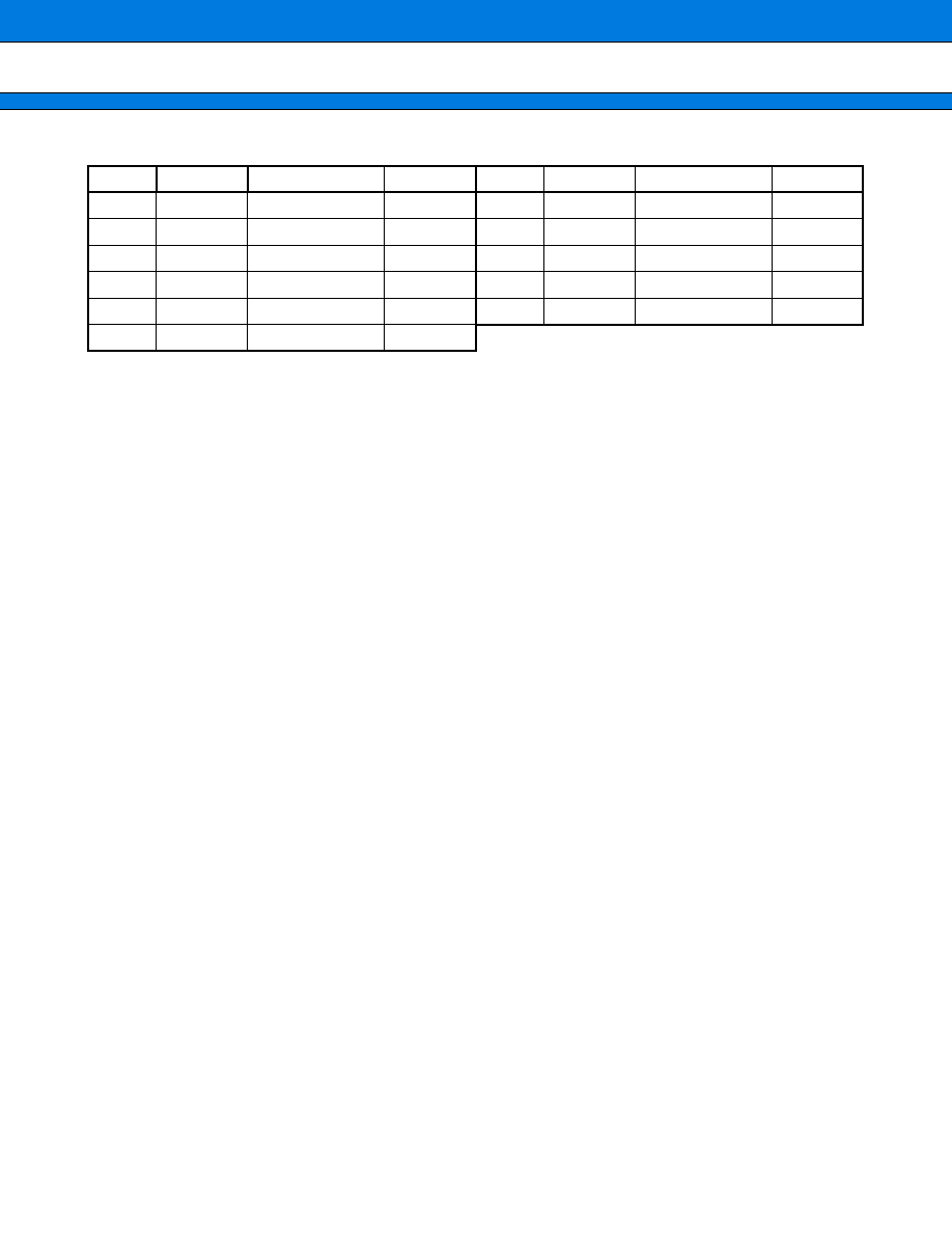
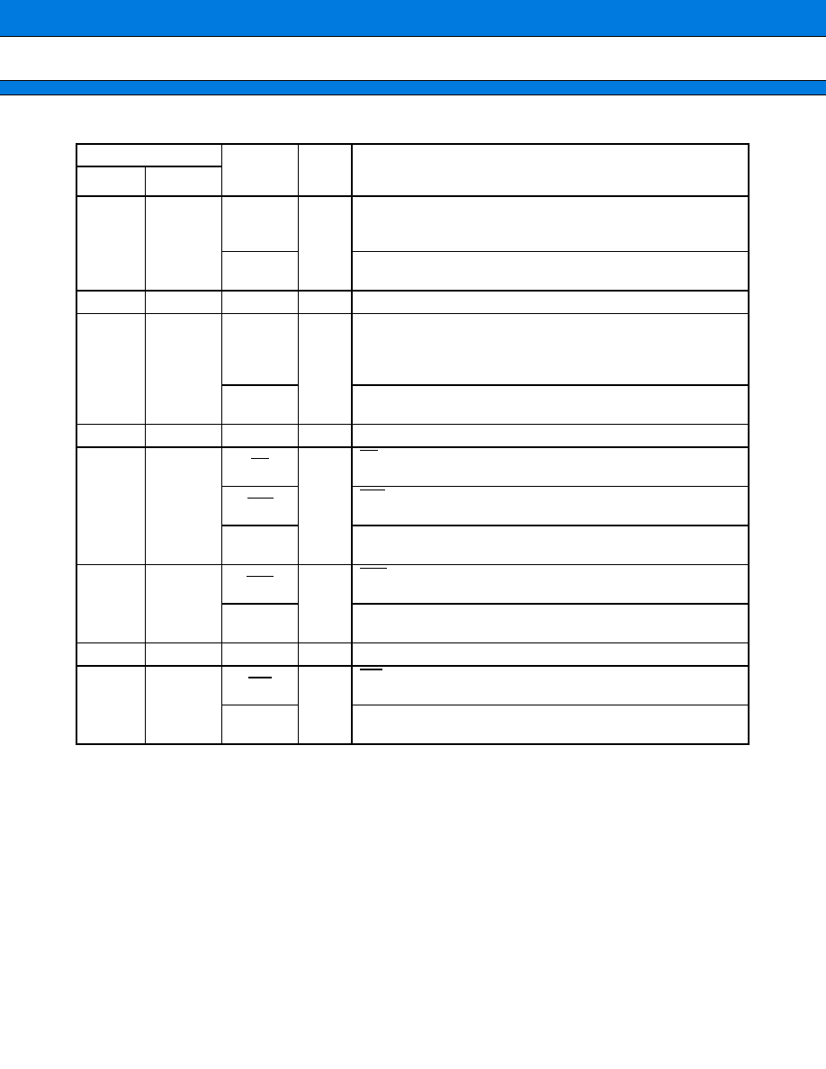
PRODUCT LINEUP
Note : I
2
C license
Purchase of Fujitsu I
2
C components conveys a license under the Philips I
2
C Patent rights to use
these components in an I
2
C system provided that the system conforms to the I
2
C Standard Specifi-
cation as defined by Philips.
MB91340
MB91V340
Type
MASK ROM version
(for volume production)
Evaluation version
(For evaluation and development)
Max external bus width
16-bit
32-bit
Max no. of ports
107
125
(additional ports are P00 to P07, P10 to
P17, P86, P87)
Write strobe
WR0 to WR1
WR0 to WR3
RAM
112 KB
128 KB
ROM
64 KB mask ROM
64 KB emulation RAM
Instruction cache
None
4 KB
Package
LQFP-176
PGA-361
Other
Currently in production
Currently available
MB91340/MB91V340
5
s
s
s
s
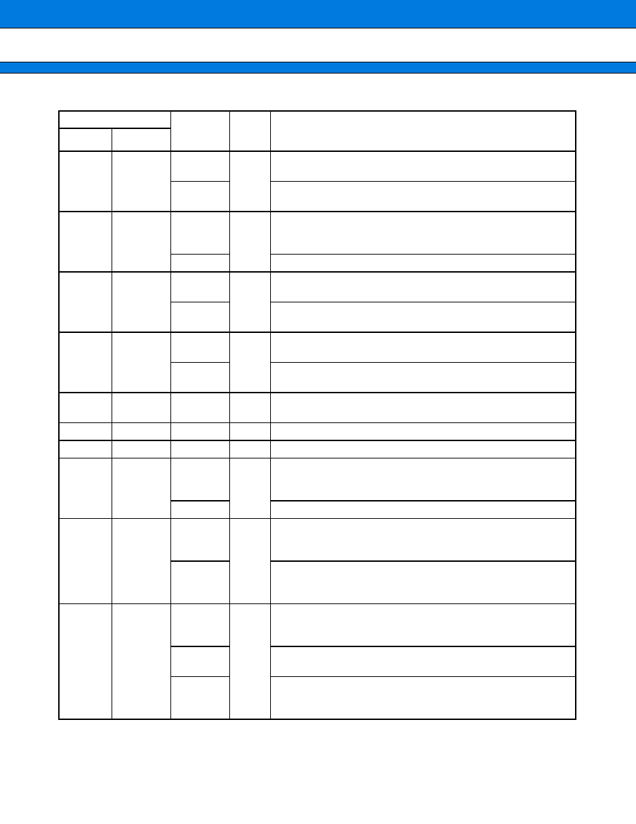
PIN ASSIGNMENTS
∑ MB91340
(TOP VIEW)
(FPT-176P-M02)
133
134
135
136
137
138
139
140
141
142
143
144
145
146
147
148
149
150
151
152
153
154
155
156
157
158
159
160
161
162
163
164
165
166
167
168
169
170
171
172
173
174
175
176
V
SS
X1
X0
V
CC
3
PC0/DREQ2
PC1/DACK2
PC2/DSTP2/DEOP2
PB0/DREQ0
PB1/DACK0
PB2/DSTP0/DEOP0
PB3/DREQ1
PB4/DACK1
PB5/DSTP1/DEOP1
PB6/IOWR
PB7/IORD
V
SS
PA0/CS0
PA1/CS1
PA2/CS2
PA3/CS3
PA4/CS4
PA5/CS5
PA6/CS6
PA7/CS7
V
CC
3
V
CC
2
NMI
HST
INIT
P80/RDY
P81/BGRNT
P82/BRQ
RD
WR0/UUB
P85/WR1/ULB
V
SS
P90/SYSCLK
P91
P92/MCLK
P93
P94/AS/LBA
P95/BAA
P96
P97/WR
1 2 3 4 5 6 7 8 9 10 11 12 13 14 15 16 17 18 19 20 21 22 23 24 25 26 27 28 29 30 31 32 33 34 35 36 37 38 39 40 41 42 43 44
P20/D16 P21/D17 P22/D18 P23/D19 P24/D20 P25/D21 P26/D22 P27/D23
D24 D25 D26 D27 D28 D29 D30 D31 V
SS
A00 A01 A02 A03 A04 A05 A06 A07
V
CC
3
V
CC
2
A08 A09 A10 A11 A12 A13 A14 A15 V
SS
P60/A16 P61/A17 P62/A18 P63/A19 P64/A20 P65/A21 P66/A22 P67/A23
V
CC
2
V
SS
MD2 MD1 MD0 PH2/SCK2 PH1/SO2 PH0/SI2 PI5/SCK1 PI4/SO1 PI3/SI1 PI2/SCK0 PI1/SO0 PI0/SI0 PJ7/INT7 PJ6/INT6 PJ5/INT5 PJ4/INT4 PJ3/INT3 PJ2/INT2 PJ1/INT1 PJ0/INT0 V
CC
2
V
CC
3
PK7/TOT3 PK6/TOT2 PK5/TOT1 PK4/TOT0 PK3/TIN3 PK2/TIN2 PK1/TIN1 PK0/TIN0 V
SS
PL6/UCO PL5 PL4 PL3/SCLO PL2/SCL/SCLI PL1/SDAO PL0/SDA/SDAI PM3/ZIN3 PM2/ZIN2 PM1/ZIN1 PM0/ZIN0
132 131 130 129 128 127 126 125 124 123 122 121 120 119 118 117 116 115 114 113 112 111 110 109 108 107 106 105 104 103 102 101 100
99 98 97 96 95 94 93 92 91 90 89
PN7/BIN3
PN6/AIN3
PN5/BIN2
PN4/AIN2
PN3/BIN1
PN2/AIN1
PN1/BIN0
PN0/AIN0
V
SS
PO7/OC7
PO6/OC6
PO5/OC5
PO4/OC4
PO3/OC3
PO2/OC2
PO1/OC1
PO0/OC0
V
CC
2
V
CC
3
PP7
PP6
PP5/IN3
PP4/IN2
PP3/IN1
PP2/IN0
PP1/FRCK
PP0/ATG
V
SS
AV
SS
/AVRL
AVRH
AV
CC
AN7
AN6
AN5
AN4
AN3
AN2
AN1
AN0
DA2
DA1
DA0
DAVC
DAVS
88
87
86
85
84
83
82
81
80
79
78
77
76
75
74
73
72
71
70
69
68
67
66
65
64
63
62
61
60
59
58
57
56
55
54
53
52
51
50
49
48
47
46
45
MB91340/MB91V340
6
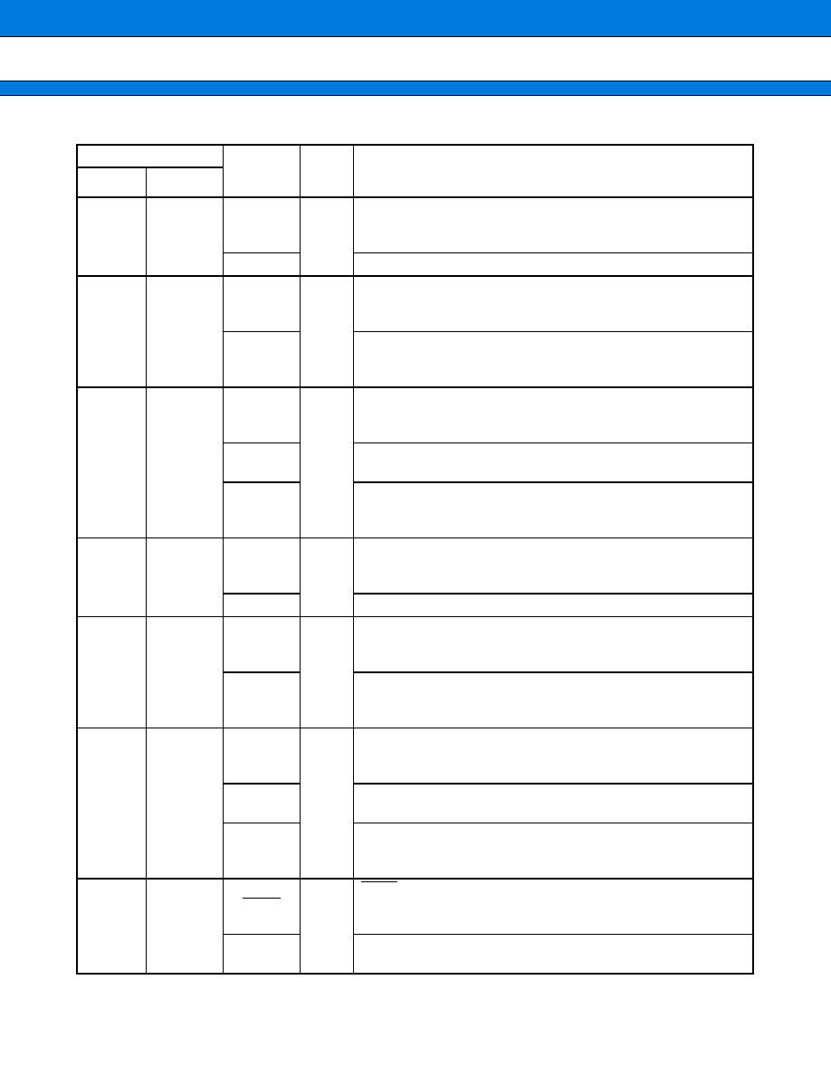
∑ MB91V340
Note : Operation of 32-bit bus pins P00/D00 to P17/D15, P86/WR2 and P87/WR3 is not currently guaranteed.
(BOTTOM VIEW)
(PGA-361C-A01)
Index
35
34
33
32
31
30
29
28
27
26
25
24
23
22
21
20
19
18
17
16
15
14
13
12
11
10
9
8
7
6
5
4
3
2
1
AR
AP
AN
AM
AL
AK
AJ
AH
AG
AF
AE
AD
AC
AB
AA
Y W V U T R P N M L K J H G F E D C B A

MB91340/MB91V340
7
s
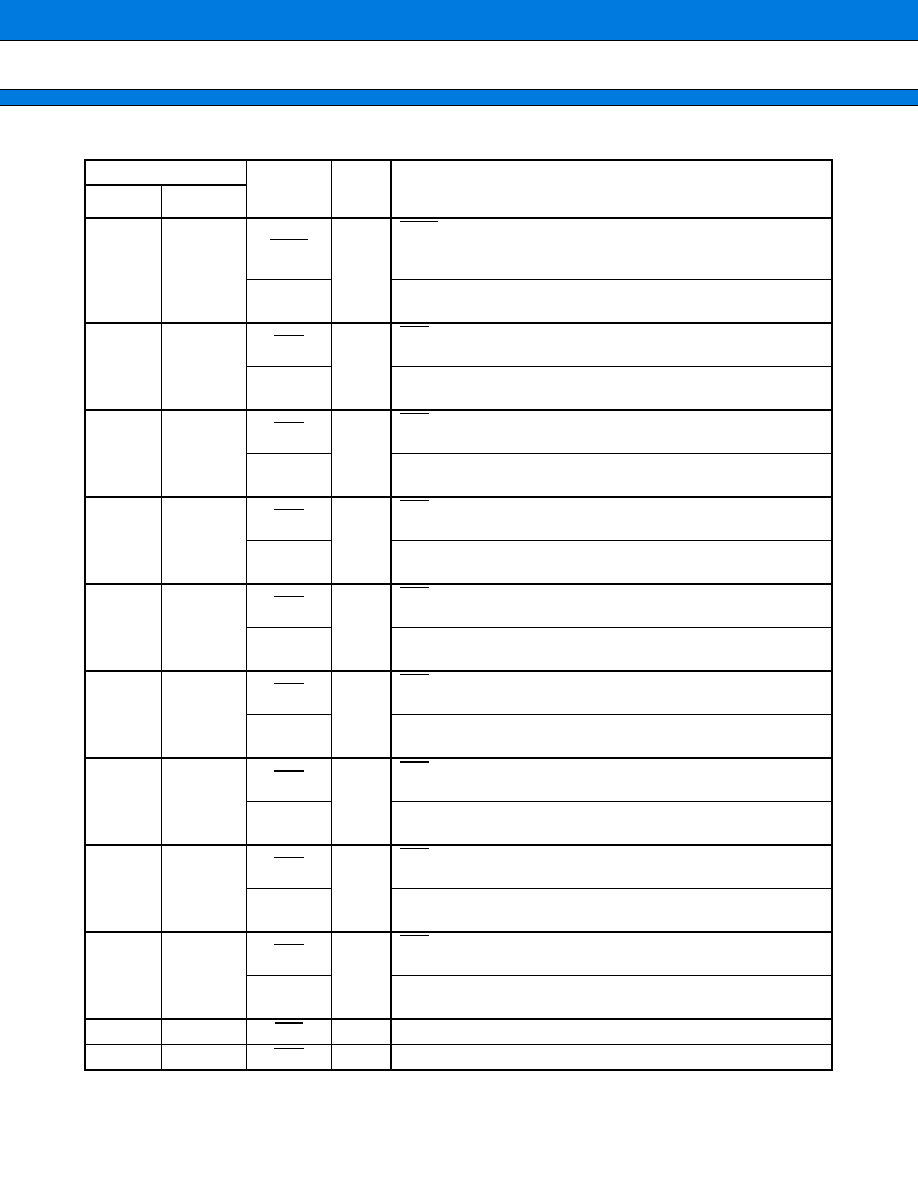
PIN NO. TABLE
∑ Device : MB91V340 Package : PGA-361C-A01
(Continued)
No.
PIN
Pin Name
Remarks
No.
PIN
Pin Name
Remarks
1
F6
P13/D11
V340
36
G17
V
CC
2
2
C5
P14/D12
V340
37
A15
A08
3
E7
P15/D13
V340
38
D16
A09
4
G7
V
SS
39
E17
A10
5
F8
P16/D14
V340
40
B16
A11
6
D6
P17/D15
V340
41
F18
A12
7
G9
V
CC
2
42
D18
A13
8
B6
P20/D16
43
C17
A14
9
C7
P21/D17
44
G19
V
SS
10
F10
P22/D18
45
A17
A15
11
E9
P23/D19
46
E19
P60/A16
12
D8
P24/D20
47
B20
P61/A17
13
G11
V
SS
48
B18
P62/A18
14
A9
P25/D21
49
D20
P63/A19
15
F12
P26/D22
50
C19
P64/A20
16
B8
P27/D23
51
F20
V
CC
3
17
C11
D24
52
A19
P65/A21
18
C9
D25
53
E21
P66/A22
19
A11
D26
54
G21
V
SS
20
E11
D27
55
C21
P67/A23
21
F14
V
CC
3
56
A21
EX_A23
V340
22
E13
D28
57
F22
DAVS
23
G13
V
SS
58
D22
DAVC
24
D12
D29
59
B22
DA0
25
D10
D30
60
B24
DA1
26
C13
D31
61
C23
DA2
27
B10
A00
62
D24
AN0
28
E15
A01
63
E23
AN1
29
B12
A02
64
G23
V
SS
30
D14
A03
65
A23
AN2
31
B14
A04
66
G25
V
CC
2
32
A13
A05
67
A25
AN3
33
G15
V
SS
68
B26
AN4
34
F16
A06
69
F24
AN5
35
C15
A07
70
D26
AN6
MB91340/MB91V340
8
(Continued)
No.
PIN
Pin Name
Remarks
No.
PIN
Pin Name
Remarks
71
C25
AN7
106
L33
PM1/ZIN1
72
B28
AV
CC
107
M30
V
CC
3
73
E25
AVRH
108
L35
PM2/ZIN2
74
G27
V
SS
109
N29
V
SS
75
A27
AVRL/AV
SS
110
M32
PM3/ZIN3
76
C27
PP0/ATG
111
M34
PL0/SDA/SDAI
77
E27
PP1/FRCK
112
N31
PL1/SDAO
78
D28
PP2/IN0
113
P32
PL2/SCL/SCLI
79
C29
PP3/IN1
114
N33
PL3/SCLO
80
F26
V
CC
3
115
P34
PL4
81
D30
PP4/IN2
116
P30
PL5
82
B30
PP5/IN3
117
T32
PL6/UCO
83
F28
V
SS
118
N35
PK0/TIN0
84
E29
PP6
119
R29
V
SS
85
C31
PP7
120
R31
PK1/TIN1
86
E31
PO0/OC0
121
R33
PK2/TIN2
87
F30
PO1/OC1
122
U29
V
CC
2
88
E33
PO2/OC2
123
T30
PK3/TIN3
89
G31
PO3/OC3
124
T34
PK4/TOT0
90
G29
V
SS
125
R35
PK5/TOT1
91
H30
PO4/OC4
126
V34
PK6/TOT2
92
F32
PO5/OC5
127
U33
PK7/TOT3
93
J29
V
CC
2
128
V32
PJ0/INT0
94
F34
PO6/OC6
129
U31
PJ1/INT1
95
H32
PO7/OC7
130
W29
V
SS
96
J31
PN0/AIN0
131
U35
PJ2/INT2
97
H34
PN1/BIN0
132
V30
PJ3/INT3
98
K30
PN2/AIN1
133
Y34
PJ4/INT4
99
L29
V
SS
134
W35
PJ5/INT5
100
G33
PN3/BIN1
135
Y32
PJ6/INT6
101
J33
PN4/AIN2
136
W33
PJ7/INT7
102
K32
PN5/BIN2
137
Y30
V
CC
3
103
L31
PN6/AIN3
138
W31
PI0/SI0
104
K34
PN7/BIN3
139
AA35
PI1/SO0
105
J35
PM0/ZIN0
140
AA29
V
SS
MB91340/MB91V340
9
(Continued)
No.
PIN
Pin Name
Remarks
No.
PIN
Pin Name
Remarks
141
AA33
PI2/SCK0
176
AJ29
V
SS
142
AB34
PI3/SI1
177
AK28
TDT45
V340
143
AC35
PI4/SO1
178
AM30
TDT44
V340
144
AB32
PI5/SCK1
179
AJ27
V
CC
2
145
AA31
PH0/SI2
180
AP30
TDT43
V340
146
AD34
PH1/SO2
181
AN29
TDT42
V340
147
AC33
PH2/SCK2
182
AK26
TDT41
V340
148
AD32
TDT68
V340
183
AL27
TDT40
V340
149
AE35
TDT67
V340
184
AM28
TDT39
V340
150
AC29
V
SS
185
AJ25
V
SS
151
AB30
TDT66
V340
186
AR27
TDT38
V340
152
AD30
V
CC
2
187
AK24
TDT37
V340
153
AC31
TDT65
V340
188
AP28
TDT36
V340
154
AF34
TDT64
V340
189
AN25
TDT35
V340
155
AE33
TDT63
V340
190
AN27
TDT34
V340
156
AF32
TDT62
V340
191
AR25
TDT33
V340
157
AG35
TDT61
V340
192
AL25
TDT32
V340
158
AH34
TDT60
V340
193
AK22
V
CC
3
159
AE31
TDT59
V340
194
AL23
TDT31
V340
160
AG29
V
SS
195
AJ23
V
SS
161
AG33
TDT58
V340
196
AM24
TDT30
V340
162
AH32
TDT57
V340
197
AM26
TDT29
V340
163
AG31
TDT56
V340
198
AN23
TDT28
V340
164
AF30
TDT55
V340
199
AP26
TDT27
V340
165
AJ33
TDT54
V340
200
AL21
TDT26
V340
166
AE29
V
CC
3
201
AP24
TDT25
V340
167
AK32
TDT53
V340
202
AM22
TDT24
V340
168
AK34
TDT52
V340
203
AP22
TDT23
V340
169
AH30
V
SS
204
AR23
TDT22
V340
170
AJ31
TDT51
V340
205
AJ21
V
SS
171
AL33
TDT50
V340
206
AK20
TDT21
V340
172
AL31
TDT49
V340
207
AN21
TDT20
V340
173
AK30
TDT48
V340
208
AJ19
V
CC
2
174
AN31
TDT47
V340
209
AR21
TDT19
V340
175
AL29
TDT46
V340
210
AM20
TDT18
V340
MB91340/MB91V340
10
(Continued)
No.
PIN
Pin Name
Remarks
No.
PIN
Pin Name
Remarks
211
AL19
TDT17
V340
246
AJ9
V
SS
212
AP20
TDT16
V340
247
AR9
TAD08
V340
213
AK18
TDT15
V340
248
AN9
TAD07
V340
214
AM18
TDT14
V340
249
AL9
TAD06
V340
215
AN19
TDT13
V340
250
AM8
TAD05
V340
216
AJ17
V
SS
251
AN7
TAD04
V340
217
AR19
TDT12
V340
252
AK10
V
CC
3
218
AL17
TDT11
V340
253
AM6
TAD03
V340
219
AP16
TDT10
V340
254
AP6
TAD02
V340
220
AP18
TDT09
V340
255
AK8
V
SS
221
AM16
TDT08
V340
256
AL7
TAD01
V340
222
AN17
TDT07
V340
257
AN5
TAD00
V340
223
AK16
V
CC
3
258
AL5
EXRAM
V340
224
AR17
TDT06
V340
259
AK6
BREAK
225
AL15
TDT05
V340
260
AL3
ICD3
V340
226
AJ15
V
SS
261
AJ5
ICD2
V340
227
AN15
TDT04
V340
262
AJ7
V
SS
228
AR15
TDT03
V340
263
AH6
ICD1
V340
229
AK14
TDT02
V340
264
AK4
ICD0
V340
230
AM14
TDT01
V340
265
AG7
V
CC
2
231
AP14
TDT00
V340
266
AK2
ICS2
V340
232
AP12
TWR
V340
267
AH4
ICS1
V340
233
AN13
TADSC
V340
268
AG5
ICS0
V340
234
AM12
TCE1
V340
269
AH2
ICLK
V340
235
AL13
TOE
V340
270
AF6
RST
V340
236
AJ13
V
SS
271
AE7
V
SS
237
AR13
TCLK
V340
272
AJ3
MD0
238
AJ11
V
CC
2
273
AG3
MD1
239
AR11
TAD15
V340
274
AF4
MD2
240
AP10
TAD14
V340
275
AE5
V
CC
2
V340
241
AK12
TAD13
V340
276
AF2
OPEN
V340
242
AM10
TAD12
V340
277
AG1
OPEN
V340
243
AN11
TAD11
V340
278
AE3
OPEN
V340
244
AP8
TAD10
V340
279
AD6
V
CC
3
245
AL11
TAD09
V340
280
AE1
X0
MB91340/MB91V340
11
(Continued)
No.
PIN
Pin Name
Remarks
No.
PIN
Pin Name
Remarks
281
AC7
V
SS
316
P4
RD
282
AD4
X1
317
R5
WR0/UUB
283
AD2
PC0/DREQ2
318
M2
P85/WR1/ULB
284
AC5
V
CC
2
V340
319
N3
P86/WR2/LUB
V340
285
AB4
PC1/DACK2
320
M4
P87/WR3/LLB
V340
286
AC3
PC2/DSTP2/
DEOP2
321
L1
P90/SYSCLK
287
AB2
PB0/DREQ0
322
N7
V
SS
288
AB6
PB1/DACK0
323
P6
P91
289
Y4
PB2/DSTP0/
DEOP0
324
M6
V
CC
2
290
AC1
PB3/DREQ1
325
N5
P92/MCLK
291
AA7
V
SS
326
K2
P93
292
AA5
PB4/DACK1
327
L3
P94/AS/LBA
293
AA3
PB5/DSTP1/
DEOP1
328
K4
P95/BAA
294
W7
V
CC
2
329
J1
P96
295
Y6
PB6/IOWR
330
H2
P97/WR
296
Y2
PB7/IORD
331
L5
P00/D00
V340
297
AA1
PA0/CS0
332
J7
V
SS
298
V2
PA1/CS1
333
J3
P01/D01
V340
299
W3
PA2/CS2
334
H4
P02/D02
V340
300
V4
PA3/CS3
335
J5
P03/D03
V340
301
W5
PA4/CS4
336
K6
P04/D04
V340
302
U7
V
SS
337
G3
P05/D05
V340
303
W1
PA5/CS5
338
L7
V
CC
3
304
V6
PA6/CS6
339
F4
P06/D06
V340
305
T2
PA7/CS7
340
F2
P07/D07
V340
306
U1
NMI
341
H6
V
SS
307
T4
HST
342
G5
P10/D08
V340
308
U3
INIT
343
E3
P11/D09
V340
309
T6
V
CC
3
344
E5
P12/D10
V340
310
U5
EX_BGRNT
V340
345
A7
OPEN
V340
311
R1
EX_BRQ
V340
346
A29
OPEN
V340
312
R7
V
SS
347
B2
OPEN
V340
313
R3
P80/RDY
348
C3
OPEN
V340
314
P2
P81/BGRNT
349
C33
OPEN
V340
315
N1
P82/BRQ
350
D4
OPEN
V340
MB91340/MB91V340
12
(Continued)
Note : Pins with "V340" in the "Remarks" column are present on the MB91V340 only. They are not present on the
MB91340 mask ROM version.
No.
PIN
Pin Name
Remarks
No.
PIN
Pin Name
Remarks
351
D32
OPEN
V340
357
AM32
OPEN
V340
352
G1
OPEN
V340
358
AN3
OPEN
V340
353
G35
OPEN
V340
359
AN33
OPEN
V340
354
AJ1
OPEN
V340
360
AR7
OPEN
V340
355
AJ35
OPEN
V340
361
AR29
OPEN
V340
356
AM4
OPEN
V340
MB91340/MB91V340
13
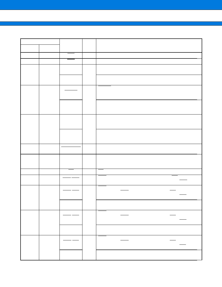
s
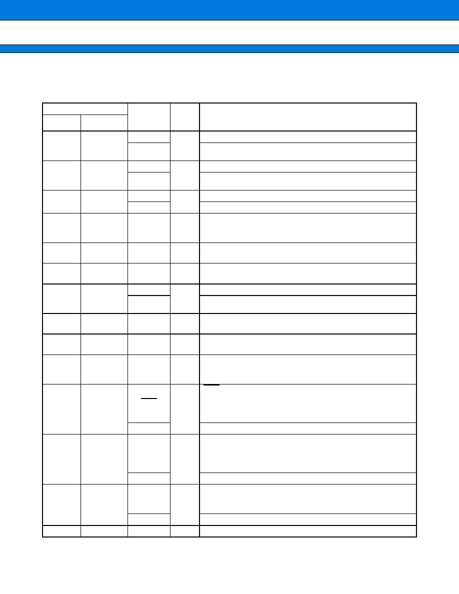
PIN DESCRIPTIONS
Refer to the Pin Assignment diagram. Pins used by the MB91V340 evaluation tools are not included in these
pin descriptions.
* : Shaded pins are only present on the MB91V340.
(Continued)
Pin no.
Pin name
I/O
circuit
type
Function
MB91340
MB91V340
331,
333 to 337,
339 to 340
D00 to D07
C
External data bus bits 0 to 7
*
P00 to P07
Can be used as ports in 8-bit or 16-bit external bus mode.
*
342 to 344,
1 to 3,
5 to 6
D08 to D15
C
External data bus bits 08 to 15
*
P10 to P17
Can be used as ports in 8-bit or 16-bit external bus mode.
*
1 to 8
8 to 12,
14 to 16
D16 to D23
C
External data bus bits 16 to 23
P20 to P27
Can be used as ports in 8-bit external bus mode.
9 to 16
17 to 20,
22,
24 to 26
D24 to D31
C
External data bus bits 24 to 31
18 to 25
27 to 32,
34 to 35
A00 to A07
C
External address bus bits 0 to 7
28 to 35
37 to 43,
45
A08 to A15
C
External address bus bits 8 to 15
37 to 44
46 to 50,
52 to 53,
55
A16 to A23
C
External address bus bits 16 to 23
P60 to P67
Can be used as ports when external address bus not used.
56
EX_A23
J
External address bus bit 23. This outputs the status of the
internal bus.
*
47 to 49
59 to 61
DA0 to
DA2
D/A converter output pins
50 to 57
62 to 63,
65,
67 to 71
AN0 to
AN7
D
Analog input pins
62
76
ATG
C
[ATG] External trigger input for A/D converter. This input is
used continuously when selected as the A/D converter start
trigger. In this case, do not output to this port unless doing so
intentionally.
PP0
[PP0] General purpose input/output port.
63
77
FRCK
C
[FRCK] External clock input pin for freerun timer. This input is
used continuously when selected as the external clock input
pin for the freerun timer. In this case, do not output to this port
unless doing so intentionally.
PP1
[PP1] General purpose input/output pin.
64 to 67
78 to 79,
81 to 82
IN0 to IN3
C
[IN0-IN3] Input capture input pin. These inputs are used con-
tinuously when selected as input capture inputs. In this case,
do not output to these ports unless doing so intentionally.
PP2 to PP5
[PP2-PP5] General purpose input/output ports.
68 to 69
84 to 85
PP6 to PP7
C
[PP6-PP7] General purpose input/output ports.
MB91340/MB91V340
14
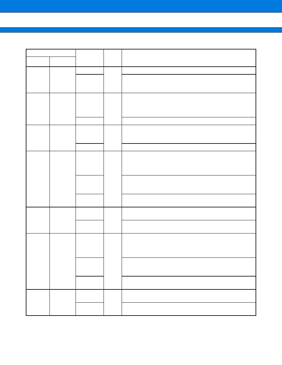
* : Shaded pins are only present on the MB91V340.
(Continued)
Pin no.
Pin name
I/O
circuit
type
Function
MB91340 MB91V340
72 to 79
86 to 89,
91 to 92,
94 to 95
OC0 to OC7
C
[OC0-OC7] Output compare output pins.
PO0 to PO7
[PO0-PO7] General purpose input/output ports. These pins can
be used as ports when the output from the output compare unit is
not used.
81 to 88
96 to 98,
100 to 104
AIN0, BIN0,
AIN1, BIN1,
AIN2, BIN2,
AIN3, BIN3
C
[AIN0, BIN0, AIN1, BIN1, AIN2, BIN2, AIN3, BIN3] Up/down timer
inputs. These inputs are used continuously when input is en-
abled. In this case, do not output to these ports unless doing so
intentionally.
PN0 to PN7
[PN0-PN7] General purpose input/output ports.
89 to 92
105 to 106,
108,
110
ZIN0 to
ZIN3
C
[ZIN0-ZIN3] Up/down timer inputs. These inputs are used contin-
uously when input is enabled. In this case, do not output to these
ports unless doing so intentionally.
PM0 to PM3
[PM0-PM3] General purpose input/output ports.
93
111
SDA
C
[SDA] Data input/output pin for the I
2
C bus. The pin has this func-
tion when I
2
C is enabled in standard mode. In this case, do not
output to this port unless doing so intentionally. (Open drain out-
put)
SDAI
[SDAI] Data input pin for the I
2
C bus. The pin has this function
when I
2
C is enabled in terminal split mode. In this case, do not
output to this port unless doing so intentionally.
PL0
[PL0] General purpose input/output port. The pin operates as a
port when I
2
C operation is disabled.
94
112
SDAO
C
[SDAO] Data output pin for the I
2
C bus. The pin operates as a
dedicated data output when I
2
C is enabled in terminal split mode.
PL1
[PL1] General purpose input/output port. The pin operates as a
port when I
2
C terminal split mode operation is disabled.
95
113
SCL
C
[SCL] Clock input/output pin for the I
2
C bus. The pin has this func-
tion when I
2
C is enabled in standard mode. In this case, do not
output to this port unless doing so intentionally. (Open drain out-
put)
SCLI
[SCLI] Clock input pin for the I
2
C bus. The pin has this function
when I
2
C is enabled in terminal split mode. In this case, do not
output to this port unless doing so intentionally.
PL2
[PL2] General purpose input/output port. The pin operates as a
port when I
2
C operation is disabled.
96
114
SCLO
C
[SCLO] Clock output pin for the I
2
C bus. The pin is used as the
clock output when I
2
C is enabled in terminal split mode.
PL3
[PL3] General purpose input/output port. The pin operates as a
port when I
2
C terminal split mode operation is disabled.
MB91340/MB91V340
15
* : Shaded pins are only present on the MB91V340.
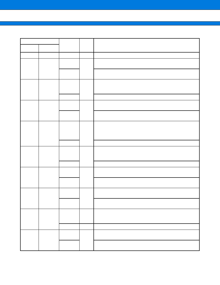
(Continued)
Pin no.
Pin name
I/O
circuit
type
Function
MB91340 MB91V340
97 to 98
115 to 116 PL4 to PL5
C
[PL4-PL5] General purpose input/output ports.
99
117
UCO
C
[UCO] Pulse output for 8-bit up counter. The pin outputs pulses
when pulse output is enabled for the 8-bit up counter.
PL6
[PL6] General purpose input/output port. The pin operates as a
port when output is disabled for the 8-bit up counter.
101 to
104
118,
120 to 121,
123
TIN0 to
TIN3
C
[TIN0-TIN3] Reload timer inputs. These inputs are used continu-
ously when the corresponding timer input is enabled. In this case,
do not output to these ports unless doing so intentionally.
PK0 to PK3
[PK0-PK3] General purpose input/output ports.
105 to
108
124 to 127
TOT0 to
TOT3
C
[TOT0-TOT3] Reload timer output ports. The pins operate as re-
load timer output ports when timer output is enabled.
PK4 to PK7
[PK4-PK7] General purpose input/output ports. The pins operate
as ports when timer output is disabled.
111 to
118
128 to 129,
131 to 136
INT0 to
INT7
I
[INT0-INT7] External interrupt inputs. These inputs are used con-
tinuously when the corresponding external interrupt is enabled. In
this case, do not output to these ports unless doing so intentional-
ly.
PJ0 to PJ7
[PJ0-PJ7] General purpose input/output ports.
119
138
SI0
C
[SI0] UART0 data input pin. This input is used continuously when
UART0 is performing input. In this case, do not output to this port
unless doing so intentionally.
PI0
[PI0] General purpose input/output port.
120
139
SO0
C
[SO0] UART0 data output pin. The pin has this function when
UART0 data output is enabled.
PI1
[PI1] General purpose input/output port. The pin has this function
when UART0 data output is disabled.
121
141
SCK0
C
[SCK0] UART0 clock input/output pin. The pin has this function
when UART0 clock output is enabled.
PI2
[PI2] General purpose input/output port. The pin has this function
when UART0 clock output is disabled.
122
142
SI1
C
[SI1] UART1 data input pin. This input is used continuously when
UART1 is performing input. In this case, do not output to this port
unless doing so intentionally.
PI3
C
[PI3] General purpose input/output port.
123
143
SO1
C
[SO1] UART1 data output pin. The pin has this function when
UART1 data output is enabled.
PI4
[PI4] General purpose input/output port. The pin has this function
when UART1 data output is disabled.
MB91340/MB91V340
16
* : Shaded pins are only present on the MB91V340.
(Continued)
Pin no.
Pin name
I/O
circuit
type
Function
MB91340 MB91V340
124
144
SCK1
C
[SCK1] UART1 clock input/output pin. The pin has this function
when UART1 clock output is enabled.
PI5
[PI5] General purpose input/output port. The pin has this function
when UART1 clock output is disabled.
125
145
SI2
C
[SI2] UART2 data input pin. This input is used continuously when
UART2 is performing input. In this case, do not output to this port
unless doing so intentionally.
PH0
[PH0] General purpose input/output port.
126
146
SO2
C
[SO2] UART1 data output pin. The pin has this function when
UART2 data output is enabled.
PH1
[PH1] General purpose input/output port. The pin has this function
when UART2 data output is disabled.
127
147
SCK2
C
[SCK2] UART2 clock input/output pin. The pin has this function
when UART2 clock output is enabled.
PH2
[PH2] General purpose input/output port. The pin has this function
when UART2 clock output is disabled.
128 to
130
272 to 274
MD0 to
MD2
G
[MD0-MD2] Mode pins 0 to 2. The levels applied to these pins set
the basic operating mode. Connect to VCC or VSS.
134
282
X1
A
Clock (oscillation) output
135
280
X0
A
Clock (oscillation) input
137
283
DREQ2
C
[DREQ2] External input for DMA transfer requests. This input is
used continuously when selected as a DMA activation trigger. In
this case, do not output to this port unless doing so intentionally.
PC0
[PC0] General purpose input/output port.
138
285
DACK2
C
[DACK2] External acknowledge output for DMA transfer requests.
The pin has this function when outputting DMA transfer request
acknowledgement is enabled.
PC1
[PC1] General purpose input/output port. The pin has this function
when outputting DMA transfer request acknowledgement is dis-
abled.
139
286
DEOP2
C
[DEOP2] Completion output for DMA external transfer. The pin
has this function when outputting DMA transfer completion is en-
abled.
DSTP2
[DSTP2] Stop input for DMA external transfer. The pin has this
function when the stop input is enabled for DMA transfer.
PC2
[PC2] General purpose input/output port. The pin has this function
when completion output and stop input are disabled for DMA
transfer.
MB91340/MB91V340
17
* : Shaded pins are only present on the MB91V340.
(Continued)
Pin no.
Pin name
I/O
circuit
type
Function
MB91340 MB91V340
140
287
DREQ0
C
[DREQ0] External input for DMA transfer requests. This input is
used continuously when selected as a DMA activation trigger. In
this case, do not output to this port unless doing so intentionally.
PB0
[PB0] General purpose input/output port.
141
288
DACK0
C
[DACK0] External acknowledge output for DMA transfer requests.
The pin has this function when outputting DMA transfer request
acknowledgement is enabled.
PB1
[PB1] General purpose input/output port. The pin has this function
when outputting DMA transfer request acknowledgement is dis-
abled.
142
289
DEOP0
C
[DEOP0] Completion output for DMA external transfer. The pin
has this function when outputting DMA transfer completion is en-
abled.
DSTP0
[DSTP0] Stop input for DMA external transfer. The pin has this
function when the stop input is enabled for DMA transfer.
PB2
[PB2] General purpose input/output port. The pin has this function
when completion output and stop input are disabled for DMA
transfer.
143
290
DREQ1
C
[DREQ1] DMA External input for DMA transfer requests. This input
is used continuously when selected as a DMA activation trigger. In
this case, do not output to this port unless doing so intentionally.
PB3
[PB3] General purpose input/output port.
144
292
DACK1
C
[DACK1] External acknowledge output for DMA transfer requests.
The pin has this function when outputting DMA transfer request
acknowledgement is enabled.
PB4
[PB4] General purpose input/output port. The pin has this function
when outputting DMA transfer request acknowledgement is dis-
abled.
145
293
DEOP1
C
[DEOP1] Completion output for DMA external transfer. The pin
has this function when outputting DMA transfer completion is en-
abled.
DSTP1
[DSTP1] Stop input for DMA external transfer. The pin has this
function when the stop input is enabled for DMA transfer.
PB5
[PB5] General purpose input/output port. The pin has this function
when completion output and stop input are disabled for DMA
transfer.
146
295
IOWR
C
[IOWR] Write strobe output for DMA fly-by transfer. The pin has
this function when outputting a write strobe for DMA fly-by transfer
is enabled.
PB6
[PB6] General purpose input/output port. The pin has this function
when outputting a write strobe for DMA fly-by transfer is disabled.
MB91340/MB91V340
18
* : Shaded pins are only present on the MB91V340.
(Continued)
Pin no.
Pin name
I/O
circuit
type
Function
MB91340 MB91V340
147
296
IORD
C
[IORD] Read strobe output for DMA fly-by transfer. The pin has
this function when outputting a read strobe for DMA fly-by transfer
is enabled.
PB7
[PB7] General purpose input/output port. The pin has this function
when outputting a read strobe for DMA fly-by transfer is disabled.
149
297
CS0
C
[CS0] Chip select 0 output. The pin has this function when chip se-
lect 0 output is enabled.
PA0
[PA0] General purpose input/output port. The pin has this function
when chip select 0 output is disabled.
150
298
CS1
C
[CS1] Chip select 1 output. The pin has this function when chip se-
lect 1 output is enabled.
PA1
[PA1] General purpose input/output port. The pin has this function
when chip select 1 output is disabled.
151
299
CS2
C
[CS2] Chip select 2 output. The pin has this function when chip se-
lect 2 output is enabled.
PA2
[PA2] General purpose input/output port. The pin has this function
when chip select 2 output is disabled.
152
300
CS3
C
[CS3] Chip select 3 output. The pin has this function when chip se-
lect 3 output is enabled.
PA3
[PA3] General purpose input/output port. The pin has this function
when chip select 3 output is disabled.
153
301
CS4
C
[CS4] Chip select 4 output. The pin has this function when chip se-
lect 4 output is enabled.
PA4
[PA4] General purpose input/output port. The pin has this function
when chip select 4 output is disabled.
154
303
CS5
C
[CS5] Chip select 5 output. The pin has this function when chip se-
lect 5 output is enabled.
PA5
[PA5] General purpose input/output port. The pin has this function
when chip select 5 output is disabled.
155
304
CS6
C
[CS6] Chip select 6 output. The pin has this function when chip se-
lect 6 output is enabled.
PA6
[PA6] General purpose input/output port. The pin has this function
when chip select 6 output is disabled.
156
305
CS7
C
[CS7] Chip select 7 output. The pin has this function when chip se-
lect 7 output is enabled.
PA7
[PA7] General purpose input/output port. The pin has this function
when chip select 7 output is disabled.
159
306
NMI
G
NMI (Non Maskable Interrupt) input
160
307
HST
G
Hardware standby input
MB91340/MB91V340
19
* : Shaded pins are only present on the MB91V340.
(Continued)
Pin no.
Pin name
I/O
circuit
type
Function
MB91340 MB91V340
161
308
INIT
B
External reset input (Reset to initialize settings)
270
RST
B
External reset input (Reset to initialize operation)
*
162
313
RDY
C
[RDY] External ready input. The pin has this function when
external ready input is enabled.
P80
[P80] General purpose input/output port. The pin has this
function when external ready input is disabled.
163
314
BGRNT
C
[BGRNT] Acknowledge output for external bus release.
Outputs "L" when the external bus is released. The pin has this
function when output is enabled.
P81
[P81] General purpose input/output port. The pin has this
function when output is disabled for external bus release
acknowledge.
164
315
BRQ
C
[BRQ] External bus release request input. Input "1" to request
release of the external bus. The pin has this function when
input is enabled.
P82
[P82] General purpose input/output port. The pin has this
function when the external bus release request input is
disabled.
310
EX_BGRNT
J
Acknowledge output for external bus release. Outputs "L"
when the external bus is released.
*
311
EX_BRQ
K
External bus release request input. Input "1" to request release
of the external bus. The pin has this function when input is
enabled.
*
165
316
RD
C
[RD] External bus read strobe output.
166
317
WR0/UUB
C
[WR0] External bus write strobe output. When WR is used as
the write strobe, this becomes the byte-enable pin (UUB).
167
318
WR1/ULB
C
[WR1] External bus write strobe output. The pin has this
function when WR1 output is enabled. When WR is used as
the write strobe, this becomes the byte-enable pin (ULB).
P85
[P85] General purpose input/output port. The pin has this
function when the external bus write-enable output is disabled.
319
WR2/LUB
C
[WR2] External bus write strobe output. The pin has this
function when WR2 output is enabled. When WR is used as
the write strobe, this becomes the byte-enable pin (LUB).
*
P86
[P86] General purpose input/output port. The pin has this
function when the external bus write-enable output is disabled.
*
320
WR3/LLB
C
[WR3] External bus write strobe output. The pin has this
function when WR3 output is enabled. When WR is used as
the write strobe, this becomes the byte-enable pin (LLB).
*
P87
[P87] General purpose input/output port. The pin has this
function when the external bus write-enable output is disabled.
*
MB91340/MB91V340
20
(Continued)
* : Shaded pins are only present on the MB91V340.
Pin no.
Pin name
I/O
circuit
type
Function
MB91340 MB91V340
169
321
SYSCLK
C
[SYSCLK] System clock output. The pin has this function when
system clock output is enabled. This outputs the same clock as the
external bus operating frequency. (Output halts in stop mode.)
P90
[P90] General purpose input/output port. The pin has this function
when system clock output is disabled.
170
323
P91
C
[P91] General purpose input/output port.
171
325
MCLK
C
[MCLK] Memory clock output. The pin has this function when
memory clock output is enabled. This outputs the same clock as
the external bus operating frequency. (Output halts in sleep
mode.)
P92
[P92] General purpose input/output port. The pin has this function
when memory clock output is disabled.
172
326
P93
C
[P93] General purpose input/output port.
173
327
AS
C
[AS] Address strobe output. The pin has this function when ad-
dress strobe output is enabled.
LBA
[LBA] Address strobe output for burst flash ROM. The pin has this
function when address strobe output is enabled.
P94
[P94] General purpose input/output port. The pin has this function
when address strobe output is disabled.
174
328
BAA
C
[BAA] Address advance output for burst Flash ROM. The pin has
this function when address advance output is enabled.
P95
[P95] General purpose input/output port. The pin has this function
when address advance output is disabled.
175
329
P96
C
[P96] General purpose input/output port.
176
330
WR
C
[WR] Memory write strobe output. The pin has this function when
write strobe output is enabled.
P97
[P97] General purpose input/output port. The pin has this function
when write strobe output is disabled.
MB91340/MB91V340
21
[Power supply and GND pins]
Pin no.
Pin name
Function
MB91340
MB91V340
17, 36, 61, 80,
100,
131, 133, 148,
168
4, 23, 33, 44, 54, 64, 74, 83,
90, 99, 109, 119, 130, 140,
150, 160,
169, 176, 185, 195, 205,
216, 226, 236, 246, 255,
262, 271, 281,
291, 302, 312, 322, 332, 341
V
SS
GND pins.
Connect all pins at the same potential.
27, 71, 110, 132,
158
7, 36, 66, 93, 122, 179, 208,
238, 265, 275, 284, 294, 324
V
CC
2
2V power supply pins.
Connect all pins at the same potential.
26, 70, 109, 136,
157
21, 80, 107, 137, 166, 193,
223, 252, 279, 309, 338
V
CC
3
3V power supply pins.
Connect all pins at the same potential.
45
57
DAVS
GND pin for D/A converter
46
58
DAVC
Power supply pin for D/A converter
58
72
AV
CC
Analog power supply pin for A/D converter
59
73
AVRH
Reference power supply pin for A/D convert-
er
60
75
AV
SS
/AVRL
Analog GND pin for A/D converter
276, 277, 278, 345 to 361
OPEN
Open pins. Leave these pins open circuit.
MB91340/MB91V340
22
s
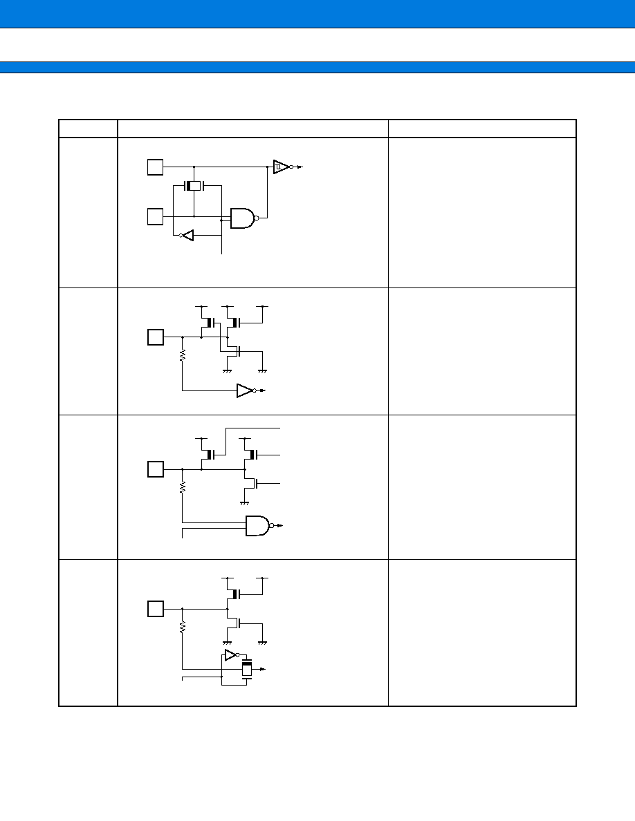
I/O CIRCUIT TYPE
(Continued)
Type
Circuit
Remarks
A
∑ Oscillation feedback resistance
approx. 1 M
B
∑ CMOS level input with pull-up
resistor
Pull-up resistor = 25 K
approx.
(Typ)
C
∑ CMOS level I/O with pull-up control
with standby control
Pull-up resistor = 25K
approx.
(Typ)
* : In I
2
C standard mode, the P-type
digital output is disabled and the pin
becomes an open drain output.
D
∑ Analog input
With switch
X1
STANDBY
CONTROL
X0
Pch
Nch
Clock input
R
Nch
Pch
Pch
V
SS
V
CC
3
Digital input
R
Nch
Pch
Pch
V
SS
V
CC
3
STANDBY CONTROL
Digital input
Digital output
Digital output
Pull-up control
R
Nch
Pch
Nch
CONTROL
Pch
V
SS
V
CC
3
Analog input
MB91340/MB91V340
23
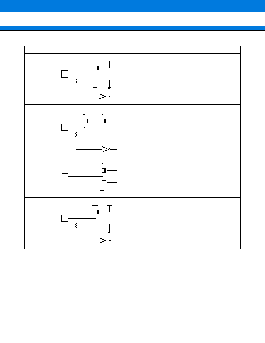
(Continued)
Type
Circuit
Remarks
G
∑ CMOS level input
No standby control
I
∑ CMOS level I/O with pull-up control
No standby control
Pull-up resistor
=
25 K
approx.
(Typ)
J
∑ CMOS level output
K
∑ CMOS level input with pull-down
Pull-down resistor
=
25 K
approx.
(Typ)
R
Nch
Pch
V
SS
V
CC
3
Digital input
R
Nch
Pch
Pch
V
SS
V
CC
3
Digital input
Digital output
Digital output
Pull-up control
Nch
Pch
V
SS
V
CC
3
Digital output
Digital output
R
Nch
Nch
Pch
V
SS
V
CC
3
Digital input

MB91340/MB91V340
24
s
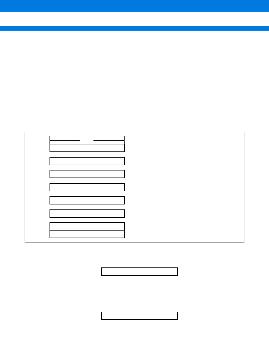
HANDLING DEVICES
∑
∑
∑
∑
Preventing Latchup
When CMOS integrated circuit devices are subjected to applied voltages higher than V
CC
3 at input and output
pins, or to voltages lower than V
SS
, as well as when voltages in excess of rated levels are applied between V
CC
3,
V
CC
2 and V
SS
, a phenomenon known as latchup can occur. When a latchup condition occurs, the supply current
can increase dramatically and may destroy semiconductor elements. In using semiconductor devices, always
take sufficient care to avoid exceeding maximum ratings.
∑
∑
∑
∑
Treatment of unused input pins
If unused input pins are left open, abnormal operation may result. Any unused input pins should be connected
to pull-up or pull-down resistors.
∑
∑
∑
∑
Power supply pins
Devices with multiple V
CC
3, V
CC
2 and V
SS
supply pins are designed to prevent problems such as latchup occurring
by providing internal connections between pins at the same potential. However, in order to reduce unwanted
radiation, prevent abnormal operation of strobe signals due to a rise in ground level, and to maintain the total
output current ratings, all such pins should always be connected externally to power supply or ground. Also,
ensure that the impedance of the V
CC
3, V
CC
2 and V
SS
connections to the power supply are as low as possible.
In addition, it is recommended that a bypass capacitor of approximately 0.1
µ
F be connected between V
CC
and
V
SS
. Connect the capacitor close to the V
CC
and V
SS
pins.
∑
∑
∑
∑
Crystal oscillators
Noise in proximity to the X0 and X1 pins can cause abnormal operation in this device. Printed circuit boards
should be designed so that the X0 and X1 pins, crystal (or ceramic) oscillator, and bypass capacitor connected
to ground are placed as close together as possible.
Also, to ensure stable operation, it is strongly recommended that the printed circuit board art work be designed
such that the X0 and X1 pins are surrounded by ground.
∑
∑
∑
∑
Treatment of NC and OPEN pins
Pins marked as "NC" or "OPEN" must be left open-circuit.
∑
∑
∑
∑
Mode pins (MD0 to MD2)
These pins should be connected directly to V
CC
3 or V
SS
. To prevent the device erroneously switching to test mode
due to noise, design the printed circuit board such that the distance between the mode pins and V
CC
3 or V
SS
is
as short as possible and the connection impedance is low.
∑
∑
∑
∑
Operation at startup
Always apply a settings initialization (INIT) to the INIT pin immediately after turning on the power.
Also, in order to provide a delay while the oscillator circuits stabilize immediately after startup, maintain the "L"
level input to the INIT pin for the required stabilization delay time. (The initialization processing (INIT) triggered
by the INIT pin initializes the oscillation stabilization delay time to the minimum setting.)
∑
∑
∑
∑
Source oscillation input at startup
At power-on startup, always input a clock signal until the oscillation stabilization delay time is ended.
MB91340/MB91V340
25
∑
∑
∑
∑
Hardware standby at power-on startup
If a hardware standby request occurs immediately after turning on the power, the settings initialization reset
(INIT) triggered by the INIT pin has priority. However, the device goes to the hardware standby state after the
settings initialization reset (INIT) triggered by the INIT pin completes. At this time, the oscillation stabilization
delay time is initialized to the maximum value and accordingly, this time is used for the oscillation stabilization
delay that occurs after hardware standby is released.
∑
∑
∑
∑
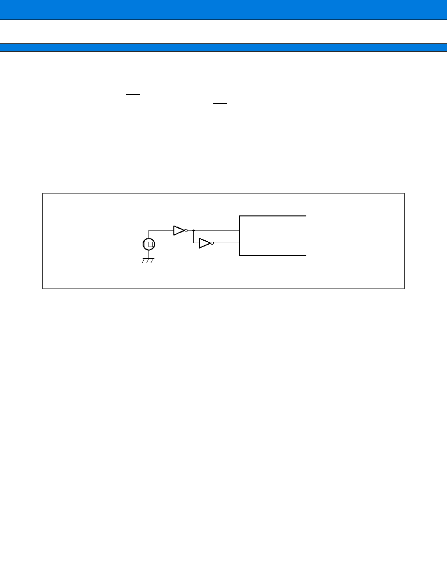
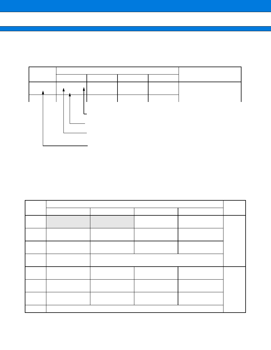
Remarks for External Clock Operation
When external clock is selected, supply it to X0 pin generally, and simultaneously the opposite phase clock to
X0 must be supplied to X1 pin. However, in this case the stop mode must not be used (because X1 pin stops at
"H" output in stop mode) .
X0
X1
MB91340/MB91V340
∑
∑
∑
∑
Using an external clock (normal)
Note: Stop mode (oscillation stop mode) can not be used.
MB91340/MB91V340
26
s
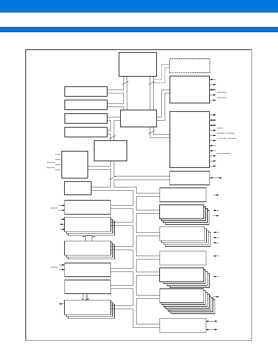
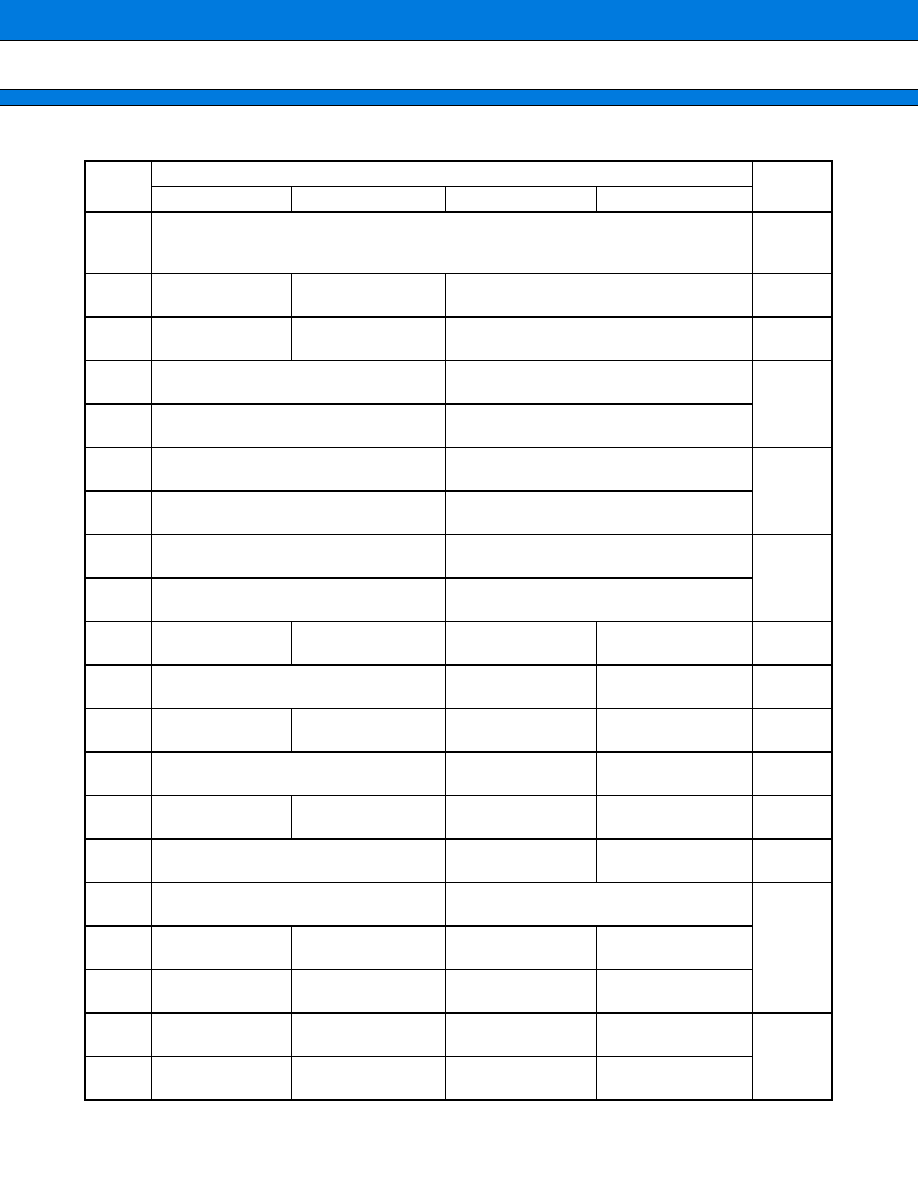
BLOCK DIAGRAM
(I-Cache 4 Kbytes)
DMAC 5 ch
PORT I/F
1 ch
I
2
C
FR CPU
Core
Bus
Converter
32
32
32
32
32 to 16
Adapter
ROM 64 Kbytes
RAM 112 Kbytes
(128 Kbytes)
16
3 ch
UART
3 ch
U-TIMER
8 ch
A/D
X0, X1
MD0-2
INIT
HST
INT0-7
NMI
SI0-2
SO0-2
SCK0-2
AN0-7
ATG
AVRH, AV
CC
AV
SS
/AVRL
DA0-2
DAVC, DAVS
DREQ0-2
DACK0-2
DEOP/DSTP0-2
IOWR
IORD
A23-00
D31-16
(D15-0)
RD
WR1, WR0
(WR2, WR3)
RDY
BRQ
BGRNT
SYSCLK
MCLK
PORT
UCO
FRCK
IN0-3
OC0-7
SDA
(SDAI/SDAO)
SCL
(SCLI/SCLO)
TIN0-3
TOT0-3
ZIN0-3
AIN0-3
BIN0-3
Bit search
RAM 4 Kbytes
(stack)
Clock
control
Interrupt
controller
8 ch
External interrupts
64 byte
◊
2 Waveform
data transfer
3 ch
Low speed D/A
8 ch
Output compare
4 ch
Input capture
Freerun timer
4 ch
Up/down counter
4 ch
Reload timer
1 ch
8-bit up counter
External memory
I/F
Functions and pins enclosed in brackets ( ) are
only present on the MB91V340. They are not
present on the MB91340 mask ROM version.
MB91340/MB91V340
27
s
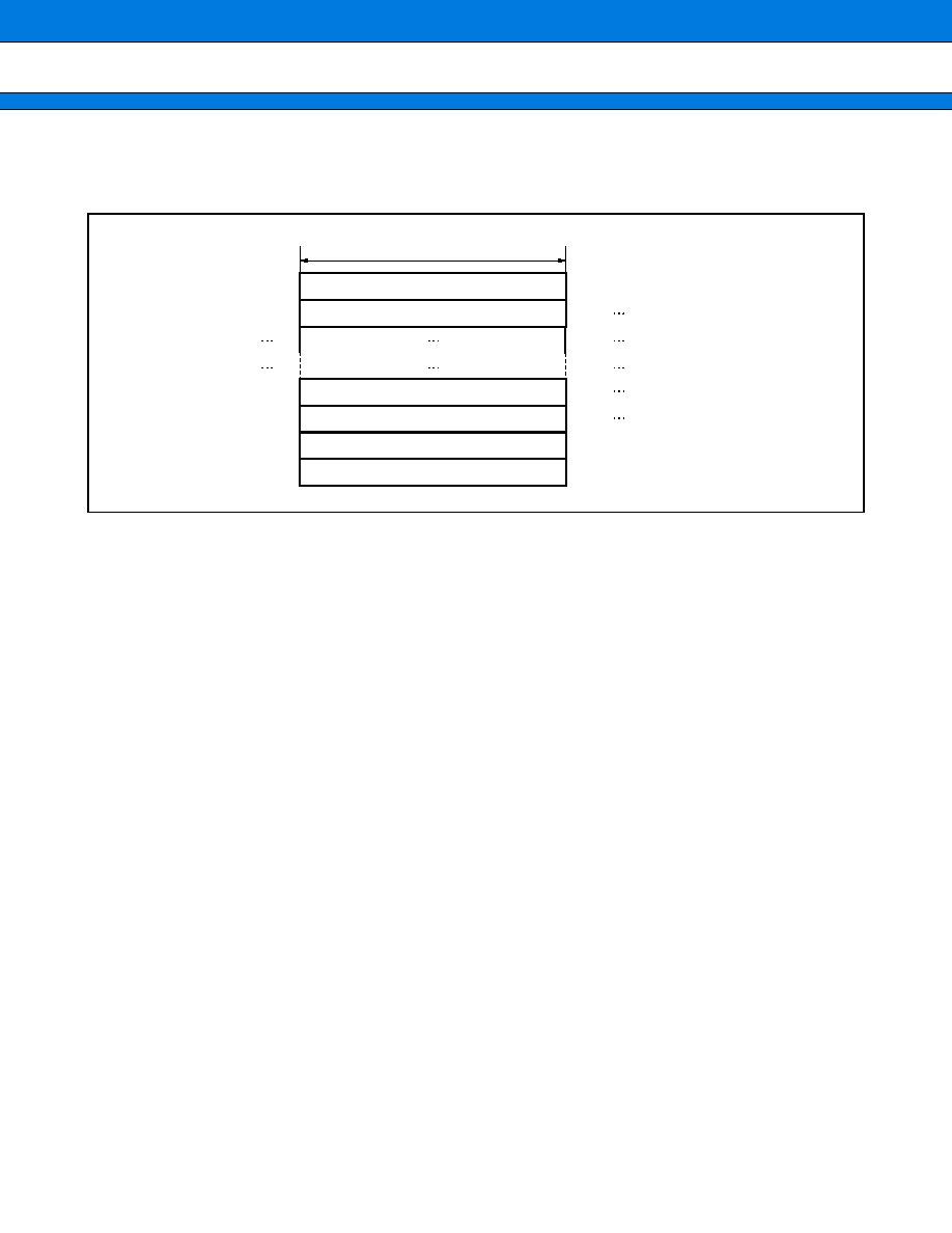
CPU
1.
Memory Space
The FR series has a 4Gbytes (2
32
bytes) logical address space and the CPU performs linear access.
∑
Memory map
The figure below shows the memory map for this device.
The various mode settings are determined by the mode vector fetch performed after INIT is negated.
(See "
s
MODE SETTINGS" for details of the mode settings.)
0000 0000
H
0000 0400
H
0001 0000
H
0002 0000
H
0003 F000
H
0004 0000
H
0005 C000
H
0006 0000
H
000E 0000
H
000F 0000
H
0010 0000
H
FFFF FFFF
H
0000 0000
H
0000 0400
H
0001 0000
H
0002 0000
H
0003 F000
H
0004 0000
H
0005 C000
H
0006 0000
H
000E 0000
H
000F 0000
H
0010 0000
H
FFFF FFFF
H
I/O
I/O
I/O
I/O
*1 : On the MB91V340, the prohibited access area and 112Kbytes RAM area are combined into a 128Kbytes
RAM area.
*2 : On the MB91V340, the 64Kbytes ROM area contains emulation RAM.
Internal
ROM/External bus mode
Access prohibited
Direct
addressing area
See "
s
I/O MAP"
External area
Internal RAM
4 Kbytes
External area
Access
prohibited*
1
Internal RAM
112 Kbytes*
1
External
ROM/External bus mode
Access prohibited
External area
External area
Access prohibited
Access prohibited
Internal ROM
64 Kbytes*
2
Internal RAM
4 Kbytes
MB91340/MB91V340
28
2.
Registers
The FR series has two types of registers: application-specific registers in the CPU and general purpose registers
in memory.
∑
Dedicated registers
∑
PC (Program Counter)
The PC is the program counter and stores the address of the currently executing instruction.
∑
Table base register (TBR)
The TBR is the table base register and stores the top address of the vector table used by the EIT function.
Program counter (PC)
: 32-bit register. Stores the current instruction address.
Program status (PS)
: 32-bit register. Contains the register pointer and condition code.
Table base register (TBR)
: Stores the top address of the vector table used by the EIT (exception/interrupt/
trap) function.
Return pointer (RP)
: Stores the subroutine return address.
System stack pointer (SSP) : Points to the system stack area.
User stack pointer (USP)
: Points to the user stack area.
Multiplication and division
result register (MDH/MDL)
: 32-bit registers used for multiplication and division.
PC
PS
TBR
RP
SSP
USP
MDH
MDL
XXXX XXXX
H
XXXX XXXX
H
XXXX XXXX
H
XXXX XXXX
H
XXXX XXXX
H
0000 0000
H
000F FC00
H
32 bit
Program counter
Program status
Table base register
Return pointer
System stack pointer
User stack pointer
Multiplication and division
result register
Initial value
PC
31
0
PC
TBR
31
0
TBR

MB91340/MB91V340
29
∑
Return pointer (RP)
The RP is the return pointer and stores the subroutine return address.
∑
System stack pointer (SSP)
The SSP is the system stack pointer and functions as R15 when the S flag is "0".
∑
User stack pointer (USP)
The USP is the user stack pointer and functions as R15 when the S flag is "1".
∑
Multiplication and division result register (MDH/MDL)
MDH/MDL : 32-bit registers used for multiplication and division.
MDH : Remainder
MDL : Quotient
RP
31
0
RP
SSP
31
0
SSP
USP
31
0
USP
Multiplication and division result register
31
0
MDH
MDL
MB91340/MB91V340
30
∑
Program status (PS)
This register holds the program status and is divided into the ILM, SCR, and CCR.
∑
Condition code register (CCR)
∑
System condition code register (SCR)
∑
Interrupt level mask register(ILM)
S flag
: Specifies which stack pointer to use as R15.
I flag
: Enables or disables user interrupt requests.
N flag
: Indicates the sign when an operation result is represented as a 2's complement integer.
Z flag
: Indicates whether an operation result is zero.
V flag
: Indicates whether an overflow occurred for an operation result when the operation operand is
represented as a 2's complement integer.
C flag
: Indicates whether an operation resulted in a borrow or a carry from the most significant bit.
D1, D0 flags
: Stores intermediate data for stepwise multiplication operations.
T flags
: A flag specifying whether the step trace trap function is enabled or not.
ILM4 to ILM0 : his register stores the interrupt level mask value. The value in the ILM register is used as the
level mask. Only interrupt requests to the CPU that have an interrupt level that is higher than
the level specified in ILM are accepted.
20
19
18
17
16
Initial Value
ILM4
ILM3
ILM2
ILM1
ILM0
Interrupt Level
01111
B
0
0
0
0
0
0
High
∑
∑
∑
∑
∑
∑
0
1
0
0
0
15
(Medium)
∑
∑
∑
∑
∑
∑
1
1
1
1
1
31
Low
ILM
Bit position
PS
31
20
16
ILM
SCR
CCR
10
7
8
0
Initial Value
- - 00XXXX
B
CCR
7
6
5
4
3
2
1
0
S
I
N
Z
V
C
Initial Value
XX0
B
SCR
10
9
8
D1
D0
T
MB91340/MB91V340
31
s
GENERAL PURPOSE REGISTERS
General purpose registers R0 to R15 are used by the CPU. The registers are used as the accumulator and
memory access pointers for CPU operations.
The following three registers are treated as having special meanings to enhance the operation of some instruc-
tions.
R13 : Virtual accumulator (AC)
R14 : Frame pointer (FP)
R15 : Stack pointer (SP)
The values of R0 to R14 after a reset are undefined. R15 is initialized to 0000 0000
H
(SSP value) .
R0
R1
R12
R13
R14
R15
AC (Accumulator)
FP (Frame Pointer)
SP (Stack Pointer)
XXXX XXXX
H
XXXX XXXX
H
0000 0000
H
Initial Value
32-bit
MB91340/MB91V340
32
s
MODE SETTINGS
In the FR series, the mode is set by the mode pins (MD2, 1, 0) and mode register (MODR).
1.
Pins
The MD2, MD1, and MD0 pins specify how the mode vector fetch is performed.
Values other than those listed in the table are prohibited.
2.
Register
∑ Mode register (MODR) and setting mode
The data written to the mode register by the mode vector fetch operation is called the mode data.
After the data is set to the mode register (MODR), the device operates with the operating mode specified by this
data.
The mode register is set by all types of reset. The register cannot be written to by user programs.
Note:
The address used by the mode register (0000 07FF
H
) was unused by previous FR series devices.
The register can be modified in emulator mode. In this case, use an 8-bit data transfer instruction. No data is
written by 16 or 32-bit transfer instructions.
<Register details>
ROMA : Specifies whether the internal Fbus RAM and Fbus ROM areas are enabled.
Mode Pins
Mode name
Reset vector access
area
Remarks
MD2
MD1
MD0
0
0
0
Internal ROM vector mode
Internal
0
0
1
External ROM vector mode
External
The bus width is specified by the
mode register.
ROMA
Function
Remarks
0
External ROM mode The internal Fbus area (4 0000
H
to 10 0000
H
) becomes an external area.
1
Internal ROM mode
The internal 112Kbytes of Fbus RAM (128Kbytes on the MB91V340) and
64Kbytes Fbus ROM are enabled.
bit 7 to 3 : Always set "00000
B
".
MODR
Initial Value
Access
XXXXXXXX
B
W
W
: Write-only
X
: Undefined
7
6
5
4
3
2
1
0
0
0
0
0
0
ROMA
WTH1
WTH0
Operation mode setting bits
MB91340/MB91V340
33
WTH1, WTH0 (Bus width setting bits) :
This sets the bus width in external bus mode. In external bus mode, the values of bits DBW1 and DBW0 in ACR0
(CS0 area) are set in these bits.
WTH1
WTH0
Function
Remarks
0
0
8-bit bus width
External bus mode
0
1
16-bit bus width
External bus mode
1
0
32-bit bus width
External bus mode
(only available on the MB91V340)
1
1
Single chip mode
Prohibited setting on this device.
MB91340/MB91V340
34
s
s
s
s
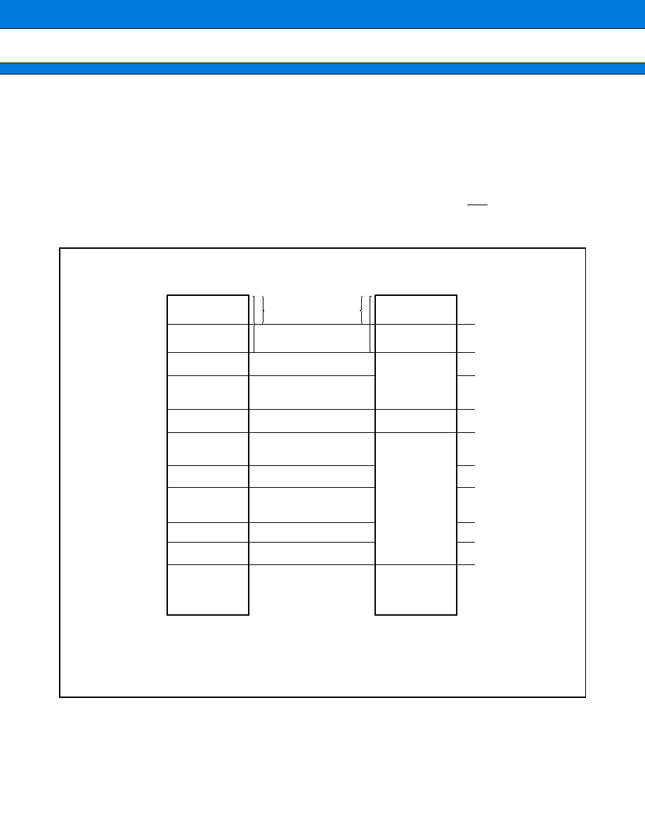
I/O MAP
This shows the location of the various peripheral resource registers in the memory space.
[How to read the table]
Note : Initial values of register bits are represented as follows :
(Continued)
"1" : Initial value"1"
"0" : Initial value"0"
"X" : Initial value"X"
"-"
: No physical register at this location
address
register
block
+
+
+
+
0
+
+
+
+
1
+
+
+
+
2
+
+
+
+
3
000000
H
PDR0 [R/W] B
*1
XXXXXXXX
PDR1 [R/W] B
*1
XXXXXXXX
PDR2 [R/W] B
XXXXXXXX
T-unit
Port Data
Register
000004
H
PDR6 [R/W] B
XXXXXXXX
000008
H
PDR8 [R/W] B
*2
-
-
XXXXXX
PDR9 [R/W] B
XXXXXXX-
PDRA [R/W] B
XXXXXXXX
PDRB [R/W] B
XXXXXXXX
00000C
H
PDRC [R/W] B
-
-
-
-
-
XXX
000010
H
PDRH [R/W] B
-
-
-
-
-
XXX
PDRI [R/W] B
-
-
XXXXXX
PDRJ [R/W] B
XXXXXXXX
R-bus
Port Data
Register
000014
H
PDRK [R/W] B
XXXXXXXX
PDRL [R/W] B
-
XXXXXXX
PDRM [R/W] B
-
-
-
-
XXXX
PDRN [R/W] B
XXXXXXXX
000018
H
PDRO [R/W] B
XXXXXXXX
PDRP [R/W] B
XXXXXXXX
00001C
H
address
register
block
+
+
+
+
0
+
+
+
+
1
+
+
+
+
2
+
+
+
+
3
000000
H
PDR0 [R/W] B
XXXXXXXX
PDR1 [R/W] B
XXXXXXXX
PDR2 [R/W] B
XXXXXXXX
PDR3 [R/W] B
XXXXXXXX
T-unit
Port Data Register
Read/write attribute, Access type
(B : Byte, H : Half Word, W : Word)
Register name (Address of column 1 register is 4n, address of column
2 register is 4n+2, etc.)
Location of left-most register (When using word access,
the register in column 1 is in the MSB side of the data.)
Initial value after a reset
MB91340/MB91V340
35
(Continued)
address
register
block
+
+
+
+
0
+
+
+
+
1
+
+
+
+
2
+
+
+
+
3
000020
H
to
00003C
H
Reserved
000040
H
EIRR [R/W] B, H, W
00000000
ENIR [R/W] B, H, W
00000000
ELVR [R/W] B, H, W
00000000
Ext int
000044
H
DICR [R/W] B, H, W
-
-
-
-
-
-
-
0
HRCL [R/W] B, H, W
0
-
-
11111
DLYI/I-unit
000048
H
TMRLR0 [W] H, W
XXXXXXXX XXXXXXXX
TMR0 [R] H, W
XXXXXXXX XXXXXXXX
Reload
Timer 0
00004C
H
TMCSR0 [R/W] B, H, W
-
-
-
-
0000 00000000
000050
H
TMRLR1 [W] H, W
XXXXXXXX XXXXXXXX
TMR1 [R] H, W
XXXXXXXX XXXXXXXX
Reload
Timer 1
000054
H
TMCSR1 [R/W] B, H, W
-
-
-
-
0000 00000000
000058
H
TMRLR2 [W] H, W
XXXXXXXX XXXXXXXX
TMR2 [R] H, W
XXXXXXXX XXXXXXXX
Reload
Timer 2
00005C
H
TMCSR2 [R/W] B, H, W
-
-
-
-
0000 00000000
000060
H
SSR0 [R/W] B, H, W
00001000
SIDR0 [R/W] B, H, W
XXXXXXXX
SCR0 [R/W] B, H, W
00000100
SMR0 [R/W] B, H, W
00
-
-
0
-
0
-
UART0
000064
H
UTIM0 [R] H (UTIMR0 [W] H)
00000000 00000000
DRCL0 [W] B
-
-
-
-
-
-
-
-
UTIMC0 [R/W] B
0
-
-
00001
U-TIMER
0
000068
H
SSR1 [R/W] B, H, W
00001000
SIDR1 [R/W] B, H, W
XXXXXXXX
SCR1 [R/W] B, H, W
00000100
SMR1 [R/W] B, H, W
00
-
-
0
-
0
-
UART1
00006C
H
UTIM1 [R] H (UTIMR1 [W] H )
00000000 00000000
DRCL1 [W] B
-
-
-
-
-
-
-
-
UTIMC1 [R/W] B
0
-
-
00001
U-TIMER
1
000070
H
SSR2 [R/W] B, H, W
00001000
SIDR2 [R/W] B, H, W
XXXXXXXX
SCR2 [R/W] B, H, W
00000100
SMR2 [R/W] B, H, W
00
-
-
0
-
0
-
UART2
000074
H
UTIM2 [R] H (UTIMR2 [W] H )
00000000 00000000
DRCL2 [W] B
-
-
-
-
-
-
-
-
UTIMC2 [R/W] B
0
-
-
00001
U-TIMER
2
000078
H
ADCR [R] B, H, W
000000XX XXXXXXXX
ADCS [R/W] B, H, W
00000000 00000000
A/D
Converter
Sequential
Compara-
tor
00007C
H
ADCR0 [R] B, H, W
XXXXXXXX
ADCR1 [R] B, H, W
XXXXXXXX
ADCR2 [R] B, H, W
XXXXXXXX
ADCR3 [R] B, H, W
XXXXXXXX
000080
H
ADCR4 [R] B, H, W
XXXXXXXX
ADCR5 [R] B, H, W
XXXXXXXX
ADCR6 [R] B, H, W
XXXXXXXX
ADCR7 [R] B, H, W
XXXXXXXX
000084
H
DACR2 [R/W] B, H, W
-
-
-
-
-
-
-
0
DACR1 [R/W] B, H, W
-
-
-
-
-
-
-
0
DACR0 [R/W] B, H, W
-
-
-
-
-
-
-
0
D/A
Converter
000088
H
DADR2 [R/W] B, H, W
XXXXXXXX
DADR1 [R/W] B, H, W
XXXXXXXX
DADR0 [R/W] B, H, W
XXXXXXXX
MB91340/MB91V340
36
(Continued)
address
register
block
+
+
+
+
0
+
+
+
+
1
+
+
+
+
2
+
+
+
+
3
00008C
H
WCR [R/W] B, H, W
00111111
APR [R/W] B, H, W
-
0000000
WDR1 [R/W] B, H, W
XXXXXXXX
WDR0 [R/W] B, H, W
XXXXXXXX
D/A DATA
Transmitter
000090
H
VERR [R] B, H, W
-
-
-
-
XXXX
Version
Register
000094
H
IBCR [R/W] B, H, W
00000000
IBSR [R] B, H, W
00000000
ITBA [R/W] B, H, W
-
-
-
-
-
-
00 00000000
I
2
C
interface
000098
H
ITMK [R/W] B, H, W
00
-
-
-
-
11 11111111
ISMK [R/W] B, H, W
01111111
ISBA [R/W] B, H, W
-
0000000
00009C
H
IDAR [R/W] B, H, W
00000000
ICCR [R/W] B, H, W
0-011111
IDBL [R/W] B, H, W
-
-
-
-
-
-
-
0
0000A0
H
Reserved
0000A4
H
0000A8
H
TMRLR3 [W] H, W
XXXXXXXX XXXXXXXX
TMR3 [R] H, W
XXXXXXXX XXXXXXXX
Reload
Timer 3
0000AC
H
TMCSR3 [R/W] B, H, W
-
-
-
-
0000 00000000
0000B0
H
RCR1 [W] B, H, W
00000000
RCR0 [W] B, H, W
00000000
UDCR1 [R] B, H, W
00000000
UDCR0 [R] B, H, W
00000000
8/16 Bit
U/D
Counter0, 1
0000B4
H
CCRH0 [R/W] B, H, W
00001000
CCRL0 [R/W] B, H, W
00001000
CSR0 [R/W] B, H, W
00000000
0000B8
H
CCRH1 [R/W] B, H, W
00001000
CCRL1 [R/W] B, H, W
00001000
CSR1 [R/W] B, H, W
00000000
0000BC
H
RCR3 [W] B, H, W
00000000
RCR2 [W] B, H, W
00000000
UDCR3 [R] B, H, W
00000000
UDCR2 [R] B, H, W
00000000
8/16 Bit
U/D
Counter2, 3
0000C0
H
CCRH2 [R/W] B, H, W
00001000
CCRL2 [R/W] B, H, W
00001000
CSR2 [R/W] B, H, W
00000000
0000C4
H
CCRH3 [R/W] B, H, W
00001000
CCRL3 [R/W] B, H, W
00001000
CSR3 [R/W] B, H, W
00000000
0000C8
H
Reserved
0000CC
H
0000D0
H
CCR [R/W] B, H, W
00001000
COMPR [R/W] B, H, W
00001000
CSR [R/W] B, H, W
00000000
UCR [R/W] B, H, W
00000000
8 Bit UP
Counter
0000D4
H
TCDT [R/W] H, W
00000000 00000000
TCCS [R/W] B, H, W
00000000
16 bit Free
run Timer
0000D8
H
IPCP1 [R] H, W
XXXXXXXX XXXXXXXX
IPCP0 [R] H, W
XXXXXXXX XXXXXXXX
16 bit ICU
0000DC
H
IPCP3 [R] H, W
XXXXXXXX XXXXXXXX
IPCP2 [R] H, W
XXXXXXXX XXXXXXXX
0000E0
H
ICS23 [R/W] B, H, W
00000000
ICS01 [R/W] B, H, W
00000000
MB91340/MB91V340
37
(Continued)
address
register
block
+
+
+
+
0
+
+
+
+
1
+
+
+
+
2
+
+
+
+
3
0000E4
H
OCCP1 [R/W] H, W
XXXXXXXX XXXXXXXX
OCCP0 [R/W] H, W
XXXXXXXX XXXXXXXX
16 bit OCU
0000E8
H
OCCP3 [R/W] H, W
XXXXXXXX XXXXXXXX
OCCP2 [R/W] H, W
XXXXXXXX XXXXXXXX
0000EC
H
OCCP5 [R/W] H, W
XXXXXXXX XXXXXXXX
OCCP4 [R/W] H, W
XXXXXXXX XXXXXXXX
0000F0
H
OCCP7 [R/W] H, W
XXXXXXXX XXXXXXXX
OCCP6 [R/W] H, W
XXXXXXXX XXXXXXXX
0000F4
H
OCS23 [R/W] B, H, W
1110110 00001100
OCS01 [R/W] B, H, W
1110110 00001100
0000F8
H
OCS67 [R/W] B, H, W
1110110 00001100
OCS45 [R/W] B, H, W
1110110 00001100
0000FC
H
to
0001FC
H
Reserved
000200
H
DMACA0 [R/W] B, H, W*
3
00000000 0000XXXX XXXXXXXX XXXXXXXX
DMAC
000204
H
DMACB0 [R/W] B, H, W
00000000 00000000 XXXXXXXX XXXXXXXX
000208
H
DMACA1 [R/W] B, H, W*
3
00000000 0000XXXX XXXXXXXX XXXXXXXX
00020C
H
DMACB1 [R/W] B, H, W
00000000 00000000 XXXXXXXX XXXXXXXX
000210
H
DMACA2 [R/W] B, H, W*
3
00000000 0000XXXX XXXXXXXX XXXXXXXX
000214
H
DMACB2 [R/W] B, H, W
00000000 00000000 XXXXXXXX XXXXXXXX
000218
H
DMACA3 [R/W] B, H, W*
3
00000000 0000XXXX XXXXXXXX XXXXXXXX
00021C
H
DMACB3 [R/W] B, H, W
00000000 00000000 XXXXXXXX XXXXXXXX
000220
H
DMACA4 [R/W] B, H, W*
3
00000000 0000XXXX XXXXXXXX XXXXXXXX
000224
H
DMACB4 [R/W] B, H, W
00000000 00000000 XXXXXXXX XXXXXXXX
000228
H
00022C
H
to
00023C
H
Reserved
000240
H
DMACR [R/W] B
0XX00000 XXXXXXXX XXXXXXXX XXXXXXXX
DMAC
MB91340/MB91V340
38
(Continued)
address
register
block
+
+
+
+
0
+
+
+
+
1
+
+
+
+
2
+
+
+
+
3
000244
H
to
000300
H
Reserved
000304
H
ISIZE [R/W] B, H, W
-
-
-
-
-
-
11
I-Cache
(MB91V340
only)
000308
H
to
0003E0
H
Reserved
0003E4
H
ICHCR [R/W] B, H,
W
0
-
000000
I-Cache
(MB91V340
only)
0003E8
H
Reserved
0003EC
H
0003F0
H
BSD0 [W]
XXXXXXXX XXXXXXXX XXXXXXXX XXXXXXXX
Bit Search
Module
0003F4
H
BSD1 [R/W]
XXXXXXXX XXXXXXXX XXXXXXXX XXXXXXXX
0003F8
H
BSDC [W]
XXXXXXXX XXXXXXXX XXXXXXXX XXXXXXXX
0003FC
H
BSRR [R]
XXXXXXXX XXXXXXXX XXXXXXXX XXXXXXXX
000400
H
DDRH [R/W] B
-
-
-
-
-
000
DDRI [R/W] B
-
-
000000
DDRJ [R/W] B
00000000
R-bus
Data
Direction
Register
000404
H
DDRK [R/W] B
00000000
DDRL [R/W] B
-
0000000
DDRM [R/W] B
-
-
-
-
0000
DDRN [R/W] B
00000000
000408
H
DDRO [R/W] B
00000000
DDRP [R/W] B
00000000
00040C
H
000410
H
PFRH [R/W] B
-
-
-
-
-
00
-
PFRI [R/W] B
-
-
00
-
00
-
R-bus
Port Function
Register
000414
H
PFRK [R/W] B
0000
-
-
-
-
PFRL [R/W] B
00-
-
-
000
000418
H
PFRO [R/W]
00000000
00041C
H
Reserved
000420
H
PCRH [R/W] B
-
-
-
-
-
000
PCRI [R/W] B
-
-
000000
PCRJ [R/W] B
00000000
R-bus
Pull-up
Control
Register
MB91340/MB91V340
39
(Continued)
address
register
block
+
+
+
+
0
+
+
+
+
1
+
+
+
+
2
+
+
+
+
3
000424
H
PCRK [R/W] B
00000000
PCRL [R/W] B
-
0
0
0
0
000
PCRM [R/W] B
-
-
-
-000
PCRN [R/W] B
00000000
R-bus
Pull-up
Control
Register
000428
H
PCRO [R/W] B
00000000
PCRP [R/W] B
00000000
00042C
H
to
00043C
H
Reserved
000440
H
ICR00 [R/W] B, H, W
-
-
-
11111
ICR01 [R/W] B, H, W
-
-
-
11111
ICR02 [R/W] B, H, W
-
-
-
11111
ICR03 [R/W] B, H, W
-
-
-
11111
Interrupt
Control
unit
000444
H
ICR04 [R/W] B, H, W
-
-
-
11111
ICR05 [R/W] B, H, W
-
-
-
11111
ICR06 [R/W] B, H, W
-
-
-
11111
ICR07 [R/W] B, H, W
-
-
-
11111
000448
H
ICR08 [R/W] B, H, W
-
-
-
11111
ICR09 [R/W] B, H, W
-
-
-
11111
ICR10 [R/W] B, H, W
-
-
-
11111
ICR11 [R/W] B, H, W
-
-
-
11111
00044C
H
ICR12 [R/W] B, H, W
-
-
-
11111
ICR13 [R/W] B, H, W
-
-
-
11111
ICR14 [R/W] B, H, W
-
-
-
11111
ICR15 [R/W] B, H, W
-
-
-
11111
000450
H
ICR16 [R/W] B, H, W
-
-
-
11111
ICR17 [R/W] B, H, W
-
-
-
11111
ICR18 [R/W] B, H, W
-
-
-
11111
ICR19 [R/W] B, H, W
-
-
-
11111
000454
H
ICR20 [R/W] B, H, W
-
-
-
11111
ICR21 [R/W] B, H, W
-
-
-
11111
ICR22 [R/W] B, H, W
-
-
-
11111
ICR23 [R/W] B, H, W
-
-
-
11111
000458
H
ICR24 [R/W] B, H, W
-
-
-
11111
ICR25 [R/W] B, H, W
-
-
-
11111
ICR26 [R/W] B, H, W
-
-
-
11111
ICR27 [R/W] B, H, W
-
-
-
11111
00045C
H
ICR28 [R/W] B, H, W
-
-
-
11111
ICR29 [R/W] B, H, W
-
-
-
11111
ICR30 [R/W] B, H, W
-
-
-
11111
ICR31 [R/W] B, H, W
-
-
-
11111
000460
H
ICR32 [R/W] B, H, W
-
-
-
11111
ICR33 [R/W] B, H, W
-
-
-
11111
ICR34 [R/W] B, H, W
-
-
-
11111
ICR35 [R/W] B, H, W
-
-
-
11111
000464
H
ICR36 [R/W] B, H, W
-
-
-
11111
ICR37 [R/W] B, H, W
-
-
-
11111
ICR38 [R/W] B, H, W
-
-
-
11111
ICR39 [R/W] B, H, W
-
-
-
11111
000468
H
ICR40 [R/W] B, H, W
-
-
-
11111
ICR41 [R/W] B, H, W
-
-
-
11111
ICR42 [R/W] B, H, W
-
-
-
11111
ICR43 [R/W] B, H, W
-
-
-
11111
00046C
H
ICR44 [R/W] B, H, W
-
-
-
11111
ICR45 [R/W] B, H, W
-
-
-
11111
ICR46 [R/W] B, H, W
-
-
-
11111
ICR47 [R/W] B, H, W
-
-
-
11111
000470
H
to
00047C
H
000480
H
RSRR [R/W] B, H,
W
10000000
STCR [R/W] B, H, W
00110011
TBCR [R/W] B, H, W
00XXXX00
CTBR [W] B, H, W
XXXXXXXX
Clock
Control
unit
000484
H
CLKR [R/W] B, H, W
00000000
WPR [W] B, H, W
XXXXXXXX
DIVR0 [R/W] B, H, W
00000011
DIVR1 [R/W] B, H, W
00000000
000488
H
MB91340/MB91V340
40
(Continued)
address
register
block
+
+
+
+
0
+
+
+
+
1
+
+
+
+
2
+
+
+
+
3
00048C
H
to
0005FC
H
Reserved
000600
H
DDR0 [R/W] B*
1
00000000
DDR1 [R/W] B*
1
00000000
DDR2 [R/W] B
00000000
T-unit
Data Direc-
tion Register
000604
H
DDR6 [R/W] B
00000000
000608
H
DDR8 [R/W] B*
4
-
-
000000
DDR9 [R/W] B
00000000
DDRA [R/W] B
00000000
DDRB [R/W] B
00000000
00060C
H
DDRC [R/W] B
-
-
-
-
-
000
000610
H
T-unit
Port Func-
tion Register
000614
H
PFR6 [R/W] B
11111111
000618
H
PFR8 [R/W] B*
5
-
-
1
-
-
0
-
-
PFR9 [R/W] B
0
-
001001
PFRA [R/W] B
11111111
PFRB1 [R/W] B
00000000
00061C
H
PFRB2 [R/W] B
00
-
-
-
-
00
PFRC [R/W] B
-
-
-
00000
000620
H
PCR0 [R/W] B*
1
00000000
PCR1 [R/W] B*
1
00000000
PCR2 [R/W] B
00000000
T-unit
Pull-up Con-
trol Register
000624
H
PCR6 [R/W] B
00000000
000628
H
PCR8 [R/W] B*
4
-
-
000000
PCR9 [R/W] B
00000000
PCRA [R/W] B
00000000
PCRB [R/W] B
00000000
00062C
H
PCRC [R/W] B
-
-
-
-
-
000
000630
H
to
00063C
H
Reserved
000640
H
ASR0 [R/W] H, W
00000000 00000000
ACR0 [R/W] B, H, W
1111XX00 00000000
T-unit
000644
H
ASR1 [R/W] H, W
00000000 00000000
ACR1 [R/W] B, H, W
XXXXXXXX XXXXXXXX
000648
H
ASR2 [R/W] H, W
00000000 00000000
ACR2 [R/W] B, H, W
XXXXXXXX XXXXXXXX
00064C
H
ASR3 [R/W] H, W
00000000 00000000
ACR3 [R/W] B, H, W
XXXXXXXX XXXXXXXX
000650
H
ASR4 [R/W] H, W
00000000 00000000
ACR4 [R/W] B, H, W
XXXXXXXX XXXXXXXX
T-unit
000654
H
ASR5 [R/W] H, W
00000000 00000000
ACR5 [R/W] B, H, W
XXXXXXXX XXXXXXXX
MB91340/MB91V340
41
(Continued)
address
register
block
+
+
+
+
0
+
+
+
+
1
+
+
+
+
2
+
+
+
+
3
000658
H
ASR6 [R/W] H, W
00000000 00000000
ACR6 [R/W] B, H, W
XXXXXXXX XXXXXXXX
T
-
unit
00065C
H
ASR7 [R/W] H, W
00000000 00000000
ACR7 [R/W] B, H, W
XXXXXXXX XXXXXXXX
000660
H
AWR0 [R/W] B, H, W
01111111 11111111
AWR1 [R/W] B, H, W
XXXXXXXX XXXXXXXX
000664
H
AWR2 [R/W] B, H, W
XXXXXXXX XXXXXXXX
AWR3 [R/W] B, H, W
XXXXXXXX XXXXXXXX
000668
H
AWR4 [R/W] B, H, W
XXXXXXXX XXXXXXXX
AWR5 [R/W] B, H, W
XXXXXXXX XXXXXXXX
00066C
H
AWR6 [R/W] B, H, W
XXXXXXXX XXXXXXXX
AWR7 [R/W] B, H, W
XXXXXXXX XXXXXXXX
000670
H
000674
H
000678
H
IOWR0 [R/W] B, H, W
XXXXXXXX
IOWR1 [R/W] B, H, W
XXXXXXXX
IOWR2 [R/W] B, H, W
XXXXXXXX
00067C
H
000680
H
CSER [R/W] B, H, W
00000001
CheR [R/W]
B, H, W*
1
11111111
TCR [W] B, H, W
0000XXXX
000684
H
000684
H
to
0007F8
H
Reserved
0007FC
H
MODR [W]*
6
XXXXXXXX
000800
H
to
000AFC
H
Reserved
000B00
H
ESTS0 [R/W]
X0000000
ESTS1 [R/W]
XXXXXXXX
ESTS2 [R]
1XXXXXXX
DSU
(MB91V34
0
only )
000B04
H
ECTL0 [R/W]
0X000000
ECTL1 [R/W]
00000000
ECTL2 [W]
000X0000
ECTL3 [R/W]
00X00X11
000B08
H
ECNT0 [W]
XXXXXXXX
ECNT1 [W]
XXXXXXXX
EUSA [W]
XXX00000
EDTC [W]
0000XXXX
000B0C
H
EWPT [R]
00000000 00000000
000B10
H
EDTR0 [W]
XXXXXXXX XXXXXXXX
EDTR1 [W]
XXXXXXXX XXXXXXXX
MB91340/MB91V340
42
(Continued)
address
register
block
+
+
+
+
0
+
+
+
+
1
+
+
+
+
2
+
+
+
+
3
000B14
H
to
000B1C
H
DSU
(MB91V340
only )
000B20
H
EIA0 [W]
XXXXXXXX XXXXXXXX XXXXXXXX XXXXXXXX
000B24
H
EIA1 [W]
XXXXXXXX XXXXXXXX XXXXXXXX XXXXXXXX
000B28
H
EIA2 [W]
XXXXXXXX XXXXXXXX XXXXXXXX XXXXXXXX
000B2C
H
EIA3 [W]
XXXXXXXX XXXXXXXX XXXXXXXX XXXXXXXX
000B30
H
EIA4 [W]
XXXXXXXX XXXXXXXX XXXXXXXX XXXXXXXX
000B34
H
EIA5 [W]
XXXXXXXX XXXXXXXX XXXXXXXX XXXXXXXX
000B38
H
EIA6 [W]
XXXXXXXX XXXXXXXX XXXXXXXX XXXXXXXX
000B3C
H
EIA7 [W]
XXXXXXXX XXXXXXXX XXXXXXXX XXXXXXXX
000B40
H
EDTA [R/W]
XXXXXXXX XXXXXXXX XXXXXXXX XXXXXXXX
000B44
H
EDTM [R/W]
XXXXXXXX XXXXXXXX XXXXXXXX XXXXXXXX
000B48
H
EOA0 [W]
XXXXXXXX XXXXXXXX XXXXXXXX XXXXXXXX
000B4C
H
EOA1 [W]
XXXXXXXX XXXXXXXX XXXXXXXX XXXXXXXX
000B50
H
EPCR [R/W]
XXXXXXXX XXXXXXXX XXXXXXXX XXXXXXXX
000B54
H
EPSR [R/W]
XXXXXXXX XXXXXXXX XXXXXXXX XXXXXXXX
000B58
H
EIAM0 [W]
XXXXXXXX XXXXXXXX XXXXXXXX XXXXXXXX
000B5C
H
EIAM1 [W]
XXXXXXXX XXXXXXXX XXXXXXXX XXXXXXXX
000B60
H
EOAM0/EODM0 [W]
XXXXXXXX XXXXXXXX XXXXXXXX XXXXXXXX
000B64
H
EOAM1/EODM1 [W]
XXXXXXXX XXXXXXXX XXXXXXXX XXXXXXXX
000B68
H
EOD0 [W]
XXXXXXXX XXXXXXXX XXXXXXXX XXXXXXXX
MB91340/MB91V340
43
(Continued)
*1 : This register is only present on the MB91V340.
*2 : The Initial value of this register on the MB91V340 is [XXXXXXXX].
*3 : Byte access is not permitted for the lower 16 bits of DMAC0 to 4 (DTC[15:0])
*4: The default value of this register on the MB91V340 is [00000000].
*5: The default value of this register on the MB91V340 is [111
-
-
0
-
-].
*6 : This register is accessed through mode vector fetch; it cannot be accessed in normal mode.
address
register
block
+
+
+
+
0
+
+
+
+
1
+
+
+
+
2
+
+
+
+
3
000B6C
H
EOD1 [W]
XXXXXXXX XXXXXXXX XXXXXXXX XXXXXXXX
DSU
(
MB91V340
)
000B70
H
to
000FFC
H
Reserved
001000
H
DMASA0 [R/W] W
XXXXXXXX_XXXXXXXX_XXXXXXXX_XXXXXXXX
DMAC
001004
H
DMADA0 [R/W] W
XXXXXXXX_XXXXXXXX_XXXXXXXX_XXXXXXXX
001008
H
DMASA1 [R/W] W
XXXXXXXX_XXXXXXXX_XXXXXXXX_XXXXXXXX
00100C
H
DMADA1 [R/W] W
XXXXXXXX_XXXXXXXX_XXXXXXXX_XXXXXXXX
001010
H
DMASA2 [R/W] W
XXXXXXXX_XXXXXXXX_XXXXXXXX_XXXXXXXX
001014
H
DMADA2 [R/W] W
XXXXXXXX_XXXXXXXX_XXXXXXXX_XXXXXXXX
001018
H
DMASA3 [R/W] W
XXXXXXXX_XXXXXXXX_XXXXXXXX_XXXXXXXX
00101C
H
DMADA3 [R/W] W
XXXXXXXX_XXXXXXXX_XXXXXXXX_XXXXXXXX
001020
H
DMASA4 [R/W] W
XXXXXXXX_XXXXXXXX_XXXXXXXX_XXXXXXXX
001024
H
DMADA4 [R/W] W
XXXXXXXX_XXXXXXXX_XXXXXXXX_XXXXXXXX
001028
H
to
001FFC
H
Reserved
MB91340/MB91V340
44
s
INTERRUPT VECTORS
(Continued)
Interrupt
Interrupt No.
Interrupt
level
Offset
TBR default
address
RN
Number
Reset
#0
00
H
3FC
H
000FFFFC
H
Mode vector
#1
01
H
3F8
H
000FFFF8
H
System reserved
#2
02
H
3F4
H
000FFFF4
H
System reserved
#3
03
H
3F0
H
000FFFF0
H
System reserved
#4
04
H
3EC
H
000FFFEC
H
System reserved
#5
05
H
3E8
H
000FFFE8
H
System reserved
#6
06
H
3E4
H
000FFFE4
H
Coprocessor absent trap
#7
07
H
3E0
H
000FFFE0
H
Coprocessor error trap
#8
08
H
3DC
H
000FFFDC
H
INTE instruction
#9
09
H
3D8
H
000FFFD8
H
Instruction break exception
#10
0A
H
3D4
H
000FFFD4
H
Operand break trap
#11
0B
H
3D0
H
000FFFD0
H
Step trace trap
#12
0C
H
3CC
H
000FFFCC
H
NMI request (tool)
#13
0D
H
3C8
H
000FFFC8
H
Undefined instruction exception
#14
0E
H
3C4
H
000FFFC4
H
NMI request
#15
0F
H
15 (F
H
)
fixed
3C0
H
000FFFC0
H
External interrupt 0
#16
10
H
ICR00
3BC
H
000FFFBC
H
6
External interrupt 1
#17
11
H
ICR01
3B8
H
000FFFB8
H
7
External interrupt 2
#18
12
H
ICR02
3B4
H
000FFFB4
H
11
External interrupt 3
#19
13
H
ICR03
3B0
H
000FFFB0
H
12
External interrupt 4
#20
14
H
ICR04
3AC
H
000FFFAC
H
External interrupt 5
#21
15
H
ICR05
3A8
H
000FFFA8
H
External interrupt 6
#22
16
H
ICR06
3A4
H
000FFFA4
H
External interrupt 7
#23
17
H
ICR07
3A0
H
000FFFA0
H
Reload timer 0
#24
18
H
ICR08
39C
H
000FFF9C
H
8
Reload timer 1
#25
19
H
ICR09
398
H
000FFF98
H
9
Reload timer 2
#26
1A
H
ICR10
394
H
000FFF94
H
10
UART0 (RX completed)
#27
1B
H
ICR11
390
H
000FFF90
H
0
UART1 (RX completed)
#28
1C
H
ICR12
38C
H
000FFF8C
H
1
UART2 (RX completed)
#29
1D
H
ICR13
388
H
000FFF88
H
2
UART0 (TX completed)
#30
1E
H
ICR14
384
H
000FFF84
H
3
UART1 (TX completed)
#31
1F
H
ICR15
380
H
000FFF80
H
4
UART2 (TX completed)
#32
20
H
ICR16
37C
H
000FFF7C
H
5
MB91340/MB91V340
45
(Continued)
Interrupt
Interrupt No.
Interrupt
level
Offset
TBR default
address
RN
Number
DMAC0 (end, error)
#33
21
H
ICR17
378
H
000FFF78
H
DMAC1 (end, error)
#34
22
H
ICR18
374
H
000FFF74
H
DMAC2 (end, error)
#35
23
H
ICR19
370
H
000FFF70
H
DMAC3 (end, error)
#36
24
H
ICR20
36C
H
000FFF6C
H
DMAC4 (end, error)
#37
25
H
ICR21
368
H
000FFF68
H
A/D
#38
26
H
ICR22
364
H
000FFF64
H
15
I
2
C
#39
27
H
ICR23
360
H
000FFF60
H
U/D counter 0
#40
28
H
ICR24
35C
H
000FFF5C
H
U/D counter 1
#41
29
H
ICR25
358
H
000FFF58
H
U/D counter 2
#42
2A
H
ICR26
354
H
000FFF54
H
U/D counter 3
#43
2B
H
ICR27
350
H
000FFF50
H
U-TIMER0
#44
2C
H
ICR28
34C
H
000FFF4C
H
U-TIMER1
#45
2D
H
ICR29
348
H
000FFF48
H
U-TIMER2
#46
2E
H
ICR30
344
H
000FFF44
H
Time base timer overflow
#47
2F
H
ICR31
340
H
000FFF40
H
Reload timer 3
#48
30
H
ICR32
33C
H
000FFF3C
H
13
UP counter
#49
31
H
ICR33
338
H
000FFF38
H
14
System reserved
#50
32
H
ICR34
334
H
000FFF34
H
System reserved
#51
33
H
ICR35
330
H
000FFF30
H
16 bit freerun timer
#52
34
H
ICR36
32C
H
000FFF2C
H
ICU0 (capture)
#53
35
H
ICR37
328
H
000FFF28
H
ICU1 (capture)
#54
36
H
ICR38
324
H
000FFF24
H
ICU2 (capture)
#55
37
H
ICR39
320
H
000FFF20
H
ICU3 (capture)
#56
38
H
ICR40
31C
H
000FFF1C
H
OCU0 (match)
#57
39
H
ICR41
318
H
000FFF18
H
OCU1 (match)
#58
3A
H
ICR42
314
H
000FFF14
H
OCU2 (match)
#59
3B
H
ICR43
310
H
000FFF10
H
OCU3 (match)
#60
3C
H
ICR44
30C
H
000FFF0C
H
OCU4/5 (match)
#61
3D
H
ICR45
308
H
000FFF08
H
OCU6/7 (match)
#62
3E
H
ICR46
304
H
000FFF04
H
Delay interrupt bit
#63
3F
H
ICR47
300
H
000FFF00
H
System reserved (Used by REALOS)
#64
40
H
2FC
H
000FFEFC
H
System reserved (Used by REALOS)
#65
41
H
2F8
H
000FFEF8
H
System reserved
#66
42
H
2F4
H
000FFEF4
H
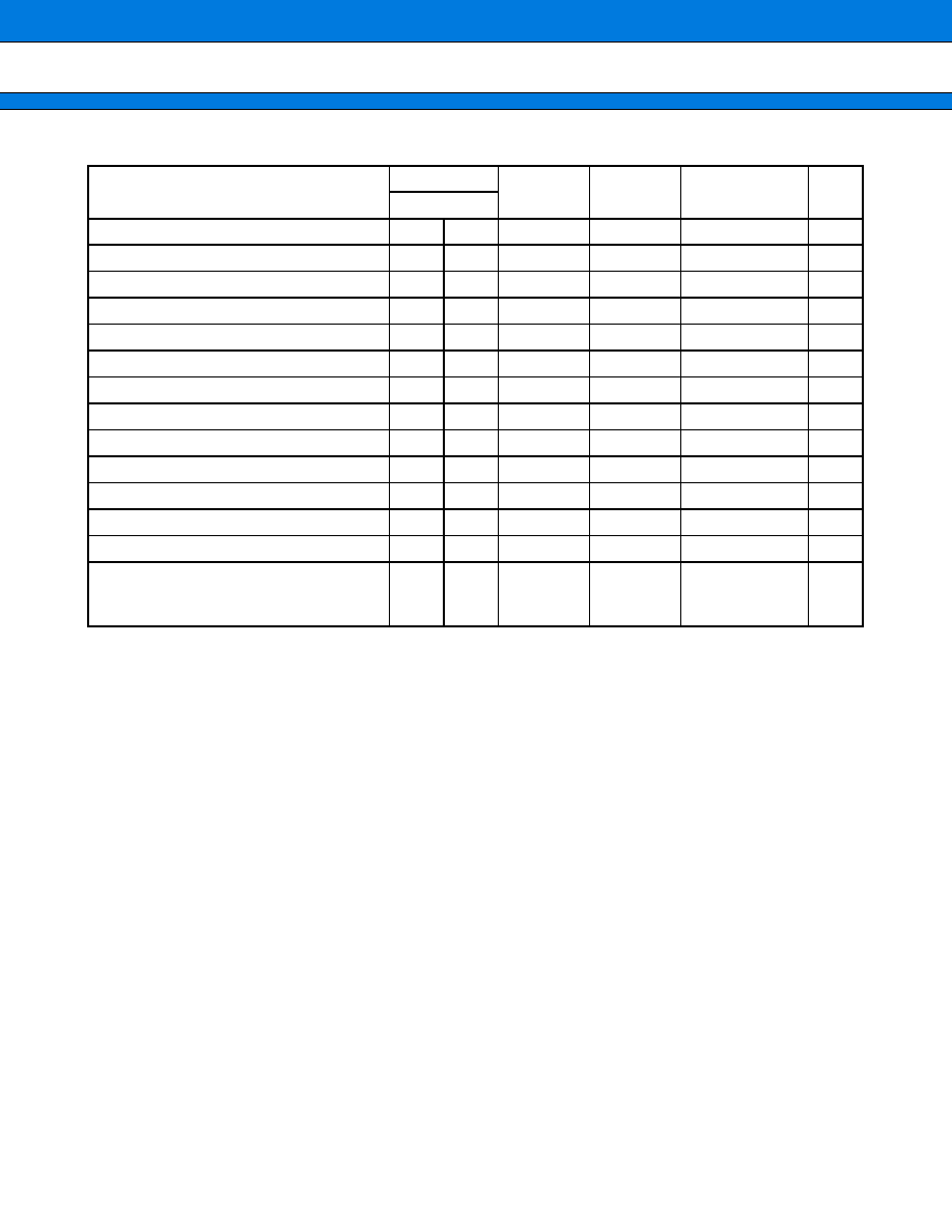
MB91340/MB91V340
46
(Continued)
Interrupt
Interrupt No.
Interrupt
level
Offset
TBR default
address
RN
Number
System reserved
#67
43
H
2F0
H
000FFEF0
H
System reserved
#68
44
H
2EC
H
000FFEEC
H
System reserved
#69
45
H
2E8
H
000FFEE8
H
System reserved
#70
46
H
2E4
H
000FFEE4
H
System reserved
#71
47
H
2E0
H
000FFEE0
H
System reserved
#72
48
H
2DC
H
000FFEDC
H
System reserved
#73
49
H
2D8
H
000FFED8
H
System reserved
#74
4A
H
2D4
H
000FFED4
H
System reserved
#75
4B
H
2D0
H
000FFED0
H
System reserved
#76
4C
H
2CC
H
000FFECC
H
System reserved
#77
4D
H
2C8
H
000FFEC8
H
System reserved
#78
4E
H
2C4
H
000FFEC4
H
System reserved
#79
4F
H
2C0
H
000FFEC0
H
Used by INT instruction
#80
to
#255
50
H
to
FF
H
2BC
H
to
000
H
000FFEBC
H
to
000FFC00
H

MB91340/MB91V340
47
s
PERIPHERAL RESOURCES
This section describes the location of each peripheral resource register in the memory space.
1.
External Bus Interface Controller
The external bus interface controller controls the interface between the LSI's internal bus and external memory
and I/O devices.
∑
∑
∑
∑
External Bus Interface Controller Features
∑ Maximum output address width = 32-bit (4GB memory space)
∑ Various different types of external memory (8-bit, 16-bit, or 32-bit devices) can be directly connected and the
controller can support multiple devices with different access timings.
Asynchronous SRAM, asynchronous ROM/FLASH memory (supports multiple write strobe access or byte-
enable access)
Page mode ROM/FLASH memory (2, 4, or 8 page size)
Burst mode ROM/FLASH memory (MBM29BL160D/161D/162D or equivalent)
Address/data multiplexed bus (8-bit or 16-bit width only)
Synchronous memory (ASIC internal memory, etc.)
Note:
Synchronous SRAM cannot be directly connected.
∑ Memory can be divided into eight independent banks (chip select areas) with a separate chip select output
for each bank.
The size of each area can be set in 64Kbyte increments (the size of each chip select area can range from
64Kbyte to 2Gbyte)
Each area can be located anywhere in the physical address space (subject to boundary limitations based on
the area size)
∑ The following functions can be set independently for each chip select area :
Chip select area enable/disable (Access is not performed to disabled areas)
Access timing type settings to suit the type of memory used
Detailed access timing settings (wait cycles and similar settings for each access type)
Data bus width (8-bit, 16-bit, 32-bit)
Byte-ordering setting (big or little endian)
Note:
The CS0 area must be big endian.
Write-prohibit setting (read-only areas)
Enable or disable loading into internal cache
Enable or disable prefetch function
Maximum burst length setting (1, 2, 4, 8)
∑ Different detailed timing settings can be set for each timing type
Even for the same type, different settings can be used for each chip select area.
Up to 15 auto-wait cycles can be specified. (For asynchronous SRAM, ROM, Flash, and I/O areas)
The bus cycle can be extended by the external RDY input. (For asynchronous SRAM, ROM, Flash, and I/O
areas)
Fast access wait and page wait settings are supported (For burst/page mode ROM and Flash areas)
Idle cycles, recovery cycles, setup delays, and similar can be inserted.
∑ DMA supports fly-by transfer
Transfer between memory and I/O can be performed by a single access.
Memory wait cycles can be synchronized with the I/O wait period during fly-by transfer.
Hold times can be maintained by extending access to the data source only.
Separate idle and recovery cycle settings can be specified for use in fly-by transfer.
∑ Supports external bus arbitration using BRQ and BGRNT.
∑ Pins not used by the external interface can be set as general purpose I/O ports.
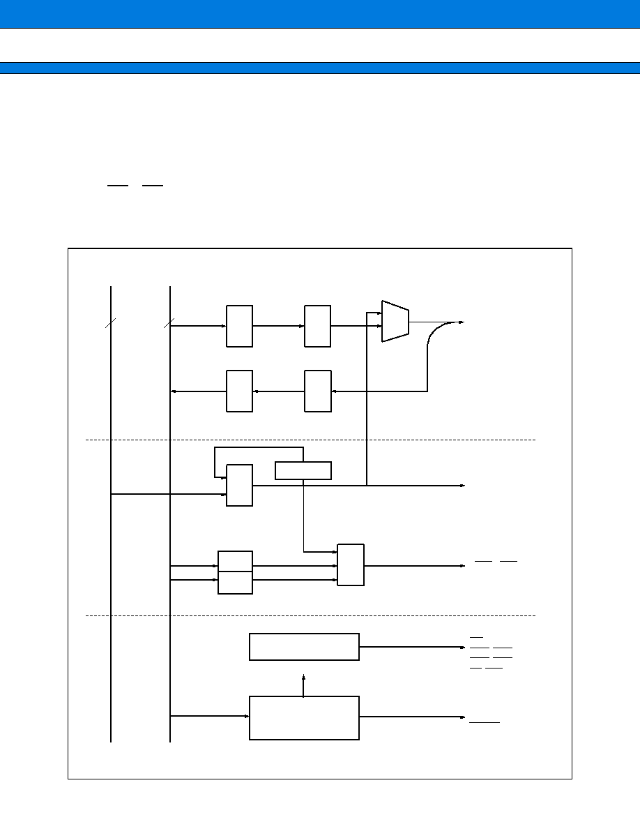
MB91340/MB91V340
48
∑
∑
∑
∑
Chip select areas
The external bus interface supports up to eight separate chip select area settings.
The address range for each area can be set anywhere in the 4Gbyte memory space in 64Kbyte increments.
The address settings for each area are set in ASR0 to ASR7 (Area Select Register) and ACR0 to ACR7 (Area
Configuration Register).
When bus access is performed to one of the areas specified in these registers, the corresponding chip select
signal (CS0 to CS7) is asserted (outputs "L") for the duration of the access cycle.
After a reset and until a value is written to ACR0, address range 00000000
H
to FFFFFFFF
H
is assigned to chip
select area 0.
∑
Block Diagram
MUX
CS0
CS7
RD
WR0, WR1
WR2, WR3
AS, BAA
BRQ
BGRNT
RDY
32
32
write buffer
read buffer
switch
switch
+
1 or
+
2
address buffer
ASR
ASZ
comparator
DATA BLOCK
ADDRESS BLOCK
resisters
&
control
External pin controller
All block control
Internal
address bus
Internal
data bus
External data bus
External address
bus
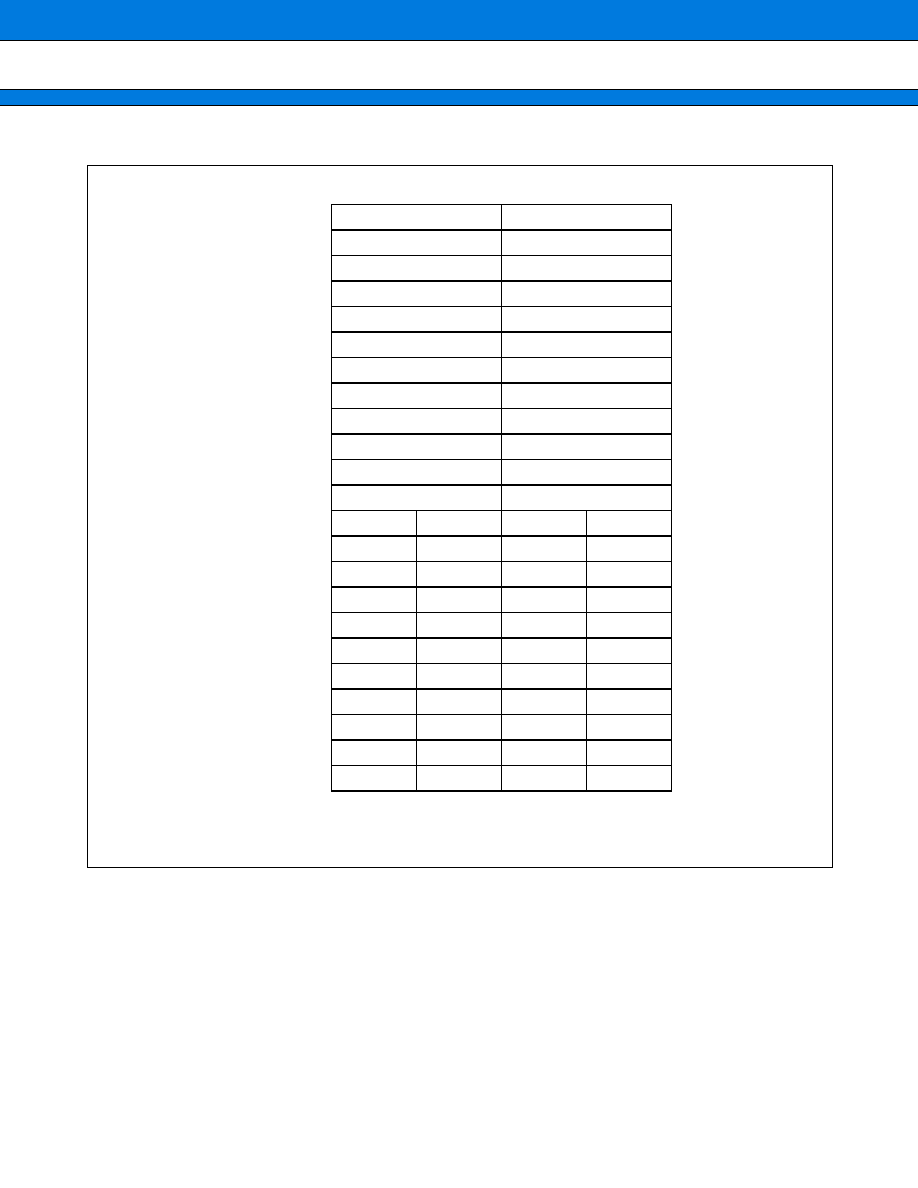
MB91340/MB91V340
49
∑
Register List
Reserved : Indicates a reserved register. When writing, always set to "0".
The MODR register cannot be accessed by the user program.
Address
31 24 23 16 15 08 07 00
00000640
H
ASR0
ACR0
00000644
H
ASR1
ACR1
00000648
H
ASR2
ACR2
0000064C
H
ASR3
ACR3
00000650
H
ASR4
ACR4
00000654
H
ASR5
ACR5
00000658
H
ASR6
ACR6
0000065C
H
ASR7
ACR7
00000660
H
AWR0
AWR1
00000664
H
AWR2
AWR3
00000668
H
AWR4
AWR5
0000066C
H
AWR6
AWR7
00000670
H
Reserved
Reserved
Reserved
Reserved
00000674
H
Reserved
Reserved
Reserved
Reserved
00000678
H
IOWR0
IOWR1
IOWR2
Reserved
0000067C
H
Reserved
Reserved
Reserved
Reserved
00000680
H
CSER
CHER
Reserved
Reserved
00000684
H
Reserved
Reserved
Reserved
Reserved
00000688
H
Reserved
Reserved
Reserved
Reserved
0000068C
H
Reserved
Reserved
Reserved
Reserved
000007F8
H
Reserved
Reserved
Reserved
Reserved
000007FC
H
Reserved
(MODR)
Reserved
Reserved
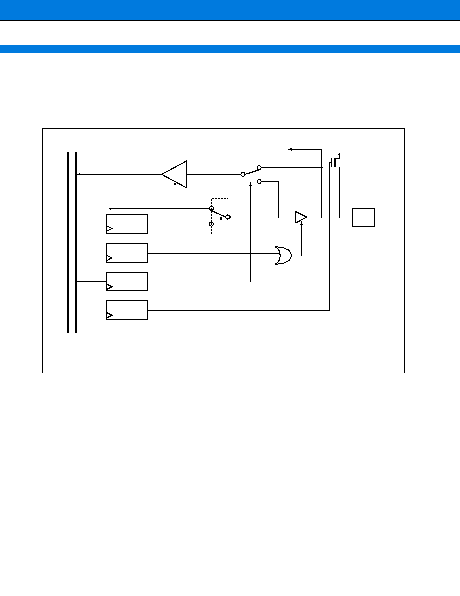
MB91340/MB91V340
50
2.
I/O Ports
MB91340/MB91V340 pins can be used as I/O ports when not set for use by the external bus interface or the
various peripheral I/O functions.
∑
I/O port (with pull-up resistor) block diagram
∑
I/O port registers
I/O ports with pull-up resistors have the following registers :
∑
PDR (Port Data Register)
∑
DDR (Data Direction Register)
∑
PFR (Port Function Register)
∑
PCR (Pull-up Control Register)
∑ When port is in input mode (PFR
=
"0" & DDR
=
"0")
PDR read : Reads the level of the corresponding external pin.
PDR write : PDRWrites the value to the PDR.
∑ When port is in output mode (PFR
=
"0" & DDR
=
"1")
PDR read : Reads the PDR value.
PDR write : Outputs the PDR value to the corresponding external pin.
∑ When port is in peripheral output mode (PFR
=
"1" & DDR
=
"X")
PDR : Reads the value of the corresponding peripheral output.
PDR write : Writes the value to the PDR.
Port Bus
0
1
1
0
Pin
PDR
PFR
DDR
PCR
DDR
PDR
PFR
PCR
: Data Direction Register
: Port Data Register
: Port Function Register
: Pull-up Control Register
Peripheral output
PDR read
Peripheral input
Pull-up resistor
(approx. 25 K
)
PCR
=
0 : No pull-up resistor
PCR
=
1 : Use pull-up resistor

MB91340/MB91V340
51
Notes :
∑
Use byte access to access ports.
∑
The external bus function has priority for port 0 to port A when these are used as external bus pins.
Accordingly, writing to the DDR has no effect on the pin input/output setting while the pins are operating
as external bus pins. The value set in the DDR becomes meaningful when the PFR register is modified
to set the pins as general purpose ports.
∑
In stop mode (HiZ = 0), the pull-up resistor control register setting is used.
∑
In stop mode (HiZ = 1), the pull-up resistor control register setting is ignored during hardware standby.
∑
Using pull-up resistors is prohibited when these pins are used as external bus pins. In this case, do not
write '1" to the corresponding bit in the pull-up control register (PCR).
MB91340/MB91V340
52
∑
Port Data Register (PDR)
(Continued)
PDR0
Initial value
Access
Address : 00000000
H
XXXXXXXX
B
R/W
PDR1
Initial value
Access
Address : 00000001
H
XXXXXXXX
B
R/W
PDR2
Initial value
Access
Address : 00000002
H
XXXXXXXX
B
R/W
PDR6
Initial value
Access
Address : 00000006
H
XXXXXXXX
B
R/W
PDR8
Initial value
Access
Address : 00000008
H
- - XXXXXX
B
(XXXXXXXX
B
)
R/W
PDR9
Initial value
Access
Address : 00000009
H
XXXXXXXX
B
R/W
PDRA
Initial value
Access
Address : 0000000A
H
XXXXXXXX
B
R/W
PDRB
Initial value
Access
Address : 0000000B
H
XXXXXXXX
B
R/W
PDRC
Initial value
Access
Address : 0000000C
H
- - - - - XXX
B
R/W
PDRH
Initial value
Access
Address : 00000011
H
- - - - - XXX
B
R/W
PDRI
Initial value
Access
Address : 00000012
H
- - XXXXXX
B
R/W
PDRJ
Initial value
Access
Address : 00000013
H
XXXXXXXX
B
R/W
PDRK
Initial value
Access
Address : 00000014
H
XXXXXXXX
B
R/W
PDRL
Initial value
Access
Address : 00000015
H
- XXXXXXX
B
R/W
7
6
5
4
3
2
1
0
P06
P07
P05
P04
P03
P02
P01
P00
7
6
5
4
3
2
1
0
P16
P17
P15
P14
P13
P12
P11
P10
7
6
5
4
3
2
1
0
P26
P27
P25
P24
P23
P22
P21
P20
7
6
5
4
3
2
1
0
P66
P67
P65
P64
P63
P62
P61
P60
7
6
5
4
3
2
1
0
(P86)
(P87)
P85
P82
P81
P80
7
6
5
4
3
2
1
0
P96
P97
P95
P94
P93
P92
P91
P90
7
6
5
4
3
2
1
0
PA6
PA7
PA5
PA4
PA3
PA2
PA1
PA0
7
6
5
4
3
2
1
0
PB6
PB7
PB5
PB4
PB3
PB2
PB1
PB0
7
6
5
4
3
2
1
0
PC2
PC1
PC0
7
6
5
4
3
2
1
0
PH2
PH1
PH0
7
6
5
4
3
2
1
0
PI5
PI4
PI3
PI2
PI1
PI0
7
6
5
4
3
2
1
0
PJ6
PJ7
PJ5
PJ4
PJ3
PJ2
PJ1
PJ0
7
6
5
4
3
2
1
0
PK6
PK7
PK5
PK4
PK3
PK2
PK1
PK0
7
6
5
4
3
2
1
0
PL6
PL5
PL4
PL3
PL2
PL1
PL0

MB91340/MB91V340
53
(Continued)
PDR0 to PDRP are the I/O data registers for the I/O pots. The corresponding DDR0 to DDRP and PFR6 to
PFRO registers control input and output operation.
P00 to P07, P10 to P17, P20 to P27, PJ0 to PJ7, PM0 to PM7, PN0 to PN7, and PP0 to PP7 do not have a PFR
(port function register).
Note
:
PDR0 to PDR1 only exist on the MB91V340. The values enclosed in brackets ( ) for PDR8 indicate the
functions and default values for the MB91V340.
PDRM
Initial value
Access
Address : 00000016
H
- - - - XXXX
B
R/W
PDRN
Initial value
Access
Address : 00000017
H
XXXXXXXX
B
R/W
PDRO
Initial value
Access
Address : 00000018
H
XXXXXXXX
B
R/W
PDRP
Initial value
Access
Address : 00000019
H
XXXXXXXX
B
R/W
7
6
5
4
3
2
1
0
PM3
PM2
PM1
PM0
7
6
5
4
3
2
1
0
PN6
PN7
PN5
PN4
PN3
PN2
PN1
PN0
7
6
5
4
3
2
1
0
PO6
PO7
PO5
PO4
PO3
PO2
PO1
PO0
7
6
5
4
3
2
1
0
PP6
PP7
PP5
PP4
PP3
PP2
PP1
PP0
MB91340/MB91V340
54
∑
Data Direction Register (DDR)
(Continued)
DDR0
Initial value
Access
Address : 00000600
H
00000000
B
R/W
DDR1
Initial value
Access
Address : 00000601
H
00000000
B
R/W
DDR2
Initial value
Access
Address : 00000602
H
00000000
B
R/W
DDR6
Initial value
Access
Address : 00000606
H
00000000
B
R/W
DDR8
Initial value
Access
Address : 00000608
H
- - 000000
B
(00000000
B
)
R/W
DDR9
Initial value
Access
Address : 00000609
H
00000000
B
R/W
DDRA
Initial value
Access
Address : 0000060A
H
00000000
B
R/W
DDRB
Initial value
Access
Address : 0000060B
H
00000000
B
R/W
DDRC
Initial value
Access
Address : 0000060C
H
- - - - - 000
B
R/W
DDRH
Initial value
Access
Address : 00000401
H
- - - - - 000
B
R/W
DDRI
Initial value
Access
Address : 00000402
H
- - 000000
B
R/W
DDRJ
Initial value
Access
Address : 00000403
H
00000000
B
R/W
DDRK
Initial value
Access
Address : 00000404
H
00000000
B
R/W
DDRL
Initial value
Access
Address : 00000405
H
- 0000000
B
R/W
7
6
5
4
3
2
1
0
P06
P07
P05
P04
P03
P02
P01
P00
7
6
5
4
3
2
1
0
P16
P17
P15
P14
P13
P12
P11
P10
7
6
5
4
3
2
1
0
P26
P27
P25
P24
P23
P22
P21
P20
7
6
5
4
3
2
1
0
P66
P67
P65
P64
P63
P62
P61
P60
7
6
5
4
3
2
1
0
(P86)
(P87)
P85
P82
P81
P80
7
6
5
4
3
2
1
0
P96
P97
P95
P94
P93
P92
P91
P90
7
6
5
4
3
2
1
0
PA6
PA7
PA5
PA4
PA3
PA2
PA1
PA0
7
6
5
4
3
2
1
0
PB6
PB7
PB5
PB4
PB3
PB2
PB1
PB0
7
6
5
4
3
2
1
0
PC2
PC1
PC0
7
6
5
4
3
2
1
0
PH2
PH1
PH0
7
6
5
4
3
2
1
0
PI5
PI4
PI3
PI2
PI1
PI0
7
6
5
4
3
2
1
0
PJ6
PJ7
PJ5
PJ4
PJ3
PJ2
PJ1
PJ0
7
6
5
4
3
2
1
0
PK6
PK7
PK5
PK4
PK3
PK2
PK1
PK0
7
6
5
4
3
2
1
0
PL6
PL5
PL4
PL3
PL2
PL1
PL0

MB91340/MB91V340
55
(Continued)
DDR0 to DDRP control the direction (input or output) of each bit in the corresponding port.
Note
:
DDR0 to DDR1 only exist on the MB91V340. The values enclosed in brackets ( ) for DDR8 indicate the
functions and default values for the MB91V340.
When PFR
=
0 DDR
=
0 : Port input
DDR
=
1 : Port output
When PFR
=
1 DDR
=
0 : Peripheral input
DDR
=
1 : Peripheral output
DDRM
Initial value
Access
Address : 00000406
H
- - - - 0000
B
R/W
DDRN
Initial value
Access
Address : 00000407
H
00000000
B
R/W
DDRO
Initial value
Access
Address : 00000408
H
00000000
B
R/W
DDRP
Initial value
Access
Address : 00000409
H
00000000
B
R/W
7
6
5
4
3
2
1
0
PM3
PM2
PM1
PM0
7
6
5
4
3
2
1
0
PN6
PN7
PN5
PN4
PN3
PN2
PN1
PN0
7
6
5
4
3
2
1
0
PO6
PO7
PO5
PO4
PO3
PO2
PO1
PO0
7
6
5
4
3
2
1
0
PP6
PP7
PP5
PP4
PP3
PP2
PP1
PP0
MB91340/MB91V340
56
∑
Pull-up Control Register (PCR)
(Continued)
PCR0
Initial value
Access
Address : 00000620
H
00000000
B
R/W
PCR1
Initial value
Access
Address : 00000621
H
00000000
B
R/W
PCR2
Initial value
Access
Address : 00000622
H
00000000
B
R/W
PCR6
Initial value
Access
Address : 00000626
H
00000000
B
R/W
PCR8
Initial value
Access
Address : 00000628
H
- - 000000
B
(00000000
B
)
R/W
PCR9
Initial value
Access
Address : 00000629
H
00000000
B
R/W
PCRA
Initial value
Access
Address : 0000062A
H
00000000
B
R/W
PCRB
Initial value
Access
Address : 0000062B
H
00000000
B
R/W
PCRC
Initial value
Access
Address : 0000062C
H
- - - - - 000
B
R/W
PCRH
Initial value
Access
Address : 00000421
H
- - - - - 000
B
R/W
PCRI
Initial value
Access
Address : 00000422
H
- - 000000
B
R/W
PCRJ
Initial value
Access
Address : 00000423
H
00000000
B
R/W
PCRK
Initial value
Access
Address : 00000424
H
00000000
B
R/W
PCRL
Initial value
Access
Address : 00000425
H
- 0000000
B
R/W
7
6
5
4
3
2
1
0
P06
P07
P05
P04
P03
P02
P01
P00
7
6
5
4
3
2
1
0
P16
P17
P15
P14
P13
P12
P11
P10
7
6
5
4
3
2
1
0
P26
P27
P25
P24
P23
P22
P21
P20
7
6
5
4
3
2
1
0
P66
P67
P65
P64
P63
P62
P61
P60
7
6
5
4
3
2
1
0
(P86)
(P87)
1
1
P85
P82
P81
P80
7
6
5
4
3
2
1
0
P96
P97
P95
P94
P93
P92
P91
P90
7
6
5
4
3
2
1
0
PA6
PA7
PA5
PA4
PA3
PA2
PA1
PA0
7
6
5
4
3
2
1
0
PB6
PB7
PB5
PB4
PB3
PB2
PB1
PB0
7
6
5
4
3
2
1
0
PC2
PC1
PC0
7
6
5
4
3
2
1
0
PH2
PH1
PH0
7
6
5
4
3
2
1
0
PI5
PI4
PI3
PI2
PI1
PI0
7
6
5
4
3
2
1
0
PJ6
PJ7
PJ5
PJ4
PJ3
PJ2
PJ1
PJ0
7
6
5
4
3
2
1
0
PK6
PK7
PK5
PK4
PK3
PK2
PK1
PK0
7
6
5
4
3
2
1
0
PL6
PL5
PL4
PL3
PL2
PL1
PL0
MB91340/MB91V340
57
(Continued)
PCR0 to PCRP control the pull-up resistors for the corresponding port.
PCR
=
0 : No pull-up resistor
PCR
=
1 : Use pull-up resistor
Notes:
∑
PCR0 to PCR1 only exist on the MB91V340. The values enclosed in brackets ( ) for PCR8 indicate the
functions and default values for the MB91V340.
∑
Always write "0" to bits indicated by "*1".
∑
Always write "0" to the bits for general purpose ports corresponding to pins used as external bus pins.
PCRM
Initial value
Access
Address : 00000426
H
- - - - 0000
B
R/W
PCRN
Initial value
Access
Address : 00000427
H
00000000
B
R/W
PCRO
Initial value
Access
Address : 00000428
H
00000000
B
R/W
PCRP
Initial value
Access
Address : 00000429
H
00000000
B
R/W
7
6
5
4
3
2
1
0
PM3
PM2
PM1
PM0
7
6
5
4
3
2
1
0
PN6
PN7
PN5
PN4
PN3
PN2
PN1
PN0
7
6
5
4
3
2
1
0
PO6
PO7
PO5
PO4
PO3
PO2
PO1
PO0
7
6
5
4
3
2
1
0
PP6
PP7
PP5
PP4
PP3
PP2
PP1
PP0
MB91340/MB91V340
58
∑ Port Function Register (PFR)
PFR6 to PFRO control the output for the corresponding external bus interface or peripheral output bit.
Always write "0" to unused bits in the PFR. (However, always write "1" to bits indicated by "*1")
Note
:
The values enclosed in brackets ( ) for PFR8 indicate the functions and default values for the MB91V340.
PFR6
Initial value
Access
Address : 00000616
H
11111111
B
R/W
PFR8
Initial value
Access
Address : 00000618
H
- - 1 - - 0 - -
B
(111 - - 0 - -
B
)
R/W
PFR9
Initial value
Access
Address : 00000619
H
0 - 001001
B
R/W
PFRA
Initial value
Access
Address : 0000061A
H
11111111
B
R/W
PFRB1
Initial value
Access
Address : 0000061B
H
00000000
B
R/W
PFRB2
Initial value
Access
Address : 0000061C
H
00 - - - - 00
B
R/W
PFRC
Initial value
Access
Address : 0000061D
H
- - - 00000
B
R/W
PFRH
Initial value
Access
Address : 00000411
H
- - - - - 00 -
B
R/W
PFRI
Initial value
Access
Address : 00000412
H
- - 00 - 00 -
B
R/W
PFRK
Initial value
Access
Address : 00000414
H
0000 - - - -
B
R/W
PFRL
Initial value
Access
Address : 00000415
H
00 - - - 000
B
R/W
PFRO
Initial value
Access
Address : 00000418
H
00000000
B
R/W
7
6
5
4
3
2
1
0
A22E
A23E
A21E
A20E
A19E
A18E
A17E
A16E
7
6
5
4
3
2
1
0
(WR2XE)
(WR3XE)
WR1XE
BRQE
7
6
5
4
3
2
1
0
WEXE
BAAE
ASXE
1
MCKE
SYSE
7
6
5
4
3
2
1
0
CS6XE
CS7XE
CS5XE
CS4XE
CS3XE
CS2XE
CS1XE
CS0XE
7
6
5
4
3
2
1
0
AK12
DES1
AK11
AK10
DES0
AK02
AK01
AK00
7
6
5
4
3
2
1
0
DWRE
DRDE
AKH1
AKH0
7
6
5
4
3
2
1
0
AKH2
DES2
AK22
AK21
AK00
7
6
5
4
3
2
1
0
SCE2
SOE2
7
6
5
4
3
2
1
0
SCE1
SOE1
SCE0
SOE0
7
6
5
4
3
2
1
0
TOE2
TOE3
TOE1
TOE0
7
6
5
4
3
2
1
0
UDE0
UDE1
I2CD
TEST
I2CE
7
6
5
4
3
2
1
0
OTE6
OTE7
OTE5
OTE4
OTE3
OTE2
OTE1
OTE0
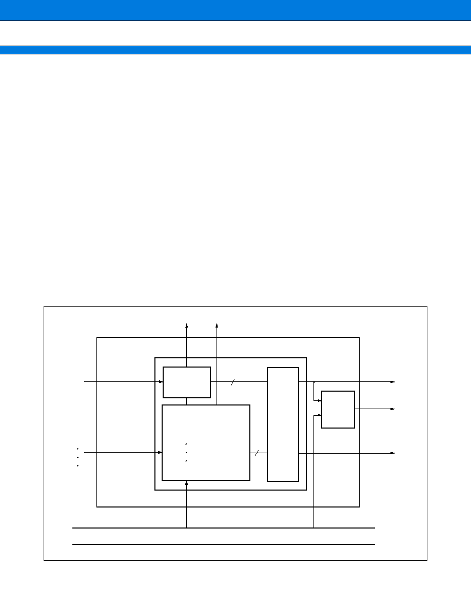
MB91340/MB91V340
59
3.
Interrupt Controller
The interrupt controller receives and processes interrupts.
∑
∑
∑
∑
Hardware Configuration
The interrupt controller consists of the following :
∑ ICR register
∑ Interrupt priority determination circuit
∑ Interrupt level and interrupt number (vector) generator
∑ Hold request removal request generator
∑
∑
∑
∑
Principal Functions
The main functions of the interrupt controller are as follows :
∑ Detect NMI and interrupt requests
∑ Prioritize interrupts (according to level and number)
∑ Notify interrupt level of selected interrupt request (to CPU)
∑ Notify interrupt number of selected interrupt request (to CPU)
If an NMI or interrupt request with an interrupt level other than "11111
B
" occurs, notify recovery from stop mode
(to CPU)
∑ Generate hold request removal requests to the bus master
∑
Block Diagram
RI00
RI47
(DLYIRQ)
5
6
LEVEL4
0
MHALTI
VCT5
0
R-BUS
UNMI
WAKEUP
ICR00
ICR47
("1" when LEVEL
11111
B
)
Determine order of priority
NMI
processing
LEVEL
determination
VECTOR
determination
LEVEL,
VECTOR
genera-
tion
HLDREQ
removal
request
MB91340/MB91V340
60
∑
Register List
(Continued)
Bit
Address :
Address :
Address :
Address :
Address :
Address :
Address :
Address :
Address :
Address :
Address :
Address :
Address :
Address :
Address :
Address :
Address :
Address :
Address :
Address :
Address :
Address :
Address :
Address :
Address :
Address :
Address :
Address :
Address :
Address :
Address :
Address :
7
6
5
4
3
2
1
0
ICR4
ICR3
ICR2
ICR1
ICR0
ICR4
ICR3
ICR2
ICR1
ICR0
ICR4
ICR3
ICR2
ICR1
ICR0
ICR4
ICR3
ICR2
ICR1
ICR0
ICR4
ICR3
ICR2
ICR1
ICR0
ICR4
ICR3
ICR2
ICR1
ICR0
ICR4
ICR3
ICR2
ICR1
ICR0
ICR4
ICR3
ICR2
ICR1
ICR0
ICR4
ICR3
ICR2
ICR1
ICR0
ICR4
ICR3
ICR2
ICR1
ICR0
ICR4
ICR3
ICR2
ICR1
ICR0
ICR4
ICR3
ICR2
ICR1
ICR0
ICR4
ICR3
ICR2
ICR1
ICR0
ICR4
ICR3
ICR2
ICR1
ICR0
ICR4
ICR3
ICR2
ICR1
ICR0
ICR4
ICR3
ICR2
ICR1
ICR0
ICR4
ICR3
ICR2
ICR1
ICR0
ICR4
ICR3
ICR2
ICR1
ICR0
ICR4
ICR3
ICR2
ICR1
ICR0
ICR4
ICR3
ICR2
ICR1
ICR0
ICR4
ICR3
ICR2
ICR1
ICR0
ICR4
ICR3
ICR2
ICR1
ICR0
ICR4
ICR3
ICR2
ICR1
ICR0
ICR4
ICR3
ICR2
ICR1
ICR0
ICR4
ICR3
ICR2
ICR1
ICR0
ICR4
ICR3
ICR2
ICR1
ICR0
ICR4
ICR3
ICR2
ICR1
ICR0
ICR4
ICR3
ICR2
ICR1
ICR0
ICR4
ICR3
ICR2
ICR1
ICR0
ICR4
ICR3
ICR2
ICR1
ICR0
ICR4
ICR3
ICR2
ICR1
ICR0
ICR4
ICR3
ICR2
ICR1
ICR0
ICR00
ICR01
ICR02
ICR03
ICR04
ICR05
ICR06
ICR07
ICR08
ICR09
ICR10
ICR11
ICR12
ICR13
ICR14
ICR15
ICR16
ICR17
ICR18
ICR19
ICR20
ICR21
ICR22
ICR23
ICR24
ICR25
ICR26
ICR27
ICR28
ICR29
ICR30
ICR31
00000440
H
00000441
H
00000442
H
00000443
H
00000444
H
00000445
H
00000446
H
00000447
H
00000448
H
00000449
H
0000044A
H
0000044B
H
0000044C
H
0000044D
H
0000044E
H
0000044F
H
00000450
H
00000451
H
00000452
H
00000453
H
00000454
H
00000455
H
00000456
H
00000457
H
00000458
H
00000459
H
0000045A
H
0000045B
H
0000045C
H
0000045D
H
0000045E
H
0000045F
H
R
R/W
R/W
R/W
R/W
MB91340/MB91V340
61
(Continued)
Bit
Address :
Address :
Address :
Address :
Address :
Address :
Address :
Address :
Address :
Address :
Address :
Address :
Address :
Address :
Address :
Address :
Address :
7
6
5
4
3
2
1
0
ICR4
ICR3
ICR2
ICR1
ICR0
ICR4
ICR3
ICR2
ICR1
ICR0
ICR4
ICR3
ICR2
ICR1
ICR0
ICR4
ICR3
ICR2
ICR1
ICR0
ICR4
ICR3
ICR2
ICR1
ICR0
ICR4
ICR3
ICR2
ICR1
ICR0
ICR4
ICR3
ICR2
ICR1
ICR0
ICR4
ICR3
ICR2
ICR1
ICR0
ICR4
ICR3
ICR2
ICR1
ICR0
ICR4
ICR3
ICR2
ICR1
ICR0
ICR4
ICR3
ICR2
ICR1
ICR0
ICR4
ICR3
ICR2
ICR1
ICR0
ICR4
ICR3
ICR2
ICR1
ICR0
ICR4
ICR3
ICR2
ICR1
ICR0
ICR4
ICR3
ICR2
ICR1
ICR0
ICR4
ICR3
ICR2
ICR1
ICR0
R
R/W
R/W
R/W
R/W
MHALTI
LVL4
LVL3
LVL2
LVL1
LVL0
R
R/W
R/W
R/W
R/W
R/W
ICR32
ICR33
ICR34
ICR35
ICR36
ICR37
ICR38
ICR39
ICR40
ICR41
ICR42
ICR43
ICR44
ICR45
ICR46
ICR47
HRCL
00000460
H
00000461
H
00000462
H
00000463
H
00000464
H
00000465
H
00000466
H
00000467
H
00000468
H
00000469
H
0000046A
H
0000046B
H
0000046C
H
0000046D
H
0000046E
H
0000046F
H
00000045
H
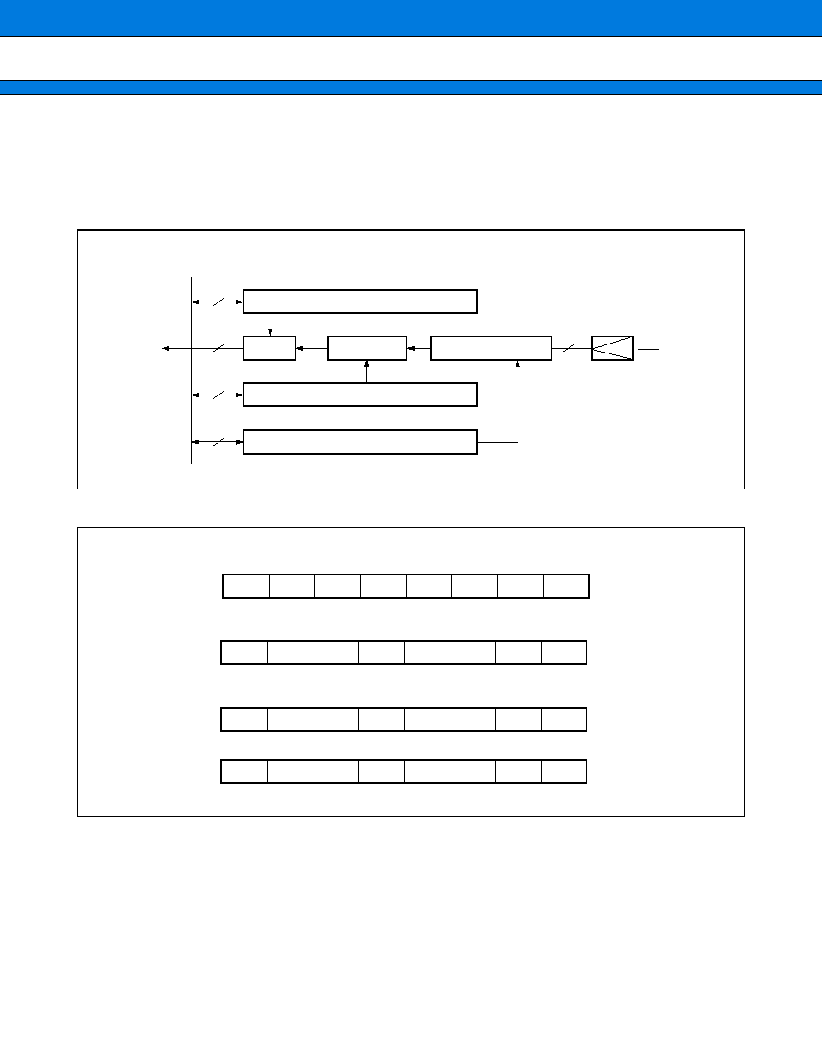
MB91340/MB91V340
62
4.
External Interrupt/NMI Control Block
The external interrupt control block controls external interrupt requests input to the NMIX and INT0-7 pins.
The interrupt trigger level can be selected from "H", "L", "rising edge", or "falling edge" (except for NMI).
∑
Block Diagram
∑
Register List
9
9
INT0
7
NMI
8
8
8
R BUS
Interrupt
request
Interrupt enable register
Gate
Request F/F
Edge detection circuit
Interrupt request register
Interrupt level setting register
External interrupt enable register (ENIR)
External interrupt request register (EIRR)
Request level setting register (ELVR)
bit
bit
bit
bit
7
6
5
4
3
2
1
0
EN6
EN7
EN5
EN4
EN3
EN2
EN1
EN0
15
14
13
12
11
10
9
8
ER6
ER7
ER5
ER4
ER3
ER2
ER1
ER0
15
14
13
12
11
10
9
8
LA7
LB7
LB6
LA6
LB5
LA5
LB4
LA4
7
6
5
4
3
2
1
0
LA3
LB3
LB2
LA2
LB1
LA1
LB0
LA0
MB91340/MB91V340
63
5.
REALOS Related Hardware
The REALOS hardware is used by the realtime operating system. Accordingly, these resources are not available
to the user program when REALOS is used.
5.1 Delay Interrupt Module
The delay interrupt module is used to generate interrupts for task switching.
This module can be used to generate and cancel interrupts to the CPU via software.
∑
Block Diagram
∑
Register List
DLYI
R-bus
Interrupt request
bit
Address : 00000044
H
DICR
7
6
5
4
3
2
1
0
[R/W]
DLYI
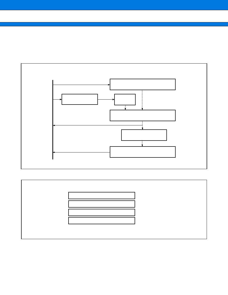
MB91340/MB91V340
64
5.2 Bit Search Module
Searches the data written to the input register for the first bit containing "0", "1", or a change in value. The module
returns the position of the detected bit.
∑
Block Diagram
∑
Register List
D-BUS
Address decoder
Input latch
Detection
mode
1 detection data capture
Bit search circuit
Search result
Address : 000003F0
H
"0" detection data register
Address : 000003F4
H
"1" detection data register
Address : 000003F8
H
Change bit detection data register
Address : 000003FC
H
Detection result register
31
BSD0
BSD1
BSDC
BSRR
0
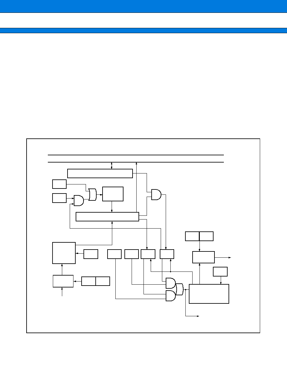
MB91340/MB91V340
65
6.
8-Bit Up Counter
The 8-bit up counter unit consists of an 8-bit up counter, 8-bit compare register, and their respective control
circuits.
The MB91340/MB91V340 has one 8-bit up counter channel.
∑
∑
∑
∑
8-Bit Up Counter Features
∑ The 8-bit count register can count in the range (0)d to (256)d.
∑ The count clock can be selected from four internal clocks (counts on the rising edge).
∑ Includes a compare function for performing up-counting.
∑ The interrupt generation frequency for compare match and overflow can be controlled.
∑ The compare match and overflow interrupt can be enabled and disabled independently.
∑ A clock can be generated by detecting the flag when a compare match or overflow occurs.
∑
Block Diagram
8 bit
8 bit
UCC
UCRE
CSTR
CLKS1 CLKS0
OVIE
CITE
OVFF
CMPF
IGR1
IGR0
FDCE
Data bus
COMPR (Compare register)
Counter
clear
UCR (Up count register)
Up
counter
Prescaler
Count clock
(CLKP)
Interrupt
generator
Interrupt request
Flag detection
counters
(IC3 to 0)
Outputs a flag detection
pulse (UCO) when compare
match or overflow occurs.
MB91340/MB91V340
66
∑
Register List
Up count register (UCR)
Compare register (COMPR)
Counter status register (CSR)
Counter control register (CCR)
bit
Address : 0000D3
H
bit
Address : 0000D1
H
bit
Address : 0000D2
H
bit
Address : 0000D0
H
15
8
CSR
7
0
31
24
CCR
UCR
COMPR
23
16
7
6
5
4
3
2
1
0
D06
D07
D05
D04
D03
D02
D01
D00
7
6
5
4
3
2
1
0
D06
D07
D05
D04
D03
D02
D01
D00
7
6
5
4
3
2
1
0
OVIE
CITE
CMPF
OVFF
IC3
IC2
IC1
IC0
7
6
5
4
3
2
1
0
CLKS1
CSTR
CLKS0
UCRE
UCC
FDCE
IGR1
IGR0
MB91340/MB91V340
67
7.
8/16-Bit Up/Down Counter/Timer
The 8/16-bit up/down counter/timer consists of an six event inputs, two 8-bit up/down counters, two 8-bit reload/
compare registers, and their various control circuits.
The MB91340/MB91V340 have four 8-bit up/down counter/timer channels.
∑
∑
∑
∑
8-Bit Up/Down Counter/Timer Features
Note : Phase difference count mode is suitable for use as a motor or similar encorder counter. High precision
rotational position and speed counters can be implemented easily by inputting the A, B and Z phase outputs
from the encoder.
Parameter
Function
Operation mode
∑ 8-bit 2 channel modes
∑ 16-bit 1 channel mode
Count mode
Can select four different count modes.
∑ Timer mode
∑ Up/down count mode
∑ Phase difference count mode (multiply by 2)
∑ Phase difference count mode (multiply by 4)
Count clock (In timer mode)
Can select two different count modes.
∑
/2 (
: Machine clock frequency)
∑
/8
Edge selection for detection
(In up/down count mode)
Can select which edge to detect on the external pin input signal.
∑ Edge detection disabled
∑ Detect falling edge
∑ Detect rising edge
∑ Detect both rising and falling edges
Function of ZIN pin
Can select two different functions.
∑ Counter clear function
∑ Gate function
Compare/reload function
Compare and reload functions are provided and these can be used individually or
together.
∑ Compare function (Interrupt request generation and counter clear by compare
match )
∑ Reload function (Interrupt request generation and reload by underflow)
∑ Compare/reload function (Interrupt request generation and counter clear by
compare match, interrupt request generation and reload by underflow)
∑ Compare/reload disabled
Count derection
∑ The direction of the most recent count operation can be determined from the
count direction flag.
Interrupt request
Can generate interrupt request
∑ Compare match
∑ Underflow or overflow
∑ Count direction change
MB91340/MB91V340
68
∑
Block Diagram
∑ 8/16-bit up/down counter/timer (ch0, 2)
CGE1
CGE0 CGEC
CTUT
UCRE
UDCC
CES1
CES0
CMS1
CCKS
CLKS
AIN0
ZIN0
BIN0
CMS0
CSTR
UDF1
UDF0
CDCF
UDFF
OVFF
CMPF
M16E
Carry
UDIE
CITE
CFIE
RLDE
8 bit
8 bit
Data bus
Edge/level detection
Up/down
count
clock
selection
Prescaler
UDCR0 (Up/down
count register 0)
Counter clear
Reload
control
RCR0 (Reload/
compare register 0)
Interrupt output
To ch1, 3
Count
clock
Input from up
counter
UDD
register
MB91340/MB91V340
69
∑
8/16-bit up/down counter/timer (ch1, 3)
CGE1
CGE0 CGEC
CTUT
UCRE
UDCC
CES1
CES0
CMS1
CCKS
CLKS
AIN1
ZIN1
BIN1
CMS0
CSTR
UDF1
UDF0
CDCF
UDFF
OVFF
CMPF
UDD
UDIE
CITE
CFIE
RLDE
8 bit
8 bit
Carry
M16E
Data bus
Edge/level detection
UDCR1 (Up/down
count register 1)
RCR1 (Reload/
compare register 1)
Interrupt output
Up/down
count
clock
selection
Count
clock
Input from up
counter
Prescaler
Counter clear
Reload
control
To ch0, 2
MB91340/MB91V340
70
∑
Register List
(Continued)
Up/down count register (UDCR)
∑ Up/down count register ch0 (UDCR0)
∑ Up/down count register ch1 (UDCR1)
∑ Up/down count register ch2 (UDCR2)
∑ Up/down count register ch3 (UDCR3)
Reload/compare register (RCR)
∑ Reload/compare register ch0 (RCR0)
∑ Reload/compare register ch1 (RCR1)
∑ Reload/compare register ch2 (RCR2)
∑ Reload/compare register ch3 (RCR3)
bit
Address : 0000B3
H
bit
Address : 0000B2
H
bit
Address : 0000BF
H
bit
Address : 0000BE
H
bit
Address : 0000B1
H
bit
Address : 0000B0
H
bit
Address : 0000BD
H
bit
Address : 0000BC
H
15
8
UDCR1
7
0
31
24
RCR1
UDCR0
RCR0
CCRH0
CSR0
CCRL0
CCRH1
CSR1
CCRL1
UDCR3
RCR3
UDCR2
RCR2
CCRH2
CSR2
CCRL2
CCRH3
CSR3
CCRL3
23
16
7
6
5
4
3
2
1
0
D06
D07
D05
D04
D03
D02
D01
D00
15
14
13
12
11
10
9
8
D14
D15
D13
D12
D11
D10
D09
D08
7
6
5
4
3
2
1
0
D06
D07
D05
D04
D03
D02
D01
D00
15
14
13
12
11
10
9
8
D14
D15
D13
D12
D11
D10
D09
D08
7
6
5
4
3
2
1
0
D06
D07
D05
D04
D03
D02
D01
D00
15
14
13
12
11
10
9
8
D14
D15
D13
D12
D11
D10
D09
D08
7
6
5
4
3
2
1
0
D06
D07
D05
D04
D03
D02
D01
D00
15
14
13
12
11
10
9
8
D14
D15
D13
D12
D11
D10
D09
D08

MB91340/MB91V340
71
(Continued)
Counter status register (CSR)
∑ Counter status register ch0, 1 (CSR0, 1)
∑ Counter status register ch2, 3 (CSR2, 3)
Counter control register (CCRL)
∑ Counter control register ch0, 1 (CCRL0, 1)
∑ Counter control register ch2, 3 (CCRL2, 3)
Counter control register (CCRH)
∑ Counter control register ch0 (CCRH0)
∑ Counter control register ch1 (CCRH1)
∑ Counter control register ch2 (CCRH2)
∑ Counter control register ch3 (CCRH3)
bit
Address :
0000B7
H
0000BB
H
bit
Address :
0000C3
H
0000C7
H
bit
Address :
0000B5
H
0000B9
H
bit
Address :
0000C1
H
0000C5
H
bit
Address : 0000B4
H
bit
Address : 0000B8
H
bit
Address : 0000C0
H
bit
Address : 0000C4
H
7
6
5
4
3
2
1
0
CITE
CSTR
UDIE
CMPF
OVFF
UDFF
UDF1
UDF0
7
6
5
4
3
2
1
0
CITE
CSTR
UDIE
CMPF
OVFF
UDFF
UDF1
UDF0
7
6
5
4
3
2
1
0
CTUT
CCKS
UCRE
RLDE
UDCC
CGSC
CGE1
CGE0
7
6
5
4
3
2
1
0
CTUT
CCKS
UCRE
RLDE
UDCC
CGSC
CGE1
CGE0
15
14
13
12
11
10
9
8
CDCF
M16E
CFIE
CLKS
CMS1
CMS0
CES1
CES0
15
14
13
12
11
10
9
8
CDCF
UDD
CFIE
CLKS
CMS1
CMS0
CES1
CES0
15
14
13
12
11
10
9
8
CDCF
M16E
CFIE
CLKS
CMS1
CMS0
CES1
CES0
15
14
13
12
11
10
9
8
CDCF
UDD
CFIE
CLKS
CMS1
CMS0
CES1
CES0
MB91340/MB91V340
72
8.
16-Bit Reload Timer
The 16-bit timer consists of a 16-bit down-counter, 16-bit reload register, prescaler for generating the internal
count clock, and a control register.
The clock source can be selected from three internal clock signals (machine clock divided by 2, 8, or 32 - ch3
also supports machine clock divided by 64 or 128) or the external event input.
The interrupt can be used to initiate DMA transfer.
The MB91340/MB91V340 has four 16-bit reload timer channels.
∑
Block Diagram
∑
Register List
∑ Control status register (TMCSR)
∑ 16-bit timer register (TMR)
∑ 16-bit reload register (TMRLR)
RELD
OUTL
INTE
UF
CNTE
TRG
OUT
CTL.
CSL2
CSL1
CSL0
MOD2
MOD1
MOD0
16
7
16
3
3
IN CTL.
SLT
TOE0 ~ 3
2
2
2
1
3
5
3
EXCK
IRQ
2
2
6
7
R
|
B
U
S
16-bit reload register (TMRLR)
16-bit down counter (TMR) UF
Reload
Clock selector
Re-trigger
Prescaler
clear
Machine clock input
(CLKP)
8-bit up counter (ch3 only)
External trigger input (TIN0 to 3)
External
trigger
selection
(ch3 only)
To external timer outputs
(TOT0 to 3)
Bit located in PFRK
Count enable
(ch3 only)
15
14
13
12
11
10
9
8
CSL2
CSL1
CSL0
MOD2
MOD1
SLT
7
6
5
4
3
2
1
0
MOD0
OUTL
RELD
INTE
UF
CNTE
TRG
15
0
15
0
MB91340/MB91V340
73
9.
U-TIMER (16 bit timer for UART baud rate generation)
The U-TIMER is a 16-bit timer used to generate the baud rate for the UART. Any desired baud rate can be set
using the combination of the chip operating frequency and U-TIMER reload value.
The U-TIMER can also be used as an interval timer by generating an interrupt from a count underflow event.
The MB91340/MB91V340 has three U-TIMER channels. When used as an interval timer, two U-TIMER channels
can be connected in cascade for a maximum count interval of up to 2
32
◊
.
Cascade connection is only available for channel 0 and channel 1 or channel 0 and channel 2.
∑
Block Diagram
∑
Register List
UTIMR (reload register)
UTIM (timer)
clock
load
underflow
under flow U-TIMER 1
to UART
control
f.f.
15
15
0
0
MUX
Channel 0
only
(CLKP)
(Peripheral clock)
UTIMR
UTIM
UTIMC
(W)
(R)
(R/W)
15
0
8 7

MB91340/MB91V340
74
10. UART
The UART is a serial I/O port for asynchronous (start-stop synchronized) or CLK synchronized transmission.
The MB91340/MB91V340 has three UART channels.
∑
∑
∑
∑
UART Features
∑ Full duplex double buffer
∑ Asynchronous (start-stop synchronized) or CLK synchronized transmission
∑ Supports multi-processor mode
∑ Fully programmable baud rate
The internal timer can be set to any desired baud rate (see U-TIMER description)
∑ Variable baud rate can be input from an external clock.
∑ Error detection functions (parity, framing, overrun)
∑ Transmission signal format is NRZ
∑ The interrupt can be used to initiate DMA transfer.
∑ The DMAC interrupt can be cleared by writing to the DRCL register.
MB91340/MB91V340
75
∑
Block Diagram
MD1
MD0
CS0
SCKE
PEN
P
SBL
CL
A
/
D
REC
RXE
TXE
PE
ORE
FRE
RDRF
TDRE
BDS
RIE
TIE
R - BUS
SIDR
SODR
Control signal
From U-TIMER
External clock
SCK
Clock
selection
circuit
Receive status
decision circuit
Receive error
signal for DMA
(to DMAC)
RX clock
RX control circuit
Start bit detect
circuit
Receive bit
counter
Receive parity
counter
RX shifter
RX
complete
TX clock
RX interrupt
(to CPU)
TX interrupt
(to CPU)
TX control circuit
TX start
circuit
Send bit
counter
Send parity
counter
TX shifter
TX start
SMR
register
Control
signal
SCR
register
SSR
register
SCK (clock)
SI (Receive data)
SO (Send data)
MB91340/MB91V340
76
∑
Register List
Register List Serial output register (SIDR/SODR)
Serial status register (SSR)
Serial mode register (SMR)
Serial control register (SCR)
(DRCL)
SIDR (R)/SODR (W)
SMR
SCR
(R/W)
(R/W)
(W)
SSR
DRCL
8 bit
8 bit
15
0
8 7
7
6
5
4
3
2
1
0
D6
D7
D5
D4
D3
D2
D1
D0
7
6
5
4
3
2
1
0
ORE
PE
FRE
RDRF
TDRE
BDS
RIE
TIE
7
6
5
4
3
2
1
0
MD0
MD1
CS0
SCKE
7
6
5
4
3
2
1
0
P
PEN
SBL
CL
A/D
REC
RXE
TXE
7
6
5
4
3
2
1
0
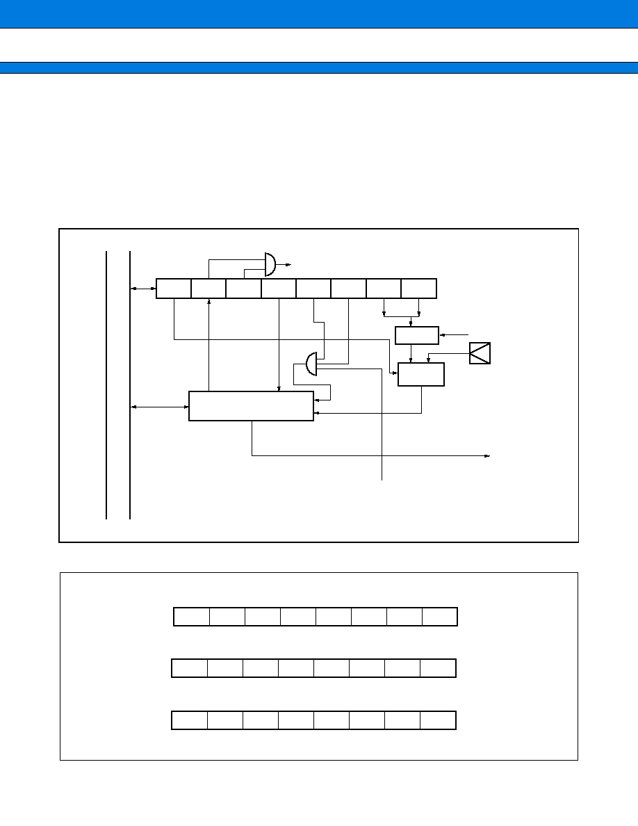
MB91340/MB91V340
77
11. 16-Bit Freerun Timer
The 16-bit freerun timer consist of a 16-bit up counter and control status register.
The count value from the 16-bit freerun timer is used as the base time for the output compare and input capture.
The count clock can be selected from four different clocks.
An interrupt can be generated when a counter overflow occurs.
A mode setting is available that initializes the counter when a match with the value in compare register 0 (in the
output compare unit) occurs.
∑
Block Diagram
∑
Register List (upper)
ECLK
IVF
IVFE
STOP
MODE
CLR
CLK1
CLK0
(CLKP)
R-B
US
Overflow interrupt request
for 16-bit freerun timer
16-bit freerun timer
(TCDT)
Divider
Clock
selection
FRCK
Input pin
Output counter value to input
capture and output compare
(T15 to T00)
Signal indicating a match with
output compare register 0
Clock
Timer data register
Timer data register (lower) (TCDT)
Timer control status register (lower) (TCCS)
15
14
13
12
11
10
9
8
T14
T15
T13
T12
T11
T10
T09
T08
7
6
5
4
3
2
1
0
T06
T07
T05
T04
T03
T02
T01
T00
7
6
5
4
3
2
1
0
IVF
ECLK
IVFE
STOP
MODE
CLR
CLK1
CLK0
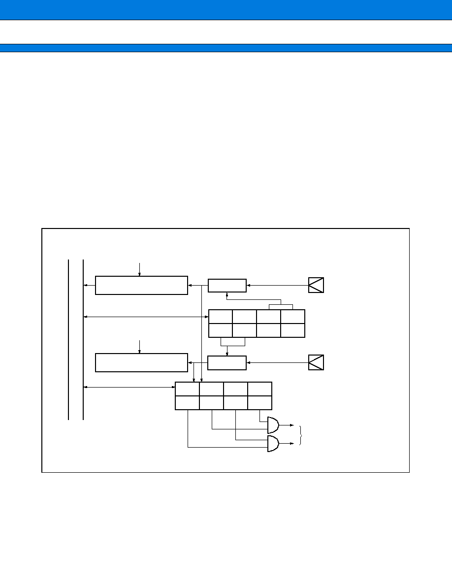
MB91340/MB91V340
78
12. Input Capture
The input capture unit detects rising edges, falling edges, or either edge on the signal input from an external pin
and saves the value of the 16-bit freerun timer at that time to a register. The unit can also generate an interrupt
when an edge is detected.
The input capture consists of an input capture data register and control register.
Each input capture channel has its own external input pin.
The active edge on the external input can be selected from the following three options :
∑ Riding edge
∑ Falling edge
∑ Either edge
The input capture can generate an interrupt when an active edge is detected.
The MB91340/MB91V340 has four input capture channels.
∑
Block Diagram
EG11
EG10
EG01
EG00
EG31
EG30
EG21
EG20
ICP1
ICP0
ICE1
ICE0
ICP3
ICP2
ICE3
ICE2
R-B
US
Counter value from 16-bit
freerun timer (T15 to T00)
Capture data register
ch (0, 2)
Counter value from 16-bit
freerun timer (T15 to T00)
Capture data register
ch (1, 3)
Edge
detection
Edge
detection
IN0, 2
Input pin
IN1, 3
Input pin
Input capture interrupt
request
MB91340/MB91V340
79
∑
Register List
Input capture data register (upper) (IPCP)
Input capture data register (lower) (IPCP)
Capture control register (ICS23)
Capture control register (ICS01)
15
14
13
12
11
10
9
8
CP14
CP15
CP13
CP12
CP11
CP10
CP09
CP08
7
6
5
4
3
2
1
0
CP06
CP07
CP05
CP04
CP03
CP02
CP01
CP00
7
6
5
4
3
2
1
0
ICP2
ICP3
ICE3
ICE2
EG31
EG30
EG21
EG20
7
6
5
4
3
2
1
0
ICP0
ICP1
ICE1
ICE0
EG11
EG10
EG01
EG00
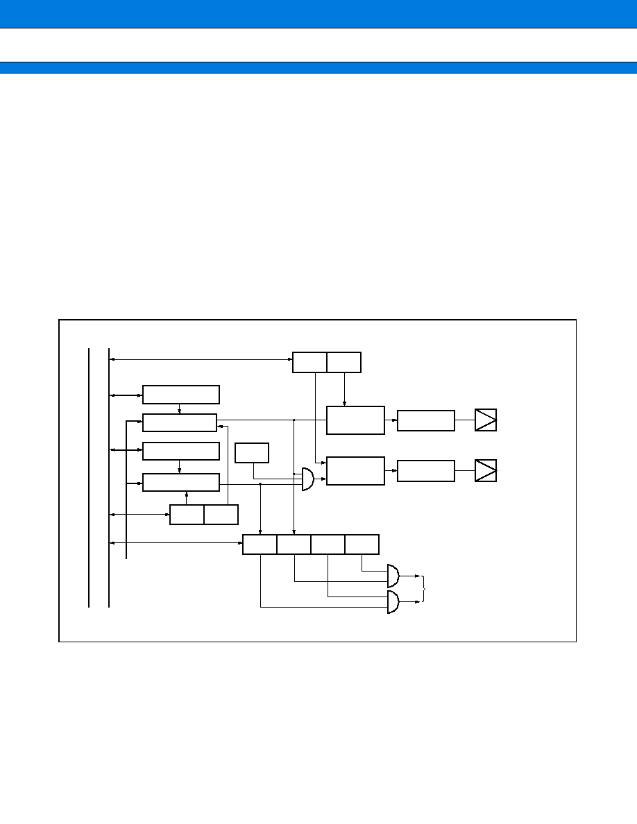
MB91340/MB91V340
80
13. Output Compare
The output compare unit consists of a 16-bit compare register, compare output latch, and control register. The
unit can toggle the output level and generate an interrupt when a match occurs between the 16-bit freerun timer
and compare register.
The MB91340/MB91V340 has eight output compare channels.
Output Compare Features
∑ The eight compare registers operate independently. Each compare register has its own output pin and interrupt
flag.
∑ Two compare registers can be used together to control an output pin. The output pin is toggled by both registers.
∑ The initial value of each output pin can be specified.
∑ An interrupt is generated when a compare match occurs.
∑ The ch0 compare register can be used to clear the 16-bit freerun timer.
∑
Block Diagram
ICP1
ICP0
ICE1
ICE0
ODT1
ODT0
CST1
CST0
CMOD
OTE0, 2, 4, 6
OTE1, 3, 5, 7
R-B
US
(The ch0 register only can be used
to clear the 16-bit freerun timer.)
Compare register
Compare circuit
Compare register
Compare circuit
16-bit freerun timer value
Output compare
interrupt request
Compare
output latch
Compare
output latch
OTE0 to 7 are in
PFRO register
Output pin
(ch0, 2, 4, 6)
Output pin
(ch1, 3, 5, 7)
MB91340/MB91V340
81
∑
Register List
Compare register (upper) (OCCP)
Compare register (lower) (OCCP)
Output control register (upper) (OCS)
Output control register (lower) (OCS)
15
14
13
12
11
10
9
8
C14
C15
C13
C12
C11
C10
C09
C08
7
6
5
4
3
2
1
0
C06
C07
C05
C04
C03
C02
C01
C00
15
14
13
12
11
10
9
8
CMOD
OTD1
OTD0
7
6
5
4
3
2
1
0
ICP0
ICP1
ICE1
ICE0
CST1
CST0

MB91340/MB91V340
82
14. I
2
C Interface
The I
2
C interface is a serial port that supports the Inter IC Bus protocol. It can operate as a master or slave
device on the I
2
C bus.
I
2
C Interface Features
∑ Master/slave send and receive
∑ Arbitration function
∑ Clock synchronization function
∑ Slave address and general call address detection function
∑ Transmission direction detection function
∑ Repeated "START" condition generation and detection function
∑ Bus error detection function
∑ 10-bit or 7-bit slave address
∑ Slave address receive acknowledge control when in master mode
∑ Supports compound slave addresses
∑ Can generate an interrupt on transmission or bus error
∑ Supports standard mode (100 Kbps Max) and high-speed mode (400 Kbps Max)
∑ Both "standard mode" and "terminal split mode" external pins provided.
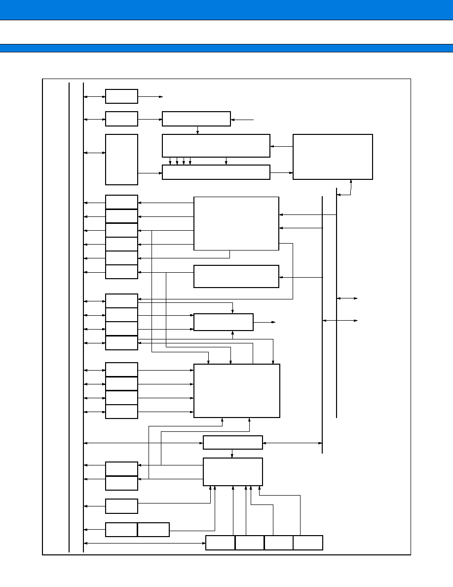
MB91340/MB91V340
83
∑
Block Diagram
ICCR
EN
IDBL
DBL
ICCR
IBSR
BB
RSC
LRB
Last Bit
TRX
ADT
AL
IBCR
BER
BEIE
INTE
INT
IBCR
SCC
MSS
ACK
GCAA
IBSR
ISMK
ITMK
IDAR
AAS
GCA
FNSB
ENTB
RAL
ITBA
ITMK
ISBA
ISMK
CS4
CS3
CS2
CS1
CS0
2 3 4 5
32
Sync
(CLKP)
First Byte
IRQ
SCL
SCLI
SCLO
SDA
SDAI
SDAO
I
2
C operation enable
Clock enable
Clock divider 2
Clock selection 2 (1/12)
Bus busy
Repeat start
TX/RX
Start stop condition
generation
Arbitration lost detection
Interrupt request
Start
Master
ACK OK
GC-ACK OK
Slave
Global call
Slave address
compare
End
Error
Shift clock edge
change timing
Start stop condition
detection
Shift clock generator
R bus
MB91340/MB91V340
84
∑
Register List
(Continued)
∑
Bus control register (IBCR)
∑
Bus status register (IBSR)
∑
10-bit slave address register (ITBA)
∑
10-bit slave address mask register (ITMK)
∑
7-bit slave address register (ISBA)
∑
7-bit slave address mask register (ISMK)
Address : 000094
H
Initial value
Address
: 000095
H
Initial value
Address
: 000096
H
Initial value
Address
: 000097
H
Initial value
Address
: 000098
H
Initial value
Address
: 000099
H
Initial value
Address
: 00009B
H
Initial value
Address
: 00009A
H
Initial value
R/W
0
W
0
R/W
0
R/W
0
R/W
0
R/W
0
R/W
0
15
14
13
12
11
10
9
8
BEIE
R/W
0
BER
SCC
MSS
ACK
GCAA
INTE
INT
R
0
R
0
R
0
R
0
R
0
R
0
R
0
7
6
5
4
3
2
1
0
RSC
R
0
BB
AL
LRB
TRX
AAS
GCA
ADT
R/W
0
R/W
0
15
14
13
12
11
10
9
8
TA9
TA8
R/W
0
R/W
0
R/W
0
R/W
0
R/W
0
R/W
0
R/W
0
7
6
5
4
3
2
1
0
TA6
R/W
0
TA7
TA5
TA4
TA3
TA2
TA1
TA0
R
0
R/W
1
R/W
1
15
14
13
12
11
10
9
8
RAL
R/W
0
ENTB
TM9
TM8
R/W
1
R/W
1
R/W
1
R/W
1
R/W
1
R/W
1
R/W
1
7
6
5
4
3
2
1
0
TM6
R/W
1
TM7
TM5
TM4
TM3
TM2
TM1
TM0
R/W
0
R/W
0
R/W
0
R/W
0
R/W
0
R/W
0
R/W
0
7
6
5
4
3
2
1
0
SA6
SA5
SA4
SA3
SA2
SA1
SA0
R/W
1
R/W
1
R/W
1
R/W
1
R/W
1
R/W
1
R/W
1
15
14
13
12
11
10
9
8
SM6
R/W
0
ENSB
SM5
SM4
SM3
SM2
SM1
SM0
MB91340/MB91V340
85
(Continued)
∑
Data register (IDAR)
∑
Clock control register (ICCR)
∑
Clock disable register (IDBL)
Address : 00009D
H
Initial value
Address : 00009E
H
Initial value
Address : 00009F
H
Initial value
R/W
0
R/W
0
R/W
0
R/W
0
R/W
0
R/W
0
R/W
0
7
6
5
4
3
2
1
0
D6
R/W
0
D7
D5
D4
D3
D2
D1
D0
R/W
0
R/W
1
R/W
1
R/W
1
R/W
1
R/W
1
15
14
13
12
11
10
9
8
W
0
TEST
EN
CS4
CS3
CS2
CS1
CS0
R/W
0
7
6
5
4
3
2
1
0
DBL
MB91340/MB91V340
86
15. A/D Converter (Successive Approximation Type)
The A/D converter converts analog input voltages to digital values.
∑
∑
∑
∑
A/D Converter Features
∑ Minimum conversion time 5.4
µ
s/ch (for machine clock
=
33 MHz-CLKP)
∑ Internal sample & hold circuit
∑ Resolution
=
10-bit ( 8-bit accuracy)
∑ 8 program-selectable analog inputs
Single conversion mode : Convert 1 specified channel
Scan conversion mode : ontinuous conversion of multiple channels. Conversion can be specified for up to
8 channels.
∑ Single, continuous, and stop conversion operation is supported.
Single mode: Convert specified channel then stop.
Continuous conversion mode: Perform continuous conversion for the selected channel.
Stop conversion mode: Perform conversion for one channel, then wait for the next activation
trigger (synchronizes the conversion start timing)
∑ DMA transfer can be initiated by an interrupt.
∑ Selectable conversion activation trigger: Software, external trigger (falling edge), or reload timer (rising edge)
∑
Block Diagram
AV
CC
AN0
AN1
AN2
AN3
AN4
AN5
AN6
AN7
AVRH
AV
SS
R
|
B
U
S
Input switch
Sample & hold circuit
Channel decoder
Internal voltage
generator
Successive
approximation register
Data register
(ADCR : 10 bit)
A/D control register
(ADCS)
ATG (External pin trigger)
Reload timer ch2
(internal connection)
Timing generation circuit
Prescaler
Machine clock
(CLKP)
Data register
(ADCR0 to 7 : 8 bit)
Upper 8 bit COPY
MB91340/MB91V340
87
∑
Register List
Control status register (ADCS)
Data register (ADCR)
Conversion result register (ADCR0 to 7)
bit
bit
bit
bit
bit
15
14
13
12
11
10
9
8
INT
BUSY
INTE
CRF
STS1
STS0
STRT
7
6
5
4
3
2
1
0
MD0
MD1
ANS2
ANS1
ANS0
ANE2
ANE1
ANE0
15
14
13
12
11
10
9
8
9
8
7
6
5
4
3
2
1
0
6
7
5
4
3
2
1
0
7
6
5
4
3
2
1
0
6
7
5
4
3
2
1
0
MB91340/MB91V340
88
16. 8-Bit D/A Converter
The 8-bit D/A converter consists of three D/A converter channels with 8-bit resolution and independent outputs
controlled by the D/A control register.
∑
∑
∑
∑
8-bit D/A Converter Features
∑ Includes power-down function
∑ Operation : Max 200 kSPS
∑ Power consumption 2.3 mW (Typ)
∑ 3.3 V interface
∑
Block Diagram
∑
Register List
DTE
WDR0
DAE0
PD
R bus
DTE
WDR1
DAE1
PD
GND
GND
DAE2
PD
D/A control
register
D/A data
register 0
D/A data
register 1
D/A data
register 2
D/A
converter
D/A
converter
D/A
converter
D/A output 0
(DA0)
D/A output 1
(DA1)
D/A output 2
(DA2)
D/A data register 0 to 2 (DADR0 to 2)
D/A control register 0 to 2 (DACR0 to 2)
bit
bit
7
6
5
4
3
2
1
0
DA6
DA7
DA5
DA4
DA3
DA2
DA1
DA0
7
6
5
4
3
2
1
0
DAE
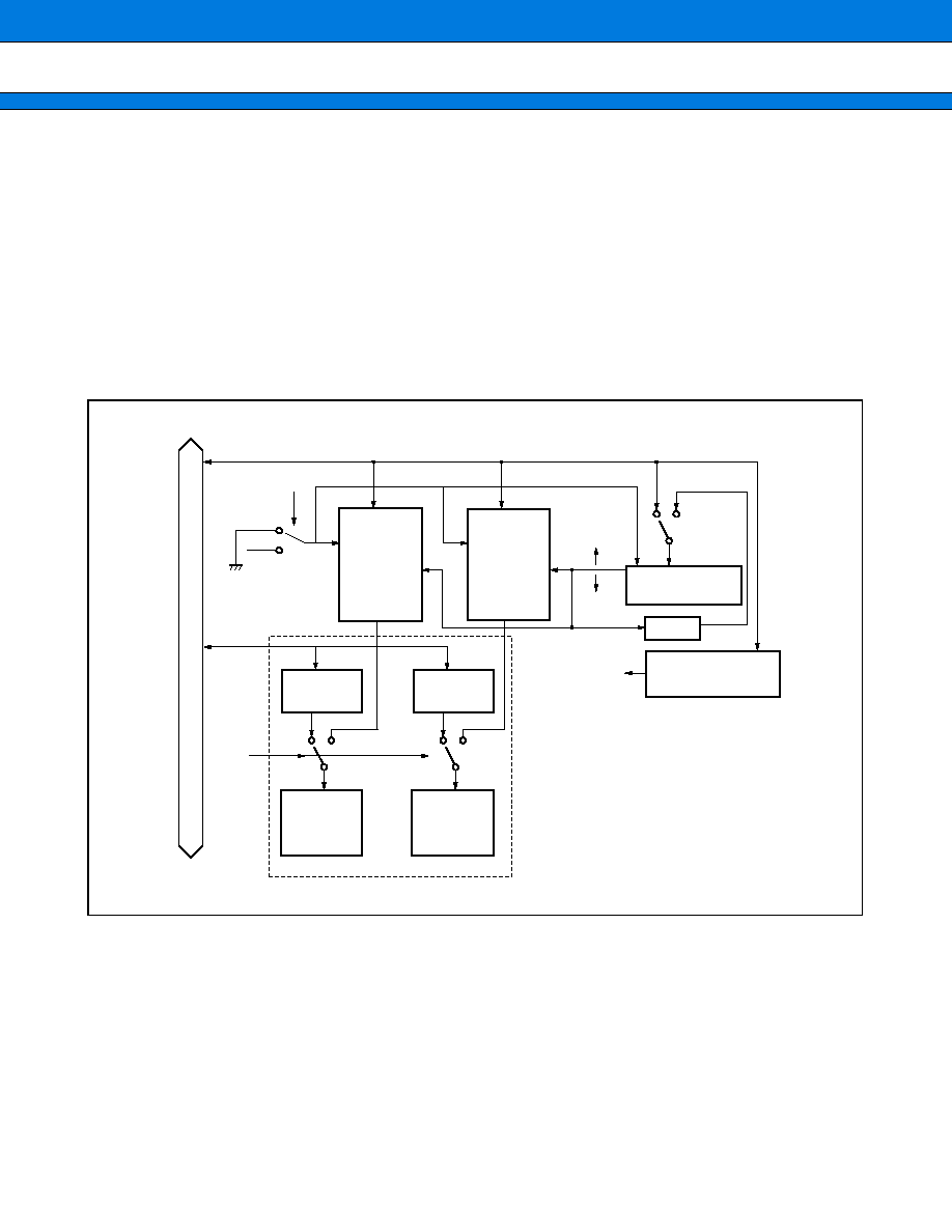
MB91340/MB91V340
89
17. Waveform Data Transfer
The waveform data transfer consists of two 64 byte registers used to transfer data to their corresponding D/A
converters.
∑
∑
∑
∑
Waveform Data Transfer Features
∑ The pulse output of the 8-bit up counter is used as the transfer clock.
∑ The speed of transfer to the D/A converter can be controlled by changing the frequency of the 8-bit up counter
pulse output.
∑ Forward or reverse direction can be specified.
∑
Block Diagram
R_bus
R_bus
DTE
DTE
CLK
CLK
CLK
DIR
=
1
DTE, DIR
DIR
=
0
±
1
Transfer
data
register 0
(64 byte)
Transfer
data
register 1
(64 byte)
Address pointer
register
Waveform control
register
D/A data
register 0
D/A
converter
D/A data
register 1
D/A
converter
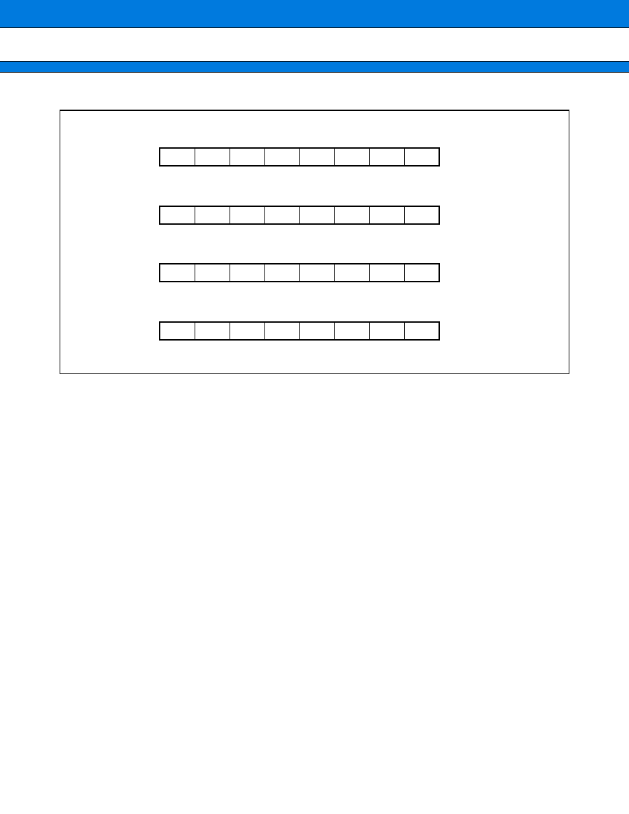
MB91340/MB91V340
90
∑
Register List
Waveform control register (WCR)
Address pointer register (APR)
Waveform data register (WDR1)
Waveform data register (WDR0)
7
6
5
4
3
2
1
0
R/W
DIR
DTE
EA5
EA4
R/W
EA3
EA2
EA1
R/W
R/W
R/W
R/W
R/W
R/W
EA0
7
6
5
4
3
2
1
0
R/W
AI
AP5
AP4
R/W
AP3
AP2
AP1
R/W
R/W
R/W
R/W
R/W
AP0
15
14
13
12
11
10
9
8
R/W
WD16
WD17
WD15
WD14
R/W
WD13
WD12
WD11
R/W
R/W
R/W
R/W
R/W
R/W
WD10
7
6
5
4
3
2
1
0
WD06
WD07
WD05
WD04
WD03
WD02
WD01
WD00

MB91340/MB91V340
91
18. Version Register
The version register is a 4-bit internal register.
The version register can be read to determine the device version.
∑
Register List
Version register (VERR)
7
6
5
4
3
2
1
0
VR3
VR2
VR1
VR0

MB91340/MB91V340
92
19. DMAC (DMA Controller)
The DMA controller is used to perform DMA (direct memory access) transfer on the FR series device.
Using DMA transfer under the control of the DMA controller improves system performance by enabling data to
be transferred at high speed independently of the CPU.
∑
∑
∑
∑
Hardware Configuration
∑ 5 independent DMA channels
◊
5 ch
∑ 5 independent access control circuits
∑ 32-bit address register (Supports reloading : 2 per channel)
∑ 16-bit transfer count register (Supports reloading : 1 per channel)
∑ 4-bit block count register (1 per channel)
∑ External transfer request input pins : DREQ0, DREQ1, DREQ2 (ch0, 1, 2 only)
∑ External transfer request acknowledge output pins : DACK0, DACK1, DACK2 (ch0, 1, 2 only)
∑ DMA completion output pins : DEOP0, DEOP1, DEOP2 (ch0, 1, 2 only)
∑ fly-by transfer (memory to I/O , I/O to memory) (ch0, 1, 2 only)
∑ Two-cycle transfer
∑
∑
∑
∑
Main Functions of the DMA Controller
∑ Supports independent data transfer for multiple channels (5 channels)
(1) Priority order (ch.0
>
ch.1
>
ch.2
>
ch.3
>
ch.4)
(2) Order can be reversed for ch0 and ch1
(3) DMAC activation triggers
∑
Input from dedicated external pin (edge detection/level detection, ch0,1,2 only)
∑
Request from internal peripheral (shared interrupt request, including external interrupts)
∑
Software request (register write)
(4) Transfer modes
∑
Demand transfer, burst transfer, step transfer, or block transfer
Addressing mode: Full 32-bit address (increment/decrement/fixed)
(address increment can be in the range
-
255 to
+
255)
∑
Data type : byte/half-word/word
∑
Single-shot or reload operation selectable
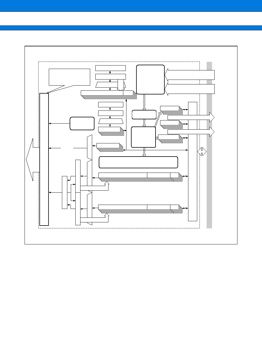
MB91340/MB91V340
93
∑
Block Diagram
Read
Write
DDNO
BLK register
DDNO register
DTCR
DSS [3:0]
ERIR, EDIR
TYPE, MOD, WS
IRQ
[4:0]
MCLREQ
X-bus
DADM, DASZ [7:0] DADR
SDAM, SASZ [7:0] SADR
DMA transfer
request to bus
controller
Read/write
control
To bus
controller
Bus control block
Access
ad-
dress
Addr
ess counter
Counter buffer
Counter buffer
Selector
Selector
Write back
Selector
Buffer
Counter
Selector
Write back
DTC two-stage register
Buffer
Counter
Selector
DMA
start trigger
selection cir-
cuit & request
acknowledge
control
Priority
circuit
Status
transition
circuit
DMA control
DSAD two-stage register
DDAD
two-stage register
Bus control block
Peripheral start request/
Stop input
External pin start
request/Stop input
To interrupt controller
Clear peripheral interrupt
5-channel DMAC block diagram
Write back
MB91340/MB91V340
94
∑
Register List
ch.0 control/status
register A
ch.0 control/status
register B
ch.1 control/status
register A
ch.1 control/status
register B
ch.2 control/status
register A
ch.2 control/status
register B
ch.3 control/status
register A
ch.3 control/status
register B
ch.4 control/status
register A
ch.4 control/status
register B
Overall control register
ch.0 transfer source address register
ch.0 transfer destination address register
ch.1 transfer source address register
ch.1 transfer destination address register
ch.2 transfer source address register
ch.2 transfer destination address register
ch.3 transfer source address register
ch.3 transfer destination address register
ch.4 transfer source address register
ch.4 transfer destination address register
(bit) 31
24 23
16 15
08 07
00
(bit) 31
24 23
16 15
08 07
00
0000200
H
0000204
H
0000208
H
000020C
H
0000210
H
0000214
H
0000218
H
000021C
H
0000220
H
0000224
H
0000240
H
0001000
H
0001004
H
0001008
H
000100C
H
0001010
H
0001014
H
0001018
H
000101C
H
0001020
H
0001024
H
DMACA0
DMACB0
DMACA1
DMACB1
DMACA2
DMACB2
DMACA3
DMACB3
DMACA4
DMACB4
D M A C R
DMASA0
DMADA0
DMASA1
DMADA1
DMASA2
DMADA2
DMASA3
DMADA3
DMASA4
DMADA4
MB91340/MB91V340
95
20. Clock Generation Control
The internal operating clock is generated as follows in MB91340/MB91V340.
∑
Source clock selection : Selects the clock source.
∑
Base clock generation : The base clock is generated by dividing the source clock by 2 or using a PLL.
∑
Generation in each internal block : The base clock is divided to generate the operating clock for each block.
∑
Register List
(Continued)
∑
RSRR : Reset initiation register/Watchdog timer control register
"*" : Changes depending on what triggered the reset.
"
◊
" : Not initialized
∑
STCR : Standby control register
* : Only when asserted during a reset initiated by the INIT pin. Otherwise, same as INIT.
bit
address : 00000480
H
Initial value (INIT pin)
Initial value (INIT)
Initial value (RST)
bit
address : 00000481
H
Initial value (INIT pin)
Initial value (HST) *
Initial value (INIT)
Initial value (RST)
R
0
X
R
0
X
R
0
X
R/W
0
0
0
R/W
0
0
0
15
14
13
12
11
10
9
8
HSTB
R
1
X
INIT
WDOG
SRST
WT1
WT0
R/W
0
0
0
0
R/W
1
1
1
X
R/W
1
1
1
1
R/W
0
1
X
X
R/W
0
1
X
X
R/W
1
1
1
X
7
6
5
4
3
2
1
0
SLEEP
R/W
0
0
0
0
STOP
HIZ
SRST
OS1
OS0
OSCD1
MB91340/MB91V340
96
(Continued)
∑
TBCR : Timebase counter control register
∑
CTBR : Timebase counter clear register
∑
CLKR : Clock source control register
∑
WPR : Watchdog reset generation delay register
∑
DIVR0 : Base clock division setting register 0
∑
DIVR1 : Base clock division setting register 1
bit
address : 00000482
H
Initial value (INIT)
Initial value (RST)
bit
address : 00000483
H
Initial value (INIT)
Initial value (RST)
bit
address : 00000484
H
Initial value (INIT)
Initial value (RST)
bit
address : 00000485
H
Initial value (INIT)
Initial value (RST)
bit
address : 00000486
H
Initial value (INIT)
Initial value (RST)
bit
address : 00000487
H
Initial value (INIT)
Initial value (RST)
0
0
R/W
X
X
R/W
X
X
R/W
X
X
R/W
0
X
R/W
0
X
R/W
15
14
13
12
11
10
9
8
TBIE
0
0
R/W
TBIF
TBC2
TBC1
TBC0
SYNCR SYNCS
X
X
W
X
X
W
X
X
W
X
X
W
X
X
W
X
X
W
X
X
W
7
6
5
4
3
2
1
0
D6
X
X
W
D7
D5
D4
D3
D2
D1
D0
R/W
0
X
R/W
0
X
R/W
0
X
R/W
0
X
R/W
0
X
R/W
0
X
15
14
13
12
11
10
9
8
PLL1S2
PLL1S1 PLL1S0
PLL1EN CLKS1
CLKS0
W
X
X
W
X
X
W
X
X
W
X
X
W
X
X
W
X
X
W
X
X
7
6
5
4
3
2
1
0
D6
W
X
X
D7
D5
D4
D3
D2
D1
D0
R/W
0
X
R/W
0
X
R/W
0
X
R/W
0
X
R/W
0
X
R/W
1
X
R/W
1
X
15
14
13
12
11
10
9
8
B2
R/W
0
X
B3
B1
B0
P3
P2
P1
P0
R/W
0
X
R/W
0
X
R/W
0
X
7
6
5
4
3
2
1
0
T2
R/W
0
X
T3
T1
T0
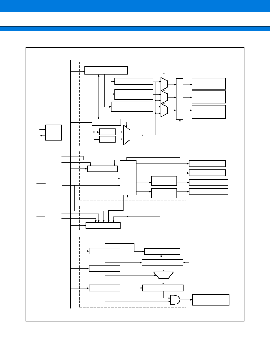
MB91340/MB91V340
97
∑
Block Diagram
X0
X1
PLL
1/2
R
|
B
U
S
DIVR0, 1 register
[Clock generator]
CPU clock division
Stop control
CPU clock
(CLKB)
Peripheral clock
(CLKP)
External bus
clock (CLKT)
Peripheral clock
division
External bus clock
division
CLKR register
Osc
illa-
tion
circu
it
[Stop/sleep
controller]
STCR register
Stop state
Internal interrupt
Internal reset
State
transi-
tion
con-
trol cir-
cuit
SLEEP state
Reset F/F
Reset F/F
Internal reset (RST)
Internal reset (INIT)
[Reset circuit]
RSRR register
WPR register
CTBR register
Watchdog F/F
TBCR register
Timebase counter
Overflow detection F/F
Interrupt enable
[Watchdog controller]
Timebase timer
interrupt request
Selec-
to
r
Selector
HST pin
RST pin
INIT pin
Selector
Count clock
Selec-
tor
Selec-
tor
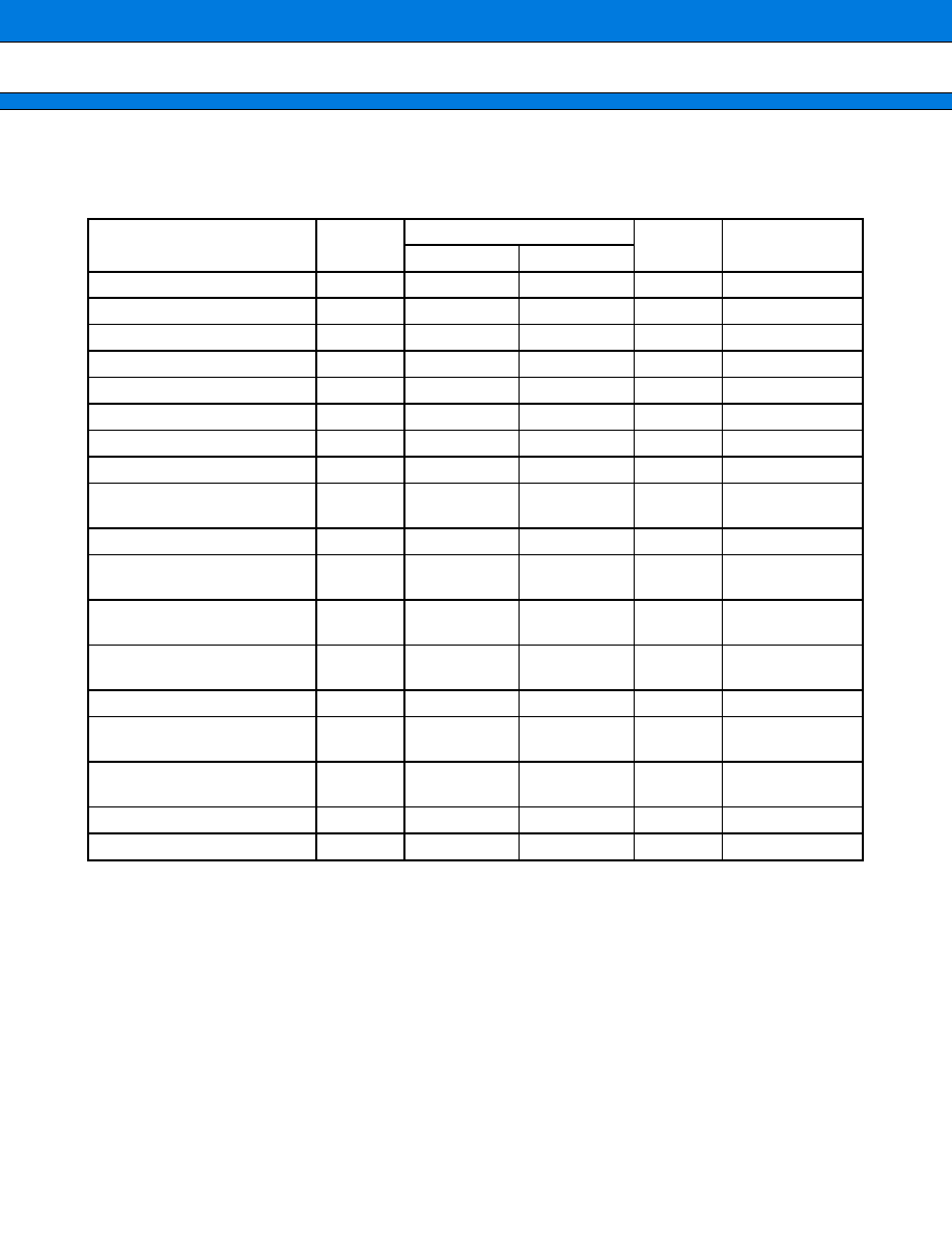
MB91340/MB91V340
98
s
ELECTRICAL CHARACTERISTICS
1.
Absolute Maximum Ratings
(V
SS
=
DAVS
=
AV
SS
=
0 V)
*1 : V
CC
3/V
CC
2 must not be lower than V
SS
-
0.5 V.
*2 : Ensure that the voltage does not exceed V
CC
3
+
0.3 V, including at power-on.
*3 : The maximum output current is the peak value for a single pin.
*4 : The average output current is the average current for a single pin over a period of 100ms.
*5 : The total average output current is the average current for all pins over a period of 100ms.
WARNING: Semiconductor devices can be permanently damaged by application of stress (voltage, current,
temperature, etc.) in excess of absolute maximum ratings. Do not exceed these ratings.
Parameter
Symbol
Rating
Unit
Remaeks
Min
Max
Supply voltage
V
CC
3
V
SS
-
0.5
V
SS
+
4.0
V
*1
Supply voltage
V
CC
2
V
SS
-
0.5
V
SS
+
3.0
V
*1
Analog supply voltage
DAVC
V
SS
-
0.5
V
SS
+
4.0
V
*2
Analog supply voltage
AV
CC
V
SS
-
0.5
V
SS
+
4.0
V
*2
Analog reference voltage
AVRH
V
SS
-
0.5
V
SS
+
4.0
V
*2
Input voltage
V
I
V
SS
-
0.3
V
CC
3
+
0.3
V
Analog pin input voltage
V
IA
V
SS
-
0.3
AV
CC
+
0.3
V
Output voltage
V
O
V
SS
-
0.3
V
CC
3
+
0.3
V
"L" level maximum output
current
I
OL
10
mA
*3
"L" level average output current
I
OLAV
8
mA
*4
"L" level total maximum output
current
I
OL
100
mA
"L" level total average output
current
I
OLAV
50
mA
*5
"H" level maximum output
current
I
OH
-
10
mA
*3
"H" level average output current
I
OHAV
-
4
mA
*4
"H" level total maximum output
current
I
OH
-
50
mA
"H" level total average output
current
I
OHAV
-
20
mA
*5
Power consumption
P
D
500
mW
Storage temperature
T
STG
-
50
+
125
∞
C
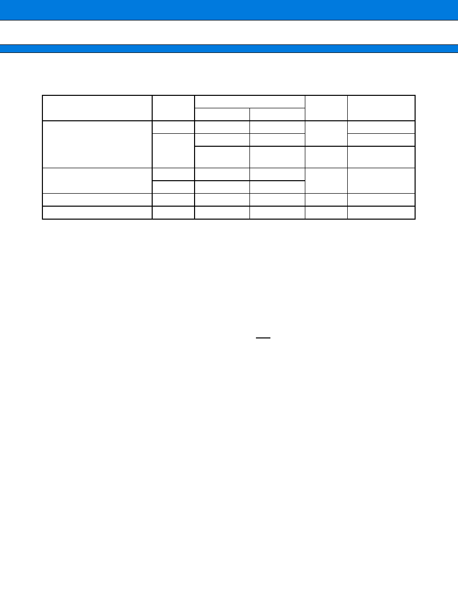
MB91340/MB91V340
99
2.
Recommended Operating Conditions
(V
SS
=
DAVS
=
AV
SS
=
0 V)
<Power-on precautions>
Although no particular restrictions apply to the sequence for turning the power on or off, the following sequence
is recommended.
Power-on : V
CC
2
V
CC
3
Pin signal inputs
Power-off : Pin signal inputs
V
CC
3
V
CC
2
Do not leave V
CC
3 connected for a long time period (e.g. 1 minute) while V
CC
2 is disconnected as this may
adversely affect the reliability of the LSI.
Due to electrical noise and similar, the state of internal circuits may not be maintained when V
CC
3 (external) is
restored from the OFF to the ON state. Always apply a reset (INIT) after power-on to initialize the LSI.
WARNING: The recommended operating conditions are required in order to ensure the normal operation of the
semiconductor device. All of the device's electrical characteristics are warranted when the device is
operated within these ranges.
Always use semiconductor devices within their recommended operating condition ranges. Operation
outside these ranges may adversely affect reliability and could result in device failure.
No warranty is made with respect to uses, operating conditions, or combinations not represented on
the data sheet. Users considering application outside the listed conditions are advised to contact their
FUJITSU representatives beforehand.
Parameter
Symbol
Value
Unit
Remarks
Min
Max
Supply voltage
V
CC
3
3.0
3.6
V
V
CC
2
2.3
2.7
Normal operation
2.3
2.7
V
Maintaining RAM
state in stop mode
Analog supply voltage
DAVC
V
SS
-
0.3
V
SS
+
3.6
V
AV
CC
V
SS
-
0.3
V
SS
+
3.6
Analog reference voltage
AVRH
AV
SS
AV
CC
V
Operating temperature
Ta
-
10
+
70
∞
C
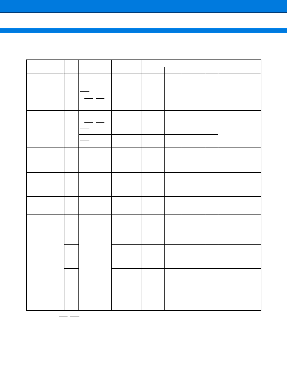
MB91340/MB91V340
100
3.
DC Characteristics
(V
CC
3
=
3.0 V to 3.6 V , V
CC
2
=
2.3 V to 2.7 V , V
SS
=
DAVS
=
AV
SS
=
0 V, Ta
=
-
10
∞
C to
+
70
∞
C)
*1 : Excludes X0, X1, pins with internal pull-down resistor (EX_BRQ, BREAK, ICD0 to ICD3), pins with internal pull-
up resistor (INIT, RST), and pins with a pull-up resistor set by PCR.
*2 : Values enclosed in brackets ( ) are for theMB91V340.
Parameter
Sym-
bol
Pin name
Condition
Value
Unit
Remarks
Min
Typ
Max
"H" level input
voltage
V
IH
Pins other
than X0, X1,
INIT, NMI,
HST, MD0 to 2
2.0
V
CC
3 + 0.3
V
INIT, NMI,
HST, MD0 to 2
0.8
◊
V
CC
3
V
CC
3 + 0.3
V
"L" level input
voltage
V
IL
Pins other
than X0, X1,
INIT, NMI,
HST, MD0 to 2
V
SS
0.8
V
INIT, NMI,
HST, MD0 to 2
V
SS
0.2
◊
V
CC
3
V
"H" level output
voltage
V
OH
All output pins
V
CC
3 = 3.0 V
I
OH
= -4.0 mA
V
CC
3 - 0.4
V
CC
3
V
"L" level output
voltage
V
OL
All output pins
V
CC
3 = 3.0 V
I
OL
= 4.0 mA
V
SS
0.4
V
Input leak
current
(Hi-Z output
leak current)
I
LI
All input pins*
1
V
CC
3 = 3.6 V
0.45 V
<
V
I
<
V
CC
3
-5
+5
µ
A
Pull-up
resistance
R
UP
RST, pins with
pull-up
settings
V
CC
3 = 3.6 V
V
I
= 0.45 V
10
25
120
k
Power supply
current*
2
I
CC
2
V
CC
2
f
C
= 16.5
MHz
V
CC
2 = 2.7 V
100
(150)
130
(200)
mA
When operating at :
CLKB:66 MHz
CLKP, CLKT :
33 MHz
(
◊
4 multiplier)
I
CCS
2
f
C
= 16.5
MHz
V
CC
2 = 2.7 V
60
(100)
80
(150)
mA
When operating at :
CLKP :
33 MHz
in sleep mode
I
CCH
2
Ta = 25
∞
C
V
CC
2 = 2.7 V
100
900
µ
A
In stop mode
Input
capacitance
C
IH
Other than
V
CC
3, V
CC
2,
V
SS
, AV
CC
,
AV
SS
, DAVC,
DAVS
10
pF
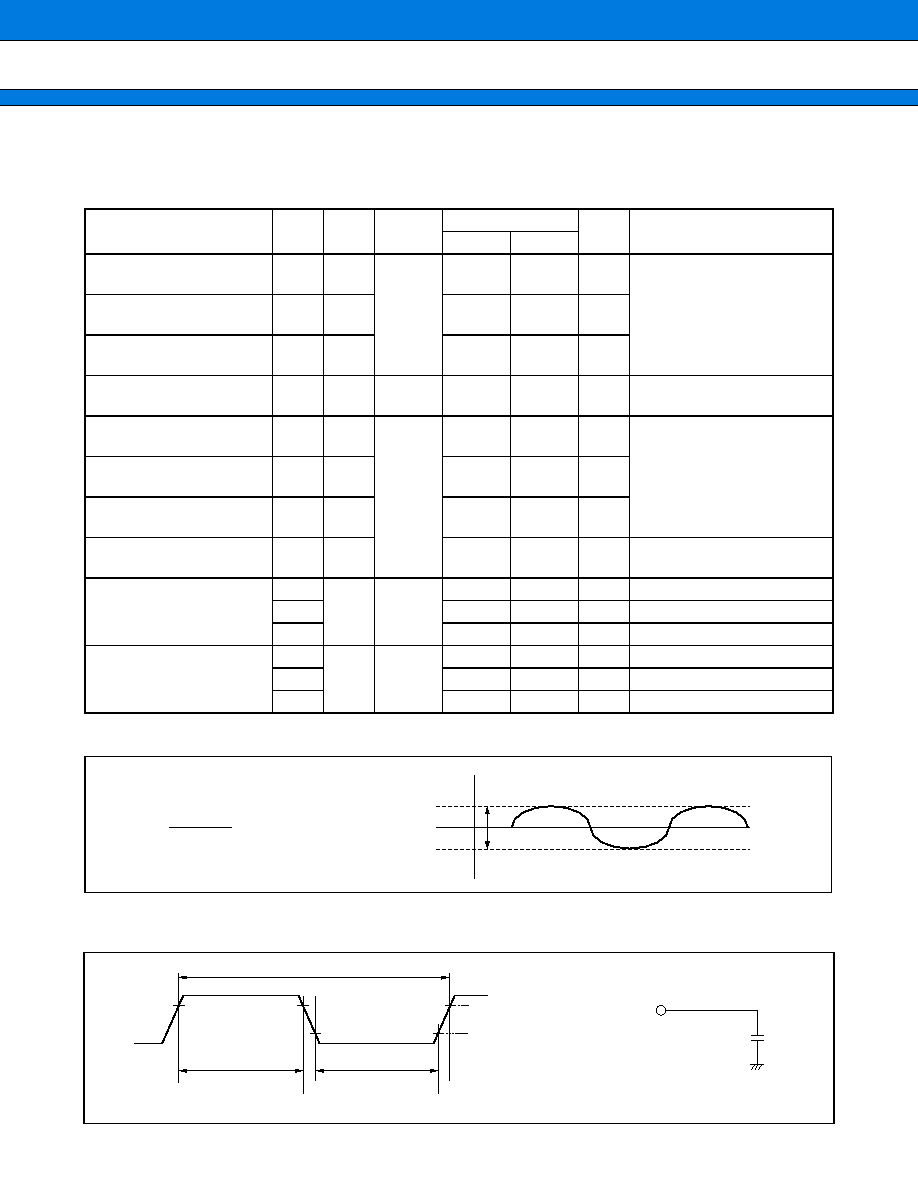
MB91340/MB91V340
101
4.
AC Characteristics
(1) Clock Timing Ratings
(V
CC
3
=
3.0 V to 3.6 V , V
CC
2
=
2.3 V to 2.7 V , V
SS
=
DAVS
=
AV
SS
=
0 V, Ta
=
-
10
∞
C to
+
70
∞
C)
*1 : The frequency fluctuation value is the maximum percentage deviation from the preset central frequency when
using the multiplier (when PLL is locked).
*2 : Values are for minimum clock frequency (12.5 MHz) input to X0, oscillation circuit uses PLL, and gear ratio
=
1/16.
∑
Conditions for measuring the clock timing ratings
Parameter
Sym-
bol
Pin
name
Condi-
tion
Value
Unit
Remarks
Min
Max
Clock frequency (1)
f
C
X0
X1
12.5
16.5
MHz
Using PLL
(When operating at max in-
ternal frequency (66 MHz)
=
16.5 MHz self-oscillation with
◊
4 PLL)
Clock cycle time
t
C
X0
X1
60.6
ns
Frequency fluctuation*
1
(PLL locked)
f
5
%
Clock frequency (2)
f
C
X0
X1
10
33
MHz
Self-oscillation (1/2 division
input)
Clock frequency (3)
f
C
X0
X1
10
33
MHz
External clock
Clock cycle time
t
C
X0
X1
40
100
ns
Input clock pulse width
P
WH
P
WL
X0
X1
16
ns
Input clock rise, fall time
t
CR
t
CF
X0
X1
8
ns
(t
CR
+
t
CF
)
Internal operation clock
frequency
f
CP
0.78*
2
66
MHz
CPU
f
CPP
0.78*
2
33
MHz
Peripherals
f
CPT
0.78*
2
33
MHz
External bus
Internal operation clock cy-
cle time
t
CP
15.2
1280*
2
ns
CPU
t
CPP
30.3
1280*
2
ns
Peripherals
t
CPT
30.3
1280*
2
ns
External bus
+
+
fo
fo
-
-
f
=
◊
100 (%)
Central
frequency
0.8 V
CC
3
0.2 V
CC
3
t
CF
t
CR
t
C
P
WH
P
WL
C
=
50 pF
Output pin
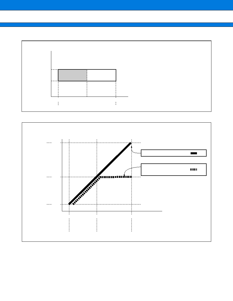
MB91340/MB91V340
102
∑
Warranted operation range
∑
External/internal clock setting range
*1 : If using the PLL, input an external clock in the range 12.5 MHz to 16.5 MHz.
*2 : Allow a PLL oscillation stabilization time of
>
300
µ
s.
*3 : Set the gear ratio for the internal clock to be within the values shown in the (1) Clock Timing Ratings table.
0
(MHz)
2.7
2.3
f
CP
/ f
CPP
66
33
0.78
V
CC
2 (V)
Internal clock
Power supply
Warranted operation range (Ta
=
-
10 to
+
70
∞
C)
f
CPP
is represented by the shaded area
66
(MHz)
33
16.5
4 : 4
2 : 2
1 : 2
f
CP
f
CPP
,
f
CPT
Internal clock
CPU : Peripheral
division ratio
CPU clock (CLKB) :
Peripheral clock (CLKP) ,
External bus clock (CLKT) :
Source oscillation input clock f
C
=
16.5 MHz
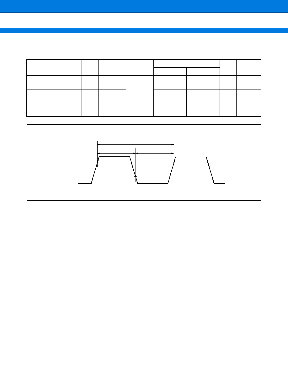
MB91340/MB91V340
103
(2) Clock Output Timing
(V
CC
3
=
3.0 V to 3.6 V , V
CC
2
=
2.3 V to 2.7 V , V
SS
=
DAVS
=
AV
SS
=
0 V, Ta
=
-
10
∞
C to
+
70
∞
C)
For the following AC ratings, the rating for HCLK are the same as for SYSCLK.
*1 : t
CYC
is the width of one clock cycle after gearing.
*2 : The following ratings are for the gear ratio set to
◊
1.
For the ratings when the gear ratio is set to between 1/2 and 1/16 , substitute 1/2 to 1/16 for n in the following
equation.
(1
/
2
◊
1
/
n)
◊
t
CYC
-
10
*3 : The following rating are for the gear ratio set to
◊
1.
Parameter
Sym-
bol
Pin name
Condition
Value
Unit
Remarks
Min
Max
Cycle time
t
CYC
MCLK
SYSCLK
t
CPT
ns
*1
MCLK
MCLK
SYSCLK
SYSCLK
t
CHCL
MCLK
SYSCLK
t
CYC
/
2
-
2.5
t
CYC
/
2
+
2.5
ns
*2
MCLK
MCLK
SYSCLK
SYSCLK
t
CLCL
MCLK
SYSCLK
t
CYC
/
2
-
2.5
t
CYC
/
2
+
2.5
ns
*3
MCLK
SYSCLK
V
OH
V
OL
V
OH
t
CYC
t
CLCH
t
CHCL
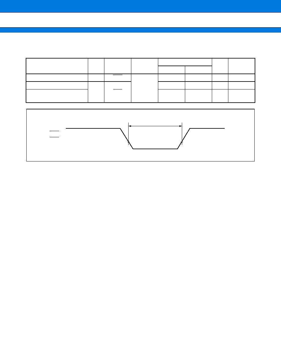
MB91340/MB91V340
104
(3) Reset and Hardware Standby Ratings
(V
CC
3
=
3.0 V to 3.6 V , V
CC
2
=
2.3 V to 2.7 V , V
SS
=
DAVS
=
AV
SS
=
0 V, Ta
=
-
10
∞
C to
+
70
∞
C)
Parameter
Sym-
bol
Pin name
Condition
Value
Unit
Remarks
Min
Max
Hardware standby input time
t
HSTL
HST
t
C
◊
10
ns
Init input time ( at power-on )
t
INTL
INIT
t
C
◊
2
23
ns
Init input time (other than at
power-on)
t
C
◊
10
ns
INIT
0.2 V
CC
3
tHSTL, tINTL
HST
MB91340/MB91V340
105
(4-1) Normal Bus Access Read/Write Operation
(V
CC
3
=
3.0 V to 3.6 V , V
CC
2
=
2.3 V to 2.7 V , V
SS
=
DAVS
=
AV
SS
=
0 V, Ta
=
-
10
∞
C to
+
70
∞
C)
Parameter
Sym-
bol
Pin name
Condition
Value
Unit
Remarks
Min
Max
CS0 to CS7 setup
t
CSLCH
MCLK
CS0 to CS7
AWRxL :
W02
=
0
3
ns
*3
t
CSDLCH
AWRxL :
W02
=
1
-
3
ns
*3
CS0 to CS7 hold
t
CHCSH
3
t
CYC
/
2
+
6
ns
Address setup
t
ASCH
MCLK
A23 to A00
3
ns
t
ASWL
WR0, WR1,
WR
A23 to A00
3
ns
t
ASRL
RD
A23 to A00
3
ns
Address hold
t
CHAX
MCLK
A23 to A00
3
t
CYC
/
2
+
6
ns
t
WHAX
WR0, WR1,
WR
A23 to A00
3
ns
t
RHAX
RD
A23 to A00
3
ns
Valid address
Valid data input time
t
AVDV
A23 to A00
D31 to D16
3
/
2
◊
t
CYC
-
11
ns
*1
*2
WR0, WR1, WR delay time
t
CHWL
MCLK
WR0, WR1,
WR
6
ns
WR0, WR1, WR delay time
t
CHWH
6
ns
WR0, WR1, WR minimum pulse
width
t
WLWH
WR0, WR1,
WR
12
ns
Data setup
WR0 to WR1, WR
t
DSWH
WR0, WR1,
WR
D31 to D16
t
CYC
ns
WR0, WR1, WR
Data hold time
t
WHDX
3
ns
RD delay time
t
CHRL
MCLK
RD
6
ns
RD delay time
t
CHRH
6
ns
RD
Valid data input time
t
RLDV
RD
D31 to D16
t
CYC
-
10
ns
*1
Data setup
RD
time
t
DSRH
10
ns
RD
Data hold time
t
RHDX
0
ns
RD minimum pulse width
t
RLRH
RD
12
ns
AS setup
t
ASLCH
MCLK
AS
3
ns
AS hold
t
CHASH
3
t
CYC
/
2
+
6
ns

MB91340/MB91V340
106
*1 : When the bus is delayed by automatic wait insertion or RDY input, add (t
CYC
◊
number of wait cycles) to the rated
values.
*2 : These rating are for the gear ratio set to
◊
1. For the ratings when the gear ratio is set to between 1/2 and
1/16, substitute 1/2 to 1/16
Equation : 3
/
(2n)
◊
t
CYC
-
11
*3 : AWRxL : Area Wait Register
MB91340/MB91V340
107
(4-2) Normal Bus Access Read/Write Operation
(V
CC
3
=
3.0 V to 3.6 V , V
CC
2
=
2.3 V to 2.7 V , V
SS
=
DAVS
=
AV
SS
=
0 V, Ta
=
-
10
∞
C to
+
70
∞
C)
Parameter
Sym-
bol
Pin name
Condition
Value
Unit
Remarks
Min
Max
BAA setup
t
BALCH
MCLK
BAA
3
ns
BAA hold
t
CHBAH
3
t
CYC
/
2
+
6
ns
UUB/ULBsetup
t
BLCH
MCLK
UUB/ULB
3
ns
UUB/ULB hold
t
CHBH
3
t
CYC
/
2
+
6
ns
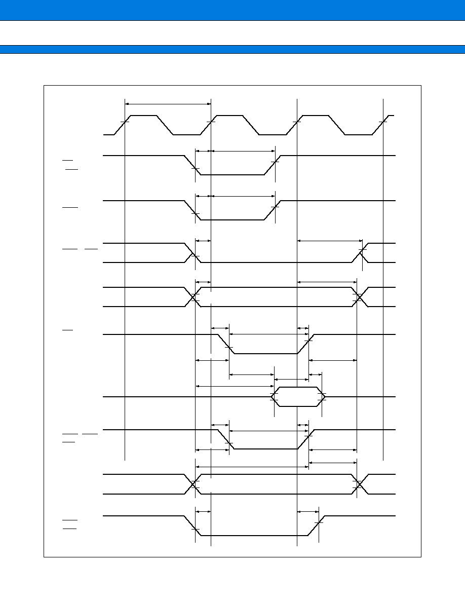
MB91340/MB91V340
108
MCLK
V
OH
V
OH
V
OL
V
IH
V
OH
V
IL
V
OL
V
OL
A23
A00
D31
D16
D31
D16
RD
CS0
CS7
BAA
V
OH
V
OH
V
OL
V
OH
V
OH
V
OH
V
OL
V
IH
V
IL
V
OH
V
OL
V
OH
t
ASCH
t
AVDV
t
RLDV
t
DSRH
t
RHDX
t
WLWH
t
CHWL
t
CHWH
t
CHAX
t
CHRH
t
DSWH
t
WHDX
t
CHBAH
t
CYC
t
BALCH
UUB
ULB
V
OL
V
OH
t
CHBH
t
BLCH
t
CHCSH
t
CHRL
t
RLRH
t
CSLCH
t
CSDLCH
AS
(LBA)
V
OL
V
OH
t
CHASH
t
ASLCH
BA1
t
ASRL
t
RHAX
t
ASWL
t
WHAX
WR0, WR1
WR
V
OH
V
OL
V
OH
V
OL
Write
Read
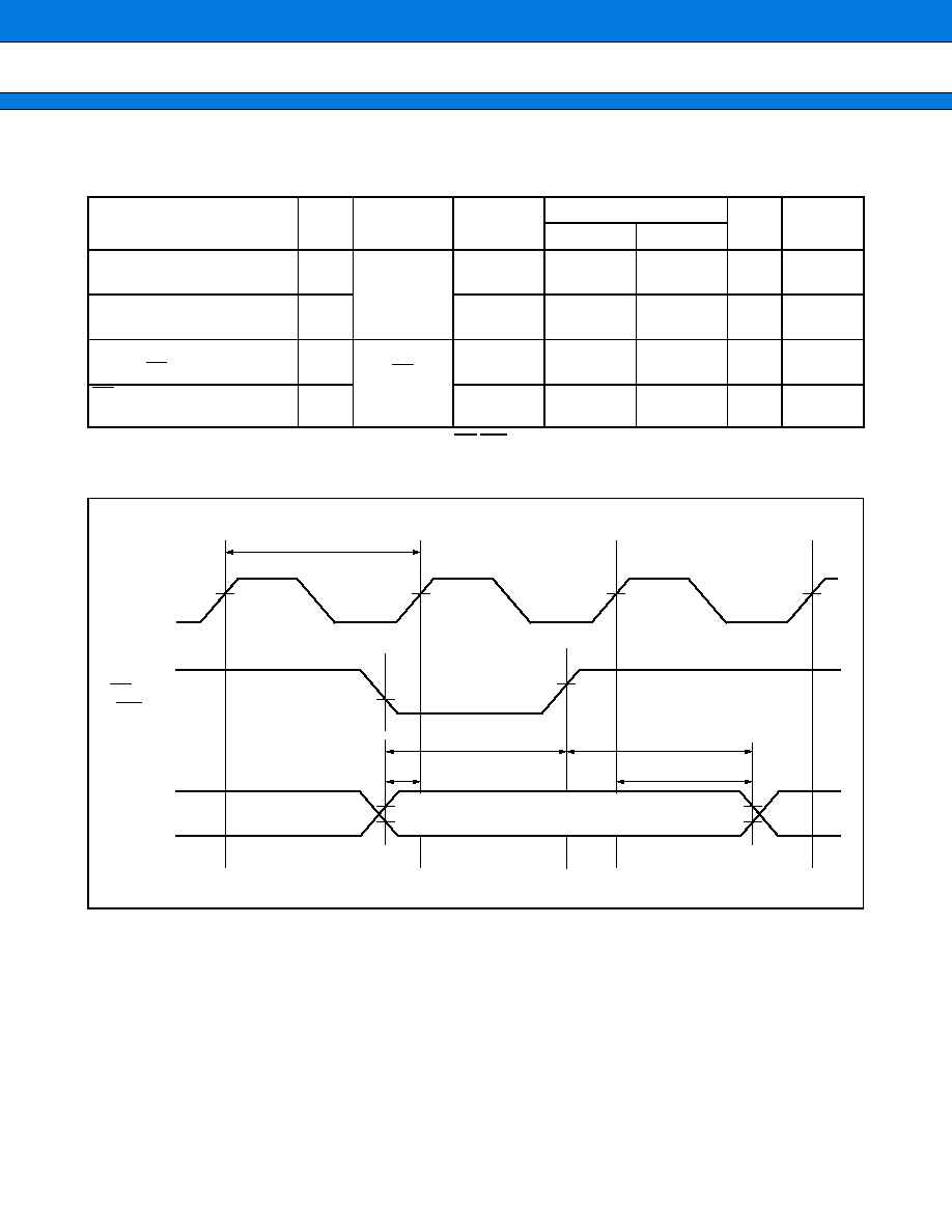
MB91340/MB91V340
109
(4-3) Multiplex Bus Access Read/Write Operation
(V
CC
3
=
3.0 V to 3.6 V , V
CC
2
=
2.3 V to 2.7 V , V
SS
=
DAVS
=
AV
SS
=
0 V, Ta
=
-
10
∞
C to
+
70
∞
C)
*1 : These ratings are not guaranteed when the CS
RD/WR Setup delay setting in AWR:bit1 is set to "0".
*2 : Ratings other than those shown above are the same as for the normal bus interface.
Parameter
Sym-
bol
Pin name
Condition
Value
Unit
Remarks
Min
Max
D31 to D16 address setup
time
MCLK
t
ASCH
MCLK
D31 to D16
3
ns
MCLK
D31 to D16 address hold time
t
CHAX
3
t
CYC
/
2
+
6
ns
D31 to D16 address setup
time
AS
t
ASASH
AS
D31 to D16
12
ns
AS
D31 to D16
address hold time
t
ASHAX
t
CYC
-
3
t
CYC
+
3
ns
MCLK
V
OH
V
OL
D31
D16
V
OH
V
OH
V
OH
V
OH
V
OL
V
OH
t
ASCH
t
CHAX
t
ASASH
t
ASHAX
t
CYC
AS
(LBA)
V
OL
V
OH
BA1
Address

MB91340/MB91V340
110
(5) Ready Input Timings
(V
CC
3
=
3.0 V to 3.6 V , V
CC
2
=
2.3 V to 2.7 V , V
SS
=
DAVS
=
AV
SS
=
0 V, Ta
=
-
10
∞
C to
+
70
∞
C)
Parameter
Sym-
bol
Pin name
Condition
Value
Unit
Remarks
Min
Max
RDY setup time
MCLK
t
RDYS
MCLK
RDY
10
ns
MCLK
RDY hold time
t
RDYH
MCLK
RDY
0
ns
MCLK
V
OH
V
OH
V
OL
V
OL
V
IL
V
IH
V
IL
V
IH
V
IH
V
IL
V
IH
V
IL
t
RDYH
t
RDYH
RDY
RDY
t
CYC
t
RDYS
t
RDYS
(Wait specified
by RDY)
(No wait specified
by RDY)
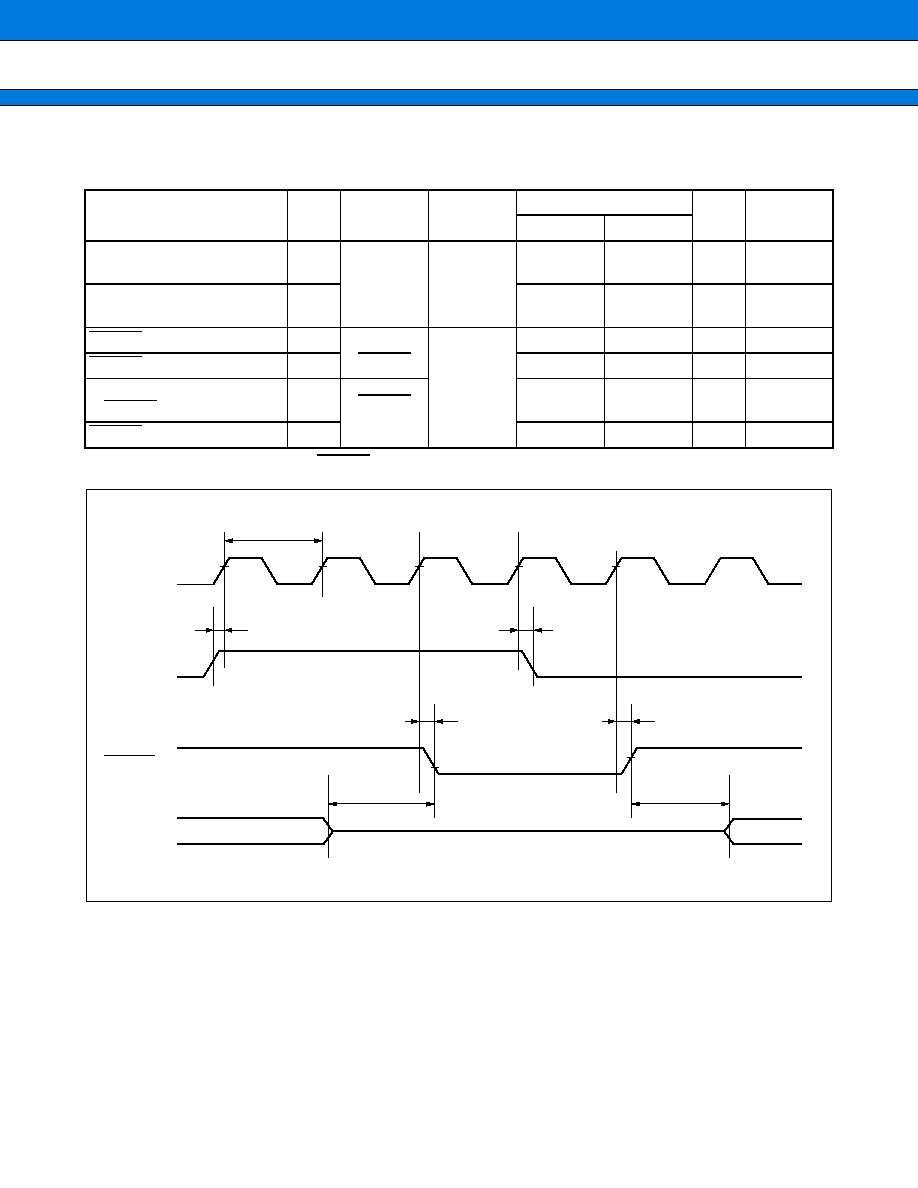
MB91340/MB91V340
111
(6) Hold Timing
(V
CC
3
=
3.0 V to 3.6 V , V
CC
2
=
2.3 V to 2.7 V , V
SS
=
DAVS
=
AV
SS
=
0 V, Ta
=
-
10
∞
C to
+
70
∞
C)
* : The time from receiving BRQ to BGRNT changing is one cycle or more.
Parameter
Sym-
bol
Pin name
Condition
Value
Unit
Remarks
Min
Max
BRQ setup time
MCLK
t
BRQS
MCLK
BRQ
10
ns
MCLK
BRQ hold time
t
BRQH
0
ns
BGRNT delay time
t
CHBGL
MCLK
BGRNT
t
CYC
/
2
-
6
t
CYC
/
2
+
6
ns
BGRNT delay time
t
CHBGH
t
CYC
/
2
-
6
t
CYC
/
2
+
6
ns
Pin floating
BGRNT
time
t
XZBGL
BGRNT
Other pins
t
CYC
-
10
t
CYC
+
10
ns
BGRNT
Pin valid time
t
BGHXV
t
CYC
-
10
t
CYC
+
10
ns
MCLK
V
OH
t
CHBGL
V
OL
V
OH
V
IH
V
IL
V
OH
V
OH
V
OH
t
CHBGH
BRQ
BGRNT
t
CYC
t
BGHXV
t
XZBGL
t
BRQS
t
BRQH
Other pins
High-Z
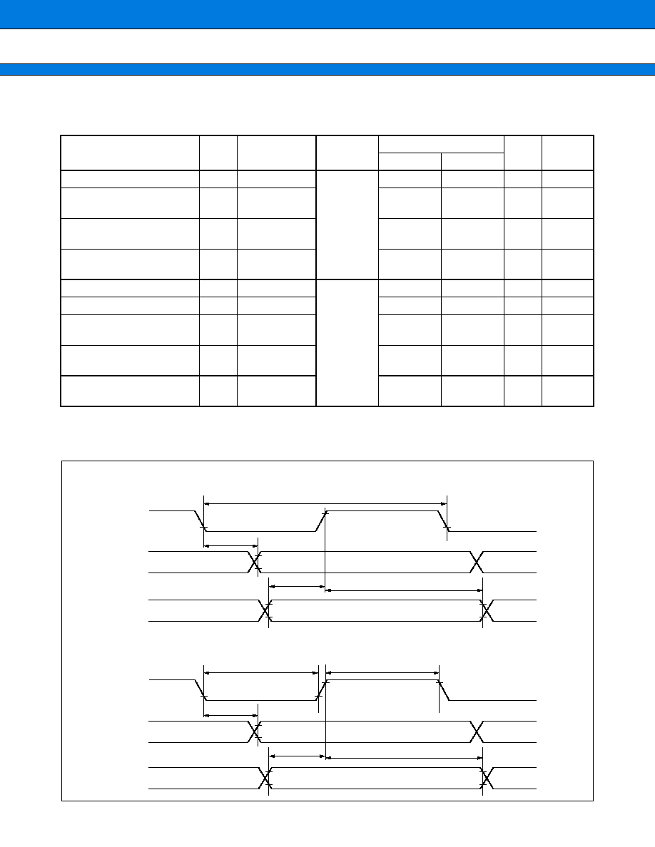
MB91340/MB91V340
112
(7) UART Timing
(V
CC
3
=
3.0 V to 3.6 V , V
CC
2
=
2.3 V to 2.7 V , V
SS
=
DAVS
=
AV
SS
=
0 V, Ta
=
-
10
∞
C to
+
70
∞
C)
*1 : These are the AC ratings for CLK synchronous mode.
*2 : t
CYCP
is the peripheral clock cycle time.
Parameter
Sym-
bol
Pin name
Condition
Value
Unit
Remarks
Min
Max
Serial clock cycle time
t
SCYC
SCK0 to SCK2
Internal
shift clock
mode
8 t
CYCP
ns
SCK
SO delay time
t
SLOV
SCK0 to SCK2
SO0 to SO2
-
80
80
ns
Valid SI
SCK
t
IVSH
SCK0 to SCK2
SI0 to SI2
100
ns
SCK
valid SI hold time
t
SHIX
SCK0 to SCK2
SI0 to SI2
60
ns
Serial clock "H" pulse width
t
SHSL
SCK0 to SCK2
External
shift clock
mode
4 t
CYCP
ns
Serial clock "L" pulse width
t
SLSH
SCK0 to SCK2
4 t
CYCP
ns
SCK
SO delay time
t
SLOV
SCK0 to SCK2
SO0 to SO2
150
ns
Valid SI
SCK
t
IVSH
SCK0 to SCK2
SI0 to SI2
60
ns
SCK
valid SI hold time
t
SHIX
SCK0 to SCK2
SI0 to SI2
60
ns
∑
Internal shift clock mode
∑
External shift clock mode
SCK0 to SCK2
SO0 to SO2
SI0 to SI2
t
SCYC
t
SLOV
t
IVSH
t
SHIX
V
OL
V
OH
V
OL
V
OH
V
OL
V
IH
V
IL
V
IH
V
IL
SCK0 to SCK2
SO0 to SO2
SI0 to SI2
t
SLOV
t
SLSH
t
SHSL
t
IVSH
t
SHIX
V
OH
V
OL
V
IH
V
IH
V
IL
V
IL
V
IH
V
IL
V
IH
V
IL
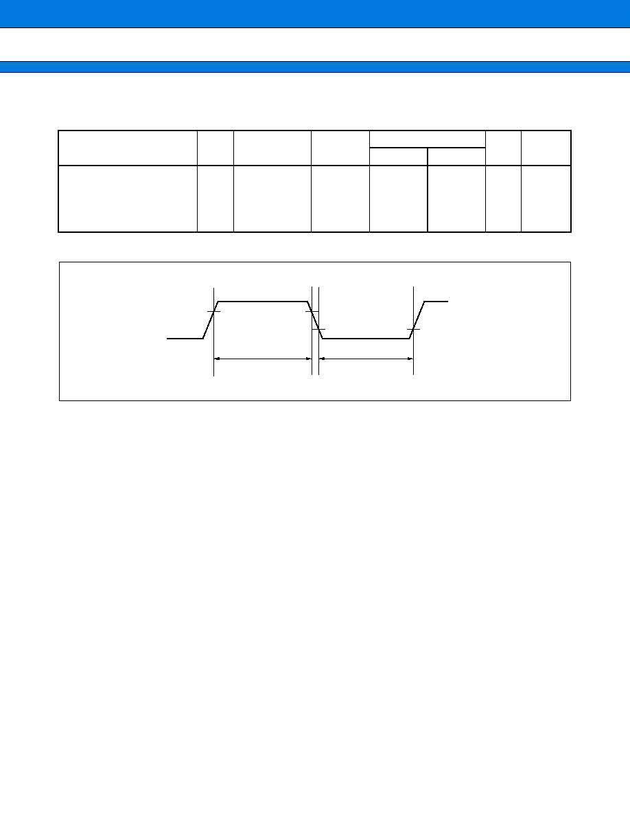
MB91340/MB91V340
113
(8) Freerun Timer Clock, Reload Timer Clock, and PPG Timer Input Timings
(V
CC
3
=
3.0 V to 3.6 V , V
CC
2
=
2.3 V to 2.7 V , V
SS
=
DAVS
=
AV
SS
=
0 V, Ta
=
-
10
∞
C to
+
70
∞
C)
* : t
CYCP
is the peripheral clock cycle time.
Parameter
Sym-
bol
Pin name
Condition
Value
Unit
Remarks
Min
Max
Input pulse width
t
TIWH
t
TIWL
FRCK
TIN0 to TIN3
AIN0 to AIN3
BIN0 to BIN3
ZIN0 to ZIN3
2 t
CYCP
*
ns
t
TIWH
t
TIWL
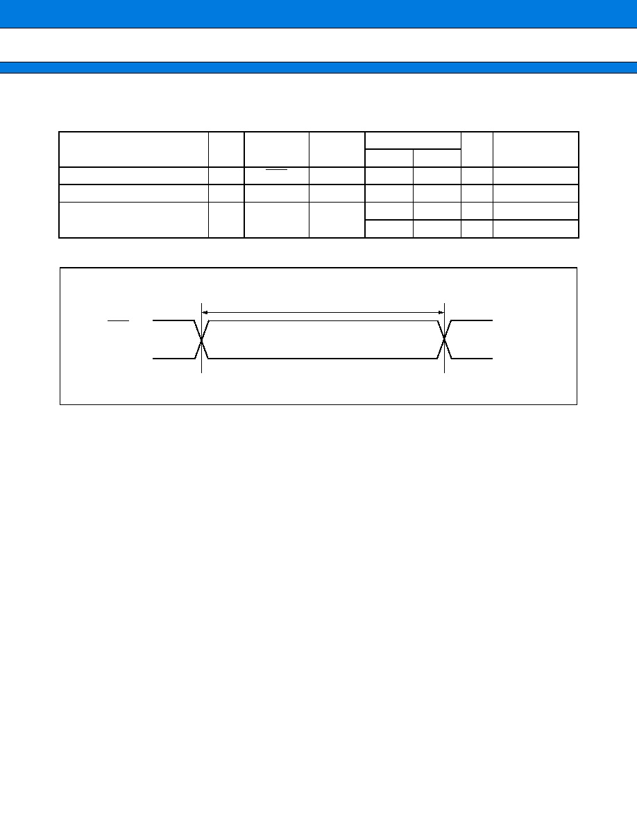
MB91340/MB91V340
114
(9) Trigger Input Timing
(V
CC
3
=
3.0 V to 3.6 V , V
CC
2
=
2.3 V to 2.7 V , V
SS
=
DAVS
=
AV
SS
=
0 V, Ta
=
-
10
∞
C to
+
70
∞
C)
* : t
CYCP
is the peripheral clock cycle time.
Parameter
Sym-
bol
Pin name
Condition
Value
Unit
Remarks
Min
Max
A/D activation trigger input time
t
ATGX
ATG
5 t
CYCP
*
ns
Input capture input trigger
t
INP
IN0 to IN3
5 t
CYCP
*
ns
External interrupt input
pulse width
t
TRGH
t
TRGL
INT0 to INT7
3 t
CYCP
*
ns
Normal operation
1
µ
s
In stop mode
t
ATGX
, t
INP
,
t
TRGH
, t
TRGL
ATG
IN0
IN3
INT0
INT7
MB91340/MB91V340
115
(10) DMA Controller Timing
(V
CC
3
=
3.0 V to 3.6 V , V
CC
2
=
2.3 V to 2.7 V , V
SS
=
DAVS
=
AV
SS
=
0 V, Ta
=
-
10
∞
C to
+
70
∞
C)
[ For edge detection ] (Block/step transfer mode, burst transfer mode)
* : When f
CPT
>
f
CP
, t
CYC
becomes same as t
CP
.
[ For level detection ] (Demand transfer mode)
[ For all operation modes ]
(Continued)
Parameter
Sym-
bol
Pin name
Condition
Value
Unit
Remarks
Min
Max
DREQ input pulse width
t
DRWL
DREQ0 to DREQ2
2 t
CYC
*
ns
DSTP input pulse width
t
DSWH
DSTP0 to DSTP2
2 t
CYC
*
ns
Parameter
Sym-
bol
Pin name
Condition
Value
Unit
Remarks
Min
Max
DREQ setup time
t
DRS
MCLK
DREQ0 to DREQ2
10
ns
DREQ hold time
t
DRH
MCLK
DREQ0 to DREQ2
0
ns
DSTP setup time
t
DSTPS
MCLK
DSTP0 to DSTP2
10
ns
DSTP hold time
t
DSTPH
MCLK
DSTP0 to DSTP2
0
ns
Parameter
Sym-
bol
Pin name
Condition
Value
Unit
Remarks
Min
Max
DACK delay time
t
DALCH
MCLK
DACK0 to DACK2
AWRxL* :
W02
=
0
3
ns
CS timing
6
ns
FR30 compatible
t
DADLCH
AWRxL :
W02
=
1
-
3
ns
CS timing
6
ns
FR30 compatible
t
CHDAH
t
CYC
/
2
+
6
ns
CS timing
6
ns
FR30 compatible
DEOP delay
time
t
DELCH
MCLK
DEOP0 to DEOP2
AWRxL :
W02
=
0
3
ns
CS timing
6
ns
FR30 compatible
t
DEDLCH
AWRxL :
W02
=
1
-
3
ns
CS timing
6
ns
FR30 compatible
t
CHDEH
t
CYC
/
2
+
6
ns
CS timing
6
ns
FR30 compatible
MB91340/MB91V340
116
(Continued)
* : AWRxL : Area Wait Register
Parameter
Sym-
bol
Pin name
Condition
Value
Unit
Remarks
Min
Max
IORD delay time
t
CHIRL
MCLK
IORD
6
ns
t
CHIRH
6
ns
IOWR delay time
t
CHIWL
MCLK
IOWR
6
ns
t
CHIWH
6
ns
IORD minimum
pulse width
t
IRLIRH
IORD
12
ns
IOWR minimum
pulse width
t
IWLIWH
IOWR
12
ns
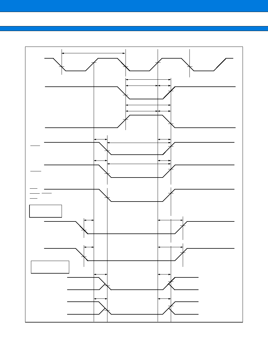
MB91340/MB91V340
117
MCLK
DACK0
DACK2
DACK0
DACK2
DREQ0
DREQ2
DSTP0
DSTP2
IORD
V
OL
V
OH
V
OL
V
OL
V
OH
V
OL
V
OH
V
OL
V
OH
V
OL
V
OH
V
OL
V
OH
V
OL
V
OH
V
IL
V
IH
V
IL
V
IH
t
DALCH
t
DADLCH
t
CHIRL
t
CHIWL
t
IRLIRH
t
IWLIWH
t
DALCH
t
DADLCH
t
CYC
t
CHIRH
t
CHIWH
t
DRS
t
DRH
t
DSTPS
t
DSTPH
t
DRWL
t
DSWH
t
CHDAH
DEOP0
DEOP2
V
OL
V
OH
t
DELCH
t
DEDLCH
t
CHDEH
IOWR
RD
WR0
,
WR1
WR
DEOP0
DEOP2
V
OL
V
OH
t
DELCH
t
DEDLCH
t
CHDAH
t
CHDEH
Chip select
timing
FR30
compatible timing
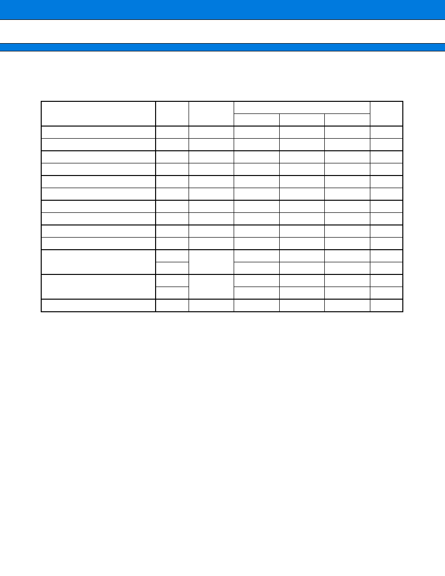
MB91340/MB91V340
118
5.
Electrical Characteristics for the A/D Converter
(V
CC
3
=
AV
CC
=
3.0 V to 3.6 V , V
CC
2
=
2.3 V to 2.7 V , V
SS
=
DAVS
=
AV
SS
=
0 V,
AVRH
=
3.0 V to 3.6 V , Ta
=
-
10
∞
C to
+
70
∞
C)
*1 : For V
CC
3
=
AV
CC
=
3.0 V to 3.6 V , machine clock
=
33 MHz
*2 : Current when A/D converter not operating and CPU in stop mode (V
CC
3
=
AV
CC
=
AVRH
=
3.6 V)
Notes :
∑
The relative error increases as AVRH becomes smaller.
∑
Ensure that the output impedance of the external circuit connected to the analog input meets the following
condition :
Output impedance of external circuit
<
4 k
If the output impedance of the external circuit is too high, the analog voltage sampling time may be too
short.
Parameter
Symbol
Pin name
Value
Unit
Min
Typ
Max
Resolution
10
10
BIT
Total error
-
8.5
8.5
LSB
Linearity error
-
3.0
3.0
LSB
Differential linearity error
-
2.5
2.5
LSB
Zero transition error
V
OT
AN0 to AN7
-
8.0
0.5
8.0
LSB
Full-scale transition error
V
FST
AN0 to AN7
AVRH
-
8.0
AVRH
-
1.5
AVRH
+
8.0
LSB
Conversion time*
1
5.4
µ
s
Analog port input current
I
AIN
AN0 to AN7
0.1
10
µ
A
Analog input voltage
V
AIN
AN0 to AN7
AVss
AVRH
V
Reference voltage
AVRH
AVss
AV
CC
V
Power supply current
I
A
AV
CC
0.6
2
mA
I
AH
*
2
10
µ
A
Reference voltage supply current
I
R
AVRH
0.6
2
mA
I
RH
*
2
10
µ
A
Variation between channels
AN0 to AN7
5
LSB

MB91340/MB91V340
119
∑
Definition of A/D Converter Terms
∑
Resolution
: The change in analog voltage that can be recognized by the A/D converter.
∑
Linearity error : The deviation between the actual conversion characteristics and the line linking the zero
transition point (00 0000 0000
00 0000 0001) and the full scale transition point (11 1111
1110
11 1111 1111) .
∑
Differential
linearity error
: The variation from the ideal input voltage required to change the output code by 1 LSB.
∑
Total error
: The total error is the difference between the actual value and the theoretical value. Includes
the zero transition error, full-scale transition error and linearity error.
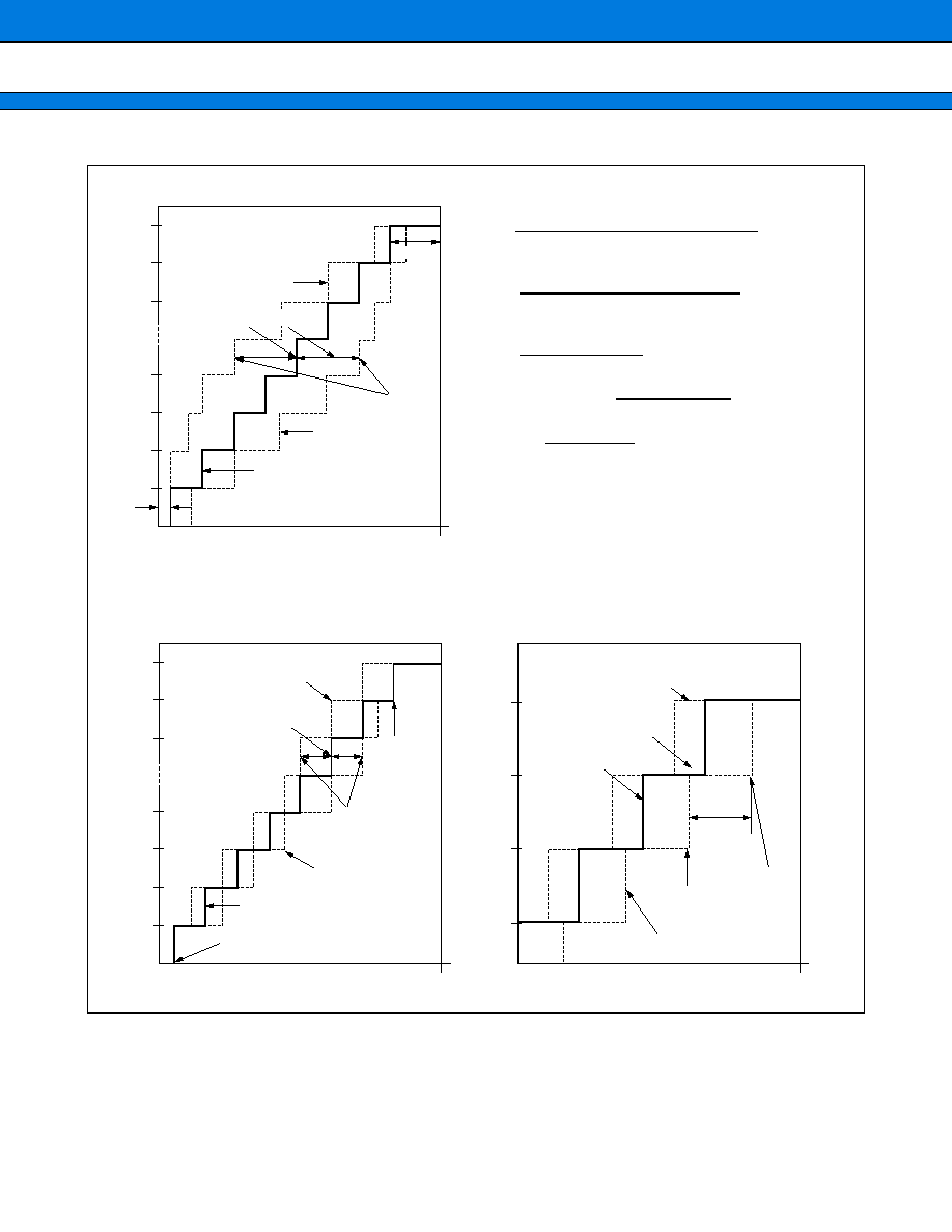
MB91340/MB91V340
120
3FF
3FE
3FD
004
003
002
001
AV
SS
AVRH
1.5 LSB'
V
NT
0.5 LSB'
{1 LSB
◊
(N
-
1)
+
0.5 LSB}
Total Error
Digital Output
Actual conversion
characteristic
(Measured value)
Actual conversion
characteristic
Theoretical
characteristic
Analog Input
Total error for digital output N
=
V
NT
-
{1 LSB'
◊
(N
-
1)
+
0.5 LSB'}
1 LSB'
[V]
V
OT
' (Theoretical value)
=
AV
SS
+
0.5 LSB' [V]
V
FST
' (Theoretical value)
=
AVRH
-
1.5 LSB' [V]
V
NT
: Voltage at which digital output changes from (N
+
1)
to N.
Linearity error for digital output N
=
V
NT
-
{1 LSB
◊
(N
-
1)
+
V
OT
}
1 LSB
[LSB]
Differential linearity error for digital output N
=
V (
N
+
1
)
T
-
V
NT
1 LSB
-
1
1 LSB
=
V
FST
-
V
OT
1022
[V]
1 LSB'
(Theoretical value)
AVRH
-
AV
SS
1024
[V]
V
OT
: Voltage at which digital output changes from
(000)
H
to (001)
H
.
[LSB]
3FF
3FE
3FD
004
003
002
001
AV
SS
AVRH
{1 LSB
◊
(N
-
1)
+
V
OT
'}
V
NT
V
FST
V
OT
N
-
1
AV
SS
AVRH
N
-
2
N
N
+
1
V
NT
V
FST
Linearity Error
Differential Linearity Error
Digital Output
Digital Output
Actual conversion
characteristic
(Measured
value)
Actual conversion
characteristic
Theoretical characteristic
(Measured value)
Analog Input
Analog Input
Theoretical
characteristic
Actual conversion
characteristic
(Measured
value)
(Measured
value)
Actual conversion characteristic
=
(Measured value)
MB91340/MB91V340
121
6.
Electrical Characteristics for the D/A Converter
(V
CC
3
=
DAVC
=
3.0 V to 3.6 V , V
CC
2
=
2.3 V to 2.7 V , V
SS
=
DAVS
=
AV
SS
=
0 V,
AVRH
=
3.0 V to 3.6 V , Ta
=
-
10
∞
C to
+
70
∞
C)
*1 : No output occurs in the range DAVS to DAVS + 100 mV and DAVC to DAVC - 100 mV.
*2 : Current when D/A converter not operating and CPU in stop mode (V
CC
3
=
DAVC
=
3.6 V) .
Example Output Linearity Table
(V
CC
3
=
DAVC
=
3.0 V , V
CC
2
=
2.3 V to 2.7 V , V
SS
=
DAVS
=
AV
SS
=
0 V, AVRH
=
3.0 V , Ta
=
-
10
∞
C to
+
70
∞
C)
Parameter
Symbol
Pin name
Value
Unit
Min
Typ
Max
Resolution
8
BIT
DA output guaranteed range for
linearity error and differential
linearity error
V
OUT
*
1
DA0 to DA2 DAVS
+
0.25
DAVC
-
0.25
V
Linearity error
-
2
0
2
LSB
Differential linearity error
-
0.7
0
0.7
LSB
Conversion time
DA0 to DA2
5
µ
s
Output offset
V
OFF
DA0 to DA2
-
50
0
50
mV
Load
Capaci-
tance
C
L
DA0 to DA2
20
pF
Current
I
L
DA0 to DA2
-
250
250
µ
A
Power supply current
I
DA
DAVC
0.35
1
2
mA
I
DAH
*
2
10
µ
A
Digital Value
Output voltage (V)
Hex.
Dec.
D7
D6
D5
D4
D3
D2
D1
D0
FF
255
1
1
1
1
1
1
1
1
Outside guaranteed range for
linearity error and differential
linearity error
(relative size is guaranteed)
~
~
~
~
~
~
~
~
~
~
EB
235
1
1
1
0
1
0
1
1
EA
234
1
1
1
0
1
0
1
0
2.742
E9
233
1
1
1
0
1
0
0
1
2.730
~
~
~
~
~
~
~
~
~
~
~
17
23
0
0
0
1
0
1
1
1
0.270
16
22
0
0
0
1
0
1
1
0
0.258
15
21
0
0
0
1
0
1
0
1
Outside guaranteed range for
linearity error and differential
linearity error
(relative size is guaranteed)
~
~
~
~
~
~
~
~
~
~
00
0
0
0
0
0
0
0
0
0
D/A output voltage
=
(DAVC
-
DAVS)
◊
(digital value (dec.))
+
DAVS
256
[V]
MB91340/MB91V340
122
s
EXAMPLE CHARACTERISTICS
Power supply current example characterictics
160
140
120
100
80
60
40
20
0
2.3
2.5
V
CC
2 (V)
I
CC
2 (mA)
2.7
100
80
60
40
20
0
2.3
2.5
V
CC
2 (V)
I
CCS
2 (mA)
2.7
2.5
2
1.5
1
0.5
0
3
3.3
AV
CC
(V)
I
A
(mA)
3.6
2.5
2
1.5
1
0.5
0
3
3.3
AVRH (V)
I
R
(mA)
3.6
2.5
2
1.5
1
0.5
0
3
3.3
DAVC (V)
I
DA
(mA)
3.6
100000
10000
1000
3
3.3
V
CC
3 (V)
R (pull-up) (
)
3.6
I
CC
2
-
V
CC
2
(Ta
=
+
25
∞
C, CLKB
=
66 MHz)
I
CCS
2
-
V
CC
2
(Ta
=
+
25
∞
C, CLKP
=
33 MHz)
I
A
-
AV
CC
(Ta
=
+
25
∞
C, CLKP
=
33 MHz)
I
R
-
AVRH
(Ta
=
+
25
∞
C, CLKP
=
33 MHz)
I
DA
-
DAVC
(Ta
=
+
25
∞
C, CLKP
=
33 MHz)
R (pull-up)
-
V
CC
3
(Ta
=
+
25
∞
C)
MB91340/MB91V340
123
s
ORDERING IMFORMATION
Part No.
Package
Remarks
MB91340PMT
176-pin Plastic LQFP
(FPT-176P-M02)
MB91V340CR
361-pin Ceramic PGA
(PGA-361C-A01)
MB91340/MB91V340
124
s
PACKAGE DIMENSIONS
(Continued)
361-pin Ceramic PGA
(PGA-361C-A01)
Dimensions in mm (inches)
45.72 ± 0.53
(1.800 ± .021)
SQ
INDEX AREA
1994 FUJITSU LIMITED R361002SC-2-2
2.54 (.100) TYP
0.40 ± 0.10
(.016 ± .004)
DIA
43.18 (1.700)
REF
1.20 ± 0.25
(.047 ± .010)
5.27 (.207)
MAX
3.40 ± 0.40
(.134 ± .016)
1.00 (.039) DIA TYP
(4 PLCS)
EXTRA INDEX PIN
1.02 (.040) C TYP
(4 PLCS)
C
MB91340/MB91V340
125
(Continued)
176-pin Plastic LQFP
(FPT-176P-M02)
*Pins width and pins thickness include plating thickness.
Dimensions in mm (inches)
C
2000 FUJITSU LIMITED F176006S-c-2-4
Details of "A" part
0∞~8∞
0.50±0.20
(.020±.008)
0.60±0.15
(.024±.006)
0.25(.010)
(Stand off)
(.004±.004)
0.10±0.10
1.50
+0.20
≠0.10
+.008
≠.004
.059
(Mounting height)
0.08(.003)
(.006±.002)
0.145±0.055
"A"
INDEX
1
LEAD No.
44
45
88
89
132
133
176
0.50(.020)
0.22±0.05
(.009±.002)
M
0.08(.003)
24.00±0.10(.945±.004)SQ
26.00±0.20(1.024±.008)SQ

MB91340/MB91V340
FUJITSU LIMITED
All Rights Reserved.
The contents of this document are subject to change without notice.
Customers are advised to consult with FUJITSU sales
representatives before ordering.
The information and circuit diagrams in this document are
presented as examples of semiconductor device applications, and
are not intended to be incorporated in devices for actual use. Also,
FUJITSU is unable to assume responsibility for infringement of
any patent rights or other rights of third parties arising from the use
of this information or circuit diagrams.
The products described in this document are designed, developed
and manufactured as contemplated for general use, including
without limitation, ordinary industrial use, general office use,
personal use, and household use, but are not designed, developed
and manufactured as contemplated (1) for use accompanying fatal
risks or dangers that, unless extremely high safety is secured, could
have a serious effect to the public, and could lead directly to death,
personal injury, severe physical damage or other loss (i.e., nuclear
reaction control in nuclear facility, aircraft flight control, air traffic
control, mass transport control, medical life support system, missile
launch control in weapon system), or (2) for use requiring
extremely high reliability (i.e., submersible repeater and artificial
satellite).
Please note that Fujitsu will not be liable against you and/or any
third party for any claims or damages arising in connection with
above-mentioned uses of the products.
Any semiconductor devices have an inherent chance of failure. You
must protect against injury, damage or loss from such failures by
incorporating safety design measures into your facility and
equipment such as redundancy, fire protection, and prevention of
over-current levels and other abnormal operating conditions.
If any products described in this document represent goods or
technologies subject to certain restrictions on export under the
Foreign Exchange and Foreign Trade Law of Japan, the prior
authorization by Japanese government will be required for export
of those products from Japan.
F0203
©
FUJITSU LIMITED Printed in Japan