DS07-16308-1E
FUJITSU SEMICONDUCTOR
DATA SHEET
32-Bit RISC Microcontroller
CMOS
FR30 Series
MB91133/MB91F133
s
DESCRIPTION
The MB91133/MB91F133, a standard single-chip microcontroller featuring various I/O resources and bus control
mechanisms to incorporate the control required for high-performance high-speed CPU processes, is the core unit
in the 32-bit RISC CPU (FR family) .
This unit has the optimal specifications for incorporating applications that require high-performance CPU pro-
cessing power by featuring peripheral I/O resources suitable for single-lens reflex cameras, digital video cameras,
etc.
s
FEATURES
1.
CPU
∑ 32-bit RISC (FR30) , load/store architecture, 5-level pipeline
∑ Multi-purpose register : 32 bits
◊
16
∑ 16-bit fixed length instructions (basic instructions) , 1 instruction per cycle
∑ Instructions for barrel shift, bit processing and inter-memory transfers : Instructions suited to loading purposes
∑ Function entry / exit instruction, multi load / store instruction of register details : High-level language handling
instruction
∑ Register interlock function : Simplification of assembler description
∑ Branch instruction with delay slot : Reduction in overheads in case of branching
∑ Multiplier is built-in / supported at instruction level.
∑ Signed 32-bit multiplication : 5 cycles
∑ Signed 16-bit multiplication : 3 cycles
∑ Interruption (saving PC and PS) : 6 cycles, 16 priority levels
(Continued)
s
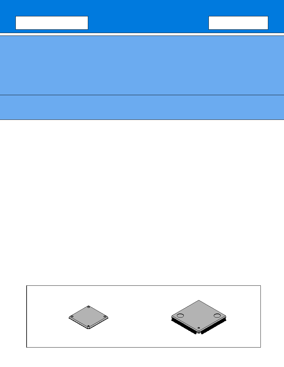
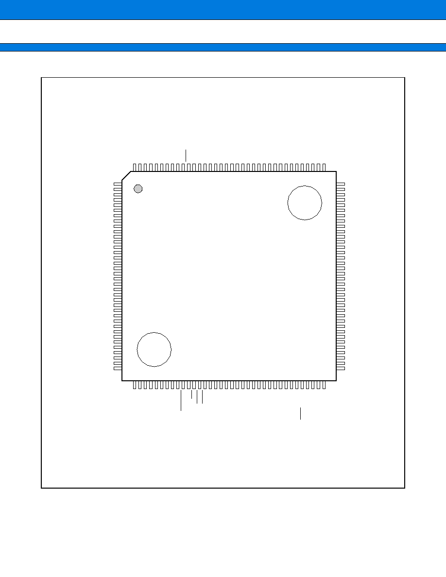
PACKAGES
144-pin plastic FBGA
144-pin plastic LQFP
(BGA-144P-M01)
(FPT-144P-M08)

MB91133/MB91F133
2
(Continued)
2.
Bus Interface
∑ 24-bit address output, 8/16-bit data input/output
∑ Basic bus cycle : 2 clock cycles
∑ Interface support for various memories
∑ Unused data and address pins can be used as input/output ports.
∑ Supports "little endian" mode
3.
Built-in ROM
Mask device : 254 KB; FLASH device : 254 KB; EVA-FLASH device : 254 KB
4.
Built-in RAM
Mask device : 8 KB; FLASH device : 8 KB; EVA-FLASH device : 8 KB
5.
DMA Controller
This is a descriptor-type MA controller whose transfer parameters are arranged in the main memory.
A maximum of 8 factors in total (internal and external) can be transferred.
External factors are 3 channels.
6.
Bit Search Module
Searches the first "1" / "0" change bit positions within 1 cycle from MSB in 1 word
7.
Timer
∑ 16-bit reload timer
◊
5 channels
∑ 16-bit OCU
◊
8 channels, ICU
◊
4 channels, free-run timer
◊
1 channel
Output waveform adjusting function for AC motor waveforms is included in the above timer.
∑ 8/16-bit up/down timer/counter (8-bit
◊
2 channels or 16-bit
◊
1 channel)
External interruption and pin are shared for AIN and BIN.
∑ 16-bit down count timer
◊
5 channels; can also be used as the UART baud rate timer
∑ 16-bit PPG timer
◊
6 channels; out-pulse cycle / duty can be changed at random
8.
D/A Converter
∑ 8-bit
◊
3 channels
9.
A/D Converter (Sequential comparison type)
∑ 10-bit
◊
8 channels
∑ Sequential conversion method (conversion time 5.0
µ
s at 33 MHz)
∑ Setting for single conversion, scan conversion and repeat conversion is possible.
∑ Conversion starting function using hardware or software
10. Serial I/O
∑ UART
◊
5 channels; clock synchronous serial transfer with LSB / MSB switching function is possible for both.
∑ Serial data output or serial lock output can be selected using push-pull / open-drain software.
11. Level Comparator Input
∑ 1 channel; shared input and pins of A/D converter.
12. Clock Switching Function
∑ Base clock : Software can be used to select from two types of clock sources, namely 32 kHz and high-speed.
∑ Gear function : Four types of settings (1 : 1, 1 : 2, 1 : 4, 1 : 8) can be set individually as the operating clock
ratio to the basic clock per CPU and peripheral equipment.
MB91133/MB91F133
3
13. Interruption Controller
∑ External interruption input (total 24 channels)
∑ With pull up pin control / standby return function : 4 channels
(rising / falling / H level / L level settings are possible)
∑ With pull up pin control / standby return function; AIN / BIN pins of the up/down counter are shared : 4 channels
(rising / falling / H level / L level settings are possible)
∑ With pull up pin controln : 16 channels
(rising / falling / H level / L level settings are possible)
∑ Internal interruption factor
∑ Interruption / delay interruption by resource
14. Others
∑ Reset factors
Power on reset, watchdog timer, software reset, external reset
∑ Low power consumption mode
Sleep/stop mode
∑ Packages
FBGA-144, LQFP-144
∑ CMOS technology (0.35
µ
m)
∑ Power
Two power sources (5 V / 3 V)
1) 5 V system : 5 V
±
10
%
(A/D, D/A and level comparator included)
2) 3 V system : A) 3.0 V to 3.6 V : All functions guaranteed
B) 2.7 V to 3.0 V : All functions guaranteed for single-chip mode of mask devices only
s
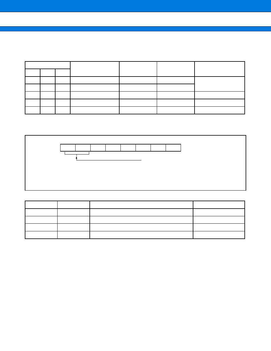
PRODUCT LINEUP
MB91133
MB91F133
MB91FV130
CLASSIFICATION
MASK ROM device
(mass production item)
FLASH ROM device
(for evaluation)
Piggy/EVA device
(for evaluation /
development)
RAM capacity
6 KB
6 KB
6 KB
CROM capacity
254 KB
FLASH capacity
254 KB
254 KB
CRAM capacity
2 KB
2 KB
2 KB
Others
Mass production
Trial production
Provided
MB91133/MB91F133
4
s
PIN ASSIGNMENTS
∑ MB91FV130
(BOTTOM VIEW)
(PGA-299C-A01)
3
2
5
8
25
27
32
34
22
29
37
50
53
45
49
52
57
68
71
74
299 296 293 277 274 270 268 278 275 262 254 247 257 252 250 245 233 230 224
298 292 289 286 283 280 276 269 264 263 258 251 248 243 240 237 234 225 221
10
4
297 291 287 284 279 271 265 261 256 249 242 239 235 229 228 219 218
13
6
300 295 290 285 281 272 267 259 255 246 241 236 231 226 223 215 207
16
11
7
1
294 288 282 273 266 260 253 244 238 232 227 222 217 212 202
19
15
12
9
220 216 213 209 199
23
18
17
14
214 211 210 205 195
26
24
21
20
208 206 204 201 203
33
31
30
28
198 197 196 194 200
39
38
35
36
192 193 191 190 187
40
41
43
42
186 185 188 189 179
44
46
47
48
178 180 181 183 172
51
54
56
58
170 171 174 176 184
55
60
61
64
164 167 168 173 182
59
63
66
70
159 162 165 169 177
62
67
72
77
82
88
94
103 110 116 123 133 139 145 153 157 161 166 175
65
73
76
81
86
91
96
105 109 117 122 131 136 141 147 151 156 163 158
69
78
79
85
89
92
99
106 111 115 121 129 135 138 142 148 154 160 155
75
84
87
90
93
98
101 108 113 114 119 126 130 134 137 140 144 150 152
80
83
95
100 102 107
97
104 112 125 128 118 120 124 127 132 143 146 149
MB91133/MB91F133
5
∑ MB91F133/MB91133
(TOP VIEW)
(BGA-144P-M01)
14
13
12
11
10
9
8
7
6
5
4
3
2
1
A
B
C
D
E
F
G
H
J
K
L
M
N
P
INDEX
108
107
106
110
109
105
111
112
113
102
103
104
99
100
101
96
97
98
95
92
93
91
94
89
88
90
85
84
86
82
81
83
79
78
80
75
76
77
74
73
69
72
71
70
87
115
114
116
118
117
119
121
120
122
125
124
126
123
128
129
127
130
132
133
134
131
135
136
137
138
139
140
142
141
5
8
143
1
4
6
144
2
3
7
11
9
10
14
12
13
18
15
16
17
19
22
21
20
26
23
25
24
29
28
27
32
31
30
41
44
47
50
54
51
55
58
62
65
68
59
33
34
40
42
45
48
52
57
61
64
67
37
35
39
43
46
49
53
56
60
63
66
38
36
MB91133/MB91F133
6
∑ MB91F133/MB91133
(TOP VIEW)
(FPT-144P-M08)
1
2
3
4
5
6
7
8
9
10
11
12
13
14
15
16
17
18
19
20
21
22
23
24
25
26
27
28
29
30
31
32
33
34
35
36
37
38
39
40
41
42
43
44
45
46
47
48
49
50
51
52
53
54
55
56
57
58
59
60
61
62
63
64
65
66
67
68
69
70
71
72
108
107
106
105
104
103
102
101
100
99
98
97
96
95
94
93
92
91
90
89
88
87
86
85
84
83
82
81
80
79
78
77
76
75
74
73
144
143
142
141
140
139
138
137
136
135
134
133
132
131
130
129
128
127
126
125
124
123
122
121
120
119
118
117
116
115
114
113
112
111
110
109
P20/D16
P21/D17
P22/D18
P23/D19
P24/D20
P25/D21
P26/D22
P27/D23
V
SS
P30/D24
P31/D25
P32/D26
P33/D27
P34/D28
P35/D29
P36/D30
P37/D31
P40/A00
P41/A01
P42/A02
P43/A03
P44/A04
P45/A05
P46/A06
P47/A07
V
SS
V
CC
5
P50/A08
P51/A09
P52/A10
P53/A11
P54/A12
P55/A13
P56/A14
P57/A15
P60/A16/INT16
MD2
MD1
MD0
V
SS
X1
X0
V
CC
3
X1A
X0A
V
SS
RST
PL7/DACK2
PL6/DREQ2
PL5/DEOP1
PL4/DACK1
PL3/DREQ1
PL2/DEOP0
PL1/DACK0
PL0/DREQ0
PK7/AN7/CMP
PK6/AN6
PK5/AN5
PK4/AN4
PK3/AN3
PK2/AN2
PK1/AN1
PK0/AN0
AV
SS
AVRL
AVRH
AV
CC
DAVC
DAVS
DA0
DA1
DA2
V
CC
5
PH0/SIN0
PH1/SOT0
PH2/SCK0
PI0/SIN1
PI1/SOT1
PI2/SCK1
PI3/SIN2
PI4/SOT2
PI5/SCK2
PJ0/SIN3
PJ1/SOT3
PJ2/SCK3
PJ3/SIN4
PJ4/SOT4
PJ5/SCK4
V
CC
3
V
SS
PG5/PPG5
PG4/PPG4
PG3/PPG3
PG2/PPG2
PG1/PPG1
PG0/PPG0
PF7/RTO7
PF6/RTO6
PF5/RTO5
PF4/RTO4
PF3/RTO3
PF2/RTO2
PF1/RTO1
PF0/RTO0
PE7/DTTI
PE6/FRCK
PE5/IN3
PE4/IN2
P61/A17/INT17
P62/A18/INT18
P63/A19/INT19
P64/A20/INT20
P65/A21/INT21
P66/A22/INT22
P67/A23/INT23
V
CC
3
P80/RDY
P81/BGRNT
P82/BRQ
P83/RD
P84/WR0
P85/WR1
P86/CLK
V
SS
PC0/INT0
PC1/INT1
PC2/INT2
PC3/INT3
PC4/AIN0/INT4
PC5/BIN0/INT5
PC6/AIN1/INT6
PC7/BIN1/INT7
PD0/INT8/TRG0
PD1/INT9/TRG1
PD2/INT10/TRG2
PD3/INT11/TRG3
PD4/INT12/TRG4
PD5/INT13/TRG5
PD6/DEOP2/INT14
PD7/ATG/INT15
PE0/ZIN0
PE1/ZIN1
PE2/IN0
PE3/IN1
MB91133/MB91F133
7
s
PIN NUMBERS LIST
∑ Device : MB91FV130
Package : PGA-299C-A01
(Continued)
No.
Pin Name
No.
Pin Name
No.
Pin Name
No.
Pin Name
1
P20/D16
35
P54/A12
69
N.C.
103
PK3/AN3
2
V
SS
36
P55/A13
70
N.C.
104
V
CC
5
3
OPEN
37
V
CC
5
71
V
SS
105
PK4/AN4
4
P21/D17
38
P56/A14
72
N.C.
106
PK5/AN5
5
V
CC
5
39
P57/A15
73
N.C.
107
PK6/AN6
6
P22/D18
40
P60/A16/INT16
74
V
CC
5
108
PK7/AN7/CMP
7
P23/D19
41
P61/A17/INT17
75
N.C.
109
DAVC
8
V
SS
42
P62/A18/INT18
76
MD0
110
DAVS
9
P24/D20
43
P63/A19/INT19
77
MD1
111
DA0
10
P25/D21
44
P64/A20/INT20
78
MD2
112
V
SS
11
P26/D22
45
P65/A21/INT21
79
V
CC
3
113
DA1
12
P27/D23
46
P66/A22/INT22
80
V
SS
114
DA2
13
P30/D24
47
P67/A23/INT23
81
X0
115
PH0/SIN0
14
P31/D25
48
P80/RDY
82
X1
116
PH1/SOT0
15
P32/D26
49
V
CC
3
83
V
CC
5
117
PH2/SCK0
16
P33/D27
50
V
SS
84
RST
118
PI0/SIN1
17
P34/D28
51
P81/BGRNT
85
N.C.
119
PI1/SOT1
18
P35/D29
52
P82/BRQ
86
ICLK
120
PI2/SCK1
19
P36/D30
53
V
CC
5
87
ICS0
121
PI3/SIN2
20
P37/D31
54
P83/RD
88
ICS1
122
PI4/SOT2
21
P40/A00
55
P84/WR0
89
ICS2
123
PI5/SCK2
22
V
CC
5
56
P85/WR1
90
ICD0
124
PJ0/SIN3
23
P41/A01
57
P86/CLK
91
ICD1
125
V
CC
5
24
P42/A02
58
PL0/DREQ0
92
ICD2
126
PJ1/SOT3
25
P43/A03
59
PL1/DACK0
93
ICD3
127
PJ2/SCK3
26
P44/A04
60
PL2/DEOP0
94
BREAK
128
V
SS
27
P45/A05
61
PL3/DREQ1
95
AV
CC
129
V
CC
3
28
P46/A06
62
PL4/DACK1
96
AVRH
130
X0A
29
V
SS
63
PL5/DEOP1
97
V
SS
131
X1A
30
P47/A07
64
PL6/DREQ2
98
AVRL
132
V
SS
31
P50/A08
65
PL7/DACK2
99
AV
SS
133
PJ3/SIN4
32
P51/A09
66
N.C.
100
PK0/AN0
134
PJ4/SOT4
33
P52/A10
67
N.C.
101
PK1/AN1
135
PJ5/SCK4
34
P53/A11
68
V
CC
5
102
PK2/AN2
136
PC0/INT0
MB91133/MB91F133
8
(Continued)
No.
Pin Name
No.
Pin Name
No.
Pin Name
No.
Pin Name
No.
Pin Name
137
PC1/INT1
173
PF5/RTO5
209
TAD14
245
TDT23
281
TDT53
138
PC2/INT2
174
PF6/RTO6
210
TAD15
246
TDT24
282
TDT54
139
PC3/INT3
175
PF7/RTO7
211
V
CC
3
247
V
SS
283
TDT55
140
PC4/INT4/AIN0
176
PG0/PPG0
212
TOE
248
TDT25
284
TDT56
141
PC5/INT5/BIN0
177
PG1/PPG1
213
TCE1
249
TDT26
285
TDT57
142
PC6/INT6/AIN1
178
PG2/PPG2
214
TADSC
250
TDT27
286
V
CC
3
143
V
CC
5
179
V
SS
215
TWR
251
TDT28
287
TDT58
144
PC7/INT7/BIN1
180
PG3/PPG3
216
TDT00
252
TDT29
288
TDT59
145
PD0/INT8/TRG0
181
PG4/PPG4
217
TDT01
253
TDT30
289
TDT60
146
V
SS
182
PG5/PPG5
218
V
SS
254
V
CC
5
290
TDT61
147
PD1/INT9/TRG1
183
N.C.
219
TDT02
255
TDT31
291
TDT62
148
PD2/INT10/TRG2
184
N.C.
220
TDT03
256
TDT32
292
TDT63
149
V
CC
5
185
N.C.
221
V
CC
5
257
TDT33
293
V
CC
5
150
PD3/INT11/TRG3
186
N.C.
222
TDT04
258
TDT34
294
TDT64
151
PD4/INT12/TRG4
187
V
CC
5
223
TDT05
259
TDT35
295
TDT65
152
V
SS
188
EXRAM
224
V
SS
260
TDT36
296
V
SS
153
PD5/INT13/TRG5
189
TAD00
225
TDT06
261
TDT37
297
TDT66
154
PD6/INT14/DEOP2
190
TAD01
226
TDT07
262
V
SS
298
TDT67
155
V
CC
5
191
TAD02
227
TDT08
263
TDT38
299
V
CC
5
156
PD7/INT15/ATG
192
TAD03
228
TDT09
264
TDT39
300
TDT68
157
PE0/ZIN0
193
V
CC
3
229
TDT10
265
TDT40
158
V
SS
194
TAD04
230
V
CC
5
266
TDT41
159
PE1/ZIN1
195
TAD05
231
TDT11
267
TDT42
160
PE2/IN0
196
TAD06
232
TDT12
268
TDT43
161
PE3/IN1
197
TAD07
233
V
SS
269
V
CC
3
162
PE4/IN2
198
TAD08
234
TDT13
270
TDT44
163
PE5/IN3
199
TAD09
235
TDT14
271
TDT45
164
PE6/FRCK
200
V
SS
236
TDT15
272
TDT46
165
PE7/DTTI
201
TAD10
237
TDT16
273
TDT47
166
V
CC
3
202
TAD11
238
TDT17
274
TDT48
167
PF0/RTO0
203
V
CC
5
239
TDT18
275
V
CC
5
168
PF1/RTO1
204
TAD12
240
V
CC
3
276
TDT49
169
PF2/RTO2
205
TAD13
241
TDT19
277
TDT50
170
PF3/RTO3
206
TAD14
242
TDT20
278
V
SS
171
PF4/RTO4
207
TAD15
243
TDT21
279
TDT51
172
V
CC
5
208
TCLK
244
TDT22
280
TDT52
MB91133/MB91F133
9
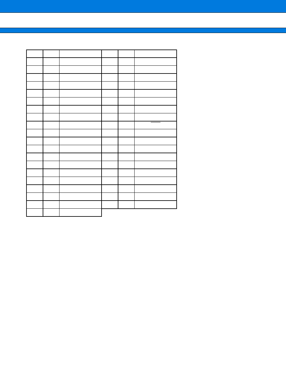
∑ Device : MB91F133/MB91133
Package : BGA-144P-M01/FPT-144P-M08
(Continued)
LQFP FBGA
Pin Name
LQFP FBGA
Pin Name
LQFP FBGA
Pin Name
1
B2
P20/D16
36
P1
P60/A16/INT16
71
P13
PE2/IN0
2
B1
P21/D17
37
N2
P61/A17/INT17
72
P14
PE3/IN1
3
C1
P22/D18
38
P2
P62/A18/INT18
73
N13
PE4/IN2
4
C2
P23/D19
39
P3
P63/A19/INT19
74
N14
PE5/IN3
5
C3
P24/D20
40
N3
P64/A20/INT20
75
M14
PE6/FRCK
6
D2
P25/D21
41
M3
P65/A21/INT21
76
M13
PE7/DTTI
7
D1
P26/D22
42
N4
P66/A22/INT22
77
M12
PF0/RTO0
8
D3
P27/D23
43
P4
P67/A23/INT23
78
L13
PF1/RTO1
9
E2
V
SS
44
M4
V
CC
3
79
L14
PF2/RTO2
10
E1
P30/D24
45
N5
P80/RDY
80
L12
PF3/RTO3
11
E3
P31/D25
46
P5
P81/BGRNT
81
K13
PF4/RTO4
12
F2
P32/D26
47
M5
P82/BRQ
82
K14
PF5/RTO5
13
F1
P33/D27
48
N6
P83/RD
83
K12
PF6/RTO6
14
F3
P34/D28
49
P6
P84/WR0
84
J13
PF7/RTO7
15
G4
P35/D29
50
M6
P85/WR1
85
J14
PG0/PPG0
16
G2
P36/D30
51
L7
P86/CLK
86
J12
PG1/PPG1
17
G1
P37/D31
52
N7
V
SS
87
H11
PG2/PPG2
18
G3
P40/A00
53
P7
PC0/INT0
88
H13
PG3/PPG3
19
H3
P41/A01
54
M7
PC1/INT1
89
H14
PG4/PPG4
20
H1
P42/A02
55
M8
PC2/INT2
90
H12
PG5/PPG5
21
H2
P43/A03
56
P8
PC3/INT3
91
G12
V
SS
22
H4
P44/A04
57
N8
PC4/AIN0/INT4
92
G14
V
CC
3
23
J4
P45/A05
58
L8
PC5/BIN0/INT5
93
G13
PJ5/SCK4
24
J1
P46/A06
59
L9
PC6/AIN1/INT6
94
G11
PJ4/SOT4
25
J2
P47/A07
60
P9
PC7/BIN1/INT7
95
F11
PJ3/SIN4
26
J3
V
SS
61
N9
PD0/INT8/TRG0
96
F14
PJ2/SCK3
27
K1
V
CC
5
62
M9
PD1/INT9/TRG1
97
F13
PJ1/SOT3
28
K2
P50/A08
63
P10
PD2/INT10/TRG2
98
F12
PJ0/SIN3
29
K3
P51/A09
64
N10
PD3/INT11/TRG3
99
E14
PI5/SCK2
30
L1
P52/A10
65
M10
PD4/INT12/TRG4
100
E13
PI4/SOT2
31
L2
P53/A11
66
P11
PD5/INT13/TRG5
101
E12
PI3/SIN2
32
L3
P54/A12
67
N11
PD6/DEOP2/INT14
102
D14
PI2/SCK1
33
M2
P55/A13
68
M11
PD7/ATG/INT15
103
D13
PI1/SOT1
34
M1
P56/A14
69
N12
PE0/ZIN0
104
D12
PI0/SIN1
35
N1
P57/A15
70
P12
PE1/ZIN1
105
C13
PH2/SCK0
MB91133/MB91F133
10
(Continued)
LQFP FBGA
Pin Name
LQFP FBGA
Pin Name
106
C14
PH1/SOT0
126
C8
PL0/DREQ0
107
B14
PH0/SIN0
127
C7
PL1/DACK0
108
A14
V
CC
5
128
A7
PL2/DEOP0
109
B13
DA2
129
B7
PL3/DREQ1
110
A13
DA1
130
D7
PL4/DACK1
111
B12
DA0
131
D6
PL5/DEOP1
112
A12
DAVS
132
A6
PL6/DREQ2
113
C12
DAVC
133
B6
PL7/DACK2
114
B11
AV
CC
134
C6
RST
115
A11
AVRH
135
A5
V
SS
116
C11
AVRL
136
B5
X0A
117
B10
AV
SS
137
C5
X1A
118
A10
PK0/AN0
138
A4
V
CC
3
119
C10
PK1/AN1
139
B4
X0
120
B9
PK2/AN2
140
C4
X1
121
A9
PK3/AN3
141
B3
V
SS
122
C9
PK4/AN4
142
A3
MD0
123
D8
PK5/AN5
143
A2
MD1
124
B8
PK6/AN6
144
A1
MD2
125
A8
PK7/AN7/CMP

MB91133/MB91F133
11
s
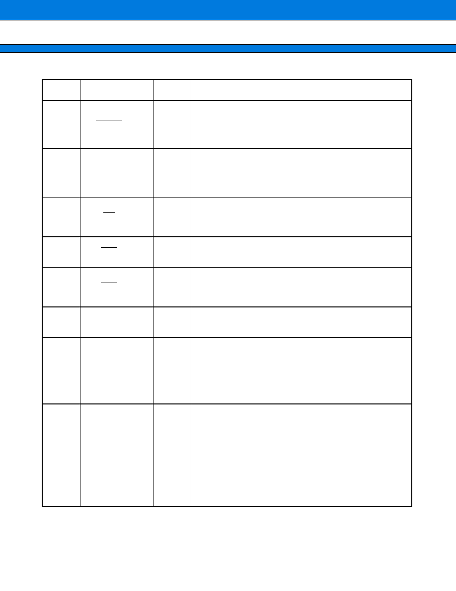
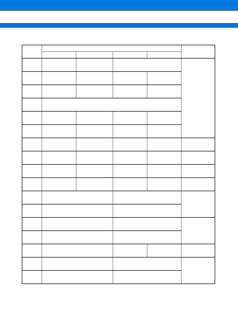
PIN DESCRIPTIONS
(Continued)
Pin No.
Pin name
Circuit
type
Function
1
2
3
4
5
6
7
8
D16/P20
D17/P21
D18/P22
D19/P23
D20/P24
D21/P25
D22/P26
D23/P27
C
External data bus bits 16 to 23
Only valid for external bus 16-bit mode. Can be used as ports in
single-chip and external bus 8-bit modes.
10
11
12
13
14
15
16
17
D24/P30
D25/P31
D26/P32
D27/P33
D28P34
D29/P35
D30/P36
D31/P37
C
External data bus bits 24 to 31
Can be used as ports in single-chip mode.
18
19
20
21
22
23
24
25
28
29
30
31
32
33
34
35
A00/P40
A01/P41
A02/P42
A03/P43
A04/P44
A05/P45
A06/P46
A07/P47
A08/P50
A09/P51
A10/P52
A11/P53
A12/P54
A13/P55
A14/P56
A15/P57
F
External address bus bits 0 to 15
Valid for external bus mode. Can be used as ports in single-chip
mode.
36
37
38
39
40
41
42
43
A16/INT16/P60
A17/INT17/P61
A18/INT18/P62
A19/INT19/P63
A20/INT20/P64
A21/INT21/P65
A22/INT22/P66
A23/INT23/P67
O
External address bus bits 16 to 23
[ INT16 to 23 ] are external interruption request inputs 16 to 23.
These inputs are always used when dealing with external interrup-
tions is permitted, so output by ports should be stopped except
when carried out intentionally.
Can be used as ports when address bus and external interruption
request input are not used.
45
RDY/P80
C
External RDY input
This function is valid when external RDY input is permitted. "0" is
input if the bus cycle being executed is not completed.
Can be used as a port when the external RDY input is not used.
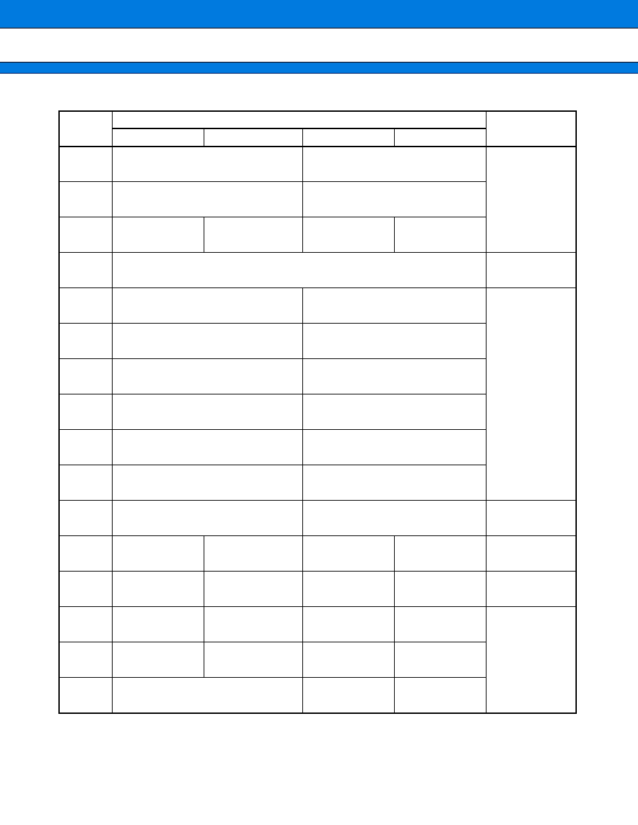
MB91133/MB91F133
12
(Continued)
Pin No.
Pin name
Circuit
type
Function
46
BGRNT/P81
F
External bus open reception output
This function is valid when external bus open reception output is
permitted. "L" is output if the external bus is opened. Can be used
as a port when the external bus open reception output is prohibit-
ed.
47
BRQ/P82
C
External bus open request input
This function is valid when external bus open request input is per-
mitted. "1" is input if the external bus requests to be opened.
Can be used as a port when the external bus open request input is
not used.
48
RD/P83
F
External bus read strobe output
This function is valid when external bus read strobe output is per-
mitted. Can be used as a port when the external bus read strobe
output is prohibited.
49
WR0/P84
F
External bus write strobe output
This function is valid in external bus mode. Can be used as a port
in single-chip mode.
50
WR1/P85
F
External bus write strobe output
This function is valid in external bus mode and with 16-bit buses.
Can be used as a port in single-chip mode or with external 8-bit
bus.
51
CLK/P86
F
System clock output
Outputs the same clock frequency as the external bus operation.
Can be used as a port when it is not otherwise used.
53
54
55
56
INT0/PC0
INT1/PC1
INT2/PC2
INT3/PC3
H
External interruption request inputs 0 to 3
These inputs are always used when dealing with external interrup-
tions is permitted, so output by ports should be stopped except
when carried out intentionally.
Can be used to reset standby as input is permitted in this port un-
der standby status.Can be used as ports when external interrup-
tion request input is not used.
57
58
59
60
AIN0/INT4/PC4
BIN0/INT5/PC5
AIN1/INT6/PC6
BIN1/INT7/PC7
H
External interruption request inputs 4 to 7
These inputs are always used when dealing with external interrup-
tions is permitted, so output by ports should be stopped except
when carried out intentionally. Can be used to reset standby as in-
put is permitted in these ports under standby status.
[ AIN, BIN ] Up/down timer input
This input is always used when input is permitted, so output by
ports should be stopped except when carried out intentionally.
Can be used as a port when external interruption request input and
up/down timer input are not used.
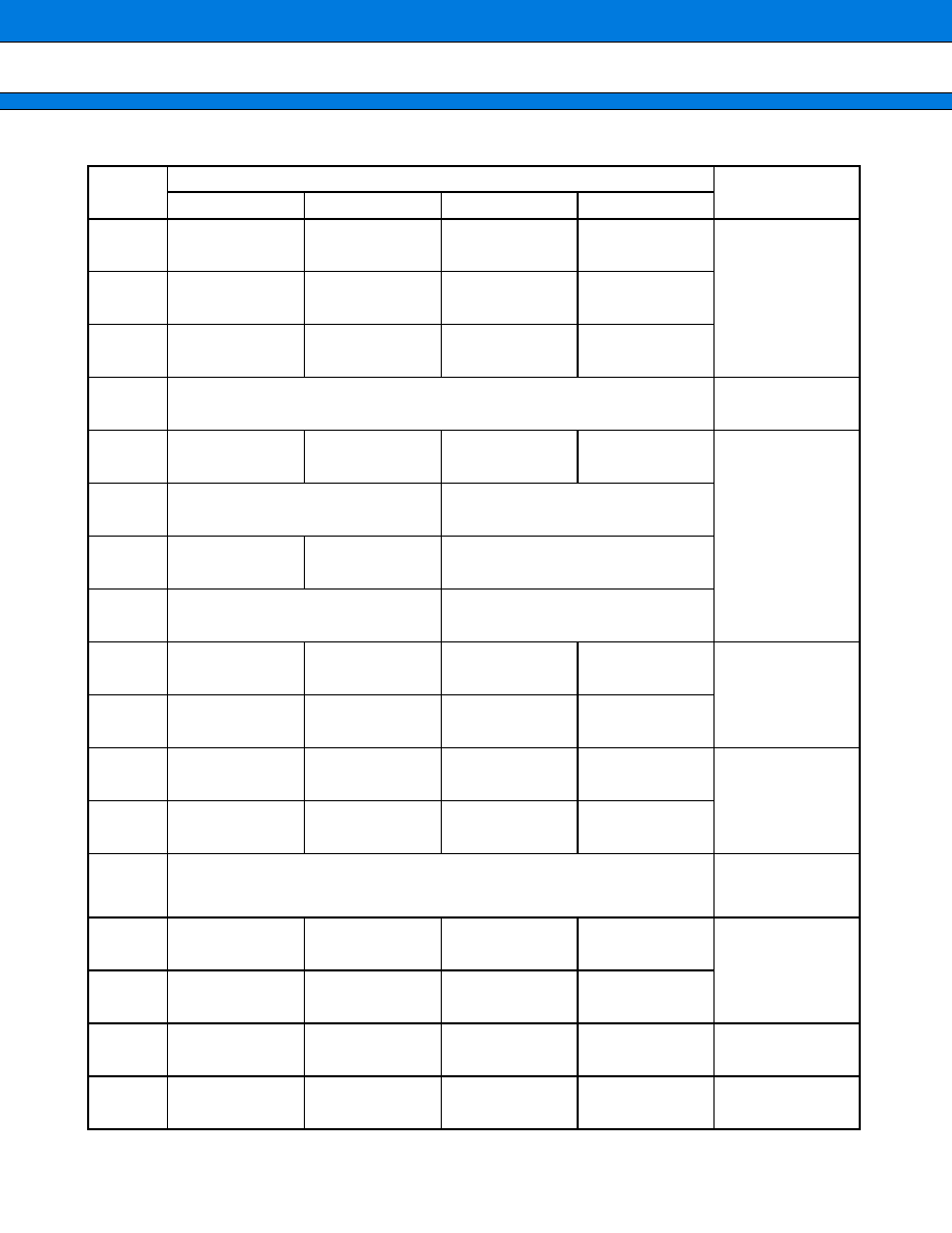
MB91133/MB91F133
13
(Continued)
Pin No.
Pin name
Circuit
type
Function
61
62
63
64
65
66
67
68
TRG0/INT8/PD0
TRG1/INT9/PD1
TRG2/INT10/PD2
TRG3/INT11/PD3
TRG4/INT12/PD4
TRG5/INT13/PD5
DEOP2/INT14/PD6
ATG/INT15/PD7
O
External interruption request inputs 8 to 15
These inputs are always used when dealing with external interrup-
tions is permitted, so output by ports should be stopped except
when carried out intentionally.
[ TRG0 to 5 ] These are external trigger inputs for PPG timers.
[ DEOP2 ] DMA external transfer termination output
This function is valid when external transfer termination output
specification of the DMA controller is permitted.
[ ATG ] A/D converter external trigger input
These inputs are always used when they are selected as A/D initi-
ation factors, so output by ports should be stopped except when
carried out intentionally. Can be used as ports when not otherwise
used.
69
70
ZIN0/PE0
ZIN1/PE1
O
Up/down timer input
These inputs are always used when input is permitted, so output
by ports should be stopped except when carried out intentionally.
Can be used as ports when up/down timer input is not used.
71
72
73
74
IN0/PE2
IN1/PE3
IN2/PE4
IN3/PE5
F
Input capture input
This function is valid when input capture activates input. Can be
used as ports when input capture input is not used.
75
FRCK/PE6
F
External clock input pin of free-run timer
Can be used as a port when external clock input of free-run timer
is not used.
76
DTTI/PE7
F
RTOn pin level fixed input
Invalid when input is permitted in the waveform generation area.
Can be used as a port when RTOn pin level fixed input is not used.
77
78
79
80
81
82
83
84
RTO0/PF0
RTO1/PF1
RTO2/PF2
RTO3/PF3
RTO4/PF4
RTO5/PF5
RTO6/PF6
RTO7/PF7
F
Output compare event pins/waveform output pins in the
waveform generation area
Can be used as ports when specification of the output compare
event pin/waveform output pin of the waveform generation area is
prohibited.
85
86
87
88
89
90
PPG0/PG0
PPG1/PG1
PPG2/PG2
PPG3/PG3
PPG4/PG4
PPG5/PG5
F
PPG timer output
This function is valid when output specification of the PPG timer is
permitted. Can be used as ports when output specification of the
PPG timer is prohibited.
111
110
109
DA0
DA1
DA2
D/A converter output
This function is valid when output specification of the D/A converter
is permitted.

MB91133/MB91F133
14
(Continued)
Pin No.
Pin name
Circuit
type
Function
107
SIN0/PH0
P
UART0 data input
This input is always used when UART0 activates input, so output
by ports should be stopped except when carried out intentionally.
Can be used as a port when UART0 data input is not used.
106
SOT0/PH1
P
UART0 data output
This function is valid when UART0 data output specification is per-
mitted. Can be used as a port when UART0 data output specifica-
tion is prohibited.
105
SCK0/PH2
P
UART0 clock input/output
This function is valid when UART0 clock output specification is per-
mitted. Can be used as a port when UART0 clock output specifi-
cation is prohibited.
104
SIN1/PI0
P
UART1 data input
This input is always used when UART1 activates input, so output
by ports should be stopped except when carried out intentionally.
Can be used as a port when UART1 data input is not used.
103
SOT1/PI1
P
UART1 data output
This function is valid when UART1 data output specification is per-
mitted. Can be used as a port when UART1 data output specifica-
tion is prohibited.
102
SCK1/PI2
P
UART1 clock input/output
This function is valid when UART1 clock output specification is per-
mitted. Can be used as a port when UART1 clock output specifi-
cation is prohibited.
101
SIN2/PI3
P
UART2 data input
This input is always used when UART2 activates input, so output
by ports should be stopped except when carried out intentionally.
Can be used as a port when UART2 data input is not used.
100
SOT2/PI4
P
UART2 data output
This function is valid when UART2 data output specification is per-
mitted. Can be used as a port when UART2 data output specifica-
tion is prohibited.
99
SCK2/PI5
P
UART2 clock input/output
This function is valid when UART2 clock output specification is per-
mitted. Can be used as a port when UART2 clock output specifi-
cation is prohibited.
98
SIN3/PJ0
P
UART3 data input
This input is always used when UART3 activates input, so output
by ports should be stopped except when carried out intentionally.
Can be used as a port when UART3 data input is not used.
97
SOT3/PJ1
P
UART3 data output
This function is valid when UART3 data output specification is per-
mitted. Can be used as a port when UART3 data output specifica-
tion is prohibited.

MB91133/MB91F133
15
(Continued)
Pin No.
Pin name
Circuit
type
Function
96
SCK3/PJ2
P
UART3 clock input/output
This function is valid when UART3 clock output specification is per-
mitted. Can be used as a port when UART3 clock output specifi-
cation is prohibited.
95
SIN4/PJ3
P
UART4 data input
This input is always used when UART4 activates input, so output
by ports should be stopped except when carried out intentionally.
Can be used as a port when UART4 data input is not used.
94
SOT4/PJ4
P
UART4 data output
This function is valid when UART4 data output specification is per-
mitted. Can be used as a port when UART4 data output specifica-
tion is prohibited.
93
SCK4/PJ5
P
UART4 clock input/output
This function is valid when UART4 clock output specification is per-
mitted. Can be used as a port when UART4 clock output specifi-
cation is prohibited.
118
119
120
121
122
123
124
125
AN0/PK0
AN1/PK1
AN2/PK2
AN3/PK3
AN4/PK4
AN5/PK5
AN6/PK6
CMP/AN7/PK7
N
A/D converter analog input
This is valid when the AICK register specification is analog input.
[ CMP ] level comparator input
Can be used as ports when A/D converter analog input is not used.
126
DREQ0/PL0
F
DMA external transfer request input
This input is always used if selected as the transfer factor for the
DMA controller, so output by ports should be stopped except when
carried out intentionally. Can be used as a port when DMA exter-
nal transfer request input is not used.
127
DACK0/PL1
F
DMA external transfer request reception output
This function is valid when external transfer request reception out-
put specification of the DMA controller is permitted. Can be used
as a port when transfer request reception output specification of
the DMA controller is prohibited.
128
DEOP0/PL2
F
DMA external transfer termination output
This function is valid when external transfer termination output
specification of the DMA controller is permitted.
129
DREQ1/PL3
F
DMA external transfer request input
This input is always used if selected as the transfer factor for the
DMA controller, so output by ports should be stopped except when
carried out intentionally. Can be used as a port when DMA exter-
nal transfer request input is not used.
MB91133/MB91F133
16
(Continued)
Note : In most of the above pins, the input/output of the I/O ports and resources are multiplexed, such as xxxx/Pxx.
If the output from ports and resources of those pins compete with each other, the resource is given priority.
Pin No.
Pin name
Circuit
type
Function
130
DACK1/PL4
F
DMA external transfer request reception output
This function is valid when external transfer request reception out-
put specification of the DMA controller is permitted. Can be used
as a port when transfer request reception output specification of
the DMA controller is prohibited.
131
DEOP1/PL5
F
DMA external transfer termination output
This function is valid when external transfer termination output
specification of the DMA controller is permitted.
132
DREQ2/PL6
F
DMA external transfer request input
This input is always used if selected as the transfer factor for the
DMA controller, so output by ports should be stopped except when
carried out intentionally. Can be used as a port when DMA exter-
nal transfer request input is not used.
133
DACK2/PL7
F
DMA external transfer request reception output
This function is valid when external transfer request reception out-
put specification of the DMA controller is permitted. Can be used
as a port when transfer request reception output specification of
the DMA controller is prohibited.
134
RST
B
External reset input
136
137
X0A
X1A
K
Oscillation pin for low-speed clock (32 kHz)
139
140
X0
X1
A
Oscillation pin for high-speed clock (16.5 MHz)
142
143
144
MD0
MD1
MD2
G
Mode pins
Basic MCU operation mode is set by these pins. They should be
directly connected to V
CC
or V
SS
for use.
112
DAVS
Ground pin of D/A converter (connected to analog ground)
113
DAVC
Power pin of D/A converter
114
AV
CC
Power pin for A/D converter
115
AVRH
Reference voltage pin for A/D converter (high electric poten-
tial side)
When this pin is turned on/off, AVRH or more electric potential
must be supplied to V
CC
.
116
AVRL
Reference voltage pin for A/D converter (low electric potential
side)
117
AV
SS
Ground pin for A/D converter (connected to analog ground)
27, 108
V
CC
5
5 V power of digital circuit
Power must be connected to all V
CC
5 pins for use.
44, 92
138
V
CC
3
3 V power of digital circuit
Power must be connected to all V
CC
3 pins for use.
9, 26, 52,
91, 135,
141
V
SS
Ground level of digital circuit
MB91133/MB91F133
17
s
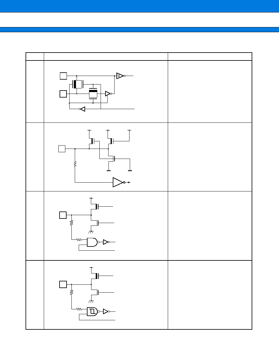
INPUT/OUTPUT CIRCUIT TYPES
(Continued)
Type
Circuit
Remarks
A
∑ High-speed oscillation circuit
(16.5 MHz)
Oscillation feedback resistance
=
approximately 1 M
3 V CMOS level input
B
∑ With pull up resistance
CMOS level input
Pull-up resistance value
=
approximately 25 k
(Typ.)
C
∑ CMOS level input/output pin
CMOS level output
CMOS level input
(with standby control)
I
OL
=
4 mA
F
∑ CMOS hysteresis input/output pin
CMOS level output
CMOS hysteresis input
(with standby control)
I
OL
=
4 mA
X1
X0
Xout
Standby control signal
Digital input
Pout
Nout
CMOS input
Standby control
R
Pout
Nout
Hysteresis input
Standby control
R
MB91133/MB91F133
18
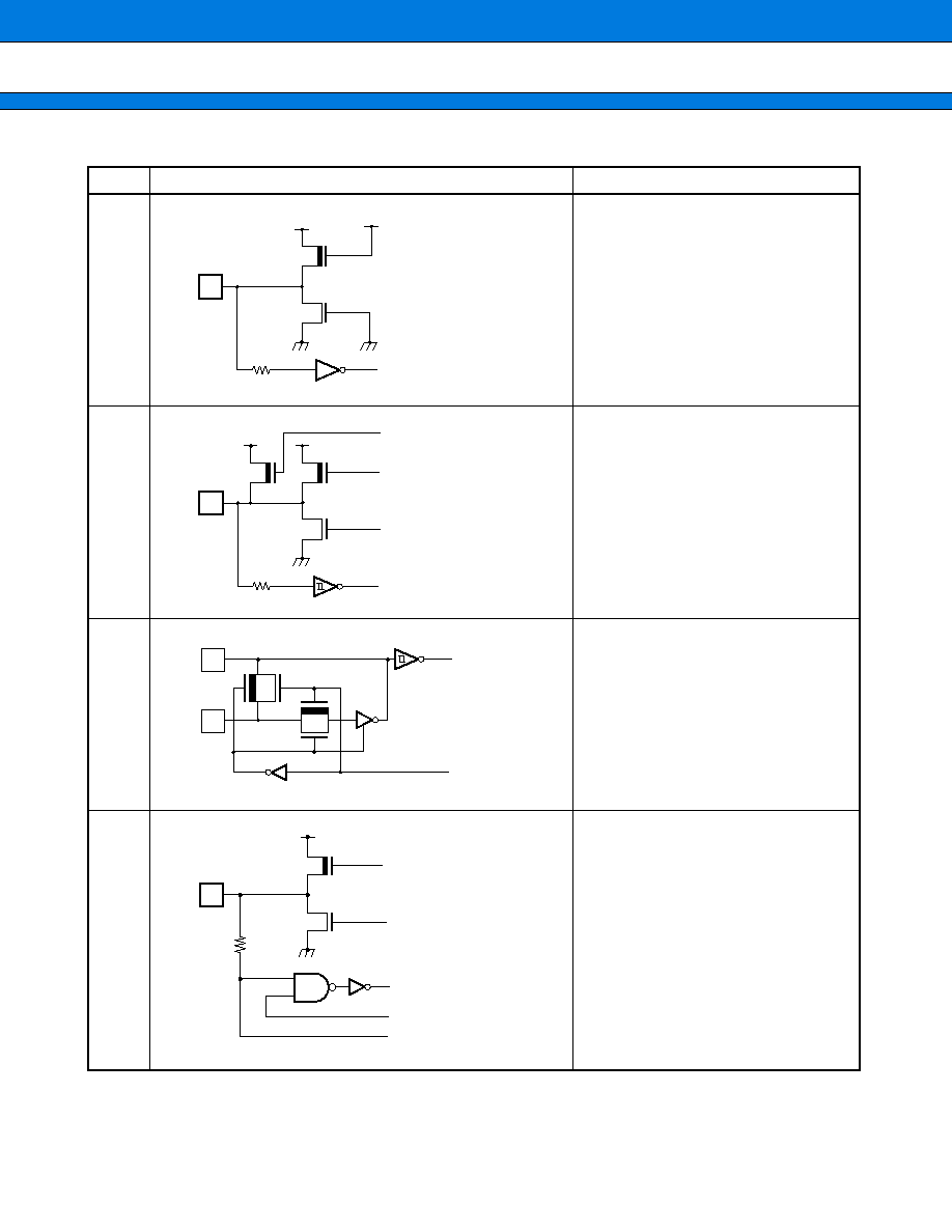
(Continued)
Type
Circuit
Remarks
G
∑ CMOS level input pin
CMOS level input
(without standby control)
I
OL
=
4 mA
H
∑ CMOS hysteresis input/output pin
with pull- up control
CMOS level output
CMOS hysteresis input
(without standby control)
Pull-up resistance value
=
approximately 50 k
(Typ.)
I
OL
=
4 mA
K
∑ Clock oscillation circuit (32 kHz)
Oscillation feedback resistance
=
approximately 4.5 M
/3 V
3 V CMOS level input
N
∑ Analog/CMOS level input/output pin
CMOS level output
CMOS level input
(with standby control)
Analog input
(Analog input is valid when bit dealt
by AIC is "1".)
I
OL
=
4 mA
R
Digital input
R
R
Pout
Pull-up control
Hysteresis input
Nout
X1A
X0A
Xout
Standby control signal
Pout
CMOS input
Standby control
Analog input
Nout
R
MB91133/MB91F133
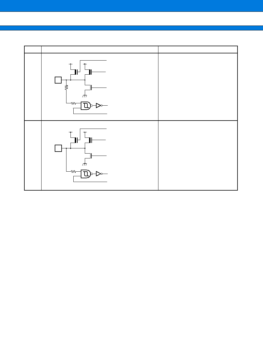
19
(Continued)
Type
Circuit
Remarks
O
∑ CMOS hysteresis input/output pin
with pull-up control
CMOS level output
CMOS hysteresis input
(with standby control)
Pull-up resistance value
=
approximately 50 k
(Typ.)
I
OL
=
4 mA
P
∑ CMOS hysteresis input/output pin
with pull-up control
CMOS level output
(with open-drain control)
CMOS hysteresis input
(with standby control)
Pull-up resistance value
=
approximately 50 k
(Typ)
I
OL
=
4 mA
Pout
Pull-up control
Hysteresis input
Standby control
Nout
R
R
Nout
Pull-up control
Open-drain control
Hysteresis input
Standby control
R
R

MB91133/MB91F133
20
s
HANDLING DEVICES
1.
Points to Note on Handling Devices
(1) Latch-up prevention
Latch-up may occur by CMOS IC if a voltage in excess of V
CC
5 or lower than V
SS
is applied to the input/output
pins, or if the voltage exceeds the rating between V
CC
5 and V
SS
. If latch-up occurs, the electrical current increases
significantly and may destroy certain components due to excessive heat, so great care must be taken to ensure
that the maximum rating is not exceeded during use.
(2) Handling Pins
∑ Handling unused pins
Input pins that are not used should be pulled up or down as they may cause erroneous operations if left open.
∑ Handling N.C. pins
N.C. pins must be opened for use.
∑ Handling output pins
Excessive electric current may flow if the output pin is shorted by the power source or other output pins, or
connected to large loads. If such status is prolonged, the device is liable to be damaged, so great care must
be taken to ensure that the usage volume does not exceed the maximum rating.
∑ Mode pins (MD0 to MD2)
Those pins must be directly connected to V
CC
5 or V
SS
for use.
Pattern lengths between V
CC
5 or V
SS
and each mode pin on the printed-circuit board should be arranged to
be as short as possible to prevent the test mode from being erroneously turned on due to noise, and they
should be connected with low impedance.
∑ Power pins
When there are a number of V
CC
5/V
CC
3/V
SS
, those whose electrical potential must be the same within the
device are connected to prevent erroneous operation such as latch-up for device design purposes, but those
must be externally connected to a power source and earthed to follow the general output current standard and
prevent erroneous operation of strobe signals due to increased ground level and reduction in unnecessary
radiation.
Care must also be taken to ensure that they are connected to the V
CC
5/V
SS
or V
CC
3/V
SS
of this device at the
lowest possible impedance from the source of the electrical current supply.
Furthermore, it is recommended that a ceramic capacitor of around 0.1
µ
F be used to connect the V
CC
5 and
V
SS
, or V
CC
3 and V
SS
near the device as a bypass capacitor.
∑ Crystal oscillation circuits
Noise near the X0, X1, X0A or X1A pins can cause erroneous operation. The printed-circuit board must be
designed so that the X0, X1, X0A and X1A pins, crystal oscillator (or ceramic oscillator) and bypass capacitor
to the ground can be arranged as close as possible.
Also, a printed-circuit board with grounded artwork enclosing the X0, X1, X0A and X1A pins is strongly
recommended to ensure stable operation.

MB91133/MB91F133
21
(3) Points to note on usage
∑ External reset input
"L" level should be input to the RST pin, which is required for at least five machine cycles to ensure that the
internal status is reset.
∑ Oscillation pin
Oscillation pin is 3 V CMOS input level.
∑ External clock
Use with an external clock is prohibited. A crystal (or ceramic) oscillator should be used.
∑ Analog Power
The AV
CC
should always be used at the same electric potential as V
CC
5. If the V
CC
5 is larger than the AV
CC
,
electricity may flow through pins AN 0 to AN 7.
∑ Points to note for using level comparator
When the level comparator is used, a reference current (IR) flows even though it is stopped. The stop mode
must be turned on after prohibiting action of the level comparator.
2.
Points to Note on Turning On Power
∑ RST pin handling
The RST pin must be started from "L" level when the power is turned on, and when the power is adjusted to
the V
DD
level, it should be changed to the "H" level after being left on for at least 5 cycles of the internal operation
clock.
∑ Original oscillation input
The clock must be input until the waiting status for oscillation stability is reset in the event that power is turned on.
∑ Power on reset
"Power on reset" must be executed if power is turned on, but the power voltage falls below the guaranteed
operating temperature and power is turned on again.
∑ Order for turning on power
Power should be turned on in the following order.
V
CC
3
V
CC
5
AV
CC
AVRH
The opposite order should be used when turning off.
MB91133/MB91F133
22
s
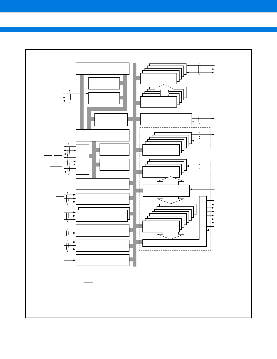
BLOCK DIAGRAM
* : INT23 to INT16 share pins with A23 to A16
* : INT15 shares pins with ATG
* : INT14 shares pins with DEOP2
* : INT13 to INT8 share pins with TRG5 to TRG0
* : INT7 to INT4 share pins with AIN0, BIN0, AIN1 and BIN1
The total number of above pins is 133. The remainder (144
-
133
=
11 pins) are V
CC
5 , V
CC
3 and V
SS
.
FR30 CPU
RAM 6 Kbyte
DMAC 8 ch
DREQ0 toDREQ
2
DACK0 toDACK
2
DEOP0 to
DEOP2
Resource Bus
Controller
Bus Converter
RAM 2 Kbyte
ROM 254 Kbyte
External Bus
Controller
A23 to A00
D31 to D16
RD
RDY
BRQ
BGRNT
CLK
WR1, WR0
Interrupt Controller
Clock Generator
Up/Down counter
◊
2 ch
24 ch external interrupt
10 bit 8 input A/D converter
level comparator
X0, X1, X0A, X1A
RST
MD0 to MD2
47
9
8
AIN0, 1
BIN0, 1
ZIN0, 1
INT0 to INT23 (
)
6
24
AN0 to AN7
AVRH, AVRL
AV
CC
, AV
SS
CMP (AN7)
12
15
5
6
6
SIN0 to SIN4
SOT0 to SOT4
SCK0 to SCK4
UART
◊
5 ch
Reload timer
◊
5 ch
8 bit 3 output D/A converter
DA0 toDA2
PPG0 to PPG5
TRG0 to TRG5
IN0 to IN3
FRCK
DAVC, DAVS
4
Multi-Function
Timer
16 bit PPG
◊
6 ch
16 bit ICU
◊
4 ch
16 bit FRT
16 bit OCU
◊
8 ch
Waveform Generator
RTO0 (U)
RTO1 (X)
RTO2 (V)
RTO3 (Y)
RTO4 (W)
RTO5 (Z)
RTO6
RTO7
DTTI
MB91133/MB91F133
23
s
CPU
1.
Memory Space
The FR series has 4 Gbytes (2
32
addresses) of logic address space which the CPU accesses linearly.
∑ Memory Map
* : It is impossible to access the external area on single-chip mode. When accessing the external area, select the
internal ROM external bus mode.
I/O
I/O
I/O
I/O
I/O
External ROM
external bus mode
Internal ROM
external bus mode
Single-chip mode
I/O
Access is
prohibited
Access is
prohibited
Access is
prohibited
Built-in RAM 6 KB
Built-in RAM 6 KB
Built-in RAM 6 KB
Access is
prohibited
Access is
prohibited
Access is
prohibited
External area
External area
External area
Built-in RAM 2KB
Built-in RAM 2KB
Built-in ROM
254KB
Built-in ROM
254KB
Access is
prohibited
Access is
prohibited
0000 0000
H
0000 0400
H
0000 0800
H
0000 1000
H
0000 2800
H
0001 0000
H
FFFF FFFF
H
010 0000
H
000C 0000
H
000C 0800
H
0001 0000
H
Refer to "I/O MAP"
Direct
Madressing
area
FFFF FFFF
H
MB91133/MB91F133
24
2.
Registers
There are two types of multi-purpose registers in the FR family. One is a dedicated purpose register that exists
within the CPU and the other is a multi-purpose register that exists in the memory.
∑ Dedicated Registers
∑ Program Status (PS)
PS is the register that holds the program status and is classified into three categories, namely, Condition Code
Register (CCR) , System Condition Code Register (SCR) and Interruption Level Master Register (ILM) .
Program Counter (PC)
: 32-bit length; indicates instruction storage position.
Program Status (PS)
: 32-bit length; stores register pointers and condition codes.
Table Base Register (TBR)
: Holds the starting address of the vector table to be used for Exception,
Interruption and Trapping (EIT) .
Return Pointer (RP)
: Holds the address to return to from the sub-routine.
System Stuck Pointer (SSP) : Indicates the system stuck position.
User Stuck Pointer (USP)
: Indicates the user's stuck position.
Multiplication and Division
Results Resister (MDH/MDL) : 32-bit length; act as registers for multiplication and division.
PC
PS
TBR
RP
SSP
USP
MDH
MDL
XXXX XXXX
H
Initial values
XXXX XXXX
H
XXXX XXXX
H
XXXX XXXX
H
XXXX XXXX
H
(Undecided)
(Undecided)
(Undecided)
(Undecided)
(Undecided)
0000 0000
H
000F FC00
H
Program Counter
Return Pointer
User Stuck Pointer
Program Status
Multiplication and
Division Results Resister
System Stuck Pointer
Table Base Register
32 bit
PS
ILM4 ILM3 ILM2
ILM
SCR
CCR
ILM1 ILM0
D1
D0
T
S
I
N
Z
V
C
0
1
2
3
4
5
6
7
8
9
10
16
17
18
19
20
31
MB91133/MB91F133
25
∑ Condition Code Register (CCR)
∑ System Condition Code Register (SCR)
∑ Interruption Level Mask Register (ILM)
S flag : Specifies the stuck pointer to be used as R15.
I flag
: Controls permission and prohibition of user interruption requests.
N flag : Indicates codes when computation results are defined as integers that are expressed in comple-
ments of 2.
Z flag : Indicates whether or not a result of the computation is "0" .
V flag : Operands used for computation are defined as integers expressed in complements of 2, and indi-
cate whether or not an overflow is generated as a result of the computation.
C flag : Indicates whether carrying or borrowing is generated from the highest bit as a result of the compu-
tation.
T flag : Specifies whether or not the step trace trap will be valid.
ILM4 to ILM0 : Holds the interruption level mask values, and those values that are held by the ILM are used
for the level mask. Interruption requests can be accepted only when the interruption levels
handled within the interruption requests to be input into the CPU are stronger than the levels
shown by the ILM.
ILM4
ILM3
ILM2
ILM1
ILM0
Interruption level
Strength
0
0
0
0
0
0
Strong
0
1
0
0
0
15
1
1
1
1
1
31
Weak
MB91133/MB91F133
26
s
MULTI-PURPOSE REGISTERS
The multi-purpose registers are CPU registers R0 to R15 which are used as accumulators for various compu-
tations and memory access pointers (fields that indicate the address) .
Special purposes are assumed for the following 3 of the 16 registers. Thus, some instructions are emphasized.
R13 : Virtual accumulator (AC)
R14 : Frame Pointer (FP)
R15 : Stack Pointer (SP)
Initial values for R0 to R14 on resetting are unspecified. The initial value of R15 will be 0000 0000
H
(SSP value) .
∑ Register bank configuration
R0
R1
R12
R13
R14
R15
AC (Accumulator)
32-bit
FP (Frame Pointer)
SP (Stack Pointer)
XXXX XXXX
H
Initial value
XXXX XXXX
H
0000 0000
H
MB91133/MB91F133
27
s
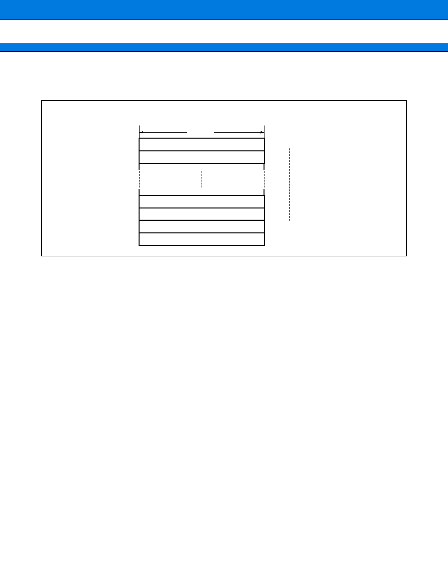
MODE SETTING
1.
Pins
∑ Mode pins and set mode
2.
Register
Mode register (MODR) and set mode
∑ Bus mode set bit and its functions
Mode pins
Mode name
Reset vector
access areas
External data
bus width
Bus modes
MD2
MD1
MD0
0
0
0
External vector mode 0
External
8-bit
External ROM external
bus mode
0
0
1
External vector mode 1
External
16-bit
0
1
0
Setting is prohibited
0
1
1
Internal vector mode
Internal
(Mode register) Single chip mode
1
Usage is prohibited
M1
M0
Functions
Remarks
0
0
Single chip mode
0
1
Internal ROM external bus mode
1
0
External ROM external bus mode
1
1
Setting is prohibited
Address
Initial value
Access
0000 07FF
H
XXXX XXXX
B
W
M1
M0
Bus mode set bit
*
*
*
*
*
*
W : Write only
X : Undecided
* : "0" should always be written for bits other than M1 and M0.
MB91133/MB91F133
28
s
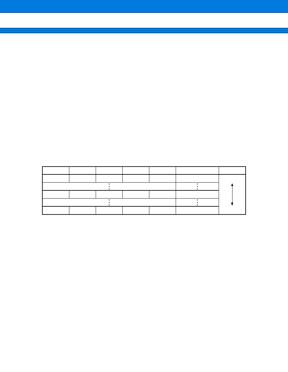
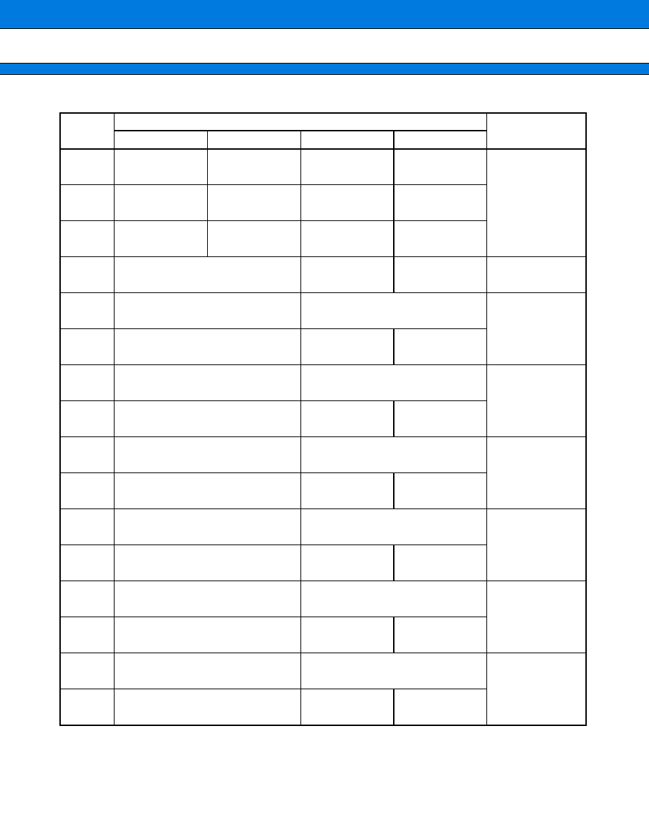
I/O MAP
(Continued)
Address
Register
Block
+
0
+
1
+
2
+
3
000000
H
PDR3
(R/W)
PDR2
(R/W)
Port Data
Register
XXXXXXXX
XXXXXXXX
000004
H
PDR6
(R/W)
PDR5
(R/W)
PDR4
(R/W)
XXXXXXXX
XXXXXXXX
XXXXXXXX
000008
H
PDR8
(R/W)
-
XXXXXXX
00000C
H
000010
H
PDRF
(R/W)
PDRE
(R/W)
PDRD
(R/W)
PDRC
(R/W)
XXXXXXXX
XXXXXXXX
XXXXXXXX
XXXXXXXX
000014
H
PDRJ
(R/W)
PDRI
(R/W)
PDRH
(R/W)
PDRG
(R/W)
-
-
XXXXXX
-
-
XXXXXX
-
-
-
-
-
XXX
-
-
XXXXXX
000018
H
LVLC
(R/W)
PDRL
(R/W)
PDRK
(R/W)
Level Comparator
XXXX
0
0
0
0
XXXXXXXX
XXXXXXXX
00001C
H
SSR0
(R/W)
SIDR0/SODR0 (R/W)
SCR0
(R/W)
SMR0
(R/W)
UART0
0 0 0 0 1 -
0
0
XXXXXXXX
0 0 0 0 0 1 0 0
0 0 0 0 0
-
0 0
000020
H
SSR1
(R/W)
SIDR1/SODR1 (R/W)
SCR1
(R/W)
SMR1
(R/W)
UART1
0 0 0 0 1 -
0
0
XXXXXXXX
0 0 0 0 0 1 0 0
0 0 0 0 0
-
0 0
000024
H
SSR2
(R/W)
SIDR2/SODR2 (R/W)
SCR2
(R/W)
SMR2
(R/W)
UART2
0 0 0 0 1 -
0
0
XXXXXXXX
0 0 0 0 0 1 0 0
0 0 0 0 0
-
0 0
000028
H
TMRLR
(W)
TMR
(R)
Reload Timer 0
XXXXXXXX XXXXXXXX
XXXXXXXX XXXXXXXX
00002C
H
TMCSR
(R/W)
-
-
-
-
0
0
0
0 0 0 0 0 0 0 0 0
000030
H
TMRLR
(W)
TMR
(R)
Reload Timer 1
XXXXXXXX XXXXXXXX
XXXXXXXX XXXXXXXX
000034
H
TMCSR
(R/W)
-
-
-
-
0
0
0
0 0 0 0 0 0 0 0 0
000038
H
ADCR
(R/W)
ADCS1
(R/W)
ADCS0
(R/W)
A/D Converter
(Sequential type)
0 0 1 0 1
-
XX XXXXXXXX
0 0 0 0 0 0 0 0
0 0 0 0 0 0 0 0
00003C
H
TMRLR
(W)
TMR
(R)
Reload Timer 2
XXXXXXXX XXXXXXXX
XXXXXXXX XXXXXXXX
000040
H
TMCSR
(R/W)
-
-
-
-
0
0
0
0 0 0 0 0 0 0 0 0
MB91133/MB91F133
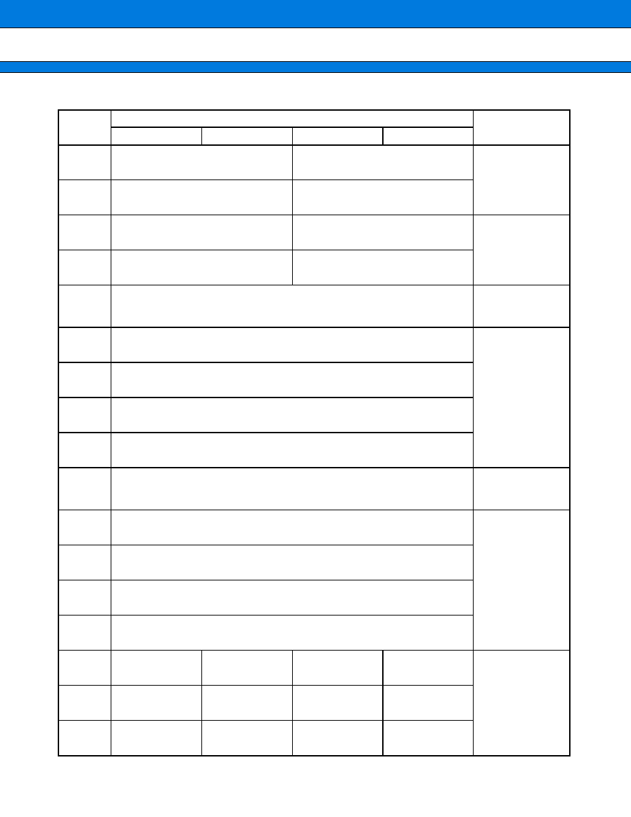
29
(Continued)
Address
Register
Block
+
0
+
1
+
2
+
3
000044
H
IPCP1
(R)
IPCP0
(R)
16-bit ICU
XXXXXXXX XXXXXXXX
XXXXXXXX XXXXXXXX
000048
H
IPCP3
(R)
IPCP2
(R)
XXXXXXXX XXXXXXXX
XXXXXXXX XXXXXXXX
00004C
H
ICS23
(R/W)
ICS01
(R/W)
0 0 0 0 0 0 0 0
0 0 0 0 0 0 0 0
000050
H
Reserved
000054
H
OCCP1
(R/W)
OCCP0
(R/W)
16-bit OCU
XXXXXXXX XXXXXXXX
XXXXXXXX XXXXXXXX
000058
H
OCCP3
(R/W)
OCCP2
(R/W)
XXXXXXXX XXXXXXXX
XXXXXXXX XXXXXXXX
00005C
H
OCCP5
(R/W)
OCCP4
(R/W)
XXXXXXXX XXXXXXXX
XXXXXXXX XXXXXXXX
000060
H
OCCP7
(R/W)
OCCP6
(R/W)
XXXXXXXX XXXXXXXX
XXXXXXXX XXXXXXXX
000064
H
OCS32
(R/W)
OCS10
(R/W)
XXX 0 0 0 0 0 0 0 0 0 XX 0 0
XXX 0 0 0 0 0 0 0 0 0 XX 0 0
000068
H
OCS76
(R/W)
OCS54
(R/W)
XXX 0 0 0 0 0 0 0 0 0 XX 0 0
XXX 0 0 0 0 0 0 0 0 0 XX 0 0
00006C
H
TCDT
(R/W)
TCCS
(R/W)
16-bit
Free-run Timer
0 0 0 0 0 0 0 0 0 0 0 0 0 0 0 0
0
-
-
-
-
-
-
- 0 0 0 0 0 0 0 0
000070
H
SSR3
(R/W)
SIDR3/SODR3 (R/W)
SCR3
(R/W)
SMR3
(R/W)
UART3
0 0 0 0 1 0 0
0
XXXXXXXX
0 0 0 0 0 1 0 0
0 0 0 0 0
-
0 0
000074
H
SSR4
(R/W)
SIDR4/SODR4 (R/W)
SCR4
(R/W)
SMR4
(R/W)
UART4
0 0 0 0 1 0 0
0
XXXXXXXX
0 0 0 0 0 1 0 0
0 0 0 0 0
-
0 0
000078
H
CDCR1
(R/W)
CDCR0
(R/W)
Communication
Pre-scalar
0 -
-
-
0 0 0 0
0 -
-
-
0 0 0 0
00007C
H
CDCR3
(R/W)
CDCR2
(R/W)
0 -
-
-
0 0 0 0
0 -
-
-
0 0 0 0
000080
H
CDCR4
(R/W)
0 -
-
-
0 0 0 0
MB91133/MB91F133
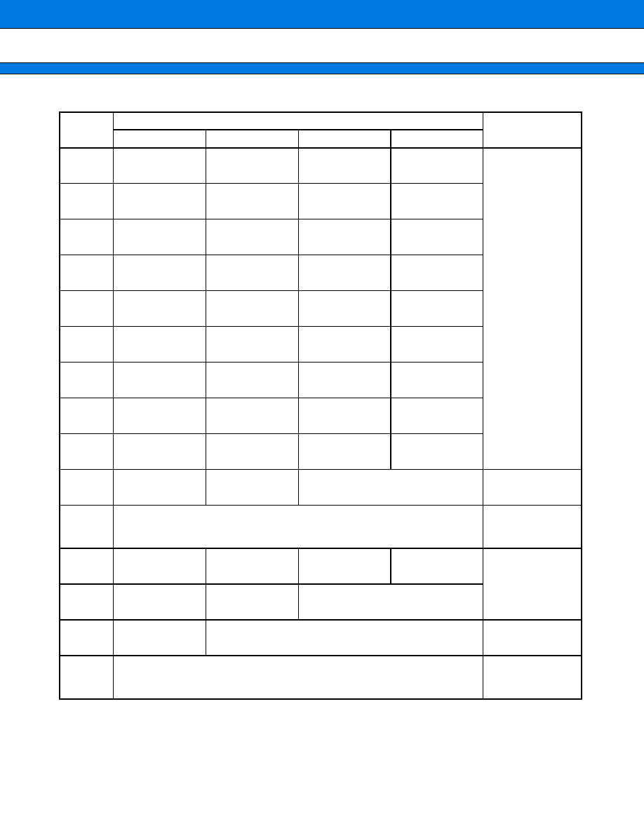
30
(Continued)
Address
Register
Block
+
0
+
1
+
2
+
3
000084
H
RCR1
(W)
RCR0
(W)
UDCR1
(R)
UDCR0
(R)
8-/16-bit
U/D Counter
0 0 0 0 0 0 0 0
0 0 0 0 0 0 0 0
0 0 0 0 0 0 0 0
0 0 0 0 0 0 0 0
000088
H
CCRH0
(R/W)
CCRL0
(R/W)
CSR0
(R/W)
0 0 0 0 0 0 0 0
-
0 0 0 1 0 0 0
0 0 0 0 0 0 0 0
00008C
H
CCRH1
(R/W)
CCRL1
(R/W)
CSR1
(R/W)
-
0 0 0 0 0 0 0
-
0 0 0 1 0 0 0
0 0 0 0 0 0 0 0
000090
H
Reserved
000094
H
EIRR0
(R/W)
ENIR0
(R/W)
EIRR1
(R/W)
ENIR1
(R/W)
Ext Int
0 0 0 0 0 0 0 0
0 0 0 0 0 0 0 0
0 0 0 0 0 0 0 0
0 0 0 0 0 0 0 0
000098
H
ELVR0
(R/W)
ELVR1
(R/W)
0 0 0 0 0 0 0 0 0 0 0 0 0 0 0 0
0 0 0 0 0 0 0 0 0 0 0 0 0 0 0 0
00009C
H
EIRR2
(R/W)
ENIR2
(R/W)
0 0 0 0 0 0 0 0
0 0 0 0 0 0 0 0
0000A0
H
ELVR2
(R/W)
0 0 0 0 0 0 0 0 0 0 0 0 0 0 0 0
0000A4
H
DACR2
(R/W)
DACR1
(R/W)
DACR0
(R/W)
D/A Converter
-
-
-
-
-
-
-
0
-
-
-
-
-
-
-
0
-
-
-
-
-
-
-
0
0000A8
H
DADR2
(R/W)
DADR1
(R/W)
DADR0
(R/W)
XXXXXXXX
XXXXXXXX
XXXXXXXX
0000AC
H
DTCR1
(R/W)
TMRR1
(R/W)
DTCR0
(R/W)
TMRR0
(R/W)
Waveform
Generator
0 0 0 0 0 0 0 0
XXXXXXXX
0 0 0 0 0 0 0 0
XXXXXXXX
0000B0
H
SIGCR
(R/W)
DTCR2
(R/W)
TMRR2
(R/W)
0 0 0 0 0 0 0 0
0 0 0 0 0 0 0 0
XXXXXXXX
0000B4
H
to
0000BC
H
Reserved
0000C0
H
PCRE
(R/W)
PCRD
(R/W)
PCRC
(R/W)
Pull-up Control
-
-
-
-
-
-
0 0
0 0 0 0 0 0 0 0
0 0 0 0 0 0 0 0
0000C4
H
PCRJ
(R/W)
PCRI
(R/W)
PCRH
(R/W)
-
-
0 0 0 0 0 0
-
-
0 0 0 0 0 0
-
-
-
-
-
0 0 0
0000C8
H
OCRJ
(R/W)
OCRI
(R/W)
OCRH
(R/W)
Open-drain Control
-
-
0 0 0 0 0 0
-
-
0 0 0 0 0 0
-
-
-
-
-
0 0 0
0000CC
H
AICK
(R/W)
Analog
Input Control
0 0 0 0 0 0 0 0
MB91133/MB91F133
31
(Continued)
Address
Register
Block
+
0
+
1
+
2
+
3
0000D0
H
DDRF
(R/W)
DDRE
(R/W)
DDRD
(R/W)
DDRC
(R/W)
Data Direction
Register
0 0 0 0 0 0 0 0
0 0 0 0 0 0 0 0
0 0 0 0 0 0 0 0
0 0 0 0 0 0 0 0
0000D4
H
DDRJ
(R/W)
DDRI
(R/W)
DDRH
(R/W)
DDRG
(R/W)
-
-
0 0 0 0 0 0
-
-
0 0 0 0 0 0
-
-
-
-
-
0 0 0
-
-
0 0 0 0 0 0
0000D8
H
DDRL
(R/W)
DDRK
(R/W)
0 0 0 0 0 0 0 0
0 0 0 0 0 0 0 0
0000DC
H
GCN1
(R/W)
GCN2
(R/W)
PPG ctl
0 0 1 1 0 0 1 0 0 0 0 1 0 0 0 0
0 0 0 0 0 0 0 0
0000E0
H
PTMR0
(R)
PCSR0
(W)
PPG0
1 1 1 1 1 1 1 1 1 1 1 1 1 1 1 1
XXXXXXXX XXXXXXXX
0000E4
H
PDUT0
(W)
PCNH0
(R/W)
PCNL0
(R/W)
XXXXXXXX XXXXXXXX
0 0 0 0 0 0 0 -
0 0 0 0 0 0 0 0
0000E8
H
PTMR1
(R)
PCSR1
(W)
PPG1
1 1 1 1 1 1 1 1 1 1 1 1 1 1 1 1
XXXXXXXX XXXXXXXX
0000EC
H
PDUT1
(W)
PCNH1
(R/W)
PCNL1
(R/W)
XXXXXXXX XXXXXXXX
0 0 0 0 0 0 0 -
0 0 0 0 0 0 0 0
0000F0
H
PTMR2
(R)
PCSR2
(W)
PPG2
1 1 1 1 1 1 1 1 1 1 1 1 1 1 1 1
XXXXXXXX XXXXXXXX
0000F4
H
PDUT2
(W)
PCNH2
(R/W)
PCNL2
(R/W)
XXXXXXXX XXXXXXXX
0 0 0 0 0 0 0 -
0 0 0 0 0 0 0 0
0000F8
H
PTMR3
(R)
PCSR3
(W)
PPG3
1 1 1 1 1 1 1 1 1 1 1 1 1 1 1 1
XXXXXXXX XXXXXXXX
0000FC
H
PDUT3
(W)
PCNH3
(R/W)
PCNL3
(R/W)
XXXXXXXX XXXXXXXX
0 0 0 0 0 0 0 -
0 0 0 0 0 0 0 0
000100
H
PTMR4
(R)
PCSR4
(W)
PPG4
1 1 1 1 1 1 1 1 1 1 1 1 1 1 1 1
XXXXXXXX XXXXXXXX
000104
H
PDUT4
(W)
PCNH4
(R/W)
PCNL4
(R/W)
XXXXXXXX XXXXXXXX
0 0 0 0 0 0 0 -
0 0 0 0 0 0 0 0
000108
H
PTMR5
(R)
PCSR5
(W)
PPG5
1 1 1 1 1 1 1 1 1 1 1 1 1 1 1 1
XXXXXXXX XXXXXXXX
00010C
H
PDUT5
(W)
PCNH5
(R/W)
PCNL5
(R/W)
XXXXXXXX XXXXXXXX
0 0 0 0 0 0 0 -
0 0 0 0 0 0 0 0
MB91133/MB91F133
32
(Continued)
Address
Register
Block
+
0
+
1
+
2
+
3
000110
H
TMRLR
(W)
TMR
(R)
Reload Timer 3
XXXXXXXX XXXXXXXX
XXXXXXXX XXXXXXXX
000114
H
TMCSR
(R/W)
-
-
-
-
0
0
0
0 0 0 0 0 0 0 0 0
000118
H
TMRLR
(W)
TMR
(R)
Reload Timer 4
XXXXXXXX XXXXXXXX
XXXXXXXX XXXXXXXX
00011C
H
TMCSR
(R/W)
-
-
-
-
0
0
0
0 0 0 0 0 0 0 0 0
000120
H
to
0001FC
H
Reserved
000200
H
DPDP
(R/W)
DMAC
-
-
-
-
-
-
-
-
-
-
-
-
-
-
-
-
-
-
-
-
-
-
-
-
-
0 0 0 0 0 0 0
000204
H
DACSR
(R/W)
0 0 0 0 0 0 0 0
0 0 0 0 0 0 0 0
0 0 0 0 0 0 0 0
0 0 0 0 0 0 0 0
000208
H
DATCR
(R/W)
XXXXXXXX
XXXX0 0 0 0
XXXX0 0 0 0
XXXX0 0 0 0
00020C
H
000210
H
to
0003EC
H
Reserved
0003F0
H
BSD0
(W)
Bit Search Module
XXXXXXXX
XXXXXXXX
XXXXXXXX
XXXXXXXX
0003E4
H
BSD1
(R/W)
XXXXXXXX
XXXXXXXX
XXXXXXXX
XXXXXXXX
0003F8
H
BSDC
(W)
XXXXXXXX
XXXXXXXX
XXXXXXXX
XXXXXXXX
0003FC
H
BSRR
(R)
XXXXXXXX
XXXXXXXX
XXXXXXXX
XXXXXXXX
000400
H
ICR00
(R/W)
ICR01
(R/W)
ICR02
(R/W)
ICR03
(R/W)
Interrupt Control
Unit
-
-
-
-
1 1 1 1
-
-
-
-
1 1 1 1
-
-
-
-
1 1 1 1
-
-
-
-
1 1 1 1
000404
H
ICR04
(R/W)
ICR05
(R/W)
ICR06
(R/W)
ICR07
(R/W)
-
-
-
-
1 1 1 1
-
-
-
-
1 1 1 1
-
-
-
-
1 1 1 1
-
-
-
-
1 1 1 1
000408
H
ICR08
(R/W)
ICR09
(R/W)
ICR10
(R/W)
ICR11
(R/W)
-
-
-
-
1 1 1 1
-
-
-
-
1 1 1 1
-
-
-
-
1 1 1 1
-
-
-
-
1 1 1 1
MB91133/MB91F133
33
(Continued)
Address
Register
Block
+
0
+
1
+
2
+
3
00040C
H
ICR12
(R/W)
ICR13
(R/W)
ICR14
(R/W)
ICR15
(R/W)
Interrupt Control
Unit
-
-
-
-
1 1 1 1
-
-
-
-
1 1 1 1
-
-
-
-
1 1 1 1
-
-
-
-
1 1 1 1
000410
H
ICR16
(R/W)
ICR17
(R/W)
ICR18
(R/W)
ICR19
(R/W)
-
-
-
-
1 1 1 1
-
-
-
-
1 1 1 1
-
-
-
-
1 1 1 1
-
-
-
-
1 1 1 1
000414
H
ICR20
(R/W)
ICR21
(R/W)
ICR22
(R/W)
ICR23
(R/W)
-
-
-
-
1 1 1 1
-
-
-
-
1 1 1 1
-
-
-
-
1 1 1 1
-
-
-
-
1 1 1 1
000418
H
ICR24
(R/W)
ICR25
(R/W)
ICR26
(R/W)
ICR27
(R/W)
-
-
-
-
1 1 1 1
-
-
-
-
1 1 1 1
-
-
-
-
1 1 1 1
-
-
-
-
1 1 1 1
00041C
H
ICR28
(R/W)
ICR29
(R/W)
ICR30
(R/W)
ICR31
(R/W)
-
-
-
-
1 1 1 1
-
-
-
-
1 1 1 1
-
-
-
-
1 1 1 1
-
-
-
-
1 1 1 1
000420
H
ICR32
(R/W)
ICR33
(R/W)
ICR34
(R/W)
ICR35
(R/W)
-
-
-
-
1 1 1 1
-
-
-
-
1 1 1 1
-
-
-
-
1 1 1 1
-
-
-
-
1 1 1 1
000424
H
ICR36
(R/W)
ICR37
(R/W)
ICR38
(R/W)
ICR39
(R/W)
-
-
-
-
1 1 1 1
-
-
-
-
1 1 1 1
-
-
-
-
1 1 1 1
-
-
-
-
1 1 1 1
000428
H
ICR40
(R/W)
ICR41
(R/W)
ICR42
(R/W)
ICR43
(R/W)
-
-
-
-
1 1 1 1
-
-
-
-
1 1 1 1
-
-
-
-
1 1 1 1
-
-
-
-
1 1 1 1
00042C
H
ICR44
(R/W)
ICR45
(R/W)
ICR46
(R/W)
ICR47
(R/W)
-
-
-
-
1 1 1 1
-
-
-
-
1 1 1 1
-
-
-
-
1 1 1 1
-
-
-
-
1 1 1 1
000430
H
DICR
(R/W)
HRCL
(R/W)
Delay Int
-
-
-
-
-
-
-
0
-
-
-
1 1 1 1 1
000434
H
to
00047C
H
Reserved
000480
H
RSRR/WTCR (R/W)
STCR
(R/W)
PDRR
(R/W)
CTBR
(W)
Clock Control Unit
1 XXXX
-
0 0
0 0 0 1 1 1
-
-
-
-
-
-
0 0 0 0
XXXXXXXX
000484
H
GCR
(R/W)
WPR
(W)
1 1 0 0 1 1
-
1
XXXXXXXX
000488
H
CT
(R/W)
PLL Control
0 0
-
-
0
-
0 0
00048C
H
to
0005FC
H
Reserved
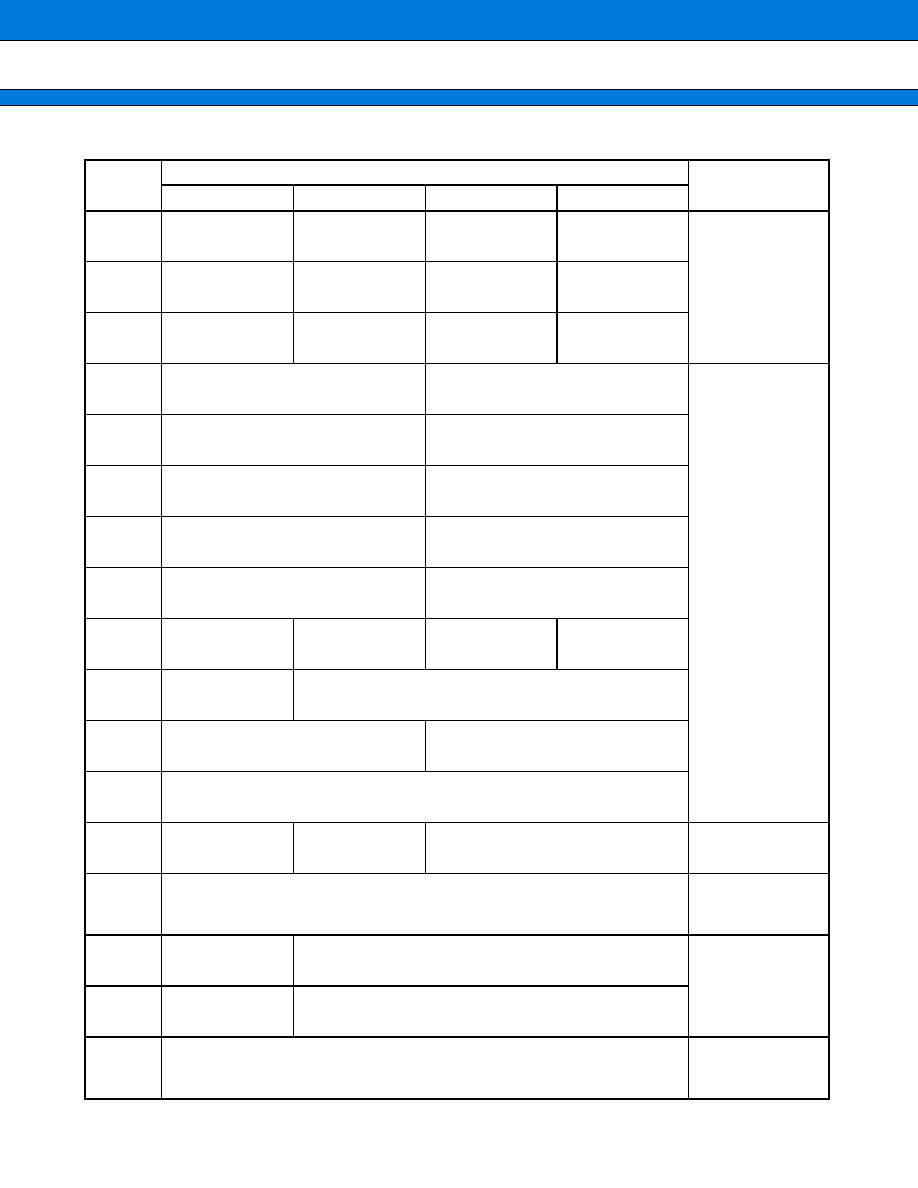
MB91133/MB91F133
34
(Continued)
Address
Register
Block
+
0
+
1
+
2
+
3
000600
H
DDR3
(W)
DDR2
(W)
Data Direction
Register
0 0 0 0 0 0 0 0
0 0 0 0 0 0 0 0
000604
H
DDR6
(W)
DDR5
(W)
DDR4
(W)
0 0 0 0 0 0 0 0
0 0 0 0 0 0 0 0
0 0 0 0 0 0 0 0
000608
H
DDR8
(W)
-
0 0 0 0 0 0 0
00060C
H
ASR1
(W)
AMR1
(W)
T-unit
0 0 0 0 0 0 0 0 0 0 0 0 0 0 0 1
0 0 0 0 0 0 0 0 0 0 0 0 0 0 0 0
000610
H
ASR2
(W)
AMR2
(W)
0 0 0 0 0 0 0 0 0 0 0 0 0 0 1 0
0 0 0 0 0 0 0 0 0 0 0 0 0 0 0 0
000614
H
ASR3
(W)
AMR3
(W)
0 0 0 0 0 0 0 0 0 0 0 0 0 0 1 1
0 0 0 0 0 0 0 0 0 0 0 0 0 0 0 0
000618
H
ASR4
(W)
AMR4
(W)
0 0 0 0 0 0 0 0 0 0 0 0 0 1 0 0
0 0 0 0 0 0 0 0 0 0 0 0 0 0 0 0
00061C
H
ASR5
(W)
AMR5
(W)
0 0 0 0 0 0 0 0 0 0 0 0 0 1 0 1
0 0 0 0 0 0 0 0 0 0 0 0 0 0 0 0
000620
H
AMD0
(R/W)
AMD1
(R/W)
AMD32
(R/W)
AMD4
(R/W)
-
-
-
0 0 1 1 1
0
-
-
0 0 0 0 0
0 0 0 0 0 0 0 0
0
-
-
0 0 0 0 0
000624
H
AMD5
(R/W)
0
-
-
0 0 0 0 0
000628
H
EPCR0
(W)
EPCR1
(W)
-
-
-
-
1 1 0 0 -
1
-
-
-
-
-
-
-
-
-
-
-
-
-
- 1 1 1 1 1 1 1 1
00062C
H
000630
H
PCR6
(R/W)
Pull-up Control
0 0 0 0 0 0 0 0
000634
H
to
0007BC
H
Reserved
0007C0
H
FLCR
(R/W)
FLASH Control
0 0 0 X 0 0 0 0
0007C4
H
FWTC
(R/W)
-
-
-
-
-
0 0 0
0007C8
H
to
0007F8
H
Reserved

MB91133/MB91F133
35
(Continued)
*1 : Do not execute RMW instructions to registers with write-only bits.
*2 : Do not execute write access to read-only or reserved registers except for particular requests.
*3 : Data in areas with "-" or reserved ones are unspecified.
*4 : RMW instructions (RMW : Read / Modify / Write)
Address
Register
Block
+
0
+
1
+
2
+
3
0007FC
H
LER
(W)
MODR
(W)
Little Endian
Register
Mode Register
-
-
-
-
-
0 0 0
XXXXXXXX
AND
Rj, @Ri
OR
Rj, @Ri
EOR
Rj, @Ri
ANDH
Rj, @Ri
ORH
Rj, @Ri
EORH
Rj, @Ri
ANDB
Rj, @Ri
ORB
Rj, @Ri
EORB
Rj, @Ri
BANDL #u4, @Ri
BORL #u4, @Ri
BEORL #u4, @Ri
BANDH #u4, @Ri
BORH #u4, @Ri
BEORH #u4, @Ri
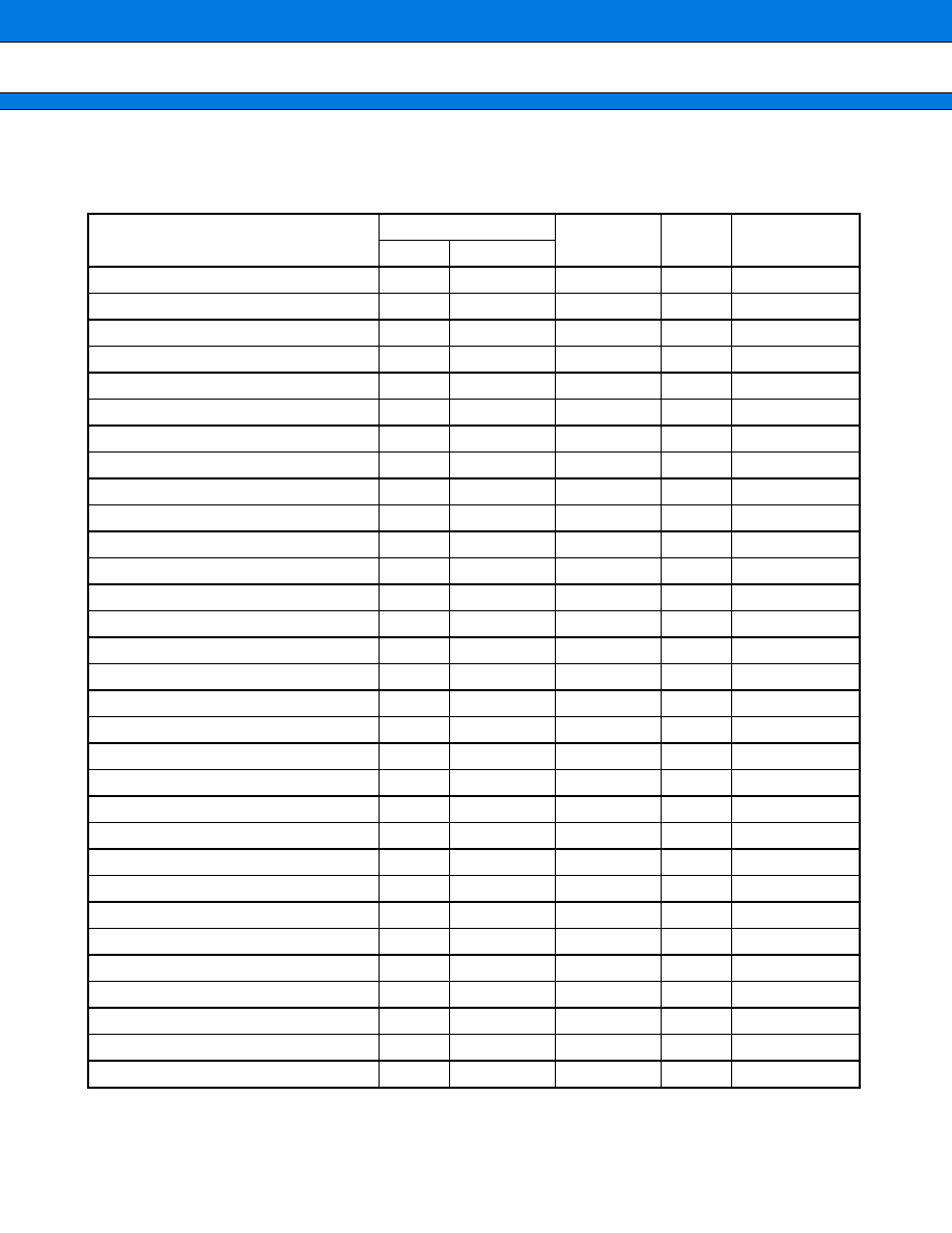
MB91133/MB91F133
36
s
INTERRUPTION VECTOR
Causes of MB91130 interruptions and allocation of interruption vectors and interruption control registers are
described in the interruption vector table.
(Continued)
Interruption sauce
Interruption number
Interruption
level
*1
Offset
Address
*2
of TBR default
Decimal Hexadecimal
Reset
0
00
3FC
H
000FFFFC
H
System reservation
1
01
3F8
H
000FFFF8
H
System reservation
2
02
3F4
H
000FFFF4
H
System reservation
3
03
3F0
H
000FFFF0
H
System reservation
4
04
3EC
H
000FFFEC
H
System reservation
5
05
3E8
H
000FFFE8
H
System reservation
6
06
3E4
H
000FFFE4
H
System reservation
7
07
3E0
H
000FFFE0
H
System reservation
8
08
3DC
H
000FFFDC
H
System reservation
9
09
3D8
H
000FFFD8
H
System reservation
10
0A
3D4
H
000FFFD4
H
System reservation
11
0B
3D0
H
000FFFD0
H
System reservation
12
0C
3CC
H
000FFFCC
H
System reservation
13
0D
3C8
H
000FFFC8
H
Exceptions to undefined instructions
14
0E
3C4
H
000FFFC4
H
System reservation
15
0F
3C0
H
000FFFC0
H
External interruption 0
16
10
ICR00
3BC
H
000FFFBC
H
External interruption 1
17
11
ICR01
3B8
H
000FFFB8
H
External interruption 2
18
12
ICR02
3B4
H
000FFFB4
H
External interruption 3
19
13
ICR03
3B0
H
000FFFB0
H
External interruption 4
20
14
ICR04
3AC
H
000FFFAC
H
External interruption 5
21
15
ICR05
3A8
H
000FFFA8
H
External interruption 6
22
16
ICR06
3A4
H
000FFFA4
H
External interruption 7
23
17
ICR07
3A0
H
000FFFA0
H
External interruption 8 to 15
24
18
ICR08
39C
H
000FFF9C
H
External interruption 16 to 23
25
19
ICR09
398
H
000FFF98
H
UART0 (Reception completion)
26
1A
ICR10
394
H
000FFF94
H
UART1 (Reception completion)
27
1B
ICR11
390
H
000FFF90
H
UART2 (Reception completion)
28
1C
ICR12
38C
H
000FFF8C
H
UART3 (Reception completion)
29
1D
ICR13
388
H
000FFF88
H
UART4 (Reception completion)
30
1E
ICR14
384
H
000FFF84
H
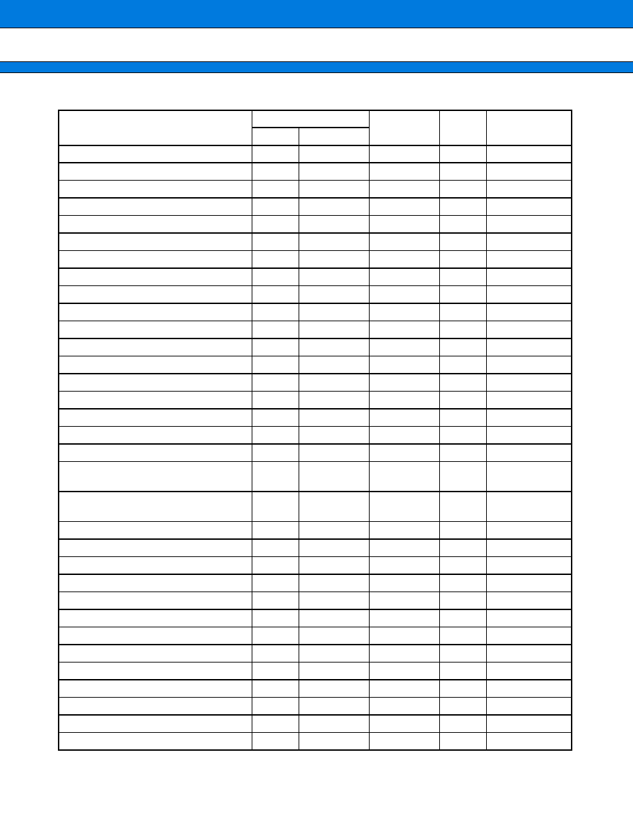
MB91133/MB91F133
37
(Continued)
Interruption sauce
Interruption number
Interruption
level
*1
Offset
Address
*2
of TBR default
Decimal Hexadecimal
UART0 (Transmission completion)
31
1F
ICR15
380
H
000FFF80
H
UART1 (Transmission completion)
32
20
ICR16
37C
H
000FFF7C
H
UART2 (Transmission completion)
33
21
ICR17
378
H
000FFF78
H
UART3 (Transmission completion)
34
22
ICR18
374
H
000FFF74
H
UART4 (Transmission completion)
35
23
ICR19
370
H
000FFF70
H
DMAC (end, error)
36
24
ICR20
36C
H
000FFF6C
H
Reload timer 0
37
25
ICR21
368
H
000FFF68
H
Reload timer 1
38
26
ICR22
364
H
000FFF64
H
Reload timer 2
39
27
ICR23
360
H
000FFF60
H
Reload timer 3
40
28
ICR24
35C
H
000FFF5C
H
Reload timer 4
41
29
ICR25
358
H
000FFF58
H
A/D (sequential type)
42
2A
ICR26
354
H
000FFF54
H
PPG0
43
2B
ICR27
350
H
000FFF50
H
PPG1
44
2C
ICR28
34C
H
000FFF4C
H
PPG2
45
2D
ICR29
348
H
000FFF48
H
PPG3
46
2E
ICR30
344
H
000FFF44
H
PPG4/5
47
2F
ICR31
340
H
000FFF40
H
Waveform generator
48
30
ICR32
33C
H
000FFF3C
H
U/D counter 0 (compare/
underflow-overflow, up/down invert)
49
31
ICR33
338
H
000FFF38
H
U/D counter 1 (compare/
underflow-overflow, up/down invert)
50
32
ICR34
334
H
000FFF34
H
ICU0 (load)
51
33
ICR35
330
H
000FFF30
H
ICU1 (load)
52
34
ICR36
32C
H
000FFF2C
H
ICU2 (load)
53
35
ICR37
328
H
000FFF28
H
ICU3 (load)
54
36
ICR38
324
H
000FFF24
H
OCU0 (matched)
55
37
ICR39
320
H
000FFF20
H
OCU1 (matched)
56
38
ICR40
31C
H
000FFF1C
H
OCU2 (matched)
57
39
ICR41
318
H
000FFF18
H
OCU3 (matched)
58
3A
ICR42
314
H
000FFF14
OCU4/5 (matched)
59
3B
ICR43
310
H
000FFF10
H
OCU6/7 (matched)
60
3C
ICR44
30C
H
000FFF0C
H
Level comparator
61
3D
ICR45
308
H
000FFF08
H
16-bit freerun timer
62
3E
ICR46
304
H
000FFF04
H
Delay interruption factor bit
63
3F
ICR47
300
H
000FFF00
H
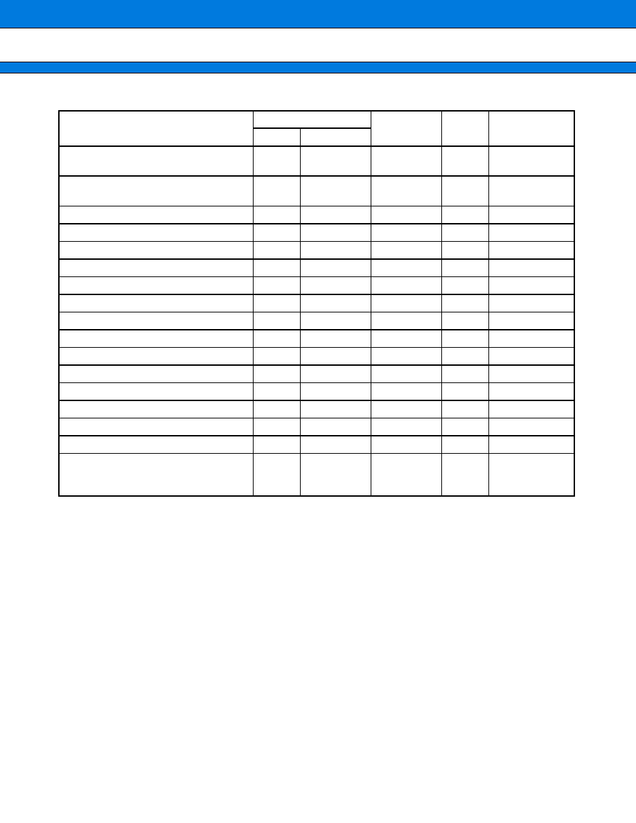
MB91133/MB91F133
38
(Continued)
*1 : ICR sets the interruption level for each interruption request using the register built into the interruption controller.
ICR is prepared in accordance with each interruption request.
*2 : TBR is the register that indicates the starting address of the vector table for EIT.
Addresses with added offset values that are specified per TBR and EIT factor will be the vector addresses.
*3 : 0X40, 0X41 interruptions for system codes are used in the event that REALOS/FR is used.
Interruption sauce
Interruption number
Interruption
level
*1
Offset
Address
*2
of TBR default
Decimal Hexadecimal
System reservation
(used under REALOS
*3
)
64
40
2FC
H
000FFEFC
H
System reservation
(used under REALOS
*3
)
65
41
2F8
H
000FFEF8
H
Used under INT instruction
66
42
2F4
H
000FFEF4
H
Used under INT instruction
67
43
2F0
H
000FFEF0
H
Used under INT instruction
68
44
2EC
H
000FFEEC
H
Used under INT instruction
69
45
2E8
H
000FFEE8
H
Used under INT instruction
70
46
2E4
H
000FFEE4
H
Used under INT instruction
71
47
2E0
H
000FFEE0
H
Used under INT instruction
72
48
2DC
H
000FFEDC
H
Used under INT instruction
73
49
2D8
H
000FFED8
H
Used under INT instruction
74
4A
2D4
H
000FFED4
H
Used under INT instruction
75
4B
2D0
H
000FFED0
H
Used under INT instruction
76
4C
2CC
H
000FFECC
H
Used under INT instruction
77
4D
2C8
H
000FFEC8
H
Used under INT instruction
78
4E
2C4
H
000FFEC4
H
Used under INT instruction
79
4F
2C0
H
000FFEC0
H
Used under INT instruction
80
to
255
50
to
FF
2BC
H
to
000
H
000FFEBC
H
to
000FFC00
H
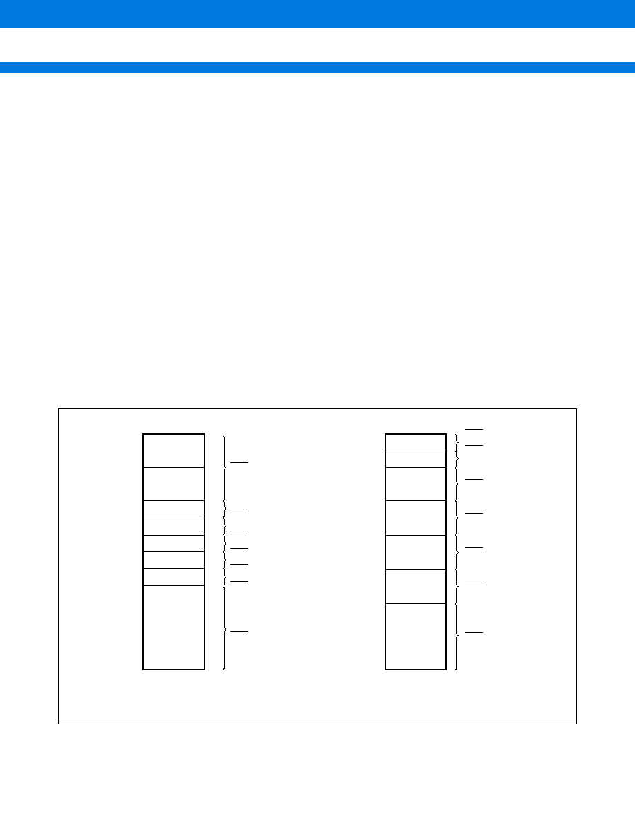
MB91133/MB91F133
39
s
PERIPHERAL RESOURCES
1.
Bus Interface
The bus interface controls the interface with external memory and external I/O.
∑ Bus Interface Characteristics
∑ 24-bit (16 MB) address output
∑ 16/8-bit bus width can be set.
∑ Insertion of programmable "automatic memory wait" (maximum of 7 cycles)
∑ Supports "little endian" mode
∑ Unused addresses / data pins can be used as I/O ports.
∑ Clock doubled should be used if the external bus exceeds 25 MHz. Bus speed is 1/2 of the CPU speed.
∑ Areas
A total of six types of chip selection areas are prepared for the bus interface. The position of each area can be
randomly arranged per 64 KB at least using area selection registers (ASR1 to ASR 5) and area mask registers
(AMR1 to AMR 5) in an area of 4 GB. The area 0 is allocated to space outside the area specified by ASR1 to
ASR5. External areas other than 00010000
H
to 0005FFFF
H
are deemed area 0 on resetting.
There is no chip selection output pin so no setting is required. Setting it has no effect on usage.
Figure 4.1-1 shows an example in which areas 1 to 5 are arranged from 00100000
H
to 0014FFFF
H
in 64 KB
units. Also, Figure 4.1-2 shows an example in which area 1 is arranged as 00000000
H
to 0007FFFF
H
in 512 KB
and areas 2 to 5 are arranged as 00100000
H
to 004FFFFF
H
in 1-MB units.
00000000
H
00000000
H
00080000
H
000FFFFF
H
001FFFFF
H
002FFFFF
H
003FFFFF
H
004FFFFF
H
00080000
H
000FFFFF
H
0010FFFF
H
0011FFFF
H
0012FFFF
H
0013FFFF
H
0014FFFF
H
CS0 (1 Mbyte)
CS1 (512 K)
CS0 (512 K)
CS2 (1 Mbyte)
CS3 (1 Mbyte)
CS4 (1 Mbyte)
CS5 (1 Mbyte)
CS0
CS0
CS1 (64 Kbyte)
CS2 (64 Kbyte)
CS3 (64 Kbyte)
CS4 (64 Kbyte)
CS5 (64 Kbyte)
Figure 4.1-1
Area Arrangement Example 1
Figure 4.1-2
Area Arrangement Example 2
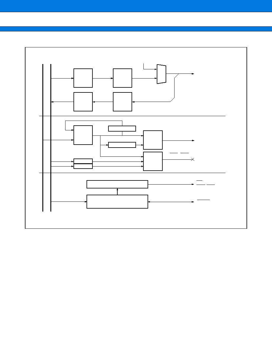
MB91133/MB91F133
40
∑ Block Diagram
write
buffer
read
buffer
address
buffer
switch
switch
A - Out
M
U
X
External
DATA Bus
ASR
AMR
registers
&
Control
shifter
compa-
rator
inpage
External pin control area
+
1 or
+
2
DATA BLOCK
ADDRESS BLOCK
External
Address Bus
CS0 - CS5
Controls all blocks
RD
WR0. WR1
BRQ
BGRNT
RDY
ADDRESS B
U
S
D
ATA
B
U
S
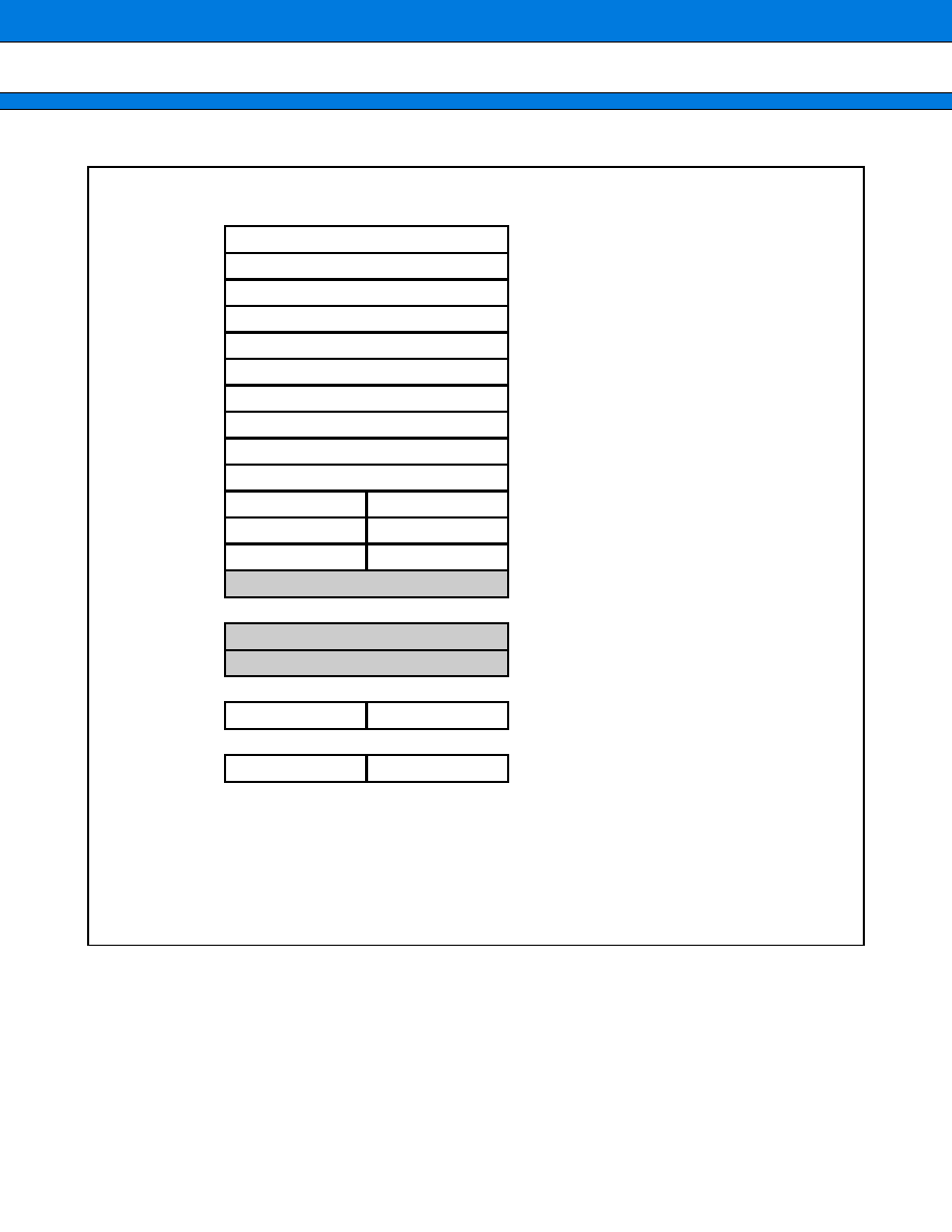
MB91133/MB91F133
41
∑ Register List
0000060C
H
0000060E
H
00000610
H
00000612
H
00000614
H
00000616
H
00000618
H
0000061A
H
0000061C
H
0000061E
H
00000620
H
00000622
H
00000624
H
00000626
H
0000062C
H
0000062E
H
00000688
H
000007FE
H
ASR1
Area Select Register 1
Area Mask Register 1
Area Select Register 2
Area Mask Register 2
Area Select Register 3
Area Mask Register 3
Area Select Register 4
Area Mask Register 4
Area Select Register 5
Area Mask Register 5
Area Mode Register 0 / Area Mode Register 1
Area Mode Register 32 / Area Mode Register 4
Area Mode Register 5
ReFresh Control Register
DRAM Control Register 4
DRAM Control Register 4
External Pin Control Register
Little Endian Register / MODe Register
AMR1
ASR2
AMR2
ASR3
AMR3
ASR4
AMR4
ASR5
AMR5
RFCR
DMCR5
DMCR4
EPCR0
EPCR1
LER
MODR
AMD5
AMD0
AMD1
AMD32
AMD4
15
Address
8
7
0
Note : Functional pins have not been prepared in the shaded area for MB91133/MB91F133, so these
registers should not be accessed.
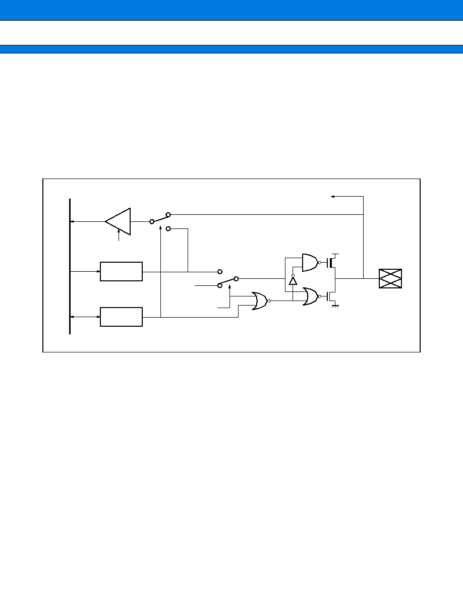
MB91133/MB91F133
42
2.
I/O Port
MB91133/MB91F133 can be used as an I/O port when the setting for resources dealing with each pin does not
use the pin for input/output.
As regards the read value of the port (PDR) , the pin level is read out when input is set for the port. If output is
set, the data register value is read out. This is the same for reading under Read Modify Write.
If the input setting is changed to output setting, output data should be set first. If Read Modify Write instructions
(i.e. bit set) are used in this case, the data that is read out is the input data from the pin and is not the latch value
of the data register, so care must be taken.
∑ Basic I/O Port Block Diagram
∑ I/O Port Register
The I/O port consists of the Port Data Register (PDR) and Port Direction Register (DDR) .
∑ In case of input mode (DDR
=
"0")
When PDR reads : Level of external pins handled is read out.
When PDR writes : Set value is written in PDR.
∑ In case of output mode (DDR
=
"1")
When PDR reads : PDR values are read out.
When PDR writes : PDR values are output to the external pin handled.
∑ Switching control for resources and ports of the analog pin (A/D)
∑ Resources and ports of the analog pin (A/D) are switched using the Analog Input Control register on Port K
(AICK) .
This controls whether Port K is used as an analog or general-purpose port.
0 : General-purpose port
1 : Analog input (A/D)
Data bus
PDR read
Resource input
Resource output
Resource output
permission
0
1
0
1
pin
PDR
DDR
PDR : Port Data Register
DDR : Data Direction Register
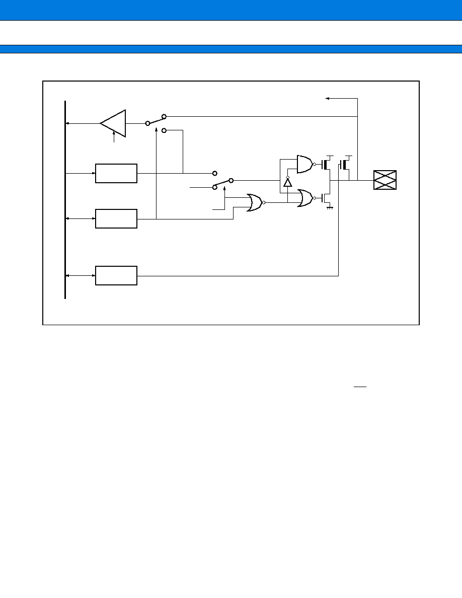
MB91133/MB91F133
43
∑ Block Diagram of Input/Output Port (with Pull-up Resistance)
∑ Pull-up resistance control register (PCR) R/W
Turns pull-up resistance ON/OFF.
0 : Pull-up resistance turned off
1 : Pull-up resistance turned on
Notes :
∑
The pull-up resistance control register setting is handled as a priority in stop mode (HIZ
=
1) as well.
∑
Use of the pull-up resistance control function is prohibited when the pin concerned is used as the external
bus pin. "1" should not be written in this register.
Data bus
PDR read
0
1
0
1
pin
PDR
DDR
PCR
PDR : Port Data Register
DDR : Data Direction Register
PCR : Pull-up Control Register
Resource input
Pull up resistance
(approximately
50 k
)
Resource output
Resource output
permission
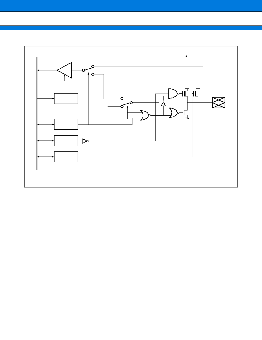
MB91133/MB91F133
44
∑ Block Diagram of Input / Output Port (Open-drain Output Function with Pull-up Resistance)
∑ Pull-up resistance control register (PCR) R/W
Controls pull up resistance ON/OFF.
0 : Without pull-up resistance
1 : With pull-up resistance
∑ Open-drain control register (ODCR) R/W
Controls open-drain in output mode.
0 : Standard output port in output mode
1 : Open-drain output port in output mode
Notes :
∑
This has no meaning in input mode (output Hi-Z) . Input/output mode is decided by the Direction Register
(DDR) .
∑
Pull-up resistance control register setting is handled as the priority in stop mode (HIZ
=
1) as well.
∑
Use of both the pull-up resistance control function and open-drain control function are prohibited when the
pin concerned is used as an external bus pin. "1" should not be written in both registers.
Data bus
PDR read
0
1
0
1
pin
PDR
DDR
ODCR
PCR
PDR
DDR
ODCR
PCR
: Port Data Register
: Data Direction Register
: OpenDrain Control Register
: Pull-up Control Register
Resource input
Resource output
Resource output
permission
MB91133/MB91F133
45
∑ Port Data Register (PDR)
PDR2 to L are input/output data registers of the I/O port.
Input/output control is carried out by DDR2 to L that are handled.
PDR2
Initial value
Access
Address : 000001
H
XXXXXXXX
B
R/W
PDR3
Initial value
Access
Address : 000000
H
XXXXXXXX
B
R/W
PDR4
Initial value
Access
Address : 000007
H
XXXXXXXX
B
R/W
PDR5
Initial value
Access
Address : 000006
H
XXXXXXXX
B
R/W
PDR6
Initial value
Access
Address : 000005
H
XXXXXXXX
B
R/W
PDR8
Initial value
Access
Address : 00000B
H
- XXXXXXX
B
R/W
PDRC
Initial value
Access
Address : 000013
H
XXXXXXXX
B
R/W
PDRD
Initial value
Access
Address : 000012
H
XXXXXXXX
B
R/W
PDRE
Initial value
Access
Address : 000011
H
XXXXXXXX
B
R/W
PDRF
Initial value
Access
Address : 000010
H
XXXXXXXX
B
R/W
PDRG
Initial value
Access
Address : 000017
H
- - XXXXXX
B
R/W
PDRH
Initial value
Access
Address : 000016
H
- - - - - XXX
B
R/W
PDRI
Initial value
Access
Address : 000015
H
- - XXXXXX
B
R/W
PDRJ
Initial value
Access
Address : 000014
H
- - XXXXXX
B
R/W
PDRK
Initial value
Access
Address : 00001B
H
XXXXXXXX
B
R/W
PDRL
Initial value
Access
Address : 00001A
H
XXXXXXXX
B
R/W
7
6
5
4
3
2
1
0
P26
P27
P25
P24
P23
P22
P21
P20
7
6
5
4
3
2
1
0
P36
P37
P35
P34
P33
P32
P31
P30
7
6
5
4
3
2
1
0
P46
P47
P45
P44
P43
P42
P41
P40
7
6
5
4
3
2
1
0
P56
P57
P55
P54
P53
P52
P51
P50
7
6
5
4
3
2
1
0
P66
P67
P65
P64
P63
P62
P61
P60
7
6
5
4
3
2
1
0
P86
P85
P84
P83
P82
P81
P80
7
6
5
4
3
2
1
0
PC6
PC7
PC5
PC4
PC3
PC2
PC1
PC0
7
6
5
4
3
2
1
0
PD6
PD7
PD5
PD4
PD3
PD2
PD1
PD0
7
6
5
4
3
2
1
0
PE6
PE7
PE5
PE4
PE3
PE2
PE1
PE0
7
6
5
4
3
2
1
0
PF6
PF7
PF5
PF4
PF3
PF2
PF1
PF0
7
6
5
4
3
2
1
0
PG5
PG4
PG3
PG2
PG1
PG0
7
6
5
4
3
2
1
0
PH2
PH1
PH0
7
6
5
4
3
2
1
0
PI5
PI4
PI3
PI2
PI1
PI0
7
6
5
4
3
2
1
0
PJ5
PJ4
PJ3
PJ2
PJ1
PJ0
7
6
5
4
3
2
1
0
PK6
PK7
PK5
PK4
PK3
PK2
PK1
PK0
7
6
5
4
3
2
1
0
PL6
PL7
PL5
PL4
PL3
PL2
PL1
PL0
MB91133/MB91F133
46
∑ Data Direction Register (DDR)
DDR0 to L control input/output direction of the I/O ports handled per bit.
DDR
=
0 : Port input
DDR
=
1 : Port output
"0" must be written into the empty bit.
DDR2
Initial value Access
Address : 000601
H
00000000
B
W
DDR3
Initial value Access
Address : 000600
H
00000000
B
W
DDR4
Initial value Access
Address : 000607
H
00000000
B
W
DDR5
Initial value Access
Address : 000606
H
00000000
B
W
DDR6
Initial value Access
Address : 000605
H
00000000
B
W
DDR8
Initial value Access
Address : 00060B
H
- 0000000
B
W
DDRC
Initial value Access
Address : 0000D3
H
00000000
B
R/W
DDRD
Initial value Access
Address : 0000D2
H
00000000
B
R/W
DDRE
Initial value Access
Address : 0000D1
H
00000000
B
R/W
DDRF
Initial value Access
Address : 0000D0
H
00000000
B
R/W
DDRG
Initial value Access
Address : 0000D7
H
- - 000000
B
R/W
DDRH
Initial value Access
Address : 0000D6
H
- - - - - 000
B
R/W
DDRI
Initial value Access
Address : 0000D5
H
- - 000000
B
R/W
DDRJ
Initial value Access
Address : 0000D4
H
- - 000000
B
R/W
DDRK
Initial value Access
Address : 0000DB
H
00000000
B
R/W
DDRL
Initial value Access
Address : 0000DA
H
00000000
B
R/W
7
6
5
4
3
2
1
0
P26
P27
P25
P24
P23
P22
P21
P20
7
6
5
4
3
2
1
0
P36
P37
P35
P34
P33
P32
P31
P30
7
6
5
4
3
2
1
0
P46
P47
P45
P44
P43
P42
P41
P40
7
6
5
4
3
2
1
0
P56
P57
P55
P54
P53
P52
P51
P50
7
6
5
4
3
2
1
0
P66
P67
P65
P64
P63
P62
P61
P60
7
6
5
4
3
2
1
0
P86
P85
P84
P83
P82
P81
P80
7
6
5
4
3
2
1
0
PC6
PC7
PC5
PC4
PC3
PC2
PC1
PC0
7
6
5
4
3
2
1
0
PD6
PD7
PD5
PD4
PD3
PD2
PD1
PD0
7
6
5
4
3
2
1
0
PE6
PE7
PE5
PE4
PE3
PE2
PE1
PE0
7
6
5
4
3
2
1
0
PF6
PF7
PF5
PF4
PF3
PF2
PF1
PF0
7
6
5
4
3
2
1
0
PG5
PG4
PG3
PG2
PG1
PG0
7
6
5
4
3
2
1
0
PH2
PH1
PH0
7
6
5
4
3
2
1
0
PI5
PI4
PI3
PI2
PI1
PI0
7
6
5
4
3
2
1
0
PJ5
PJ4
PJ3
PJ2
PJ1
PJ0
7
6
5
4
3
2
1
0
PK6
PK7
PK5
PK4
PK3
PK2
PK1
PK0
7
6
5
4
3
2
1
0
PL6
PL7
PL5
PL4
PL3
PL2
PL1
PL0
MB91133/MB91F133
47
∑ Pull up Control Register (PCR)
∑ Open-drain Control Register (ODCR)
PCR6 to J carry out pull-up resistance control of the I/O ports handled.
PCR
=
0 : Pull-up resistance turned off
PCR
=
1 : Pull-up resistance turned on
PCR6
Initial value Access
Address : 000631
H
00000000
B
R/W
PCRC
Initial value Access
Address : 0000C3
H
00000000
B
R/W
PCRD
Initial value Access
Address : 0000C2
H
00000000
B
R/W
PCRE
Initial value Access
Address : 0000C1
H
- - - - - - 00
B
R/W
PCRH
Initial value Access
Address : 0000C6
H
- - - - - 000
B
R/W
PCRI
Initial value Access
Address : 0000C5
H
- - 000000
B
R/W
PCRJ
Initial value Access
Address : 0000C4
H
- - 000000
B
R/W
7
6
5
4
3
2
1
0
P66
P67
P65
P64
P63
P62
P61
P60
7
6
5
4
3
2
1
0
PC6
PC7
PC5
PC4
PC3
PC2
PC1
PC0
7
6
5
4
3
2
1
0
PD6
PD7
PD5
PD4
PD3
PD2
PD1
PD0
7
6
5
4
3
2
1
0
PE1
PE0
7
6
5
4
3
2
1
0
PH2
PH1
PH0
7
6
5
4
3
2
1
0
PI5
PI4
PI3
PI2
PI1
PI0
7
6
5
4
3
2
1
0
PJ5
PJ4
PJ3
PJ2
PJ1
PJ0
OCRH to J carry out open-drain control in output mode of the I/O ports handled.
OCR
=
0 : Standard output port in output mode
OCR
=
1 : Open-drain output port in output mode
This has no meaning in input mode (output Hi-z) .
OCRH
Initial value Access
Address : 0000CA
H
- - - - - 000
B
R/W
OCRI
Initial value Access
Address : 0000C9
H
- - 000000
B
R/W
OCRJ
Initial value Access
Address : 0000C8
H
- - 000000
B
R/W
7
6
5
4
3
2
1
0
PH2
PH1
PH0
7
6
5
4
3
2
1
0
PI5
PI4
PI3
PI2
PI1
PI0
7
6
5
4
3
2
1
0
PJ5
PJ4
PJ3
PJ2
PJ1
PJ0
MB91133/MB91F133
48
∑ Analog Input Control Register (AICR)
AICK controls each pin of the I/O ports handled as follows.
AIC
=
0 : Analog input mode
AIC
=
1 : Port input mode
Set to "0" when reset.
AICK
Initial value Access
Address : 0000CF
H
00000000
B
R/W
7
6
5
4
3
2
1
0
PK6
PK7
PK5
PK4
PK3
PK2
PK1
PK0

MB91133/MB91F133
49
3.
8/16-bit Up/Down Counter / Timer
8/16-bit up/down counter / timer is configured of event input pins
◊
6, 8-bit up/down counters
◊
2, 8-bit reload /
compare registers
◊
2 and their control circuits.
∑ Characteristics of 8/16-bit Up/Down Counter / Timer
∑ Counting from (0) d to (256) d is possible using an 8-bit counting register.
(Counting from (0) d to (65535) d is possible in 16-bit
◊
1 operation mode.)
∑ 4 types of counting mode can be selected by the count clock
∑ Selection can be made from two types of internal clock as the count clock in timer mode.
∑ Detection edge of the external pin input signals can be selected in up/down count mode.
∑ Phase difference count mode is suited to count encoders such as motors. Turning angle and turning number,
etc., can easily and accurately be counted by separately inputting phase A, B and Z outputs of the encoder.
∑ Selection can be made from two function types for the ZIN pin (valid for all modes) .
∑ Compare and reload functions are featured, and each function can be used alone or in combination.
Up/down counting with random width can be carried out using both functions in combination.
∑ The count direction directly before can be identified by the count direction flag.
∑ Generation of interruptions in case of compared match, reload (underflow) or overflow and in cases where the
count direction is changed can be controlled separately.
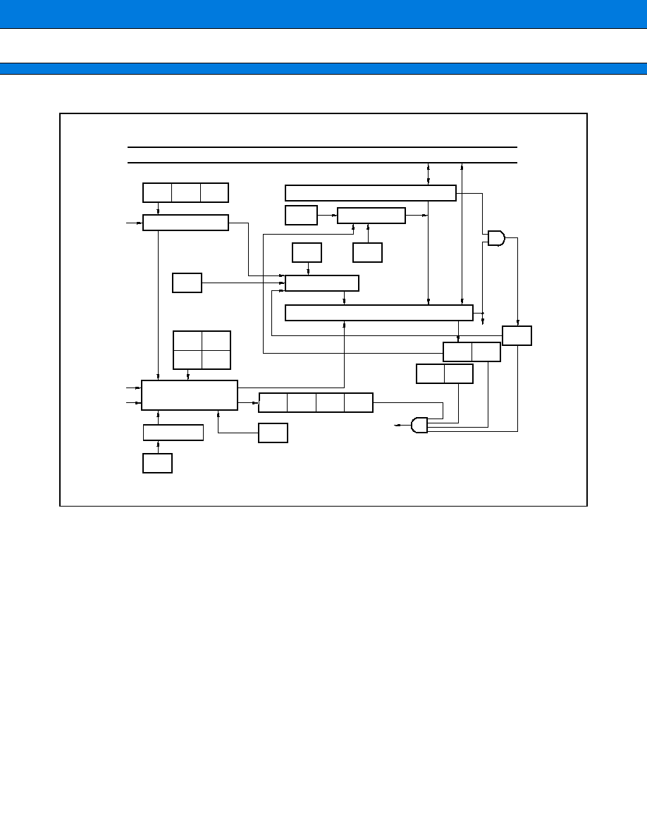
MB91133/MB91F133
50
∑ Block Diagram
CGE1 CGE0
Edge/level detection
C/GS
Carry
CMS1 CMS0
CES1 CES0
CITE
UDIE
UDF1 UDF0 CDCF CFIE
Count clock
Interruption output
RCUT
Reload control
Counter clear
Up/down count
clock selection
UCRE
8 bit
8 bit
Data bus
Reload / Compare Register 0 (RCR0)
Up/Down Count Register 0 (UDCR0)
RLDE
UDCC
CMPF
UDFF OVFF
CLKS
CSTR
Pre-scalar
AIN0
BIN0
ZIN0
8/16-bit Up/Down Counter / Timer (ch0)
MB91133/MB91F133
51
CGE1 CGE0 C/GS
Carry
Count clock
Interruption output
CITE
UDIE
UDF1
Up/down count
clock selection
UDF0 CDCF CFIE
RCUT
Reload control
Counter clear
Edge/level detection
UCRE
RLDE
UDCC
CMPF
UDFF OVFF
CLKS
CSTR
Pre-scalar
AIN1
BIN1
ZIN1
CMS1 CMS0 CES1 CES0 M16E
8 bit
8 bit
Data bus
Reload / Compare Register 1 (RCR1)
Up/Down Count Register 1 (UDCR1)
8/16-bit Up/Down Counter / Timer (ch1)
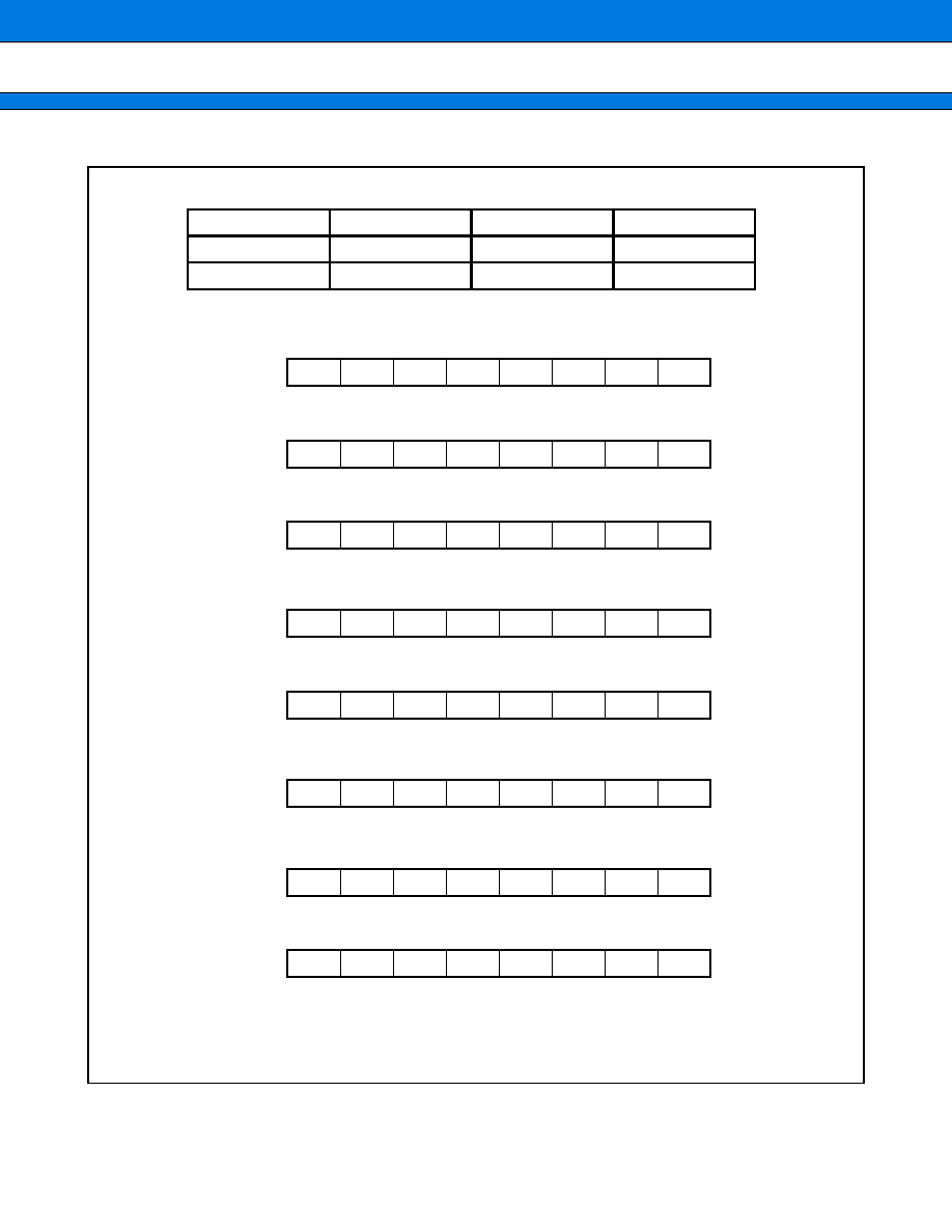
MB91133/MB91F133
52
∑ Register List
Up/down count register ch0 (UDCR0)
Up/down count register ch1 (UDCR1)
Reload compare register ch0 (RCR0)
Reload compare register ch1 (RCR1)
Counter Status register ch0, 1 (CSR0, 1)
Counter control register ch0, 1 (CCRL0, 1)
Counter control register ch0 (CCRH0)
Counter control register ch1 (CCRH1)
bit
Address : 000087
H
bit
Address : 000086
H
bit
Address : 000085
H
bit
Address : 000084
H
bit
Address :
00008B
H
00008F
H
bit
Address :
000089
H
00008D
H
bit
Address : 000088
H
bit
Address :00008C
H
15
8
UDCR1
7
0
31
24
RCR1
UDCR0
RCR0
CCRH0
CSR0
CCRL0
CCRH1
CSR1
CCRL1
23
16
7
6
5
4
3
2
1
0
D06
D07
D05
D04
D03
D02
D01
D00
15
14
13
12
11
10
9
8
D16
D17
D15
D14
D13
D12
D11
D10
7
6
5
4
3
2
1
0
D06
D07
D05
D04
D03
D02
D01
D00
15
14
13
12
11
10
9
8
D16
D17
D15
D14
D13
D12
D11
D10
7
6
5
4
3
2
1
0
CITE
CSTR
UDIE
CMPF
OVFF
UDFF
UDF1
UDF0
7
6
5
4
3
2
1
0
CTUT
UCRE
RLDE
UDCC
CGSC
CGE1
CGE0
15
14
13
12
11
10
9
8
CDCF
M16E
CFIE
CLKS
CMS1
CMS0
CES1
CES0
15
14
13
12
11
10
9
8
CDCF
CFIE
CLKS
CMS1
CMS0
CES1
CES0
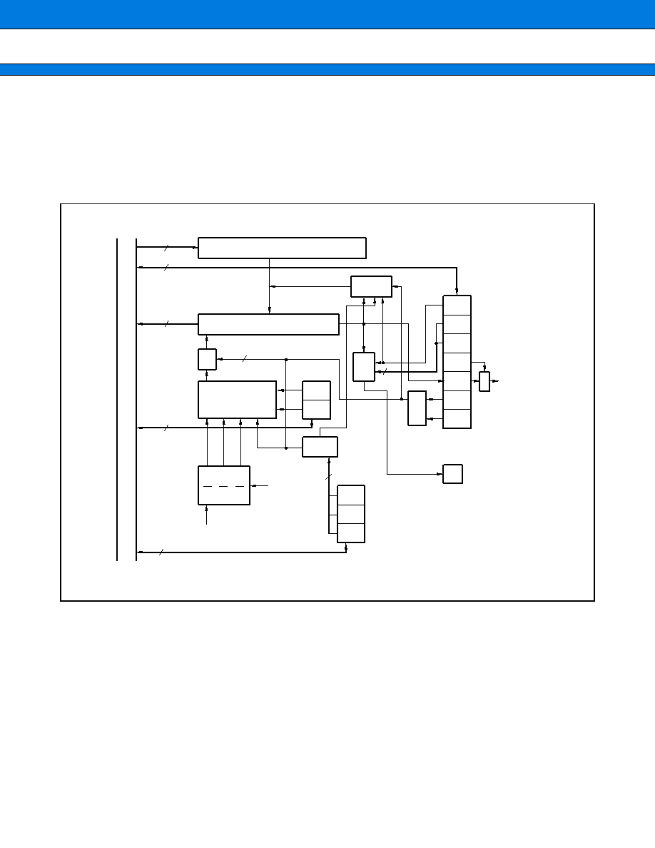
MB91133/MB91F133
53
4.
16-bit Reload Timer
The 16-bit timer is configured with a 16-bit down counter, 16-bit reload register, pre-scalar to prepare the internal
count clock and control register. Selection can be made from three types of internal clocks (machine clock 2 /
8 / 32 cycles) as the input clock. DMA transfer can be initiated by interruption. The MB91133/MB91F133 features
a 5-channel timer.
∑ Block Diagram
Channel 2TO output of the reload timer is connected to the A/D converter inside the LSI. Thus, A/D conversion
can be started up at the cycle set in the reload register.
RELD
OUTE
OUTL
INTE
UF
CNTE
TRG
OUT
CTL.
CSL1
CSL0
MOD2
MOD1
MOD0
16
8
16
2
R - BUS
3
2
UF
Reload
Clock selector
16-bit reload register
16-bit down counter
IN CTL.
2
2
2
1
3
5
3
EXCK
Pre-scalar
clear
GATE
2
Re-trigger
IRQ
PWM (ch0, ch1)
A/D (ch2)

MB91133/MB91F133
54
5.
PPG Timer
The PPG timer can efficiently output accurate PWM waveforms. The MB91130 series features a 6-channel
PPG timer.
∑ PPG Timer Characteristics
∑ Each channel is configured with a 16-bit down counter, 16-bit data register with cycle setting buffer, 16-bit
compare register with duty setting buffer and pin control area.
∑ Selection can be made from four types of count clocks for 16-bit down counters.
Internal clock
,
4,
16,
64
∑ Counter values can be initialized to "FFFF
H
" by resetting and counter borrowing.
∑ PWM output is available per channel.
∑ Register outline
Cycle setting register : Reloading register with buffer
Duty setting register : Compare register with buffer
Transfer from buffer is carried out by counter borrowing.
∑ Pin control outline
Set to "1" by duty match. (Priority)
Resets to "0" by counter borrowing.
All "L" (or "H") can simply be output by using the output values fixing mode.
Polarization can also be specified.
∑ Interruption request can be generated by selecting from the following combinations.
Initiation of this timer
Counter borrow generation (cycle match)
Duty match generation
Counter borrow generation (cycle match) or duty match generation
DMA transfer can be initiated by the above interruption requests.
∑ Simultaneous initiation of a number of channels can be set by software or other interval timers. Re-start during
operation can also be set.
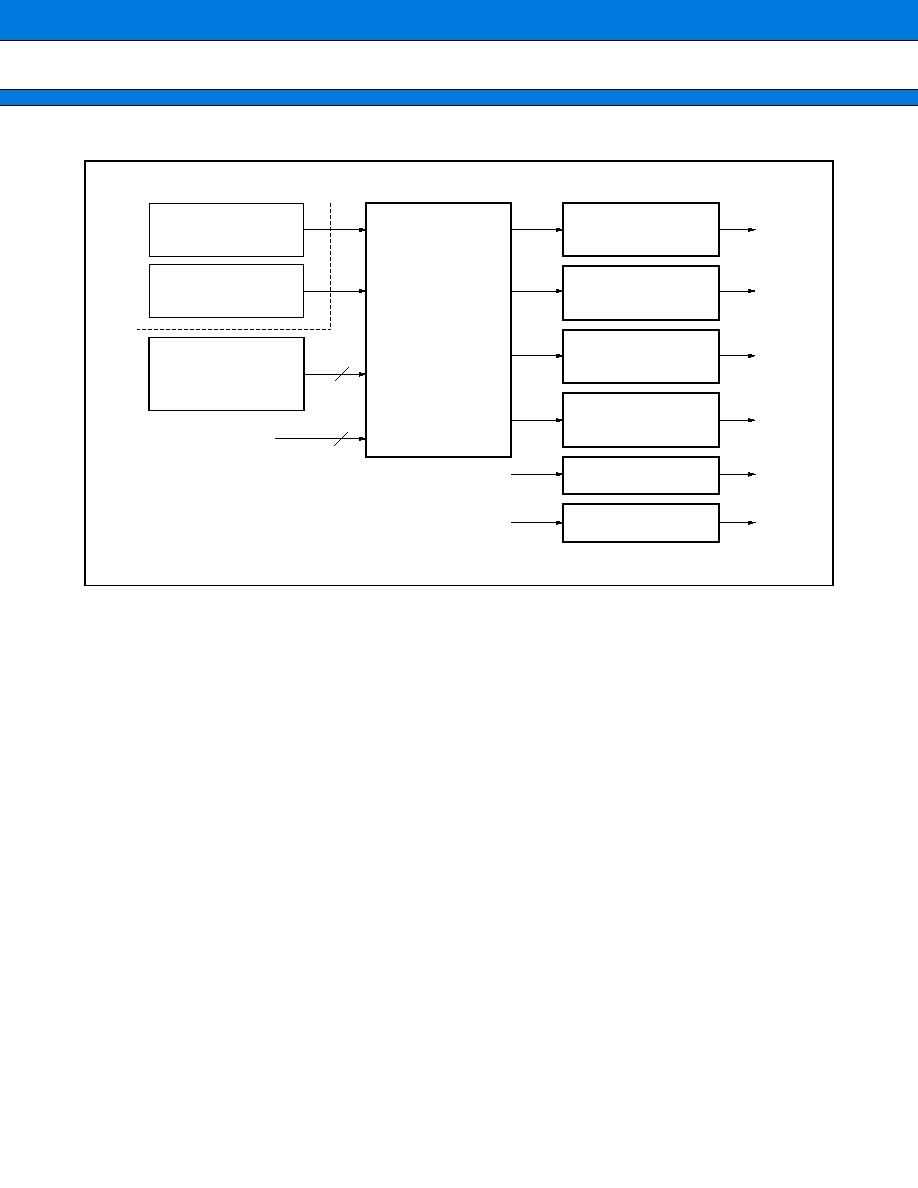
MB91133/MB91F133
55
∑ Block Diagram
4
4
PWM0
16-bit reload timer
ch0
General control
register 1
(factor selection)
16-bit reload timer
ch1
General control
register 2
External TRG0 to 3
External TRG4
External TRG5
TRG input
PWM timer ch0
TRG input
PWM timer ch1
TRG input
PWM timer ch2
TRG input
PWM timer ch3
PWM1
PWM2
PWM3
PWM4
PWM5
PWM timer ch4
PWM timer ch5
Overall Block Diagram of PPG Time
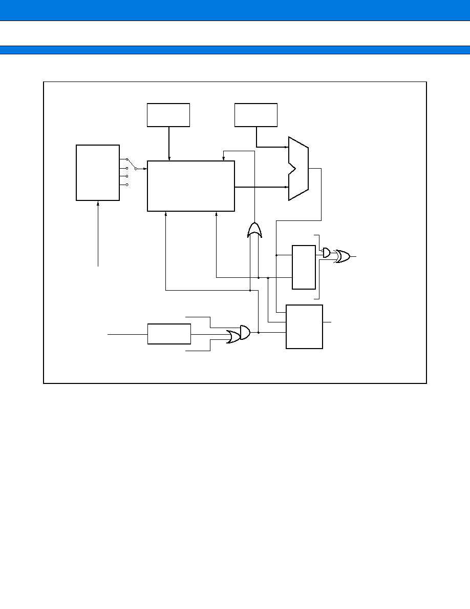
MB91133/MB91F133
56
1 / 1
1 / 4
1 / 16
1 / 64
CK
PWM OUTPUT
PCSR
PPG mask
Enable
TRG input
Soft trigger
Reverse bit
Load
PDUT
CMP
Interruption
selection
Edge
detection
Start
Borrow
Pre-scalar
16-bit down counter
Peripheral system clock
S
R
Q
IRQ
Block Diagram of PPG Timer for 1 Channel
MB91133/MB91F133
57
∑ Register list
(Continued)
GCN1
GCN2
PTMR
PCSR
PDUT
PCNH
PCNL
PTMR
PCSR
PDUT
PCNH
PCNL
PTMR
PCSR
PDUT
PCNH
R/W
R/W
R
W
W
R/W
R
W
W
R/W
R
W
W
R/W
15
Address
0
000000DF
H
000000E6
H
000000EE
H
000000F6
H
PCNL
PTMR
PCSR
PDUT
PCNH
PCNL
R
W
W
R/W
General control register 1
General control register 2
ch0 Timer register
ch0 Peripheral setting register
ch0 Duty setting register
ch0 Control status register
ch1 Timer register
ch1 Peripheral setting register
ch1 Duty setting register
ch1 Control status register
ch2 Timer register
ch2 Peripheral setting register
ch2 Duty setting register
ch2 Control status register
ch3 Timer register
ch3 Peripheral setting register
ch3 Duty setting register
ch3 Control status register
000000FE
H
000000DC
H
000000E4
H
000000EC
H
000000F4
H
000000FC
H
000000E2
H
000000EA
H
000000F2
H
000000FA
H
000000E0
H
000000E8
H
000000F0
H
000000F8
H
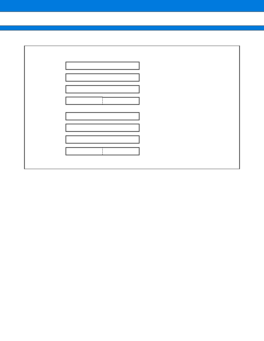
MB91133/MB91F133
58
(Continued)
15
0
PTMR
PCSR
PDUT
PCNH
R
W
W
R/W
00000106
H
PCNL
PTMR
PCSR
PDUT
PCNH
PCNL
R
W
W
R/W
ch4 Peripheral setting register
ch4 Duty setting register
ch4 Control status register
ch5 Timer register
ch5 Peripheral setting register
ch5 Duty setting register
ch5 Control status register
0000010E
H
00000104
H
0000010C
H
00000102
H
0000010A
H
00000100
H
00000108
H
Address
ch4 Timer register

MB91133/MB91F133
59
6.
Multifunction Timer
The multifunction timer unit is configured of a 16-bit freerun timer
◊
1, 16-bit output compare
◊
8, 16-bit input
capture
◊
4, 16-bit PPG timer
◊
6 ch and waveform generation area modules. 12 independent waveform outputs
based on a 16-bit free-run timer are possible using this function and measurement of input pulse width and
external clock cycle is also possible.
∑ Multifunction Timer Configuration
∑ 16-bit free-run timer (
◊
1)
The 16-bit free-run timer consists of a 16-bit up counter, control register, 16-bit compare clear register and
pre-scalar. Output values of this counter are used as the base timer for output compare and input capture.
∑
Counter operation clocks can be selected from six types.
Six types of internal clocks (
2,
4,
8,
16,
32,
64)
: Machine clock
∑
Interruption can be generated by overflow of the counter value and a compared match with compare
clear register. (Mode setting is required for a compared match.)
∑
Counter value can be initialized to "0000
H
" by a compared match with the reset, software clear or the
compare clear register.
∑ Output compare (
◊
8)
Output compare is configured of 16-bit compare register
◊
8, latch for compare output and control register.
Interruption can be generated as well as reversing output level when the 16-bit free-run timer value and compare
register value match.
∑
8 compare registers can be operated independently. Output pins and interruption flags support each
compare register.
∑
Output pins can be controlled by pairing two compare registers. Output pins are reversed using two
compare registers.
∑
Initial value of each output pin can be set.
∑
Interruption can be generated by matching compare.
∑ Input capture (
◊
4)
Input capture is configured with four independent external input pins , supported capture and control register.
16-bit free-run timer value is held in the capture register by detecting the random edge of signals that are input
by the external input pin, and interruption can simultaneously be generated.
∑
Valid edges (rising edge, falling edge, both edges) of external input signals can be selected.
∑
Four input captures can be operated independently.
∑
Interruption can be generated by the valid edges of external input signals.
∑ 16-bit PPG timer (
◊
6)
Refer to PPG timer

MB91133/MB91F133
60
∑ Waveform Generation Area
The waveform generation area is configured with 8-bit timer
◊
3, 8-bit reload register
◊
3, timer control register
◊
3 and 8-bit waveform control register. This control circuit controls the waveform of the 16-bit PPG timer and
real-time output, and DC chopper output and non-overlapping 3-phase waveform output to be used for inverter
control are possible.
∑
Non-overlapping pulse output of the PPG timer is possible by setting dead time of the 8-bit timer (dead
time timer function) .
∑
Real timer output is operated by the 2-channel mode and non-overlapping output of the waveform is
possible by setting the dead time of the 8-bit timer (dead time timer function) .
∑
Operation of PPG timer can easily be started/stopped by generating a GATE signal for the PPG timer
operation through match detection of real-time output compare (GATE function).
∑
The 8-bit timer is operated by match detection of real-time output compare, and operation of the PPG timer
can easily be started/stopped by generating a GATE signal for the PPG timer until the 8-bit timer is stopped
(GATE function) .
∑
Pin output can be forcibly controlled by input to the DTTI pin. Pins can be controlled externally even if
oscillations stop due to lack of clocks for inputs to this pin. (Each pin level can be set by the program .)
If this function is used, the port should be set to output (DDR
=
1) and the output value should be
described in the PDR beforehand.
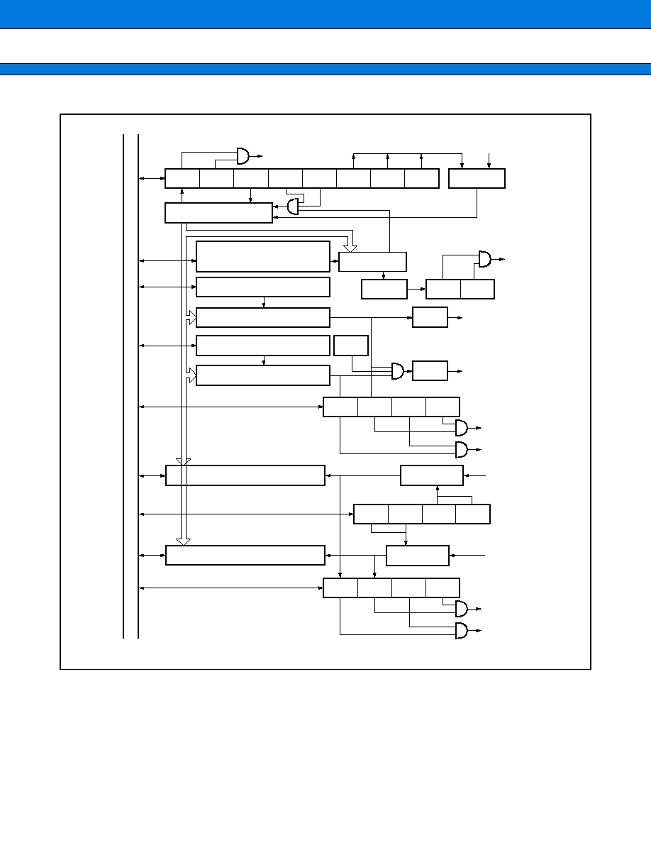
MB91133/MB91F133
61
∑ Block Diagram
IVF
R-BUS
IVFE
16-bit free-run timer
Compare register 0/2/4
Compare circuit
Compare register 1/3/5
Compare circuit
Capture data register 0/2
Capture data register 1/3
16-bit compare clear register
(Ch. 6 compare register)
STOP
MODE
SCLR
CLK2
CLK1
CLK0
Cycle device
ICLR
IOP1
IOP0
IOE1
IOE0
ICP0
ICP1
ICE0
ICE1
EG11
EG10
EG01
EG00
IN 0/2
IN 1/3
CMOD
RT0/2/4
Clock
Interruption
Interruption
Interruption
Interruption
Interruption
Interruption
T
Q
RT1/3/5
To waveform
generation area
To waveform
generation area
T
Q
ICRE
MS13
0
Compare circuit
Edge detection
Edge detection
Block Diagram of PPG Timer for 1 Channel
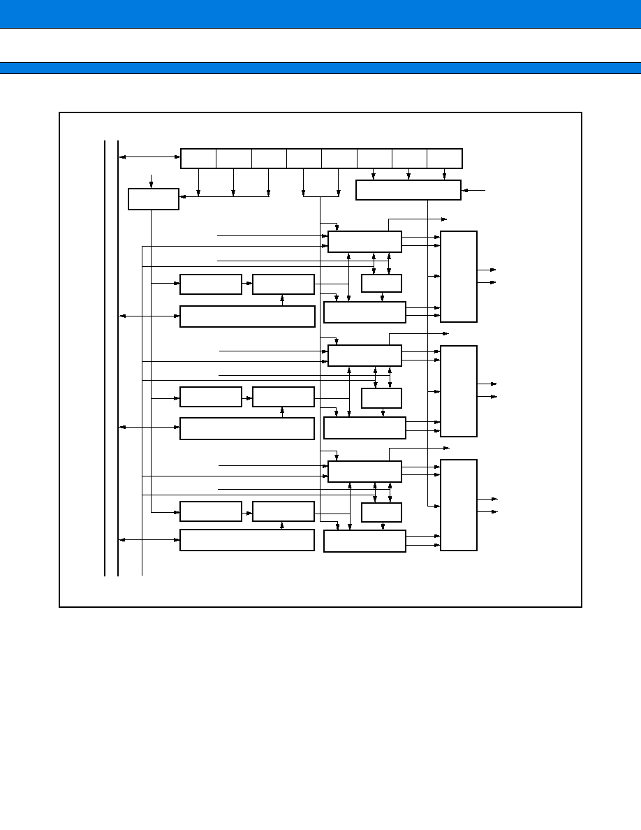
MB91133/MB91F133
62
R
-
BUS
DCK2
Cycle device
DTTI control circuit
Waveform
generation area
Dead time
generation
Clock
8-bit timer
8-bit timer register 0
Compare
circuit
Selector
Selector
Waveform
generation area
Dead time
generation
8-bit timer
8-bit timer register 1
Compare
circuit
Selector
Selector
Waveform
generation area
Dead time
generation
8-bit timer
8-bit timer register 2
Compare
circuit
Selector
Selector
DCK1
DCK0
TMD1
TMD0
NRSL
DTIL
DTIE
DTTI
GATE 0/1
TO0
TO1
RTO0/U
RTO1/X
RTO2/V
RTO3/Y
RTO4/W
RTO5/Z
U
X
TO2
TO3
V
Y
TO4
TO5
W
Z
GATE 2/3
GATE 4/5
RT4
RT5
RT2
RT3
RT0
RT1
Block Diagram of Waveform Generation Area
MB91133/MB91F133
63
∑ Registers List
15
Address
8 7
0
IPCP
OCCP
OCS
TCDT
TCCS
ICS
TMRR
STGCR
DTCR
(R)
(R/W)
(R/W)
(R/W)
(R/W)
(R/W)
(R/W)
(R/W)
(R/W)
000044
H
to 4B
H
00004D
H
, 4F
H
000054
H
to 63
H
000064
H
to 6B
H
00006C
H
, 6D
H
00006E
H
, 6F
H
0000AD
H
, AF
H
B3
H
0000B1
H
0000AC
H
, AE
H
B2
H
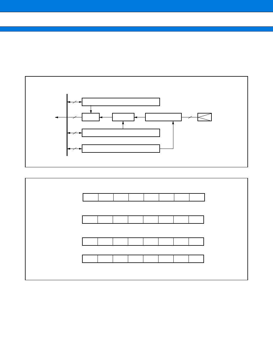
MB91133/MB91F133
64
7.
External Interruption
The external interruption control area is the block that controls the external interruption requests input in INT0
to INT23. The level of request to be detected can be selected from "H", "L", "Rising edge" or " Falling edge".
∑ Block diagram
∑ Register List
24
R-BUS
Interruption permission register
Gate
Interruption
requests
Factor F/F
Edge detection circuit
Interruption factor register
Request level setting register
24
48
24
24
INT0 to INT23
External interruption permission register (ENIR)
External interruption factor register (EIRR)
Request level setting register (ELVR)
There are three sets of the above registers (for 8 channels) for a total of 24 channels.
bit
bit
bit
bit
15
14
13
12
11
10
9
8
ER6
ER7
ER5
ER4
ER3
ER2
ER1
ER0
15
14
13
12
11
10
9
8
ER6
ER7
ER5
ER4
ER3
ER2
ER1
ER0
7
6
5
4
3
2
1
0
LA3
LB3
LB2
LA2
LB1
LA1
LB0
LA0
15
14
13
12
11
10
9
8
LA7
LB7
LB6
LA6
LB5
LA5
LB4
LA4

MB91133/MB91F133
65
8.
Delay Interruption Module
The delay interruption module generates interruptions for task switching. Interruption requests to the CPU can
be generated / cancelled using software with this module.
∑ Block Diagram
Refer to "9.(2) Block Diagram of Interruption Controller" for the block diagram of the delay interruption generation
area.
∑ Register List
Address : 00000430
H
DICR
bit 7
6
5
4
3
2
1
0
R/W
DLYI

MB91133/MB91F133
66
9.
Interruption Controller
The interruption controller carries out interruption reception and arbitration.
∑ Hardware configuration of the interruption controller
This module consists of the following items.
∑ ICR register
∑ Interruption priority judgement circuit
∑ Interruption level, interruption number (vector) generation area
∑ Cancellation request generation area for HOLD request
∑ Major interruption controller functions
This module has the following functions.
∑ Detection of interruption requests
∑ Priority grade judgement (depending on the level and number)
∑ Transferring interruption level of factors for the judgement results (to CPU)
∑ Transferring interruption number of factors for the judgement results (to CPU)
∑ Recovery instruction from stop mode by generating interruption
∑ Cancellation of HOLD request to the bus master
∑ Resetting Interruption Factors
There are restrictions between RETI instructions and those for resetting interruption factors in the interruption
routine.
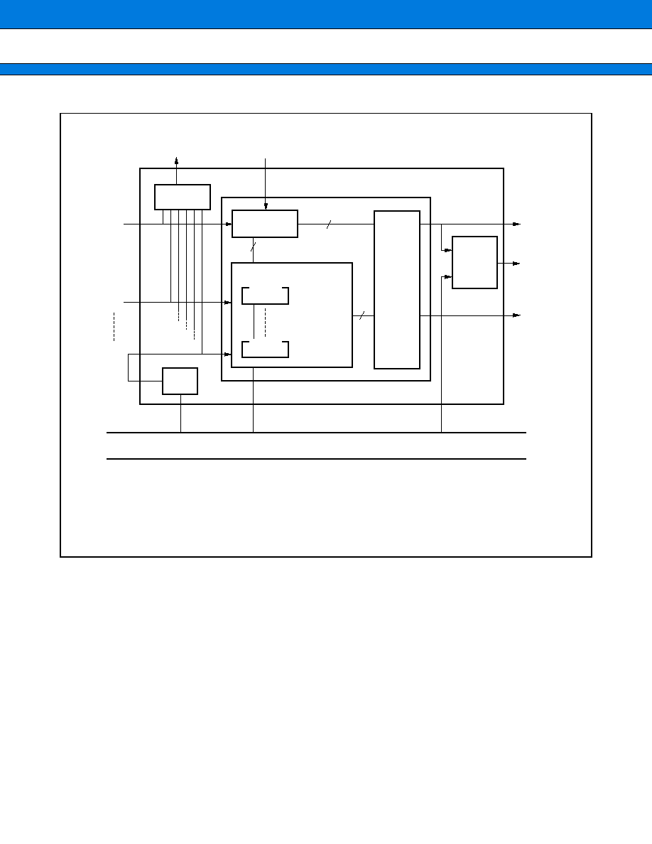
MB91133/MB91F133
67
∑ Block Diagram
IM
INT0
OR
NMI
RI00
RI47
(DLYIRQ)
DLYI
4
5
Priority grade judgement
6
HLDREQ
(Holding
request)
Generation
of
LEVEL /
VECTOR
VECTOR
judgement
LEVEL4 to 0
HLDCAN
VCT5 to 0
ICR00
LEVEL
judgement
NMI processing
ICR47
R-BUS
Note : DLYI shown in the figure indicates delay interruption area. (Refer to the chapter on the delay interruption
module for details.)
INTO is the wake-up signal to the clock control area in case of sleep or stop.
HLDCAN is the bus vacation request signal to bus masters other than the CPU.
There is no NMI function in this model.

MB91133/MB91F133
68
∑ Register List
(Continued)
Address :
Address :
Address :
Address :
Address :
Address :
Address :
Address :
Address :
Address :
Address :
Address :
Address :
Address :
Address :
Address :
Address :
Address :
Address :
Address :
Address :
Address :
Address :
Address :
Address :
Address :
Address :
Address :
Address :
Address :
Address :
Address :
bit 7
6
5
4
3
2
1
0
ICR3
ICR2
ICR1
ICR0
ICR3
ICR2
ICR1
ICR0
ICR3
ICR2
ICR1
ICR0
ICR3
ICR2
ICR1
ICR0
ICR3
ICR2
ICR1
ICR0
ICR3
ICR2
ICR1
ICR0
ICR3
ICR2
ICR1
ICR0
ICR3
ICR2
ICR1
ICR0
ICR3
ICR2
ICR1
ICR0
ICR3
ICR2
ICR1
ICR0
ICR3
ICR2
ICR1
ICR0
ICR3
ICR2
ICR1
ICR0
ICR3
ICR2
ICR1
ICR0
ICR3
ICR2
ICR1
ICR0
ICR3
ICR2
ICR1
ICR0
ICR3
ICR2
ICR1
ICR0
ICR3
ICR2
ICR1
ICR0
ICR3
ICR2
ICR1
ICR0
ICR3
ICR2
ICR1
ICR0
ICR3
ICR2
ICR1
ICR0
ICR3
ICR2
ICR1
ICR0
ICR3
ICR2
ICR1
ICR0
ICR3
ICR2
ICR1
ICR0
ICR3
ICR2
ICR1
ICR0
ICR3
ICR2
ICR1
ICR0
ICR3
ICR2
ICR1
ICR0
ICR3
ICR2
ICR1
ICR0
ICR3
ICR2
ICR1
ICR0
ICR3
ICR2
ICR1
ICR0
ICR3
ICR2
ICR1
ICR0
ICR3
ICR2
ICR1
ICR0
ICR3
ICR2
ICR1
ICR0
ICR00
ICR01
ICR02
ICR03
ICR04
ICR05
ICR06
ICR07
ICR08
ICR09
ICR10
ICR11
ICR12
ICR13
ICR14
ICR15
ICR16
ICR17
ICR18
ICR19
ICR20
ICR21
ICR22
ICR23
ICR24
ICR25
ICR26
ICR27
ICR28
ICR29
ICR30
ICR31
00000400
H
00000401
H
00000402
H
00000403
H
00000404
H
00000405
H
00000406
H
00000407
H
00000408
H
00000409
H
0000040A
H
0000040B
H
0000040C
H
0000040D
H
0000040E
H
0000040F
H
00000410
H
00000411
H
00000412
H
00000413
H
00000414
H
00000415
H
00000416
H
00000417
H
00000418
H
00000419
H
0000041A
H
0000041B
H
0000041C
H
0000041D
H
0000041E
H
0000041F
H
R/W
R/W
R/W
R/W
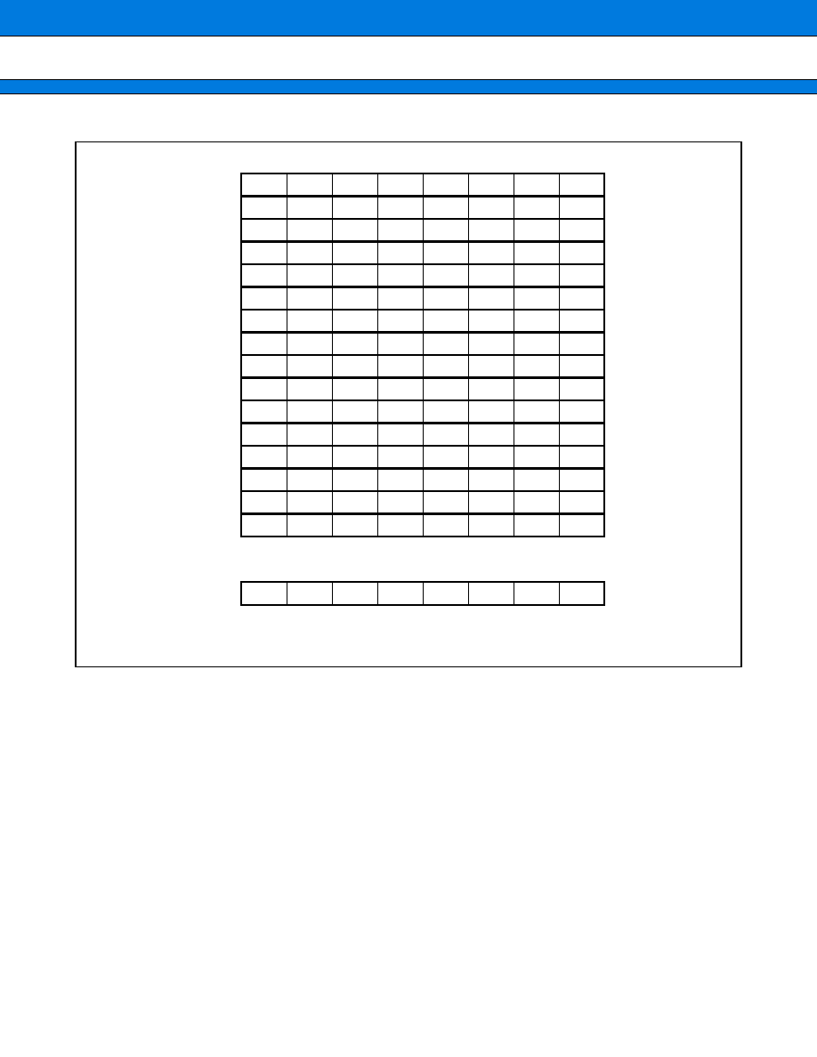
MB91133/MB91F133
69
(Continued)
Address :
Address :
Address :
Address :
Address :
Address :
Address :
Address :
Address :
Address :
Address :
Address :
Address :
Address :
Address :
Address :
Address :
bit 7
6
5
4
3
2
1
0
ICR3
ICR2
ICR1
ICR0
ICR3
ICR2
ICR1
ICR0
ICR3
ICR2
ICR1
ICR0
ICR3
ICR2
ICR1
ICR0
ICR3
ICR2
ICR1
ICR0
ICR3
ICR2
ICR1
ICR0
ICR3
ICR2
ICR1
ICR0
ICR3
ICR2
ICR1
ICR0
ICR3
ICR2
ICR1
ICR0
ICR3
ICR2
ICR1
ICR0
ICR3
ICR2
ICR1
ICR0
ICR3
ICR2
ICR1
ICR0
ICR3
ICR2
ICR1
ICR0
ICR3
ICR2
ICR1
ICR0
ICR3
ICR2
ICR1
ICR0
ICR3
ICR2
ICR1
ICR0
R/W
R/W
R/W
R/W
LVL3
LVL2
LVL1
LVL0
R/W
R/W
R/W
R/W
ICR32
ICR33
ICR34
ICR35
ICR36
ICR37
ICR38
ICR39
ICR40
ICR41
ICR42
ICR43
ICR44
ICR45
ICR46
ICR47
HRCL
00000420
H
00000421
H
00000422
H
00000423
H
00000424
H
00000425
H
00000426
H
00000427
H
00000428
H
00000429
H
0000042A
H
0000042B
H
0000042C
H
0000042D
H
0000042E
H
0000042F
H
00000431
H
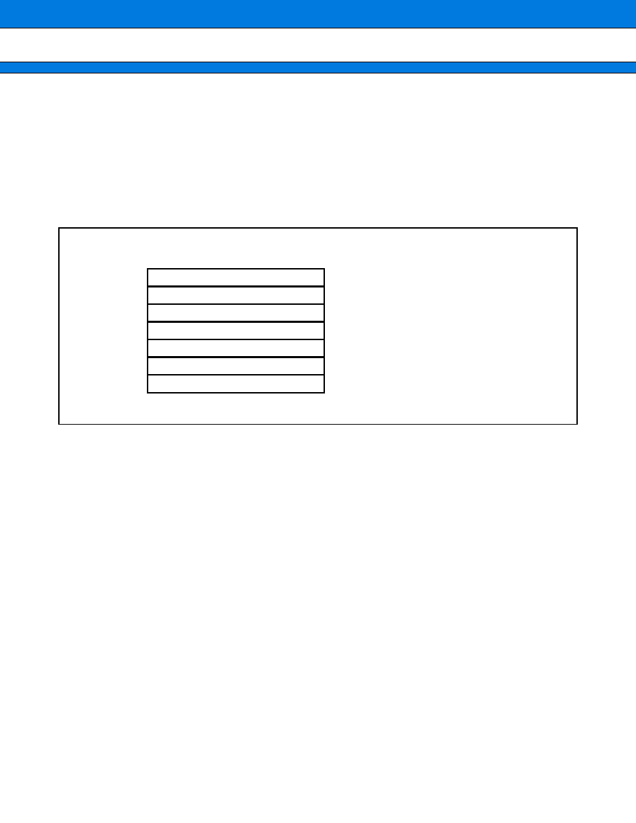
MB91133/MB91F133
70
10. Clock Generation Area (low power consumption mechanism)
Clock generation area is a module with the following functions.
∑ CPU clock generation (including gear function)
∑ Peripheral clock generation (including gear function)
∑ Reset generation and holding factors
∑ Standby function (including hardware standby)
∑ PLL (Phase Locked Loop) is built in
∑ Register list
7
Reset factor / watchdog cycle control register
Standby control register
DMA request blocking register
Time base timer clear register
Gear control register
Watchdog reset generation postponement register
PLL / 32-K clock control register
Address
RSRR/WTCR
STCR
PDRR
CTBR
000480
H
000481
H
000482
H
000483
H
GCR
WPR
PCTR
000484
H
000485
H
000488
H
0
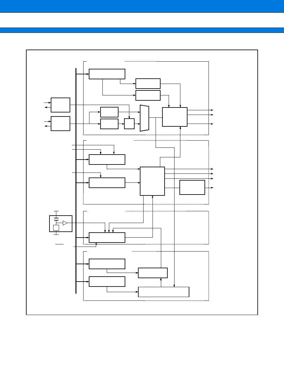
MB91133/MB91F133
71
∑ Block diagram
X0
Count clock
X1
X0A
CPU clock
Internal
bus clock
Internal
peripheral clock
STOP status
SLEEP status
CPU hold request
Internal reset
32-kHz selection circuit
[ Gear control area ]
[ Stop/sleep control area ]
[ Reset factor circuit ]
[ Watchdog control area ]
X1A
V
CC
3
GND
RST pin
M
P
X
PLL
STCR register
PDRR register
RSRR register
WPP register
Watchdog F/F
Time base timer
CTBR register
Internal interruption
Internal reset
DMA request
Power on
detection circuit
1
/
2
CPU gear
Peripheral
gear
Internal clock
generation
circuit
Status
transfer
control circuit
Reset
generation
F/F
GCR register
Oscillation
circuit
Oscillation
circuit
R
MB91133/MB91F133
72
11. 8-/10-bit A/D Converter
The 8-/10-bit A/D converter features functions that convert analog input voltages to 10- or 8-bit digital values
using the RC sequential comparison conversion method. The input signal is selected from 8-channel analog
input pins and three types of conversion initiation can be selected from software, internal clock, or external pin
trigger.
∑ characteristics of 8-/10-bit A/D converter
The A/D conversion function for converting analog voltages (input voltages) input into the analog input pins to
digital values has the following characteristics.
∑ Conversion time is minimum 5.0
µ
s (including sampling time when machine clock is 33 MHz) .
∑ Conversion method is RC sequential comparison conversion method with sample holding circuit.
∑ 10- or 8-bit resolution can be selected.
∑ Analog input pin can be selected from 8 channels using the program.
∑ interruption request can be generated when A/D conversion ends.
∑ Data is not lost even during continuous conversion as conversion data protection function works while inter-
ruptions are permitted.
∑ Initiation factors for conversion can be selected from software, 16-bit reload timer 2 (rising edge) , or external
pin trigger (L level detection) .
There are three types of conversion modes.
Table 13.1-1 Conversion Modes of 8-/10-bit A/D Converter
Conversion Modes
Single Conversion Operation
Scan Conversion Operation
Single conversion mode
Converts the specified channel (1 channel
only) once and ends.
Converts a series of channels (up to 8
channels can be specified) once and ends.
Consecutive
conversion mode
Repeatedly converts the specified channel
(1 channel only) .
Repeatedly converts a series of channels
(up to 8 channels can be specified) .
Stop conversion mode
Suspends after converting the specified
channel (1 channel only) once and waits
until the next one is initiated.
Converts a series of channels (up to 8
channels can be specified) but is suspend-
ed between each channel conversion and
waits until the next one is initiated.
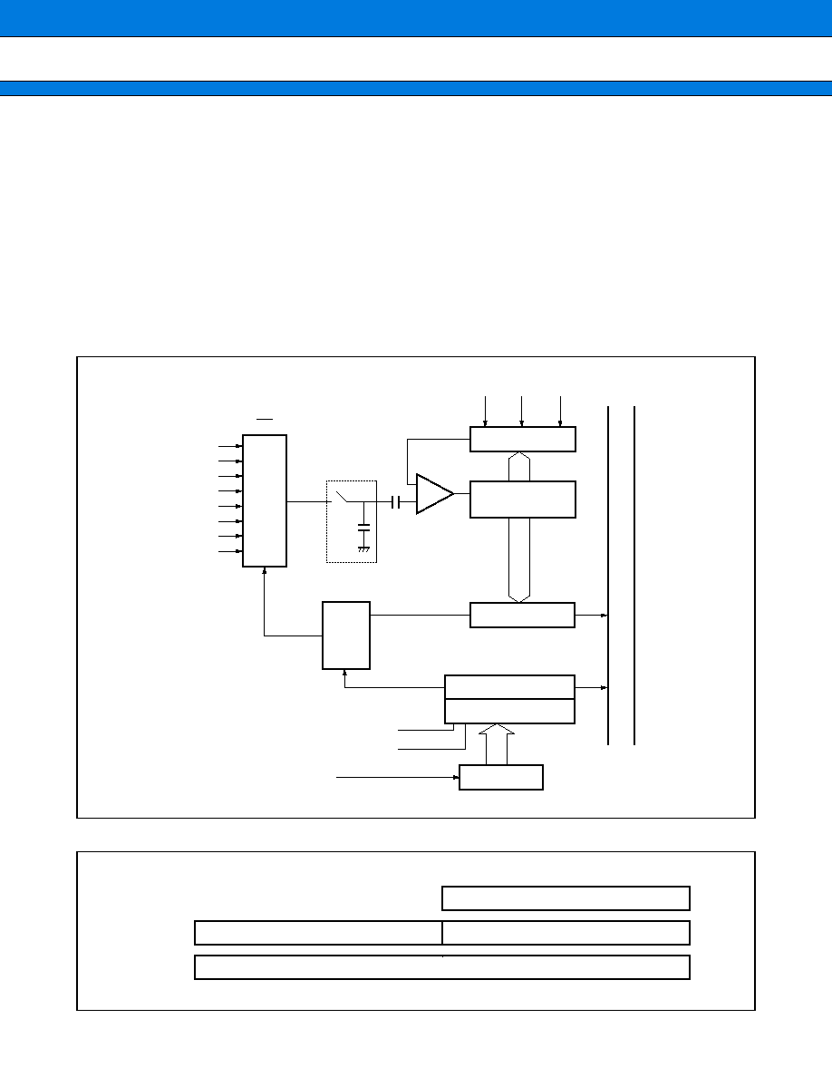
MB91133/MB91F133
73
∑ Block Diagram of 8-/10-bit A/D Converter
The 8-/10-bit A/D converter is configured with the following 9 blocks.
∑ A/D control status register (ADCS1, 2)
∑ A/D data register (ADCR)
∑ Clock selector (input clock selector to initiate A/D conversion)
∑ Decoder
∑ Analog channel selector
∑ Sample holding circuit
∑ D/A converter
∑ Comparator
∑ Control circuit
∑ Block Diagram
∑ Register List
MP
Comparator
Decoder
Input
circuit
AN0
AN1
AN2
AN3
AN4
AN5
AN6
AN7
Sample and
holding circuit
Operation clock
ADCR
ADCS1
,
2
Pre-scalar
16-bit reload timer 2
External pin trigger
AV
SS
D/A converter
Data register
A/D control register 1
A/D control register 2
Sequential
comparison register
AVR
±
AV
SS
R - BUS
15
14
13
12
11
10
9
8
7
6
5
4
3
2
1
0
0000CF
H
00003A
H
ADCS1
000038
H
AICK
ADCS0
ADCR
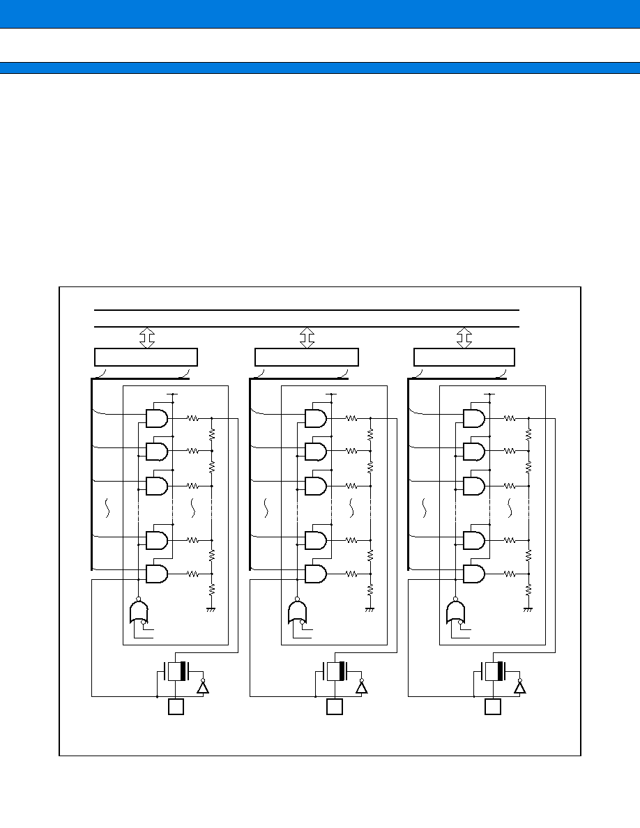
MB91133/MB91F133
74
12. 8-bit D/A Converter
The 8-bit D/A converter is an R-2R type D/A converter with 8-bit resolution.
∑ Characteristics of the 8-bit D/A converter
The MB81130 series features a 3-channel D/A converter and output control can be carried out individually by
the D/A control register.
∑ Block Diagram of 8-bit D/A Converter
The 8-bit D/A converter is configured with the following three blocks.
∑ 8-bit resistance ladder
∑ Data register
∑ Control register
∑ Block Diagram
DA27
DA27 to DA20
DA17 to DA10
DA07 to DA00
DAVC
DA20
DA output
DA output
DA output
DAE
DAE
DAE
Standby control
Standby control
Standby control
DA17
DAVC
DA10
DA07
DAVC
DA00
R
-
BUS
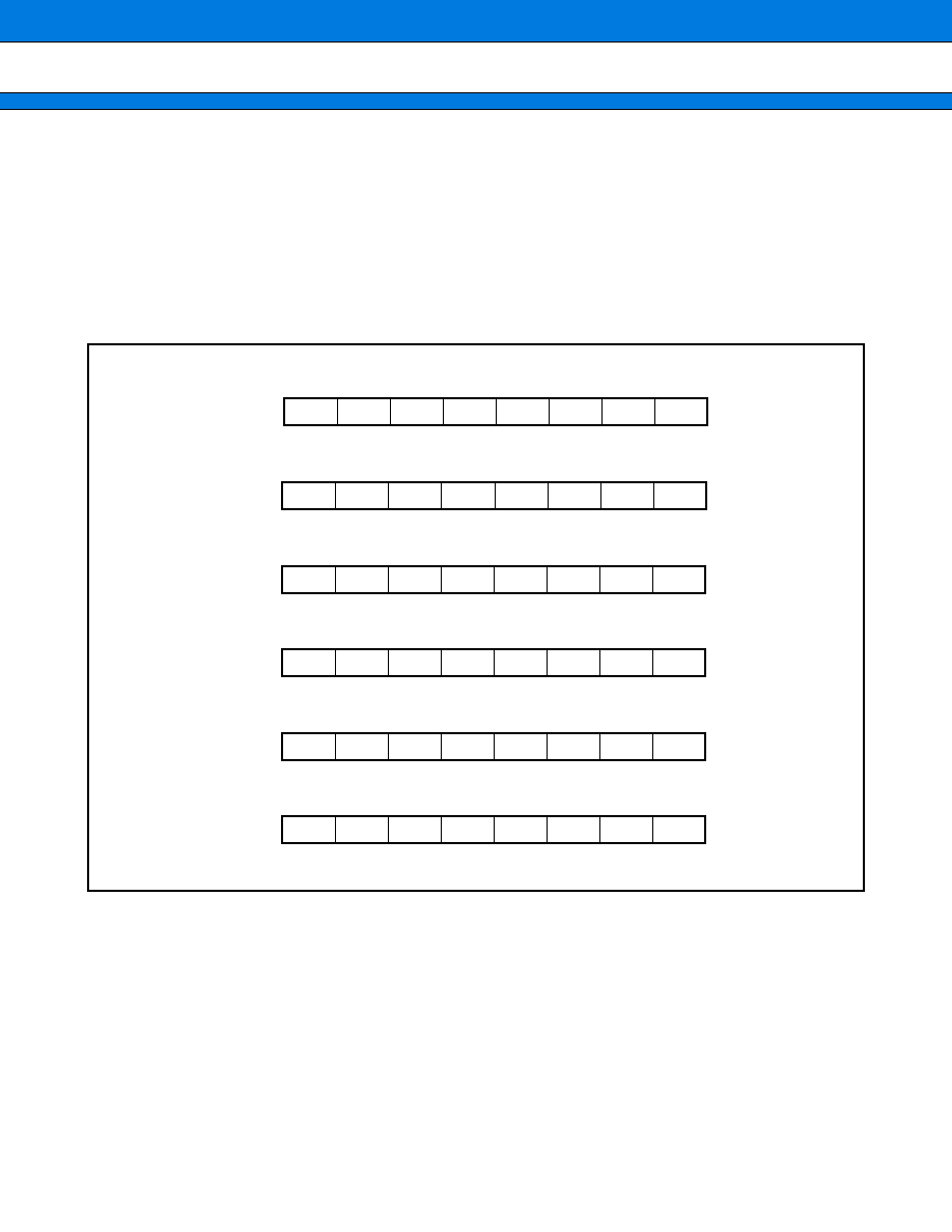
MB91133/MB91F133
75
∑ 8-bit D/A Converter Pins
D/A converter pins are dedicated pins.
∑ Registers of 8-bit D/A Converter
The 8-bit D/A converter has the following two registers.
D/A control register (DACR0, 1, 2)
D/A data register (DADR2, 1, 0)
∑ Register list
D/A converter data register 0
D/A converter data register 1
D/A converter data register 2
D/A control register 0
D/A control register 1
D/A control register 2
bit
DADR0
00000AB
H
bit
DADR1
00000AA
H
bit
DADR2
00000A9
H
bit
DACR0
00000A7
H
bit
DACR1
00000A6
H
bit
DACR2
00000A5
H
7
6
5
4
3
2
1
0
DA06
DA07
DA05
DA04
DA03
DA02
DA01
DA00
15
14
13
12
11
10
9
8
DA16
DA17
DA15
DA14
DA13
DA12
DA11
DA10
23
22
21
20
19
18
17
16
DA26
DA27
DA25
DA24
DA23
DA22
DA21
DA20
7
6
5
4
3
2
1
0
DAE0
15
14
13
12
11
10
9
8
DAE1
23
22
21
20
19
18
17
16
DAE2
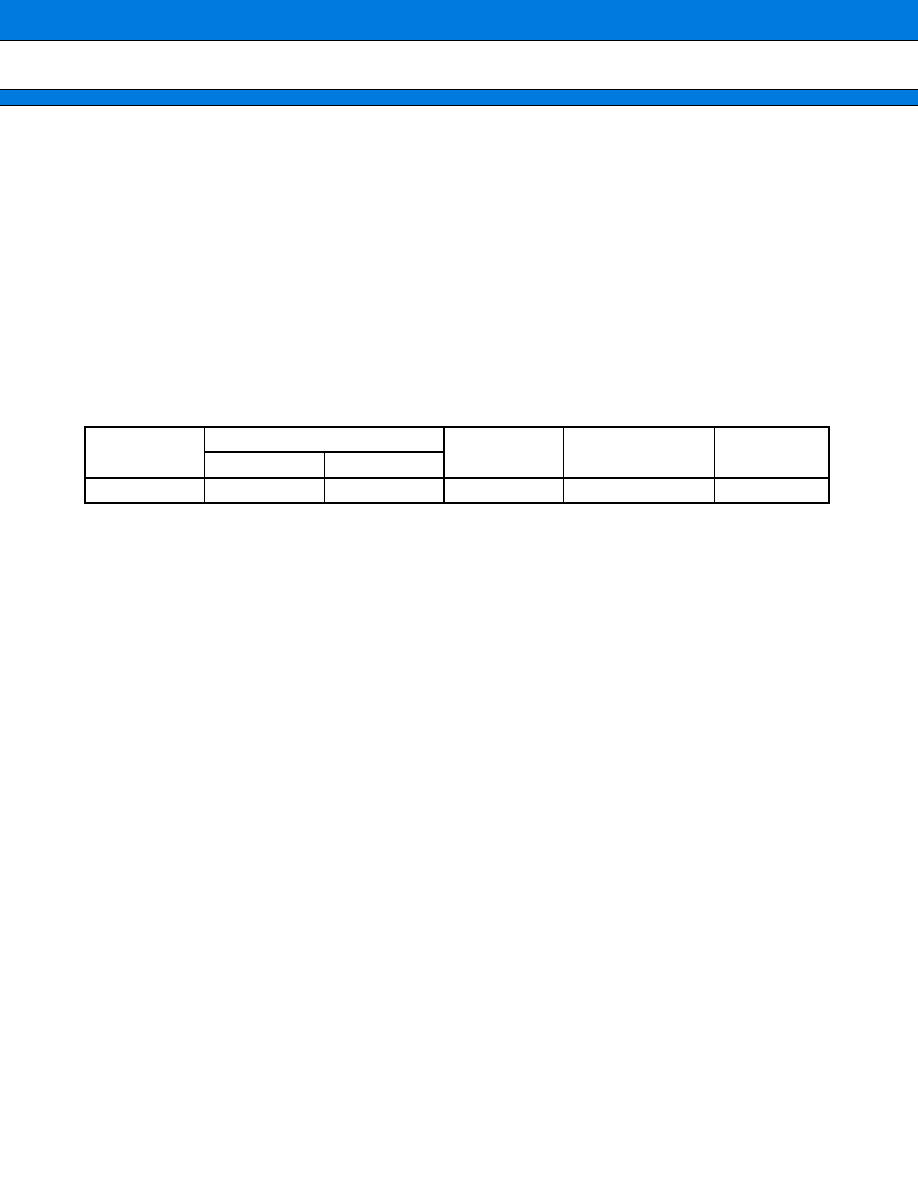
MB91133/MB91F133
76
13. 4-bit Level Comparator
The 4-bit level comparator is the module that compares input levels (large/small) and compares the size of the
analog input voltage with 4-bit digital values.
∑ Functions of the 4-bit level comparator
Compares analog voltage that has been input to the analog input pins (input voltage) with 4-bit digital value and
has the following characteristics.
∑ Conversion time is minimum 1
µ
s (including sampling time) .
∑ Sampling time is minimum 0.5
µ
s.
∑ Interruption requests can be generated when analog comparison ends.
∑ Interruption of 4-bit level comparator
Table 15.1-1 Interruption and DMAC of 4-bit level comparator
◊
: Initiation is impossible
Interruption
number
Interruption control register
Offset
TBR default
address
DMAC
Register name
Address
#61 (3D
H
) ICR45
00042D
H
308
H
000FFF08
H
◊
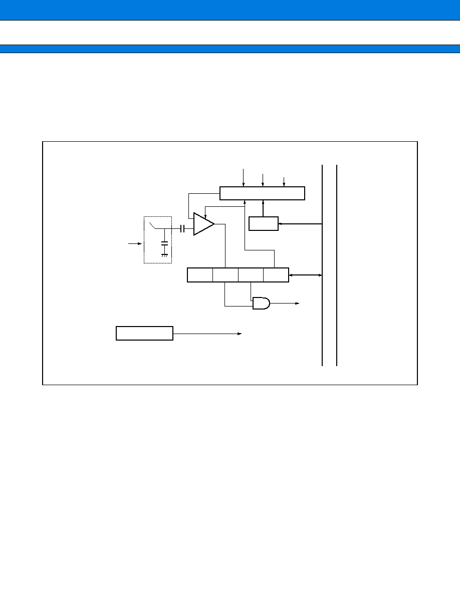
MB91133/MB91F133
77
∑ Block Diagram of 4-bit Level Comparator
The 4-bit level comparator is configured with the following three blocks.
∑ Comparator
∑ 4-bit resistance ladder
∑ Control register
∑ Block diagram
AN7
Interruption
Sample &
holding circuit
AV
CC
RD3 - 0
Comparator
Reload timer
Operation clock
AVR
±
4-bit D/A (resistance ladder)
AV
SS
FR30 R - BUS
CPLV
INT
INTE
CPEN
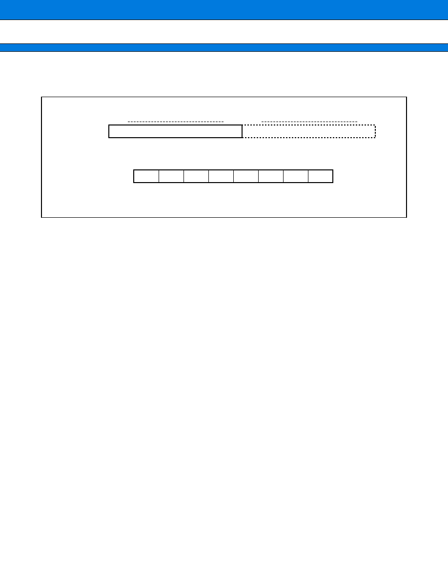
MB91133/MB91F133
78
∑ Registers of 4-bit Lev el Comparator
∑ Register list
Control register (LVLC)
bit
0000018
H
Attribute
Initial value
0000-0018
H
bit 31
bit 24
LVLC
bit 23
bit 16
R/W
( X )
R/W
( X )
R/W
( X )
R/W
( 0 )
R/W
( 0 )
R/W
( 0 )
R/W
( 0 )
31
30
29
28
27
26
25
24
RD2
R/W
( X )
RD3
RD1
RD0
CPLV
INT
INTE
CPEN
MB91133/MB91F133
79
14. UART
UART is the general-purpose serial data communications interface to carry out synchronous or asynchronous
communication (start-stop synchronization) with external systems. It has a master/slave-type communications
function (multiprocessor mode: supporting only master side) as well as normal bi-directional communications
function (normal mode).
∑ UART Functions
UART is the general-purpose serial data communications interface that sends and receives serial data to/from
other CPUs and peripheral equipment, and has functions shown in Table 16.1-1.
Table 16.1-1 UART Functions
Note : Start
/
stop bits are not added by UART and only data is transferred.
Table 16.1-2 UART Operations Mode
: Setting is impossible
*1 : "
+
1" is address
/
data selection bit (A/D) to be used to control communications.
*2 : 1-bit only can be detected for stop bit in case of reception.
Operations mode
Data length
Synchronization
method
Stop bit length
Without parity
With parity
0
Normal mode
7-bit or 8-bit
Asynchronous
1-bit or 2-bit
*2
1
Multiprocessor mode
8
+
1*
1
Asynchronous
2
Normal mode
8
Synchronous
N/A
Functions
Data buffer
Full-duplex double buffer
Transfer mode
∑ Clock synchronous (without start-stop bit)
∑ Clock asynchronous (start-stop cycle)
Baud rate
∑ Dedicated baud rate generator is available. Can be selected from 8 types.
∑ External clock input is possible.
∑ Internal clock (Internal clocks that are provided from 16-bit reload timer support-
ing each channel can be used.)
Data length
∑ 7-bit (in case of asynchronous normal mode only)
∑ 8-bit
Signal method
Non Return to Zero (NRZ) method
Reception error detection
∑ Framing error
∑ Overrun error
∑ Parity error (impossible in case of multiprocessor mode)
Interruption request
∑ Reception interruption (reception completion, reception error detection)
∑ Transmission interruption (transmission completion)
Master/slave-type
communications function
(Multiprocessor mode)
Communication between 1 (master) and n (slaves) is possible
(Only supports master side)
MB91133/MB91F133
80
∑ UART Block Diagram
UART is configured with the following 11 blocks.
∑ Block Diagram
∑ Clock selector
∑ Mode register (SMR0 to 4)
∑ Reception control circuit
∑ Control register (SCR0 to 4)
∑ Transmission control circuit
∑ Status register (SSR0 to 4)
∑ Reception status judgement circuit
∑ Input data register (SIDR0 to 4)
∑ Shift register for reception
∑ Output data register (SODR0 to 4)
∑ Sift register for transmission
MD1
MD0
CS2
CS1
CS0
SCKE
SOE
PEN
P
SBL
CL
A
/
D
REC
RXE
TXE
PE
ORE
FRE
RDRF
TDRE
BDS
RIE
TIE
SIDR0
4
Control bus
Reception
interruption
signals
#26 to 30 *
Reception
interruption
signals
#31 to 35 *
Dedicated baud rate
generator
16-bit reload timer
SODR0
4
<SCK0 to SCK4>
Pin
Pin
Reception clock
Transmission
clock
Reception
control circuit
Transmission
control circuit
Start bit
detection circuit
Reception bit
counter
Reception parity
counter
Shift register
for reception
Transmission
start circuit
Transmission bit
counter
Transmission parity
counter
Shift register
for transmission
Clock
selector
Reception status
judgement circuit
Pin
SMR0 to 4
registers
SCR0 to 4
registers
SSR0 to 4
registers
Reception
ends
Internal data bus
Transmission starts
Reception error
Generation signal
(to CPU)
<SIN0 to SIN4 >
<SOT0 to SOT4 >
* : Interruption number
MB91133/MB91F133
81
∑ Block Diagram of UART Pins
∑ Register List
Data bus
PDR read
0
1
0
1
pin
PDR
DDR
ODCR
PCR
PDR
DDR
ODCR
PCR
: Port Data Register
: Data Direction Register
: Open-drain Control Register
: Pull-up Control Register
Resource input
Resource output
Resource output
permission
ch0 : 0000_001E
H
, 1F
H
ch1 : 0000_0022
H
, 23
H
ch2 : 0000_0026
H
, 27
H
ch3 : 0000_0072
H
, 73
H
ch4 : 0000_0076
H
, 77
H
ch0 : 0000_001C
H
, 1D
H
ch1 : 0000_0020
H
, 21
H
ch2 : 0000_0024
H
, 25
H
ch3 : 0000_0070
H
, 71
H
ch4 : 0000_0074
H
, 75
H
ch0 : 0000_007A
H
ch1 : 0000_0078
H
ch2 : 0000_007E
H
ch3 : 0000_007C
H
ch4 : 0000_0082
H
bit 15
Control register
(SCR)
Mode register
(SMR)
Status register
(SSR)
Input/output data register
(SIDR/SODR)
Communications pre-scalar control register
(CDCR)
Vacant
Address
bit 8
bit 7
bit 0
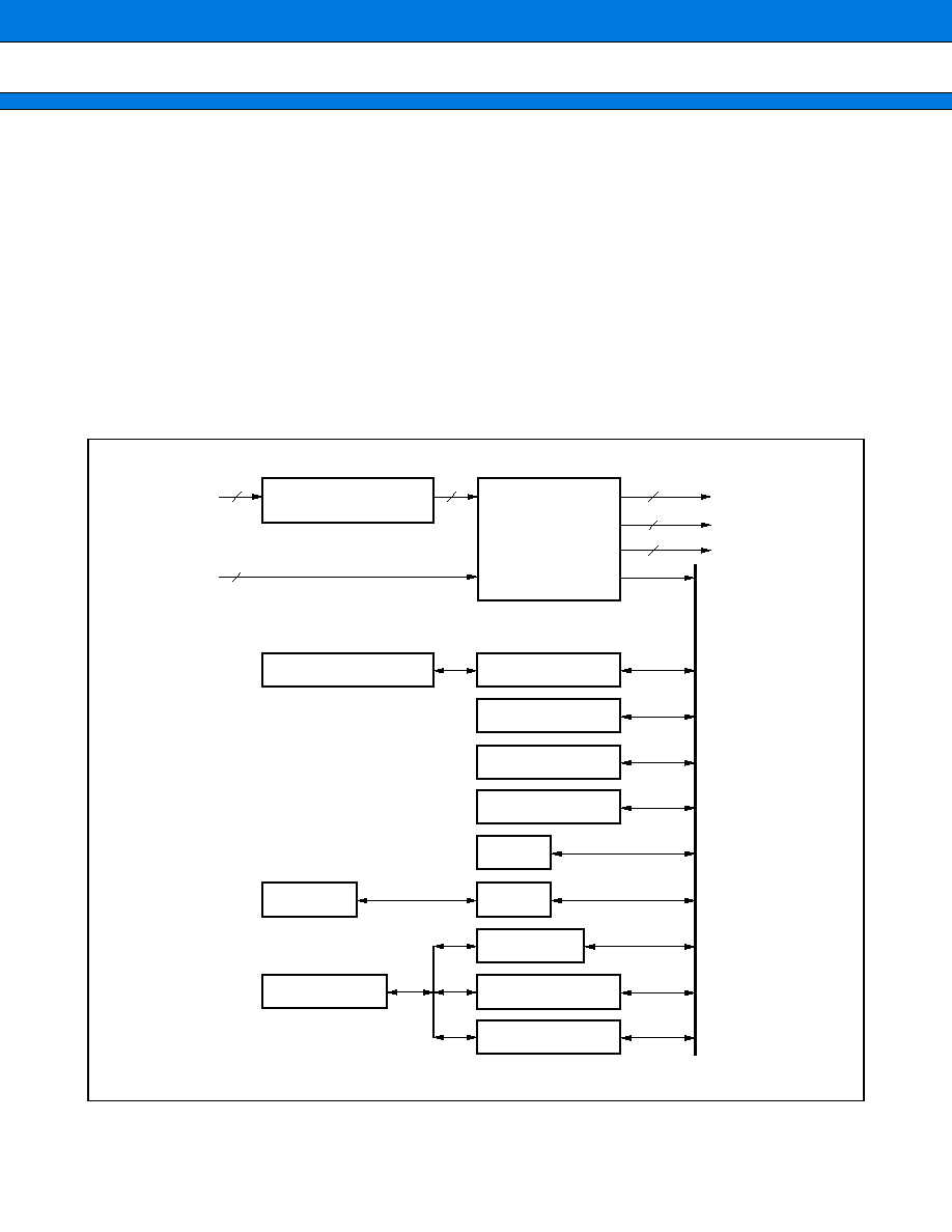
MB91133/MB91F133
82
15. DMA Controller
The DMA controller is the built-in module of the MB91130 series that carrie out direct memory access (DMA)
transfers.
∑ Characteristics of the DMA Controller
∑ 8 channels
∑ 3 transfer mode types : single/block transfer, burst transfer, continuous transfer
∑ Transfer between overall address areas
∑ Maximum 65,536 transfers
∑ Interruption function when transfer ends
∑ Increase/decrease in transfer addresses can be selected using software
∑ 3 external transfer request input/output pins and 3 external transfer end output pins
∑ Block Diagram
DREQ0 to DREQ2
Built-in resource
transfer request
DACK0 to DACK2
EOP0 to EOP2
Interruption request
DPDP
Switcher
DACSR
Data bus
DATCR
BLK DEC
Data buffer
INC / DEC
BLK
Mode
DMACT
SADR
DADR
3
Edge / level
detection circuit
3
Sequencer
3
3
8
5
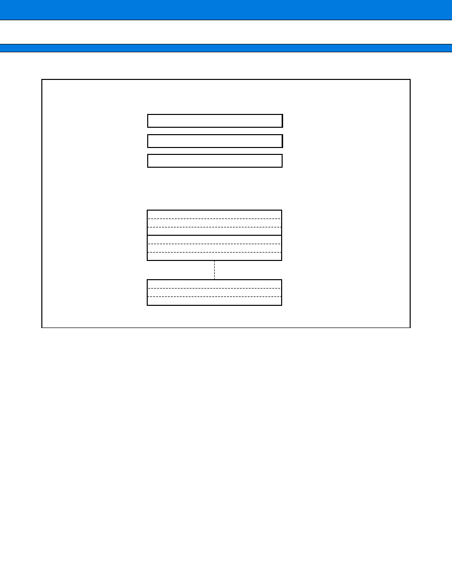
MB91133/MB91F133
83
∑ Register List
(In DMAC : DMAC internal registers)
(On RAM : DMA descriptors)
00000200
H
00000204
H
00000208
H
DPDP
DACSR
DATCR
31
0
bit 31
bit 0
DPDP
+
0
H
DPDP
+
0C
H
DPDP
+
54
H
DMA
ch0
Descriptor
DMA
ch1
Descriptor
DMA
ch7
Descriptor
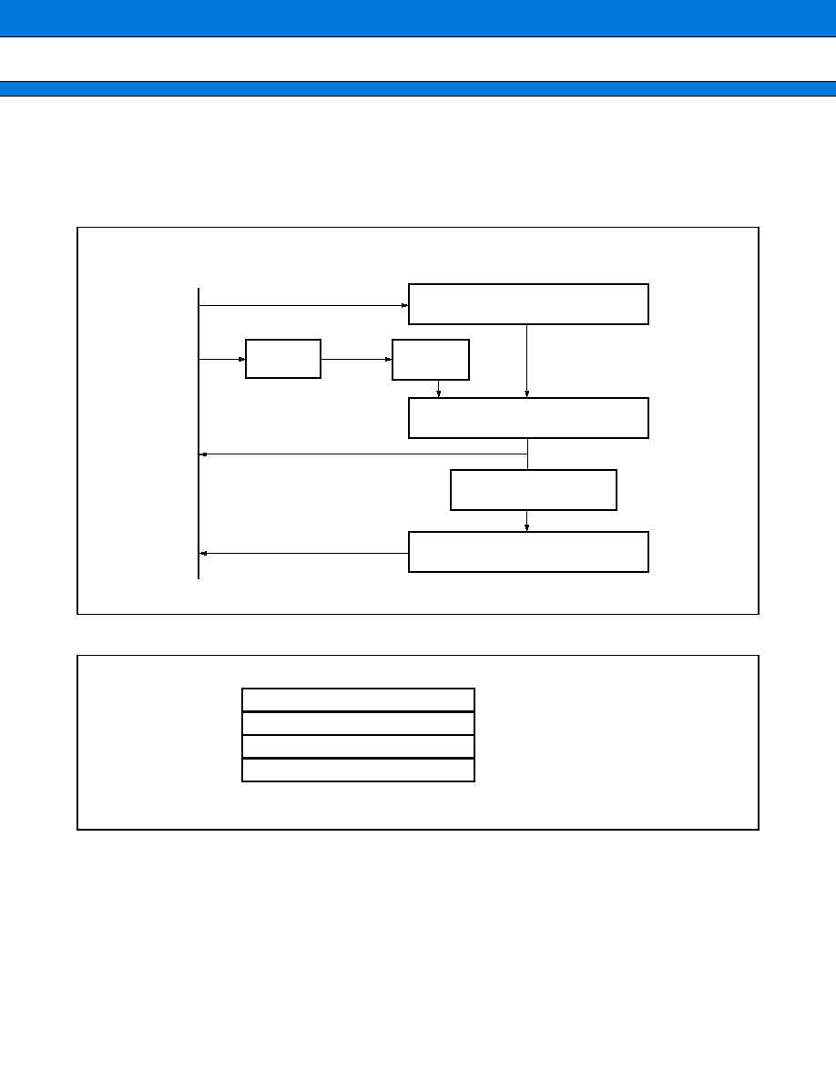
MB91133/MB91F133
84
16. Bit Search Module
The bit search module searches for 0, 1 or change points on data that has been written in the input register, and
returns the detected bit position.
∑ Block Diagram
∑ Register List
D-BUS
Input latch
Changing to 1 detection data
Bit search circuit
Detection results
Address
decoder
Detection
mode
Address :
Data register for 0 detection
Address :
Data register for 1 detection
Address :
Data register for change point detection
Address :
Detection results register
31
BSD0
BSD1
BSDC
BSRR
000003F0
H
000003F4
H
000003F8
H
000003FC
H
0
MB91133/MB91F133
85
17. FLASH Memory
The MB91FV130 / MB91F133 have a 254-KB (2 Mbit) capacity and feature a FLASH memory that can write
each half-word (16 bits) using the FR-CPU, delete individual sectors sector and delete groups of sectors together
using a single 3-V power source.
∑ Outline of FLASH Memory
This is a built-in 3-V 254-KB FLASH memory. This FLASH memory is the same as our 2-Mbit (256 K
◊
8
/
128
K
◊
16) FLASH memory MBM29LV400C and writing is possible from outside the device using a ROM writer. If
used as a built-in ROM of the FR-CPU, as well as having an equivalent function to the MBM29LV400C, instruc-
tions
/
data can be read per word (32 bits) and high-speed operation of the device can be realized.
Refer to the MBM29LV400C data sheet as well as this manual.
The following functions can be realised in MB91FV130 / MB91F133 by combining the FLASH memory macro
and FR-CPU interface circuits.
∑ Functioning as memory for CPU program
/
data storage
Access is possible with 32-bit bus width when used as ROM
Reading
/
writing and erasing (automatic program algorithm
*
) are possible using CPU
∑ MBM29LV400C-equivalent function of single FLASH memory products
Reading
/
writing and erasing (automatic program algorithm
*
) are possible using ROM writer
A case where this FLASH memory is used from FR-CPU is described in this section.
Refer to the ROM writer manual separately for details if this FLASH memory is used from ROM writer.
* : Automatic program algorithm
=
Embedded Algorithm
TM
Embedded Algorithm
TM
is the trademark of Advanced Micro Device.
∑ Block Diagram
RDY/BUSY
RESET
BYTE
OE
WE
CE
FA18 - 0
Address buffer
Data buffer
CA18 - 0
Interruption request
Bus control signal
INTE
RDYINT
RDY
WE
FR-C bus (instruction / data)
Rising edge detection
Control signal
generation
CD31 - 0
DI15 - 0
FLASH memory
2 Mbit (254 K
◊
8/127 K
◊
16)
DO31 - 0
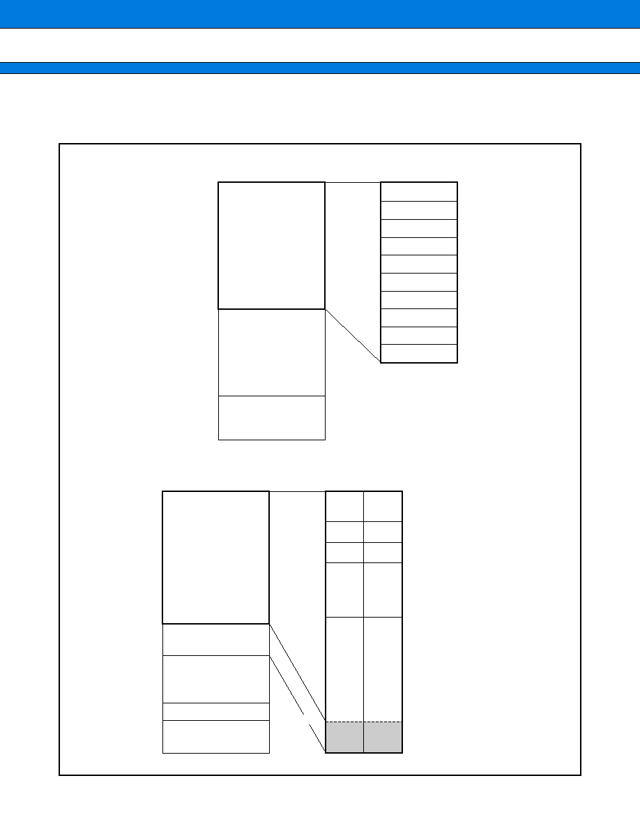
MB91133/MB91F133
86
∑ Memory Map
FLASH memory mode and CPU mode for address mapping of FLASH memory are different. Mapping under
each mode is shown as follows.
∑ Memory map in FLASH memory mode
∑ Memory map in CPU memory mode
SA9
SA8
SA7
SA6
SA5
SA4
SA3
SA2
SA1
SA0
( SAn : sector address n )
2 M-FLASH
Memory image
0FFFFF
H
0C0000
H
010000
H
000000
H
( SAn : sector address n )
CPU mode
0FFFFF
H
0FFFFF
H
SA4
SA9
SA3
SA8
SA2
SA7
SA1
SA6
SA0
FLASH memory area
Status register
RAM area
2 KByte
SA5
0F8000
H
0F4000
H
0F0000
H
0E0000
H
0C0000
H
0C0800
H
0C0000
H
0007C0
H
000000
H
0C0800
H
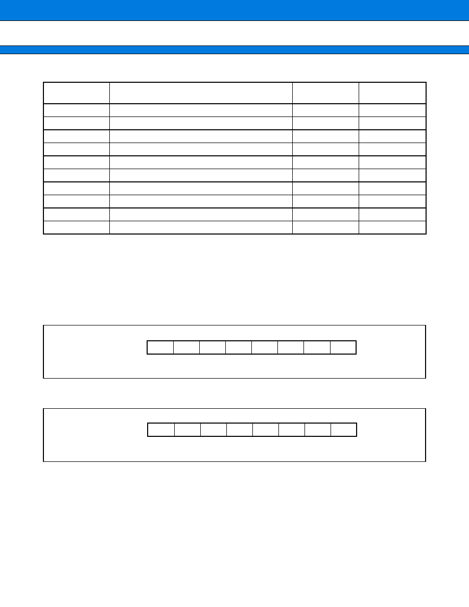
MB91133/MB91F133
87
∑ Sector address table
∑ Registers of FLASH Memory
There are two types of FLASH memory registers, namely status register (FLCL) and wait register (FWTC).
∑ Status Register (FLCR) (CPU mode)
This register indicates the operation status of the FLASH memory. It controls interruption to the CPU and
writing to the FLASH memory.
Access is possible only in CPU mode. This register must not be accessed under Read / Modify / Write
instructions.
∑ Wait Register ( FWTC)
Carries out wait control of the FLASH memory in CPU mode. Also, controls access to high-speed reading
(33MHz) of FLASH memory. Configuration of Wait Register (FWTC) is as follows :
Note : FACH bit should be set to 1 or WTC1/0 should be set to 01b to operate machine clocks of CPUs exceeding
25 MHz.
Sector Address
Address Area
Position of bit
handled
Sector Capacity
SA5
000C0802, 3h to 000DFFFE, Fh (LSB side 16 bit)
bit 15 to 0
63 Kbyte
SA6
000E0002, 3h to 000EFFFE, Fh (LSB side 16 bit)
bit 15 to 0
32 Kbyte
SA7
000F0002, 3h to 000F3FFE, Fh (LSB side 16 bit)
bit 15 to 0
8 Kbyte
SA8
000F4002, 3h to 000F7FFE, Fh (LSB side 16 bit)
bit 15 to 0
8 Kbyte
SA9
000F8002, 3h to 000FFFFE, Fh (LSB side 16 bit)
bit 15 to 0
16 Kbyte
SA0
000C0800, 1h to 000DFFFC, Dh (MSB side 16 bit)
bit 31 to 16
63 Kbyte
SA1
000E0000, 1h to 000EFFFC, Dh (MSB side 16 bit)
bit 31 to 16
32 Kbyte
SA2
000F0000, 1h to 000F3FFC, Dh (MSB side 16 bit)
bit 31 to 16
8 Kbyte
SA3
000F4000, 1h to 000F7FFC, Dh (MSB side 16 bit)
bit 31 to 16
8 Kbyte
SA4
000F8000, 1h to 000FFFFC, Dh (MSB side 16 bit)
bit 31 to 16
16 Kbyte
R/W
( 0 )
R/W
( 0 )
R
( X )
( X )
( X )
( X )
R/W
( 0 )
bit 7
bit 6
bit 5
bit 4
bit 3
bit 2
bit 1
bit 0
RDYINT
R/W
( 0 )
INTE
WE
RDY
LPM
0007C0
H
(
)
(
)
(
)
(
)
W
( 0 )
R/W
( 0 )
R/W
( 0 )
bit 7
bit 6
bit 5
bit 4
bit 3
bit 2
bit 1
bit 0
(
)
FACH
WTC1
WTC0
0007C4
H
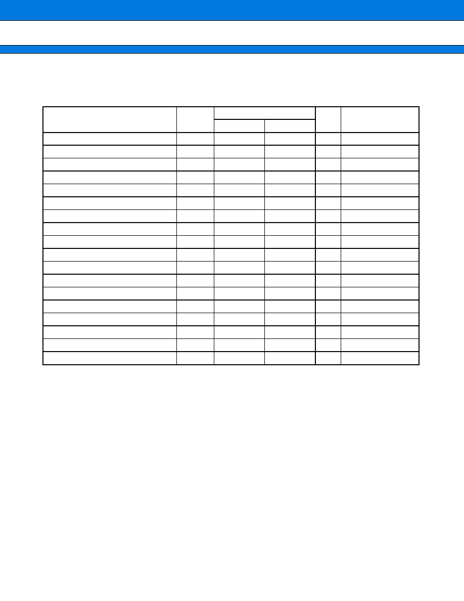
MB91133/MB91F133
88
s
ELECTRICAL CHARACTERISTICS
1.
Absolute Maximum Ratings
(V
SS
=
AV
SS
=
0.0 V)
*1 : Care must be taken that this does not exceed V
CC
5
+
0.3 V when the power is turned on. Also, care must be
taken that AV
CC
does not exceed V
CC
5 when the power is turned on. AV
CC
should be set at the same electrical
potential as V
CC
5.
*2 : Peak value of the pin concerned is regulated as the maximum output current.
*3 : Average current within 100 ms flowing in the pin concerned is regulated as the average output current.
*4 : Average current within 100 ms flowing in all pins concerned is regulated as the average total output current.
WARNING: Semiconductor devices can be permanently damaged by application of stress (voltage, current,
temperature, etc.) in excess of absolute maximum ratings. Do not exceed these ratings.
Parameter
Symbol
Rating
Unit
Remarks
Min.
Max.
Power voltage
V
CC
5
V
SS
-
0.3
V
SS
+
6.5
V
Power voltage
V
CC
3
V
SS
-
0.3
V
SS
+
3.8
V
Analog power voltage
AV
CC
V
SS
-
0.3
V
SS
+
6.5
V
*1
Standard analog voltage
AVRH
V
SS
-
0.3
V
SS
+
6.5
V
*1
Input voltage
V
I5
V
SS
-
0.3
V
CC
5
+
0.3
V
Input voltage
V
I3
V
SS
-
0.3
V
CC
3
+
0.3
V
X0, X1, X0A, X01A
Analog pin input voltage
V
IA
V
SS
-
0.3
AV
CC
+
0.3
V
Output voltage
V
O
V
SS
-
0.3
V
CC
5
+
0.3
V
Maximum "L" level output current
I
OL
10
mA
*2
Average "L" level output current
I
OLAV
4
mA
*3
Maximum total "L" level output current
I
OL
100
mA
Average "L" level total output current
I
OLAV
50
mA
*4
Maximum "H" level output current
I
OH
-
10
mA
*2
Average "H" level output current
I
OHAV
-
4
mA
*3
Maximum total "H" level output current
I
OH
-
50
mA
Average "H" level total output current
I
OHAV
-
20
mA
*4
Electricity consumption
P
D
500
mW
Storage temperature
Tstg
-
55
+
150
∞
C
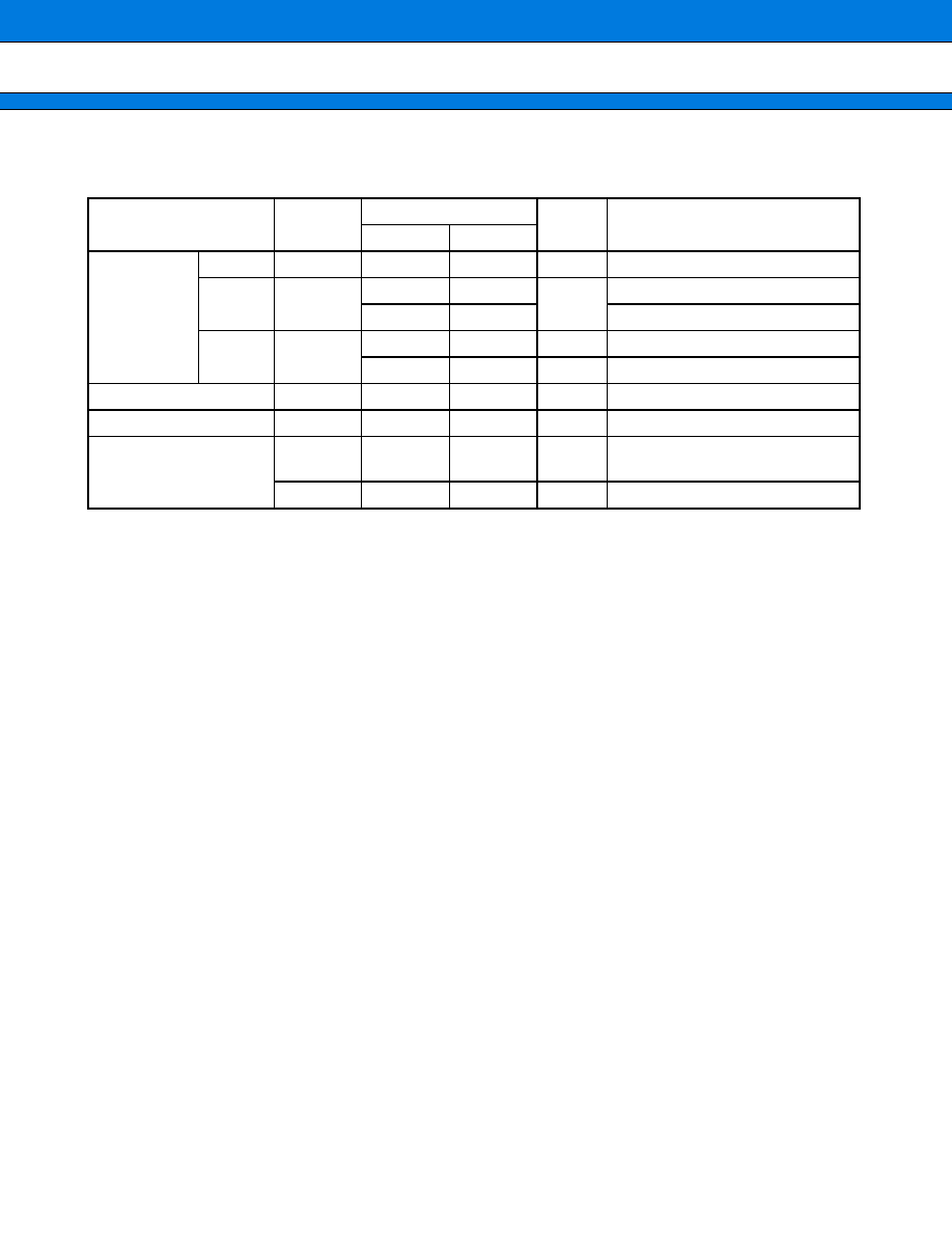
MB91133/MB91F133
89
2.
Recommended Operating Conditions
(V
SS
=
AV
SS
=
0.0 V)
WARNING: The recommended operating conditions are required in order to ensure the normal operation of the
semiconductor device. All of the device's electrical characteristics are warranted when the device is
operated within these ranges.
Always use semiconductor devices within their recommended operating condition ranges. Operation
outside these ranges may adversely affect reliability and could result in device failure.
No warranty is made with respect to uses, operating conditions, or combinations not represented on
the data sheet. Users considering application outside the listed conditions are advised to contact their
FUJITSU representatives beforehand.
Parameter
Symbol
Value
Unit
Remarks
Min.
Max.
Power voltage
Common
V
CC
5
4.5
5.5
V
Under normal operation
EVA
FLASH
V
CC
3
3.0
3.6
V
Under normal operation
3.0
3.6
RAM status kept in the case of stop
MASK
ROM
V
CC
3
2.7
3.6
V
Under normal operation
2.7
3.6
V
RAM status kept in the case of stop
Analog power voltage
AV
CC
V
SS
+
4.5
V
SS
+
5.5
V
Standard analog voltage
AVRH
AV
SS
-
0.3
AV
CC
V
Operating temperature
T
A
0
+
70
∞
C
In external ROM external bus /
internal ROM external bus modes
T
A
-
40
+
70
∞
C
In single-chip mode
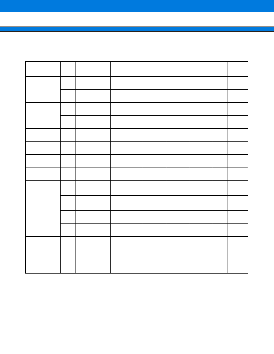
MB91133/MB91F133
90
3.
DC Characteristics
(MASK Model V
CC
5
=
AV
CC
=
DAVC
=
5.0 V
±
10
%
, V
CC
3
=
2.7 V to 3.6 V, V
SS
=
AV
SS
=
0 V, T
A
=
-
40
∞
C to
+
70
∞
C)
(FLASH Model V
CC
5
=
AV
CC
=
DAVC
=
5.0 V
±
10
%
, V
CC
3
=
3.0 V to 3.6 V, V
SS
=
AV
SS
=
0 V, T
A
=
-
40
∞
C to
+
70
∞
C)
*1 : Refer to "PIN FUNCTION DESCRIPTIONS"
*2 : In case of CLK pin output only (C
L
=
80 pF)
*3 : Output pin OPEN
Parameter
Sym-
bol
Pin name
Conditions
Value
Unit
Re-
marks
Min.
Typ.
Max.
"H" level input
voltage
V
IH
Input excluding
following (*1)
0.7 V
CC
5
V
CC
5
+
0.3
V
V
IHS
*1 Hysteresis
input pin
V
CC
5
-
0.4
V
CC
5
+
0.3
V
"L" level input
voltage
V
IL
Input excluding
following (*1)
V
SS
-
0.3
0.2 V
CC
5
V
V
ILS
*1 Hysteresis
input pin
V
SS
-
0.3
V
SS
+
0.4
V
"H" level output
voltage
V
OH
V
CC
5
=
5.0 V,
I
OH
=
-
4.0 mA
2.6
V
"L" level output
voltage
V
OL
V
CC
5
=
5.0 V,
I
OL
=
4.0 mA
0.6
V
Input leak
current
I
LI
V
CC
5
=
5.0 V,
V
SS
<
V
I
<
V
DD
-
5
5
µ
A
Pull up
resistance value
R
PULL
RST
50
k
Power current
I
CC
5
V
CC
5
V
CC
5
=
5.0 V
15
20
mA
*2
I
CC
3
V
CC
3
V
CC
3
=
3.0 V
50
100
mA
I
CCS
5
V
CC
5
V
CC
5
=
5.0 V
15
20
mA
*2
I
CCS
3
V
CC
3
V
CC
3
=
3.0 V
24
85
mA
I
CCH
5
V
CC
5
V
CC
5
=
5.0 V,
T
A
=
25
∞
C
10
100
µ
A
*3
I
CCH
3
V
CC
3
V
CC
3
=
3.0 V,
T
A
=
25
∞
C
10
100
µ
A
Power current
(FLASH
models)
I
CC
3
V
CC
3
V
CC
3
=
3.3 V
80
120
mA
I
CCS
3
V
CC
3
V
CC
3
=
3.3 V
50
90
mA
Input capacity
C
IN
Other than V
CC
,
AV
CC
, AV
SS
,
AV
RH
and V
SS
10
pF
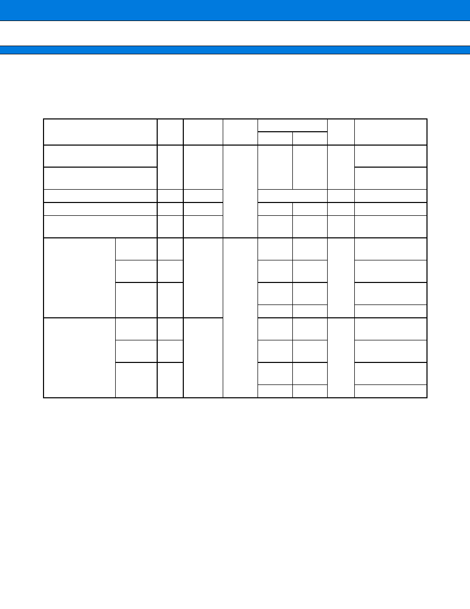
MB91133/MB91F133
91
4.
AC Characteristics
(1) Clock Timing Standard
(MASK Model V
CC
5
=
AV
CC
=
DAVC
=
5.0 V
±
10
%
, V
CC
3
=
2.7 V to 3.6 V, V
SS
=
AV
SS
=
0 V, T
A
=
-
40
∞
C to
+
70
∞
C)
(FLASH Model V
CC
5
=
AV
CC
=
DAVC
=
5.0 V
±
10
%
, V
CC
3
=
3.0 V to 3.6 V, V
SS
=
AV
SS
=
0 V, T
A
=
-
40
∞
C to
+
70
∞
C)
*1 : Frequency fluctuation rate indicates the maximum fluctuation ratio from the setting central frequency during
locking in case of doubling.
*2 : The targeted analog areas are the A/D and level comparator.
Parameter
Sym-
bol
Pin name
Condi-
tions
Value
Unit
Remarks
Min.
Max.
Clock frequency
(high-speed, self-oscillation)
f
C
X0, X1
9
16.5
MHz
Self oscillation
available area
Clock frequency
(high-speed, PLL usage)
PLL usable area by
self-oscillation input
Clock frequency (low-speed)
f
CA
X0A, X1A
32
kHz
Self oscillation
Clock cycle time
t
C
30.3
31250
ns
Frequency fluctuation rate
*1
(when PLL locked)
f
10
%
Internal operation
clock frequency
CPU
system
f
CP
0.032
33
MHz
Bus
system
f
CPB
0.032
25
Peripheral
system
f
CPP
0.032
25
Excluding analog
area
*2
1
25
Analog area
*2
Internal operation
clock cycle time
CPU
system
t
CP
30.3
31250
ns
Bus
system
t
CPB
40
31250
Peripheral
system
t
CPP
40
31250
Excluding analog
area
*2
40
1000
Analog area
*2
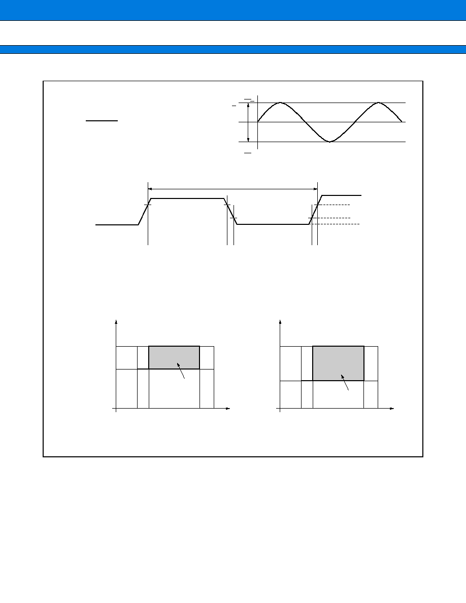
MB91133/MB91F133
92
-
-
Central frequency f
O
t
C
V
CC
3
V
SS
0.8 V
CC
3
0.2 V
CC
3
f
=
◊
100 (
%
)
|
|
f
O
V
CC
3
3.6
3.0
f
CPP
f
CP
1 M
Frequency (Hz)
Guaranteed operating range
Power voltage (V)
33 M
32 K
25 M
Peripheral system clock setting permitted area (A/D, D/A level comparator : 5 V
±
10
%
)
< FLASH model >
V
CC
3
3.6
2.7
f
CPP
f
CP
1 M
33 M
32 K
25 M
Frequency (Hz)
Guaranteed operating range
Power voltage (V)
< MASK ROM model >
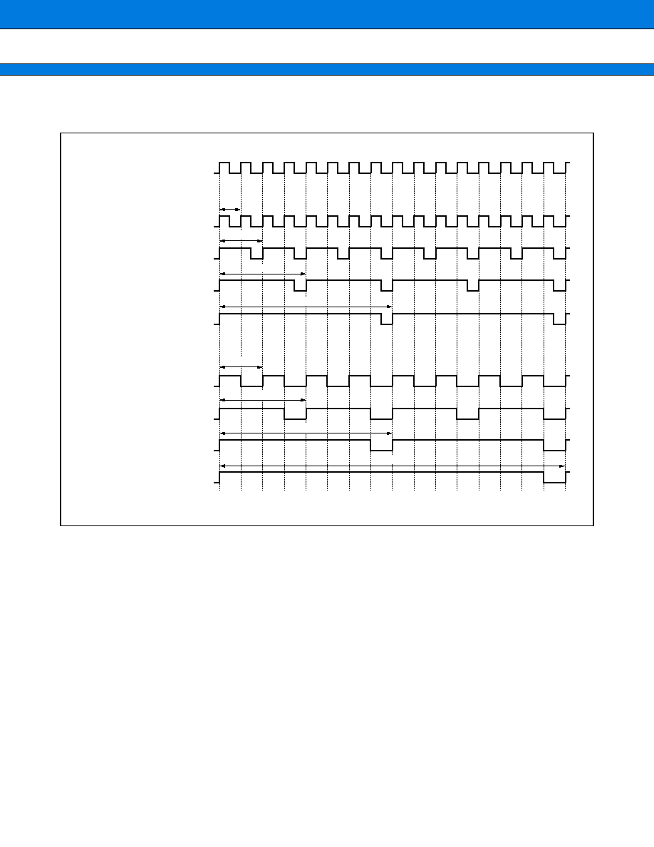
MB91133/MB91F133
93
The relationship between the internal clock set by the CHC/CCK1/CCK0 bit of the Gear Control Register (GCR)
and X0 input is as follows.
t
CYC
t
CYC
t
CYC
t
CYC
t
CYC
t
CYC
t
CYC
t
CYC
X0 input
∑
Original oscillation
◊
1
(CHC bit of GCR : 0 setting)
(a) Gear
◊
1 Internal clock
CCK1/0 : 00
(b) Gear
◊
1/2 Internal clock
CCK1/0 : 01
(c) Gear
◊
1/4 Internal clock
CCK1/0 : 10
(d) Gear
◊
1/8 Internal clock
CCK1/0 : 11
∑
Original oscillation
◊
1/2
(CHC bit of GCR : 1 setting)
(a) Gear
◊
1 Internal clock
CCK1/0 : 00
(b) Gear
◊
1/2 Internal clock
CCK1/0 : 01
(c) Gear
◊
1/4 Internal clock
CCK1/0 : 10
(d) Gear
◊
1/8 Internal clock
CCK1/0 : 11
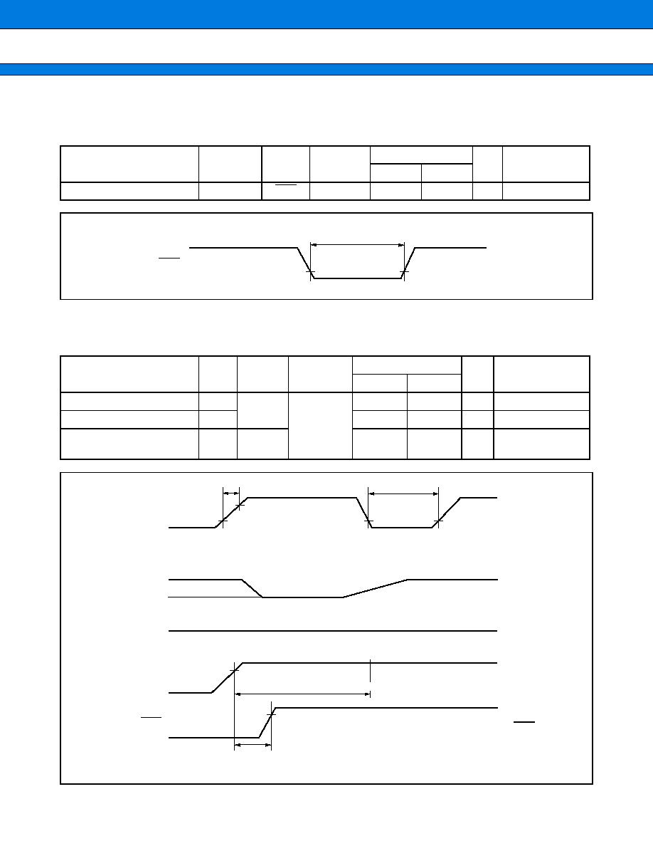
MB91133/MB91F133
94
(2) Reset Input Standards
(MASK Model V
CC
5
=
AV
CC
=
DAVC
=
5.0 V
±
10
%
, V
CC
3
=
2.7 V to 3.6 V, V
SS
=
AV
SS
=
0 V, T
A
=
-
40
∞
C to
+
70
∞
C)
(FLASH Model V
CC
5
=
AV
CC
=
DAVC
=
5.0 V
±
10
%
, V
CC
3
=
3.0 V to 3.6 V, V
SS
=
AV
SS
=
0 V, T
A
=
-
40
∞
C to
+
70
∞
C)
(3) Power On Reset
(MASK Model V
CC
5
=
AV
CC
=
DAVC
=
5.0 V
±
10
%
, V
CC
3
=
2.7 V to 3.6 V, V
SS
=
AV
SS
=
0 V, T
A
=
-
40
∞
C to
+
70
∞
C)
(FLASH Model V
CC
5
=
AV
CC
=
DAVC
=
5.0 V
±
10
%
, V
CC
3
=
3.0 V to 3.6 V, V
SS
=
AV
SS
=
0 V, T
A
=
-
40
∞
C to
+
70
∞
C)
Parameter
Symbol
Pin
name
Condi-
tions
Value
Unit
Remarks
Min.
Max.
Reset input time
t
RSTL
RST
t
CP
◊
5
ns
Parameter
Sym-
bol
Pin
name
Conditions
Value
Unit
Remarks
Min.
Max.
Power startup time
f
R
V
CC
20
ms
Power cut time
t
OFF
2
ms
Waiting time for oscillation
stabilization
t
OSC
2
13
t
C
ns
RST
t
RSTL
0.2 V
CC
V
hhR
t
R
0.9
◊
V
CC
3
0.2 V
t
OFF
V
CC
V
SS
V
CC
RST
t
RSTL
Holding RAM data
t
OSC
(waiting for oscillation stabilization)
If the power voltage is changed rapidly, "Power On Reset" may be initiated. To start up smoothly,
controlling any voltage fluctuations that may occur during operation is recommended.
Controling inclination at initiation to 50
mV/ms or less is recommended.
When power is turned on, start while the RST pin
is set to "L" level, after which wait for t
RSTL
minutes
and change the level to "H" once the V
CC
power
level is reached.
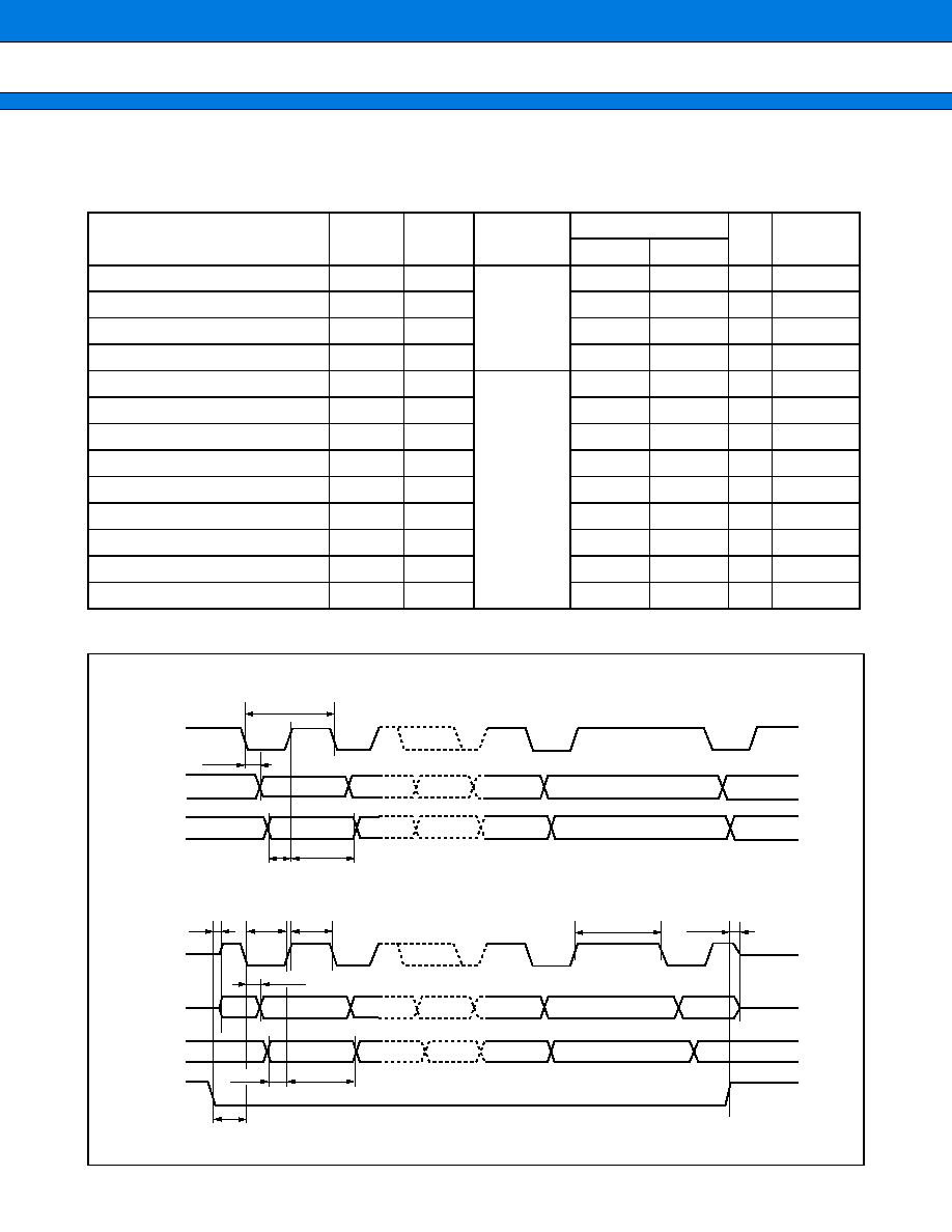
MB91133/MB91F133
95
(4) Serial I/O (CH0 to 4)
(MASK Model V
CC
5
=
AV
CC
=
DAVC
=
5.0 V
±
10
%
, V
CC
3
=
2.7 V to 3.6 V, V
SS
=
AV
SS
=
0 V, T
A
=
-
40
∞
C to
+
70
∞
C)
(FLASH Model V
CC
5
=
AV
CC
=
DAVC
=
5.0 V
±
10
%
, V
CC
3
=
3.0 V to 3.6 V, V
SS
=
AV
SS
=
0 V, T
A
=
-
40
∞
C to
+
70
∞
C)
*: Will be Min. 1 t
CPP
-
10 if pre-scalar setting is CS2, 1, 0
=
000.
Parameter
Symbol
Pin
name
Conditions
Value
Unit
Remarks
Min.
Max.
Serial clock cycle time
t
SCYC
Internal
clock
8 t
CPP
ns
SCK
SO delay time
t
SLOV
-
10
50
ns
Valid SI
SCK
t
IVSH
50
ns
SCK
Valid SI holding time
t
SHIX
50
ns
Serial clock H pulse width
t
SHSL
External
clock
4 t
CPP
-
10
ns
*
Serial clock L pulse width
t
SLSH
4 t
CPP
-
10
ns
SCK
SO delay time
t
SLOV
0
50
ns
Valid SI
SCK
t
IVSH
50
ns
SCK
Valid SI holding time
t
SHIX
50
ns
Serial busy period
t
BUSY
6 t
CPP
ns
SCS
SCK, SO delay time
t
CLZO
50
ns
SCS
SCK input MASK time
t
CLSL
3 t
CPP
ns
SCS
SCK, SO Hi-Z time
t
CHOZ
50
ns
Internal shift clock mode
External shift clock mode
SCK
SO
SI
t
SHIX
t
IVSH
t
SLOV
t
SCYC
SCK
SO
SI
SCS
t
CHOZ
t
BUSY
t
CLSL
t
IVSH
t
SHIX
t
SLOV
t
SLSH
t
CLZO
t
SHSL
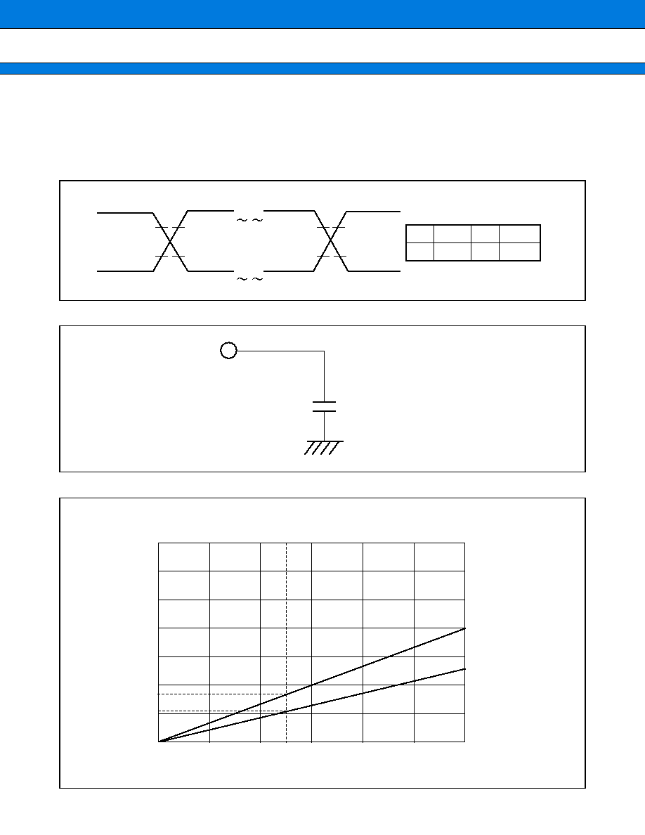
MB91133/MB91F133
96
(5) External Bus Measurement Conditions
The following conditions apply to items without specific regulations.
∑ Alternating current standard measurement condition
V
CC
: 5.0 V
±
10
%
∑ Load condition
∑ Load capacity
-
Delay time characteristic (Internally-based output delay)
V
IH
V
IL
V
OH
V
OL
V
CC
Input
Output
0 V
(Rise/fall time of input is 10 ns or less)
V
IH
2.4 V
V
OH
2.4V
V
IL
0.8 V
V
OL
0.8V
C
=
50 pF
( V
CC
: 5.0 V
±
10% )
Output pin
[nS]
35
30
25
20
15
10
5
0
0
20
40
50
60
80
100
120
C[pF]
5 V Rise
5 V Fall
MB91133/MB91F133
97
(6) Normal Bus Access Read/Write Operation
(MASK Model V
CC
5
=
AV
CC
=
DAVC
=
5.0 V
±
10
%
, V
CC
3
=
2.7 V to 3.6 V, V
SS
=
AV
SS
=
0 V, T
A
=
-
40
∞
C to
+
70
∞
C)
(FLASH Model V
CC
5
=
AV
CC
=
DAVC
=
5.0 V
±
10
%
, V
CC
3
=
3.0 V to 3.6 V, V
SS
=
AV
SS
=
0 V, T
A
=
-
40
∞
C to
+
70
∞
C)
*1 : Time (t
CYC
◊
number of cycles extended) needs to be added to this standard if the bus is extended by automatic
waiting insertion and RDY input.
*2 : Values of this standard are in case of gear cycle
◊
1.
If the gear cycle is set to 1/2, 1/4 or 1/8, calculation should be made using the following formula and replacing
n with 1/2, 1/4 or 1/8.
∑
Calculation formula : (2
-
n
/
2)
◊
t
CYC
-
25
Parameter
Sym-
bol
Pin name
Conditions
Value
Unit
Remarks
Min.
Max.
Address delay time
t
CHAV
CLK
A23 to A00
15
ns
Data delay time
t
CHDV
CLK
D31 to D16
15
ns
RD delay time
t
CLRL
CLK
RD
10
ns
RD delay time
t
CLRH
10
ns
WR0 to 1 delay time
t
CLWL
CLK
WR0 to 1
10
ns
WR0 to 1 delay time
t
CLWH
10
ns
Valid address
/
valid data input time
t
AVDV
A23 to A00
D31 to D16
3
/
2
◊
t
CYC
-
25
ns
*1, *2
RD
valid data input time
t
RLDV
RD
D31 to D16
t
CYC
-
15
ns
*1
Data setup
RD
time
t
DSRH
15
ns
RD
Data holding time
t
RHDX
0
ns
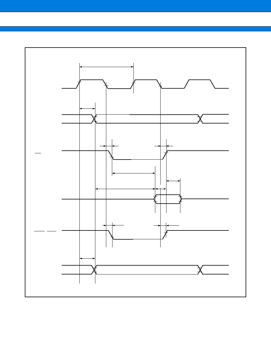
MB91133/MB91F133
98
t
CYC
t
CHAV
t
CLRL
t
CLRH
t
RLDV
t
AVDV
t
RHDX
BA1
BA2
V
OH
V
OL
V
OH
V
OL
V
OH
V
OL
V
OH
V
OL
V
OL
V
IL
V
IH
Read
Write
V
IL
V
IH
V
OH
t
DSRH
V
OH
V
OL
V
OH
V
OL
V
OH
V
OL
t
CLWH
t
CLWL
t
CHDV
CLK
A24 - A00
RD
D31 - D16
WR0 - WR1
D31 - D16
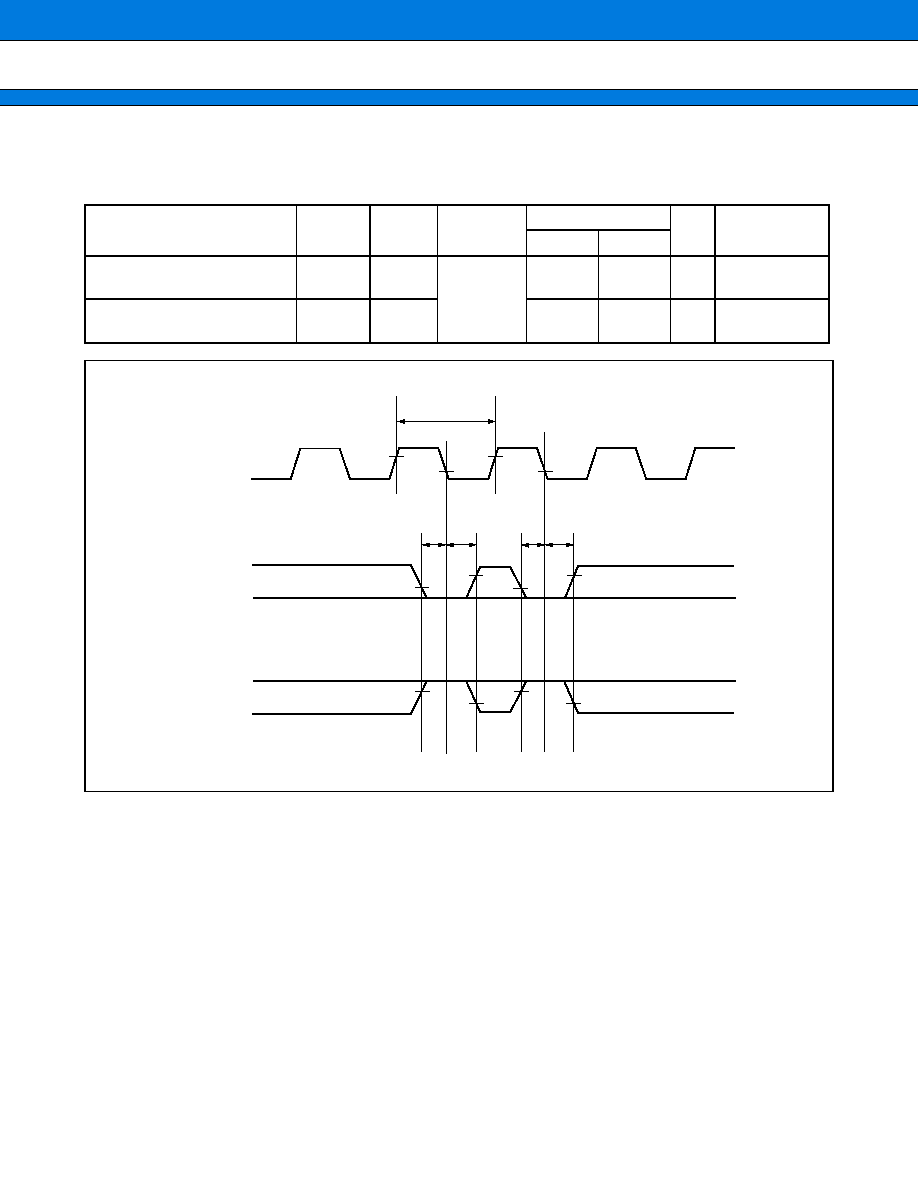
MB91133/MB91F133
99
(7) Ready Input Timing
(MASK Model V
CC
5
=
AV
CC
=
DAVC
=
5.0 V
±
10
%
, V
CC
3
=
2.7 V to 3.6 V, V
SS
=
AV
SS
=
0 V, T
A
=
-
40
∞
C to
+
70
∞
C)
(FLASH Model V
CC
5
=
AV
CC
=
DAVC
=
5.0 V
±
10
%
, V
CC
3
=
3.0 V to 3.6 V, V
SS
=
AV
SS
=
0 V, T
A
=
-
40
∞
C to
+
70
∞
C)
Parameter
Symbol
Pin
name
Conditions
Value
Unit
Remarks
Min.
Max.
RDY setup time
CLK
t
RDYS
RDY
CLK
15
ns
CLK
RDY holding time
t
RDYH
RDY
CLK
0
ns
CLK
RDY
If "wait" is
executed
RDY
If "wait" is
not executed
V
IH
V
IL
V
OH
V
OH
V
OL
V
OL
V
IH
V
IL
t
RDYH
t
RDYS
t
RDYH
t
RDYS
t
CYC
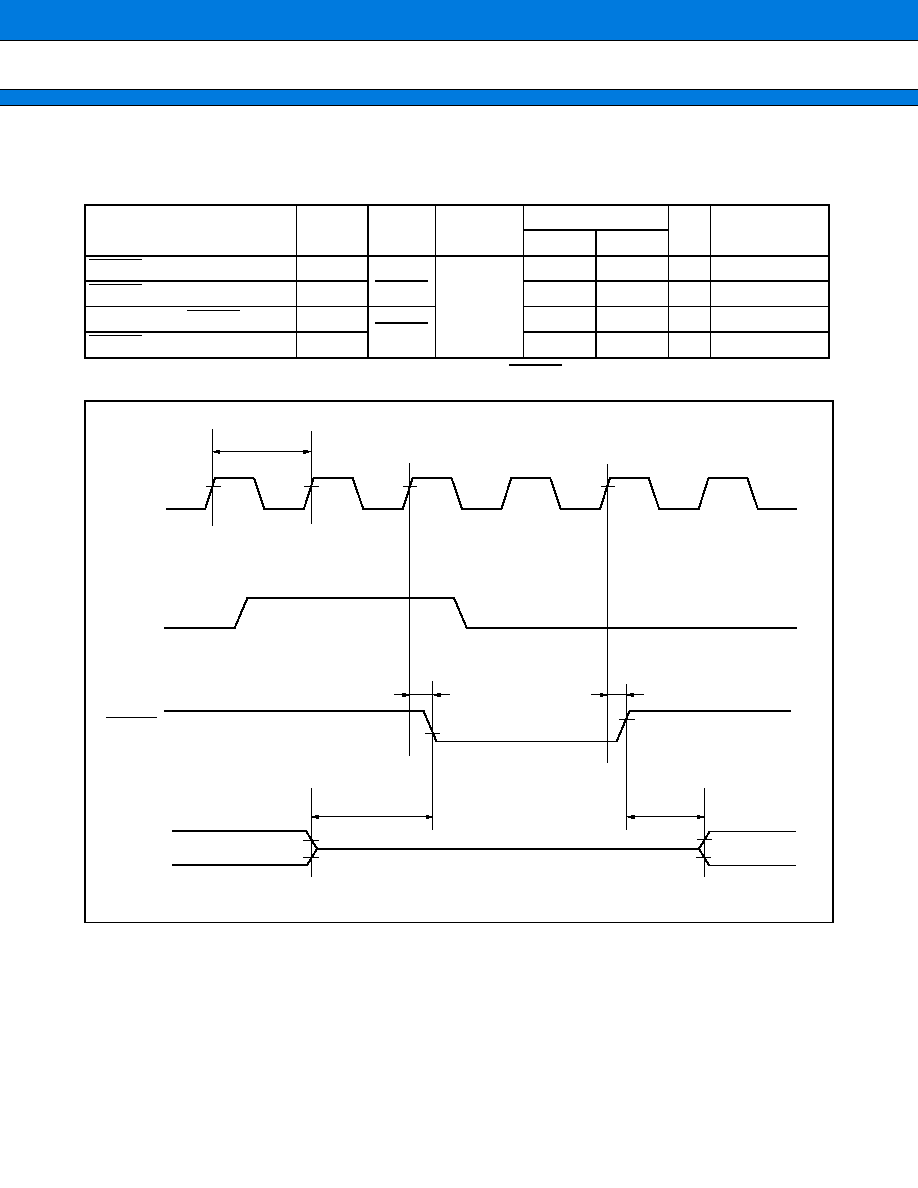
MB91133/MB91F133
100
(8) Holding timing
(MASK Model V
CC
5
=
AV
CC
=
DAVC
=
5.0 V
±
10
%
, V
CC
3
=
2.7 V to 3.6 V, V
SS
=
AV
SS
=
0 V, T
A
=
-
40
∞
C to
+
70
∞
C)
(FLASH Model V
CC
5
=
AV
CC
=
DAVC
=
5.0 V
±
10
%
, V
CC
3
=
3.0 V to 3.6 V, V
SS
=
AV
SS
=
0 V, T
A
=
-
40
∞
C to
+
70
∞
C)
Note : It takes at least one cycle from loading the BRQ to when BGRNT is changed.
Parameter
Symbol
Pin
name
Conditions
Value
Unit
Remarks
Min.
Max.
BGRNT delay time
t
CHBGL
CLK
BGRNT
6
ns
BGRNT delay time
t
CHBGH
6
ns
Pin floating
BGRNT
time
t
XHAL
BGRNT
t
CYC
-
10
t
CYC
+
10
ns
BGRNT
Pin valid time
t
HAHV
t
CYC
-
10
t
CYC
+
10
ns
V
OL
V
OH
t
CHBGL
t
XHAL
High impedance
t
HAHV
t
CHBGH
tcyc
BRQ
BGRNT
Each pin
CLK
V
OH
V
OH
V
OH
V
OH
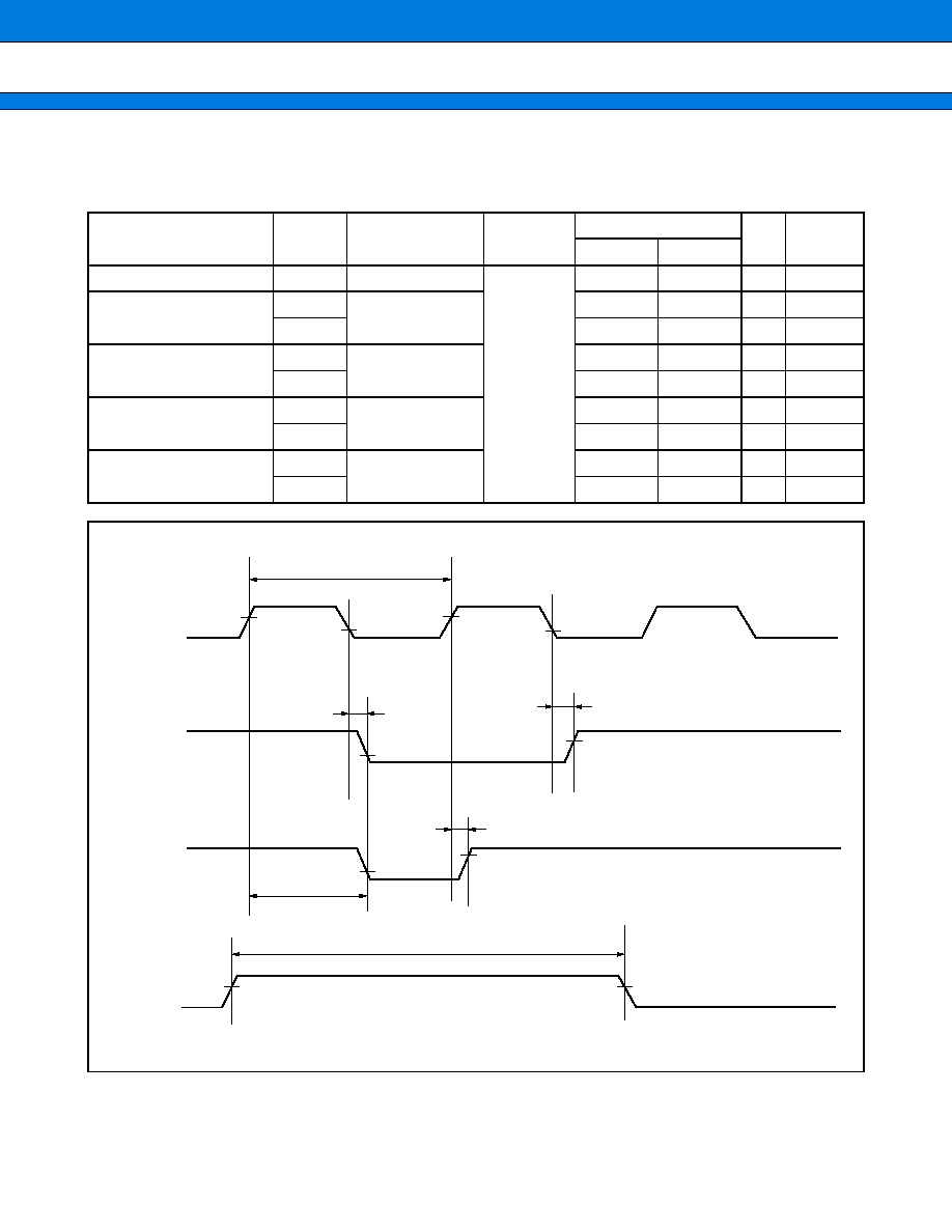
MB91133/MB91F133
101
(9) DMA Controller Timing
(MASK Model V
CC
5
=
AV
CC
=
DAVC
=
5.0 V
±
10
%
, V
CC
3
=
2.7 V to 3.6 V, V
SS
=
AV
SS
=
0 V, T
A
=
-
40
∞
C to
+
70
∞
C)
(FLASH Model V
CC
5
=
AV
CC
=
DAVC
=
5.0 V
±
10
%
, V
CC
3
=
3.0 V to 3.6 V, V
SS
=
AV
SS
=
0 V, T
A
=
-
40
∞
C to
+
70
∞
C)
Parameter
Symbol
Pin name
Conditions
Value
Unit Remarks
Min.
Max.
DREQ input pulse width
t
DRWH
DREQ0 to DREQ2
2 t
CYC
ns
DACK delay time
(Normal bus)
t
CLDL
CLK
DACK0 to DACK2
6
ns
t
CLDH
6
ns
EOP delay time
(Normal bus)
t
CLEL
CLK
EOP0 to EOP2
6
ns
t
CLEH
6
ns
DACK delay time
t
CHDL
CLK
DACK0 to DACK2
n
/
2
◊
t
CYC
ns
t
CHDH
6
ns
EOP delay time
t
CHEL
CLK
EOP0 to EOP2
n
/
2
◊
t
CYC
ns
t
CHEH
6
ns
CLK
V
OL
V
OL
V
OH
V
OH
V
IH
V
IH
t
CLEL
t
CLDL
t
CLEH
t
CLDH
t
CHDH
t
CHDL
t
CHEL
t
DRWH
V
OH
V
OL
V
OL
V
OH
tcyc
DACK0 - 2
EOP0 - 2
(Normal bus)
DACK0 - 2
EOP0 - 2
DREQ0 - 2
MB91133/MB91F133
102
5.
A/D Transition
(MASK Model V
CC
5
=
AV
CC
=
DAVC
=
5.0 V
±
10
%
, V
CC
3
=
2.7 V to 3.6 V, V
SS
=
AV
SS
=
0 V, T
A
=
-
40
∞
C to
+
70
∞
C)
(FLASH Model V
CC
5
=
AV
CC
=
DAVC
=
5.0 V
±
10
%
, V
CC
3
=
3.0 V to 3.6 V, V
SS
=
AV
SS
=
0 V, T
A
=
-
40
∞
C to
+
70
∞
C)
Notes :
∑
As the |AV
RH
| becomes smaller, the tolerance becomes larger.
∑
Output impedance of external circuits other than analog input must be used if output impedance of external
circuits
<
approx. 7 k
If the output impedance of the external circuits is too high, the sampling time for the analog voltage may
be insufficient.
(Sampling time
=
1.6
µ
s at 33 MHz)
Parameter
Sym-
bol
Pin
name
Conditions
Value
Unit
Re-
marks
Min.
Typ.
Max.
Resolution
10
Bit
Conversion time
5.0
µ
s
Total tolerance
AV
CC
=
5.0 V,
AV
RH
=
5.0 V
-
4.0
4.0
LSB
Straight-line tolerance
-
3.5
3.5
LSB
Differential straight-line
tolerance
-
2.0
2.0
LSB
Zero transition tolerance
V
OT
AN0 to
AN7
AV
CC
=
5.0 V,
AV
RH
=
5.0 V
AV
SS
-
1.5 AV
SS
+
0.5 AV
SS
+
2.5 LSB
Full-scale transition
tolerance
V
FST
AN0 to
AN7
AV
RH
-
5.5 AV
RH
-
1.5 AV
RH
+
0.5 LSB
Analog input current
I
AIN
AN0 to
AN7
0.1
10
µ
A
Analog input voltage
V
AIN
AN0 to
AN7
AV
SS
AV
RH
V
Standard voltage
AV
RH
AV
RH
AV
CC
V
Power
current
When conversion
is activated
I
A
AV
CC
AV
CC
=
5.0 V
3.0
5.0
mA
When conversion
is stopped
I
AH
5.0
µ
A
Standard
voltage
current
supplied
When conversion
is activated
I
R
AV
RH
AV
CC
=
5.0 V,
AV
RH
=
5.0V
2.0
3.0
mA
When conversion
is stopped
I
RH
10
µ
A
Tolerance between
channels
AN0 to
AN7
4
LSB
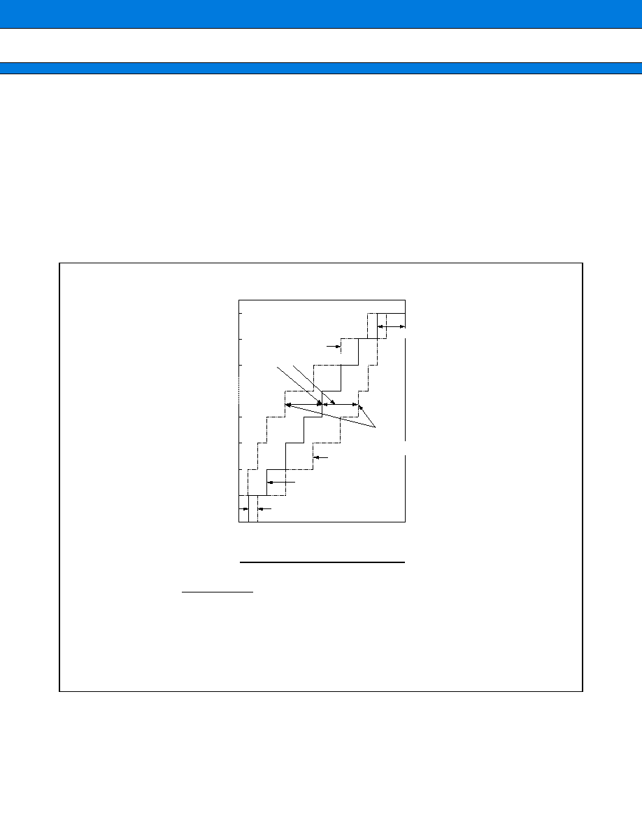
MB91133/MB91F133
103
∑ Definition of A/D Converter Terms
∑ Resolution :
Analog changes that can be identified by A/D converter
∑ Straight-line tolerance :
Difference between the straight line linking the zero transition point (00 0000 0000
00 0000 0001) to the
full-scale transition point (11 1111 1110
11 1111 1111) and actual conversion characteristics.
∑ Differential straight-line tolerance :
Difference compared to the ideal input voltage value required to change the output code 1 LSB
∑ Total tolerance :
Indicates the difference between the actual and theoretical values and includes zero transition tolerance, full-
scale transition tolerance, and straight-line tolerance.
(Continued)
3FF
3FE
3FD
004
003
002
001
AV
SS
AVRH
Analog input
0.5 LSB
{
1 LSB ( N
-
1 )
+
0.5 LSB
}
1.5 LSB
Ideal characteristics
Actual conversion
characteristics
Actual conversion
characteristics
Digital output
V
NT
(Actual
measured value)
Total tolerance
Total tolerance of digital output N
=
V
NT
-
{1 LSB
◊
(N
-
1)
+
0.5 LSB'}
1 LSB
1 LSB (Ideal value)
=
AVRH
-
AV
SS
1024
[V]
V
OT
(Ideal value)
=
AV
SS
+
0.5 LSB'
V
NT
: Voltage of digital output transferred from (N
+
1) to N
[V]
V
FST
(Ideal value)
=
AVRH
-
1.5 LSB' [V]
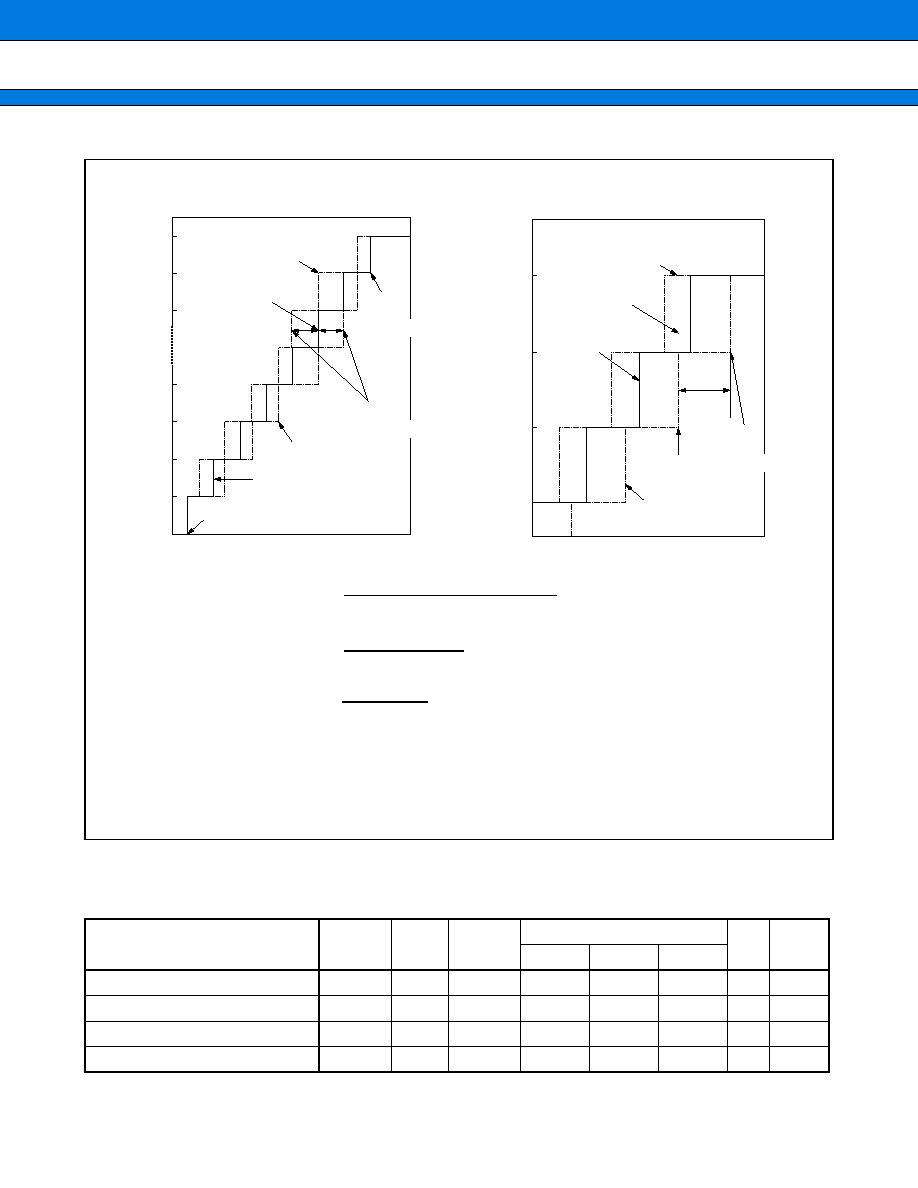
MB91133/MB91F133
104
(Continued)
6.
D/A Transition
(MASK Model V
CC
5
=
AV
CC
=
DAVC
=
5.0 V
±
10
%
, V
CC
3
=
2.7 V to 3.6 V, V
SS
=
AV
SS
=
0 V, T
A
=
-
40
∞
C to
+
70
∞
C)
(FLASH Model V
CC
5
=
AV
CC
=
DAVC
=
5.0 V
±
10
%
, V
CC
3
=
3.0 V to 3.6 V, V
SS
=
AV
SS
=
0 V, T
A
=
-
40
∞
C to
+
70
∞
C)
*: CL
=
20 PF
Parameter
Symbol
Pin
name
Condi-
tions
Value
Unit
Re-
marks
Min.
Typ.
Max.
Resolution
8
Bit
Differential straight-line tolerance
±
0.9
LSB
Conversion time
10
20
µ
s
*
Analog output impedance
28
k
Straight-line tolerance
of digital output N
=
V
NT
-
{1 LSB
◊
(N
-
1)
+
V
OT
}
1 LSB
[LSB]
Differential straight-line tolerance
of digital output N
=
V (
N
+
1
)
T
-
V
NT
1 LSB
-
1
1LSB (Ideal value)
=
V
FST
-
V
OT
1022
[V]
V
OT
: Voltage with digital output transferred from (000)
H
to (001)
H
V
FST
: Voltage with digital output transferred from (3FE)
H
to (3FF)
H
[LSB]
3FF
3FE
3FD
004
003
002
001
AV
SS
AVRH
{
1 LSB ( N
-
1 )
+
V
OT
}
Analog input
Ideal characteristics
Actual conversion
characteristics
Actual conversion
characteristics
Digital output
V
NT
(Actual
measured value)
V
FST
(Actual
measured
value)
V
OT
(Actual measured value)
N
+
1
N
N
-
1
N
-
2
AV
SS
AVRH
Analog input
Ideal characteristics
Actual conversion
characteristics
Actual conversion
characteristics
Digital output
V
NT
(Actual
measured value)
V
FST
(Actual
measured
value)
Straight-line tolerance
Differential straight-line tolerance
MB91133/MB91F133
105
s
s
s
s
INSTRUCTIONS (165 INSTRUCTIONS)
1.
How to Read Instruction Set Summary
(1) Names of instructions
Instructions marked with * are not included in CPU specifications. These are extended instruction codes
added/extended at assembly language levels.
(2) Addressing modes specified as operands are listed in symbols.
Refer to "2. Addressing mode symbols" for further information.
(3) Instruction types
(4) Hexa-decimal expressions of instructions
(5) The number of machine cycles needed for execution
a: Memory access cycle and it has possibility of delay by Ready function.
b: Memory access cycle and it has possibility of delay by Ready function.
If an object register in a LD operation is referenced by an immediately following instruction, the interlock
function is activated and number of cycles needed for execution increases.
c: If an immediately following instruction operates to an object of R15, SSP or USP in read/write mode or
if the instruction belongs to instruction format A group, the interlock function is activated and number of
cycles needed for execution increases by 1 to make the total number of 2 cycles needed.
d: If an immediately following instruction refers to MDH/MDL, the interlock function is activated and number
of cycles needed for execution increases by 1 to make the total number of 2 cycles needed.
For a, b, c and d, minimum execution cycle is 1.
(6) Change in flag sign
∑ Flag change
C : Change
≠ : No change
0 : Clear
1 : Set
∑ Flag meanings
N : Negative flag
Z : Zero flag
V : Over flag
C : Carry flag
(7) Operation carried out by instruction
Mnemonic
Type
OP
CYC
NZVC
Operation
Remarks
ADD
Rj,
Ri
* ADD
#s5,
Ri
,
,
A
C
,
,
A6
A4
,
,
1
1
,
,
CCCC
CCCC
,
,
Ri + Rj
Ri
Ri + s5
Ri
,
,
(1)
(2)
(3)
(4)
(5)
(6)
(7)

MB91133/MB91F133
106
2. Addressing Mode Symbols
Ri
: Register direct (R0 to R15, AC, FP, SP)
Rj
: Register direct (R0 to R15, AC, FP, SP)
R13
: Register direct (R13, AC)
Ps
: Register direct (Program status register)
Rs
: Register direct (TBR, RP, SSP, USP, MDH, MDL)
CRi
: Register direct (CR0 to CR15)
CRj
: Register direct (CR0 to CR15)
#i8
: Unsigned 8-bit immediate (≠128 to 255)
Note: ≠128 to ≠1 are interpreted as 128 to 255
#i20
: Unsigned 20-bit immediate (≠0X80000 to 0XFFFFF)
Note: ≠0X7FFFF to ≠1 are interpreted as 0X7FFFF to 0XFFFFF
#i32
: Unsigned 32-bit immediate (≠0X80000000 to 0XFFFFFFFF)
Note: ≠0X80000000 to ≠1 are interpreted as 0X80000000 to 0XFFFFFFFF
#s5
: Signed 5-bit immediate (≠16 to 15)
#s10
: Signed 10-bit immediate (≠512 to 508, multiple of 4 only)
#u4
: Unsigned 4-bit immediate (0 to 15)
#u5
: Unsigned 5-bit immediate (0 to 31)
#u8
: Unsigned 8-bit immediate (0 to 255)
#u10
: Unsigned 10-bit immediate (0 to 1020, multiple of 4 only)
@dir8
: Unsigned 8-bit direct address (0 to 0XFF)
@dir9
: Unsigned 9-bit direct address (0 to 0X1FE, multiple of 2 only)
@dir10
: Unsigned 10-bit direct address (0 to 0X3FC, multiple of 4 only)
label9
: Signed 9-bit branch address (≠0X100 to 0XFC, multiple of 2 only)
label12
: Signed 12-bit branch address (≠0X800 to 0X7FC, multiple of 2 only)
label20
: Signed 20-bit branch address (≠0X80000 to 0X7FFFF)
label32
: Signed 32-bit branch address (≠0X80000000 to 0X7FFFFFFF)
@Ri
: Register indirect (R0 to R15, AC, FP, SP)
@Rj
: Register indirect (R0 to R15, AC, FP, SP)
@(R13, Rj)
: Register relative indirect (Rj: R0 to R15, AC, FP, SP)
@(R14, disp10) : Register relative indirect (disp10: ≠0X200 to 0X1FC, multiple of 4 only)
@(R14, disp9) : Register relative indirect (disp9: ≠0X100 to 0XFE, multiple of 2 only)
@(R14, disp8) : Register relative indirect (disp8: ≠0X80 to 0X7F)
@(R15, udisp6) : Register relative (udisp6: 0 to 60, multiple of 4 only)
@Ri+
: Register indirect with post-increment (R0 to R15, AC, FP, SP)
@R13+
: Register indirect with post-increment (R13, AC)
@SP+
: Stack pop
@≠SP
: Stack push
(reglist)
: Register list
MB91133/MB91F133
107
3.
Instruction Types
ADD, ADDN, CMP, LSL, LSR and ASR instructions only
MSB
Type A
Ri
LSB
Rj
OP
Type B
Type C
Type *C'
Type D
Type E
Type F
16 bits
4
4
8
OP
i8/o8
Ri
4
8
4
Ri
u4/m4
OP
4
4
8
OP
s5/u5
Ri
7
5
4
OP
u8/rel8/dir/reglist
8
8
OP
SUB-OP
Ri
8
4
4
OP
rel11
5
11
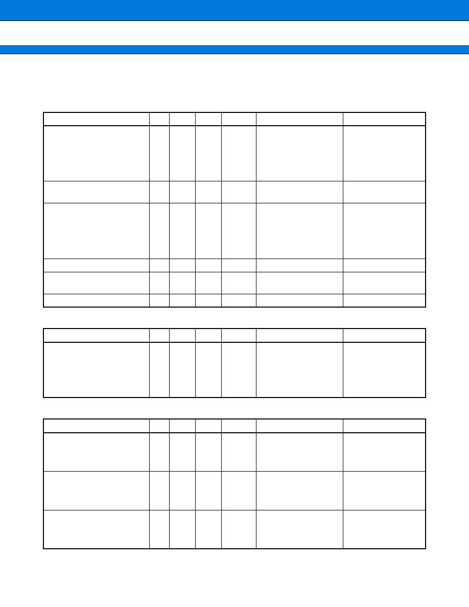
MB91133/MB91F133
108
4.
Detailed Description of Instructions
∑ Add/subtract operation instructions (10 instructions)
∑ Compare operation instructions (3 instructions)
∑ Logical operation instructions (12 instructions)
Mnemonic
Type
OP
Cycle N Z V C
Operation
Remarks
ADD
Rj, Ri
* ADD
#s5, Ri
ADD
#i4, Ri
ADD2
#i4, Ri
A
C'
C
C
A6
A4
A4
A5
1
1
1
1
C C C C
C C C C
C C C C
C C C C
Ri + Rj
Ri
Ri + s5
Ri
Ri + extu (i4)
Ri
Ri + extu (i4)
Ri
MSB is interpreted as
a sign in assembly
language
Zero-extension
Sign-extension
ADDC
Rj, Ri
A
A7
1
C C C C Ri + Rj + c
Ri
Add operation with
sign
ADDN
Rj, Ri
* ADDN
#s5, Ri
ADDN
#i4, Ri
ADDN2
#i4, Ri
A
C'
C
C
A2
A0
A0
A1
1
1
1
1
≠ ≠ ≠ ≠
≠ ≠ ≠ ≠
≠ ≠ ≠ ≠
≠ ≠ ≠ ≠
Ri + Rj
Ri
Ri + s5
Ri
Ri + extu (i4)
Ri
Ri + extu (i4)
Ri
MSB is interpreted as
a sign in assembly
language
Zero-extension
Sign-extension
SUB
Rj, Ri
A
AC
1
C C C C Ri ≠ Rj
Ri
SUBC
Rj, Ri
A
AD
1
C C C C Ri ≠ Rj ≠ c
Ri
Subtract operation with
carry
SUBN
Rj, Ri
A
AE
1
≠ ≠ ≠ ≠ Ri ≠ Rj
Ri
Mnemonic
Type
OP
Cycle N Z V C
Operation
Remarks
CMP
Rj, Ri
* CMP
#s5, Ri
CMP
#i4, Ri
CMP2
#i4, Ri
A
C'
C
C
AA
A8
A8
A9
1
1
1
1
C C C C
C C C C
C C C C
C C C C
Ri ≠ Rj
Ri ≠ s5
Ri + extu (i4)
Ri + extu (i4)
MSB is interpreted as
a sign in assembly
language
Zero-extension
Sign-extension
Mnemonic
Type
OP
Cycle N Z V C
Operation
Remarks
AND
Rj, Ri
AND
Rj, @Ri
ANDH
Rj, @Ri
ANDB
Rj, @Ri
A
A
A
A
82
84
85
86
1
1 + 2a
1 + 2a
1 + 2a
C C ≠ ≠
C C ≠ ≠
C C ≠ ≠
C C ≠ ≠
Ri & = Rj
(Ri) & = Rj
(Ri) & = Rj
(Ri) & = Rj
Word
Word
Half word
Byte
OR
Rj, Ri
OR
Rj, @Ri
ORH
Rj, @Ri
ORB
Rj, @Ri
A
A
A
A
92
94
95
96
1
1 + 2a
1 + 2a
1 + 2a
C C ≠ ≠
C C ≠ ≠
C C ≠ ≠
C C ≠ ≠
Ri | = Rj
(Ri) | = Rj
(Ri) | = Rj
(Ri) | = Rj
Word
Word
Half word
Byte
EOR
Rj, Ri
EOR
Rj, @Ri
EORH
Rj, @Ri
EORB
Rj, @Ri
A
A
A
A
9A
9C
9D
9E
1
1 + 2a
1 + 2a
1 + 2a
C C ≠ ≠
C C ≠ ≠
C C ≠ ≠
C C ≠ ≠
Ri ^ = Rj
(Ri) ^ = Rj
(Ri) ^ = Rj
(Ri) ^ = Rj
Word
Word
Half word
Byte
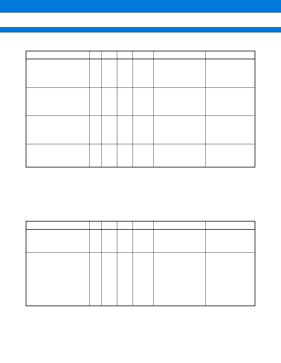
MB91133/MB91F133
109
∑ Bit manipulation arithmetic instructions (8 instructions)
*1: Assembler generates BANDL if result of logical operation "u8&0x0F" leaves an active (set) bit and generates
BANDH if "u8&0xF0" leaves an active bit. Depending on the value in the "u8" format, both BANDL and BANDH
may be generated.
*2: Assembler generates BORL if result of logical operation "u8&0x0F" leaves an active (set) bit and generates
BORH if "u8&0xF0" leaves an active bit.
*3: Assembler generates BEORL if result of logical operation "u8&0x0F" leaves an active (set) bit and generates
BEORH if "u8&0xF0" leaves an active bit.
∑ Add/subtract operation instructions (10 instructions)
*1: DIVOS, DIV1
◊
32, DIV2, DIV3 and DIV4S are generated. A total instruction code length of 72 bytes.
*2: DIVOU and DIV1
◊
32 are generated. A total instruction code length of 66 bytes.
Mnemonic
Type
OP
Cycle N Z V C
Operation
Remarks
BANDL
#u4, @Ri
(u4: 0 to 0F
H
)
BANDH
#u4, @Ri
(u4: 0 to 0F
H
)
* BAND
#u8, @Ri
*
1
C
C
80
81
1 + 2a
1 + 2a
≠
≠ ≠ ≠ ≠
≠ ≠ ≠ ≠
≠ ≠ ≠ ≠
(Ri) & = (F0
H
+ u4)
(Ri) & = ((u4<<4) + 0F
H
)
(Ri) & = u8
Manipulate lower 4 bits
Manipulate upper 4 bits
BORL
#u4, @Ri
(u4: 0 to 0F
H
)
BORH
#u4, @Ri
(u4: 0 to 0F
H
)
* BOR
#u8, @Ri
*
2
C
C
90
91
1 + 2a
1 + 2a
≠
≠ ≠ ≠ ≠
≠ ≠ ≠ ≠
≠ ≠ ≠ ≠
(Ri) | = u4
(Ri) | = (u4<<4)
(Ri) | = u8
Manipulate lower 4 bits
Manipulate upper 4 bits
BEORL
#u4, @Ri
(u4: 0 to 0F
H
)
BEORH
#u4, @Ri
(u4: 0 to 0F
H
)
* BEOR
#u8, @Ri
*
3
C
C
98
99
1 + 2a
1 + 2a
≠
≠ ≠ ≠ ≠
≠ ≠ ≠ ≠
≠ ≠ ≠ ≠
(Ri) ^ = u4
(Ri) ^ = (u4<<4)
(Ri) ^ = u8
Manipulate lower 4 bits
Manipulate upper 4 bits
BTSTL
#u4, @Ri
(u4: 0 to 0F
H
)
BTSTH
#u4, @Ri
(u4: 0 to 0F
H
)
C
C
88
89
2 + a
2 + a
0 C ≠ ≠
C C ≠ ≠
(Ri) & u4
(Ri) & (u4<<4)
Test lower 4 bits
Test upper 4 bits
Mnemonic
Type
OP
Cycle N Z V C
Operation
Remarks
MUL
Rj, Ri
MULU
Rj, Ri
MULH
Rj, Ri
MULUH
Rj, Ri
A
A
A
A
AF
AB
BF
BB
5
5
3
3
C C C ≠
C C C ≠
C C ≠ ≠
C C ≠ ≠
Rj
◊
Ri
MDH, MDL
Rj
◊
Ri
MDH, MDL
Rj
◊
Ri
MDL
Rj
◊
Ri
MDL
32-bit
◊
32-bit = 64-bit
Unsigned
16-bit
◊
16-bit = 32-bit
Unsigned
DIVOS
Ri
DIVOU
Ri
DIV1
Ri
DIV2
Ri
DIV3
DIV4S
* DIV
Ri
*
1
* DIVU
Ri
*
2
E
E
E
E
E
E
97 ≠ 4
97 ≠ 5
97 ≠ 6
97 ≠ 7
9F ≠ 6
9F ≠ 7
1
1
d
1
1
1
≠
≠
≠ ≠ ≠ ≠
≠ ≠ ≠ ≠
≠ C ≠ C
≠ C ≠ C
≠ ≠ ≠ ≠
≠ ≠ ≠ ≠
≠ C ≠ C
≠ C ≠ C
MDL/Ri
MDL,
MDL%Ri
MDH
MDL/Ri
MDL,
MDL%Ri
MDH
Step calculation
32-bit/32-bit = 32-bit
Unsigned
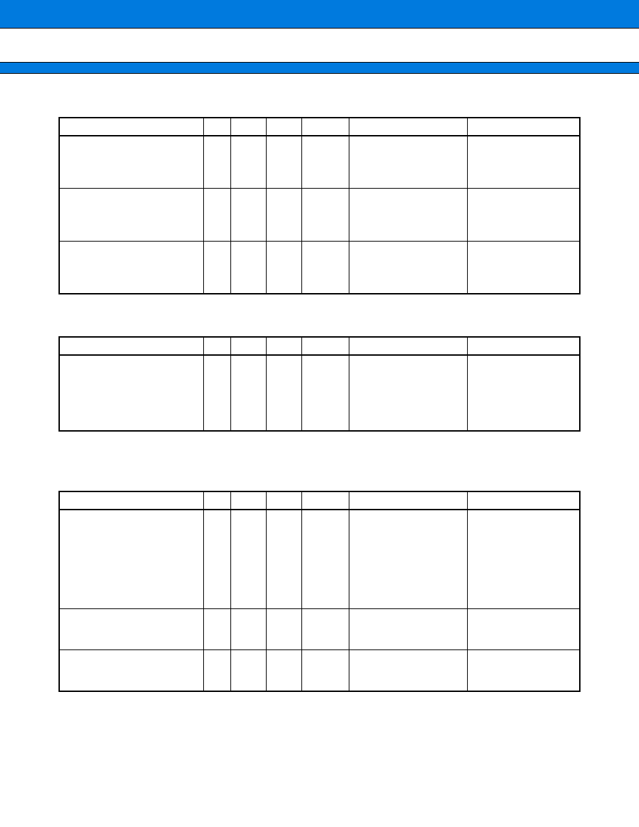
MB91133/MB91F133
110
∑ Shift arithmetic instructions (9 instructions)
∑ Immediate value data transfer instruction (immediate value set/16-bit/32-bit immediate value transfer
instruction) (3 instructions)
*1: If an immediate value is given in absolute, assembler automatically makes i8, i20 or i32 selection.
If an immediate value contains relative value or external reference, assembler selects i32.
∑ Memory load instructions (13 instructions)
Note: The relations between o8 field of TYPE-B and u4 field of TYPE-C in the instruction format and assembler
description from disp8 to disp10 are as follows:
disp8
o8 = disp8:Each disp is a code extension.
disp9
o8 = disp9>>1:Each disp is a code extension.
disp10
o8 = disp10>>2:Each disp is a code extension.
udisp6
u4 = udisp6>>2:udisp4 is a 0 extension.
Mnemonic
Type
OP
Cycle N Z V C
Operation
Remarks
LSL
Rj, Ri
* LSL
#u5, Ri
LSL
#u4, Ri
LSL2
#u4, Ri
A
C'
C
C
B6
B4
B4
B5
1
1
1
1
C C ≠ C
C C ≠ C
C C ≠ C
C C ≠ C
Ri<<Rj
Ri
Ri<<u5
Ri
Ri<<u4
Ri
Ri<<(u4 + 16)
Ri
Logical shift
LSR
Rj, Ri
* LSR
#u5, Ri
LSR
#u4, Ri
LSR2
#u4, Ri
A
C'
C
C
B2
B0
B0
B1
1
1
1
1
C C ≠ C
C C ≠ C
C C ≠ C
C C ≠ C
Ri>>Rj
Ri
Ri>>u5
Ri
Ri>>u4
Ri
Ri>>(u4 + 16)
Ri
Logical shift
ASR
Rj, Ri
* ASR
#u5, Ri
ASR
#u4, Ri
ASR2
#u4, Ri
A
C'
C
C
BA
B8
B8
B9
1
1
1
1
C C ≠ C
C C ≠ C
C C ≠ C
C C ≠ C
Ri>>Rj
Ri
Ri>>u5
Ri
Ri>>u4
Ri
Ri>>(u4 + 16)
Ri
Logical shift
Mnemonic
Type
OP
Cycle N Z V C
Operation
Remarks
LDI: 32
#i32, Ri
LDI: 20
#i20, Ri
LDI: 8
#i8, Ri
* LDI
# {i8 | i20 | i32}, Ri
*
1
E
C
B
9F ≠ 8
9B
C0
3
2
1
≠ ≠ ≠ ≠
≠ ≠ ≠ ≠
≠ ≠ ≠ ≠
i32
Ri
i20
Ri
i8
Ri
{i8 | i20 | i32}
Ri
Upper 12 bits are zero-
extended
Upper 24 bits are zero-
extended
Mnemonic
Type
OP
Cycle N Z V C
Operation
Remarks
LD
@Rj, Ri
LD
@(R13, Rj), Ri
LD
@(R14, disp10), Ri
LD
@(R15, udisp6), Ri
LD
@R15 +, Ri
LD
@R15 +, Rs
LD
@R15 +, PS
A
A
B
C
E
E
E
04
00
20
03
07 ≠ 0
07 ≠ 8
07 ≠ 9
b
b
b
b
b
b
1 + a + b
≠ ≠ ≠ ≠
≠ ≠ ≠ ≠
≠ ≠ ≠ ≠
≠ ≠ ≠ ≠
≠ ≠ ≠ ≠
≠ ≠ ≠ ≠
C C C C
(Rj)
Ri
(R13 + Rj)
Ri
(R14 + disp10)
Ri
(R15 + udisp6)
Ri
(R15)
Ri, R15 + = 4
(R15)
Rs, R15 + = 4
(R15)
PS, R15 + = 4
Rs: Special-purpose
register
LDUH
@Rj, Ri
LDUH
@(R13, Rj), Ri
LDUH
@(R14, disp9), Ri
A
A
B
05
01
40
b
b
b
≠ ≠ ≠ ≠
≠ ≠ ≠ ≠
≠ ≠ ≠ ≠
(Rj)
Ri
(R13 + Rj)
Ri
(R14 + disp9)
Ri
Zero-extension
Zero-extension
Zero-extension
LDUB
@Rj, Ri
LDUB
@(R13, Rj), Ri
LDUB
@(R14, disp8), Ri
A
A
B
06
02
60
b
b
b
≠ ≠ ≠ ≠
≠ ≠ ≠ ≠
≠ ≠ ≠ ≠
(Rj)
Ri
(R13 + Rj)
Ri
(R14 + disp8)
Ri
Zero-extension
Zero-extension
Zero-extension
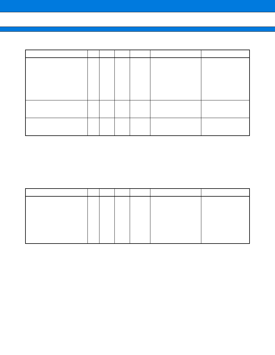
MB91133/MB91F133
111
∑ Memory store instructions (13 instructions)
Note: The relations between o8 field of TYPE-B and u4 field of TYPE-C in the instruction format and assembler
description from disp8 to disp10 are as follows:
disp8
o8 = disp8:Each disp is a code extension.
disp9
o8 = disp9>>1:Each disp is a code extension.
disp10
o8 = disp10>>2:Each disp is a code extension.
udisp6
u4 = udisp6>>2:udisp4 is a 0 extension.
∑ Transfer instructions between registers/special-purpose registers transfer instructions
(5 instructions)
Mnemonic
Type
OP
Cycle N Z V C
Operation
Remarks
ST
Ri, @Rj
ST
Ri, @(R13, Rj)
ST
Ri, @(R14, disp10)
ST
Ri, @(R15, udisp6)
ST
Ri, @≠R15
ST
Rs, @≠R15
ST
PS, @≠R15
A
A
B
C
E
E
E
14
10
30
13
17 ≠ 0
17 ≠ 8
17 ≠ 9
a
a
a
a
a
a
a
≠ ≠ ≠ ≠
≠ ≠ ≠ ≠
≠ ≠ ≠ ≠
≠ ≠ ≠ ≠
≠ ≠ ≠ ≠
≠ ≠ ≠ ≠
≠ ≠ ≠ ≠
Ri
(Rj)
Ri
(R13 + Rj)
Ri
(R14 + disp10)
Ri
(R15 + usidp6)
R15 ≠ = 4, Ri
(R15)
R15 ≠ = 4, Rs
(R15)
R15 ≠ = 4, PS
(R15)
Word
Word
Word
Rs: Special-purpose
register
STH
Ri, @Rj
STH
Ri, @(R13, Rj)
STH
Ri, @(R14, disp9)
A
A
B
15
11
50
a
a
a
≠ ≠ ≠ ≠
≠ ≠ ≠ ≠
≠ ≠ ≠ ≠
Ri
(Rj)
Ri
(R13 + Rj)
Ri
(R14 + disp9)
Half word
Half word
Half word
STB
Ri, @Rj
STB
Ri, @(R13, Rj)
STB
Ri, @(R14, disp8)
A
A
B
16
12
70
a
a
a
≠ ≠ ≠ ≠
≠ ≠ ≠ ≠
≠ ≠ ≠ ≠
Ri
(Rj)
Ri
(R13 + Rj)
Ri
(R14 + disp8)
Byte
Byte
Byte
Mnemonic
Type
OP
Cycle N Z V C
Operation
Remarks
MOV
Rj, Ri
MOV
Rs, Ri
MOV
Ri, Rs
MOV
PS, Ri
MOV
Ri, PS
A
A
A
E
E
8B
B7
B3
17 ≠ 1
07 ≠ 1
1
1
1
1
c
≠ ≠ ≠ ≠
≠ ≠ ≠ ≠
≠ ≠ ≠ ≠
≠ ≠ ≠ ≠
C C C C
Rj
Ri
Rs
Ri
Ri
Rs
PS
Ri
Ri
PS
Transfer between
general-purpose
registers
Rs: Special-purpose
register
Rs: Special-purpose
register
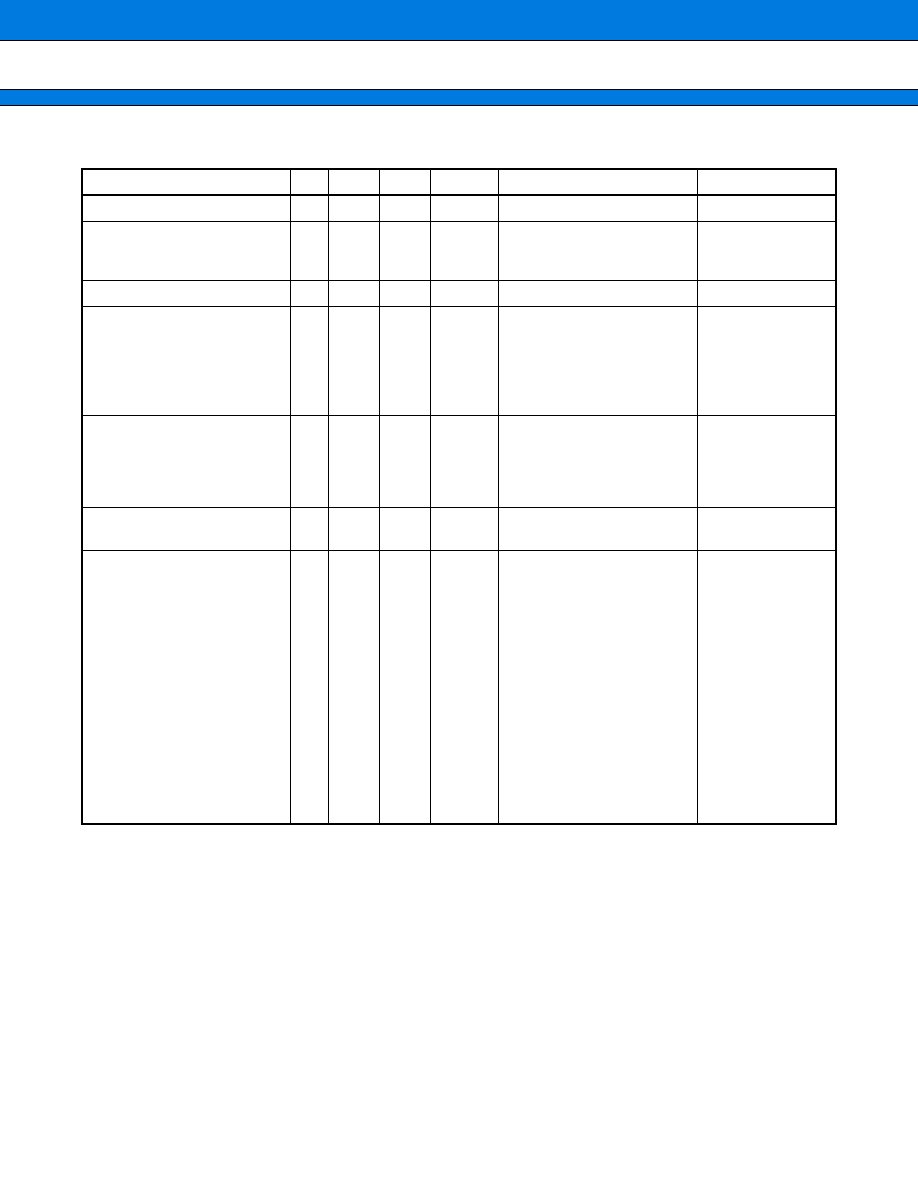
MB91133/MB91F133
112
∑ Non-delay normal branch instructions (23 instructions)
Notes: ∑ "2/1" in cycle sections indicates that 2 cycles are needed for branch and 1 cycle needed for non-branch.
∑ The relations between rel8 field of TYPE-D and rel11 field of TYPE-F in the instruction format and
assembler discription label9 and label12 are as follows.
label9
rel8 = (label9 ≠ PC ≠ 2)/2
label12
rel11 = (label12 ≠ PC ≠ 2)/2
∑ RETI must be operated while S flag = 0.
Mnemonic
Type
OP
Cycle N Z V C
Operation
Remarks
JMP
@Ri
E
97 ≠ 0
2
≠ ≠ ≠ ≠ Ri
PC
CALL
label12
CALL
@Ri
F
E
D0
97 ≠ 1
2
2
≠ ≠ ≠ ≠
≠ ≠ ≠ ≠
PC + 2
RP,
PC + 2 + rel11
◊
2
PC
PC + 2
RP, Ri
PC
RET
E
97 ≠ 2
2
≠ ≠ ≠ ≠ RP
PC
Return
INT
#u8
D
1F
3+3a
≠ ≠ ≠ ≠ SSP ≠ = 4, PS
(SSP),
SSP ≠ = 4,
PC + 2
(SSP),
0
I flag,
0
S flag,
(TBR + 3FC ≠ u8
◊
4)
PC
INTE
E
9F ≠ 3 3 + 3a ≠ ≠ ≠ ≠ SSP ≠ = 4, PS
(SSP),
SSP ≠ = 4,
PC + 2
(SSP),
0
S flag,
(TBR + 3D8 ≠ u8
◊
4)
PC
For emulator
RETI
E
97 ≠ 3 2 + 2a C C C C (R15)
PC, R15 ≠ = 4,
(R15)
PS, R15 ≠ = 4
BNO
label9
BRA
label9
BEQ
label9
BNE
label9
BC
label9
BNC
label9
BN
label9
BP
label9
BV
label9
BNV
label9
BLT
label9
BGE
label9
BLE
label9
BGT
label9
BLS
label9
BHI
label9
D
D
D
D
D
D
D
D
D
D
D
D
D
D
D
D
E1
E0
E2
E3
E4
E5
E6
E7
E8
E9
EA
EB
EC
ED
EE
EF
1
2
2/1
2/1
2/1
2/1
2/1
2/1
2/1
2/1
2/1
2/1
2/1
2/1
2/1
2/1
≠ ≠ ≠ ≠
≠ ≠ ≠ ≠
≠ ≠ ≠ ≠
≠ ≠ ≠ ≠
≠ ≠ ≠ ≠
≠ ≠ ≠ ≠
≠ ≠ ≠ ≠
≠ ≠ ≠ ≠
≠ ≠ ≠ ≠
≠ ≠ ≠ ≠
≠ ≠ ≠ ≠
≠ ≠ ≠ ≠
≠ ≠ ≠ ≠
≠ ≠ ≠ ≠
≠ ≠ ≠ ≠
≠ ≠ ≠ ≠
Non-branch
PC + 2 + rel8
◊
2
PC
PCif Z = = 1
PCif Z = = 0
PCif C = = 1
PCif C = = 0
PCif N = = 1
PCif N = = 0
PCif V = = 1
PCif V = = 0
PCif V xor N = = 1
PCif V xor N = = 0
PCif (V xor N) or Z = = 1
PCif (V xor N) or Z = = 0
PCif C or Z = = 1
PCif C or Z = = 0
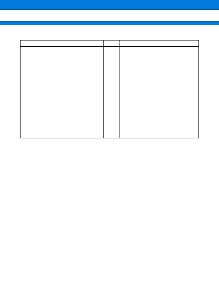
MB91133/MB91F133
113
∑ Branch instructions with delays (20 instructions)
Notes: ∑ The relations between rel8 field of TYPE-D and rel11 field of TYPE-F in the instruction format and
assembler discription label9 and label12 are as follows.
label9
rel8 = (label9 ≠ PC ≠ 2)/2
label12
rel11 = (label12 ≠ PC ≠ 2)/2
∑ Delayed branch operation always executes next instruction (delay slot) before making a branch.
∑ Instructions allowed to be stored in the delay slot must meet one of the following conditions. If the other
instruction is stored, this device may operate other operation than defined.
The instruction described "1" in the other cycle column than branch instruction.
The instruction described "a", "b", "c" or "d" in the cycle column.
Mnemonic
Type
OP
Cycle N Z V C
Operation
Remarks
JMP:D
@Ri
E
9F ≠ 0
1
≠ ≠ ≠ ≠ Ri
PC
CALL:D
label12
CALL:D
@Ri
F
E
D8
9F ≠ 1
1
1
≠ ≠ ≠ ≠
≠ ≠ ≠ ≠
PC + 4
RP,
PC + 2 + rel11
◊
2
PC
PC + 4
RP, Ri
PC
RET:D
E
9F ≠ 2
1
≠ ≠ ≠ ≠ RP
PC
Return
BNO:D
label9
BRA:D
label9
BEQ:D
label9
BNE:D
label9
BC:D
label9
BNC:D
label9
BN:D
label9
BP:D
label9
BV:D
label9
BNV:D
label9
BLT:D
label9
BGE:D
label9
BLE:D
label9
BGT:D
label9
BLS:D
label9
BHI:D
label9
D
D
D
D
D
D
D
D
D
D
D
D
D
D
D
D
F1
F0
F2
F3
F4
F5
F6
F7
F8
F9
FA
FB
FC
FD
FE
FF
1
1
1
1
1
1
1
1
1
1
1
1
1
1
1
1
≠ ≠ ≠ ≠
≠ ≠ ≠ ≠
≠ ≠ ≠ ≠
≠ ≠ ≠ ≠
≠ ≠ ≠ ≠
≠ ≠ ≠ ≠
≠ ≠ ≠ ≠
≠ ≠ ≠ ≠
≠ ≠ ≠ ≠
≠ ≠ ≠ ≠
≠ ≠ ≠ ≠
≠ ≠ ≠ ≠
≠ ≠ ≠ ≠
≠ ≠ ≠ ≠
≠ ≠ ≠ ≠
≠ ≠ ≠ ≠
Non-branch
PC + 2 + rel8
◊
2
PC
PCif Z = = 1
PCif Z = = 0
PCif C = = 1
PCif C = = 0
PCif N = = 1
PCif N = = 0
PCif V = = 1
PCif V = = 0
PCif V xor N = = 1
PCif V xor N = = 0
PCif (V xor N) or Z = = 1
PCif (V xor N) or Z = = 0
PCif C or Z = = 1
PCif C or Z = = 0
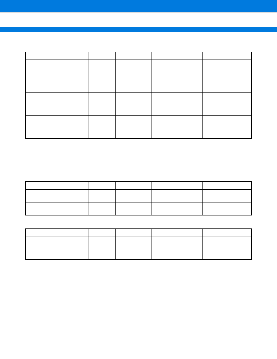
MB91133/MB91F133
114
∑ Direct addressing instructions
Note: The relations between the dir field of TYPE-D in the instruction format and the assembler description from
disp8 to disp10 are as follows:
disp8
dir + disp8:Each disp is a code extension
disp9
dir = disp9>>1:Each disp is a code extension
disp10
dir = disp10>>2:Each disp is a code extension
∑ Resource instructions (2 instructions)
∑ Co-processor instructions (4 instructions)
Mnemonic
Type
OP
Cycle N Z V C
Operation
Remarks
DMOV
@dir10, R13
DMOV
R13, @dir10
DMOV
@dir10, @R13+
DMOV
@R13+, @dir10
DMOV
@dir10, @≠R15
DMOV
@R15+, @dir10
D
D
D
D
D
D
08
18
0C
1C
0B
1B
b
a
2a
2a
2a
2a
≠ ≠ ≠ ≠
≠ ≠ ≠ ≠
≠ ≠ ≠ ≠
≠ ≠ ≠ ≠
≠ ≠ ≠ ≠
≠ ≠ ≠ ≠
(dir10)
R13
R13
(dir10)
(dir10)
(R13), R13 + = 4
(R13)
(dir10), R13 + = 4
R15 ≠ = 4, (dir10)
(R15)
(R15)
(dir10), R15 + = 4
Word
Word
Word
Word
Word
Word
DMOVH
@dir9,
R13
DMOVH
R13, @dir9
DMOVH
@dir9,
@R13+
DMOVH
@R13+, @dir9
D
D
D
D
09
19
0D
1D
b
a
2a
2a
≠ ≠ ≠ ≠
≠ ≠ ≠ ≠
≠ ≠ ≠ ≠
≠ ≠ ≠ ≠
(dir9)
R13
R13
(dir9)
(dir9)
(R13), R13 + = 2
(R13)
(dir9), R13 + = 2
Half word
Half word
Half word
Half word
DMOVB
@dir8,
R13
DMOVB
R13, @dir8
DMOVB
@dir8,
@R13+
DMOVB
@R13+, @dir8
D
D
D
D
0A
1A
0E
1E
b
a
2a
2a
≠ ≠ ≠ ≠
≠ ≠ ≠ ≠
≠ ≠ ≠ ≠
≠ ≠ ≠ ≠
(dir8)
R13
R13
(dir8)
(dir8)
(R13), R13 + +
(R13)
(dir8), R13 + +
Byte
Byte
Byte
Byte
Mnemonic
Type
OP
Cycle N Z V C
Operation
Remarks
LDRES
@Ri+,
#u4
C
BC
a
≠ ≠ ≠ ≠ (Ri)
u4 resource
Ri + = 4
u4: Channel number
STRES
#u4, @Ri+
C
BD
a
≠ ≠ ≠ ≠ u4
resource
(Ri)
Ri + = 4
u4: Channel number
Mnemonic
Type
OP
Cycle N Z V C
Operation
Remarks
COPOP
#u4, #CC, CRj, CRi
COPLD
#u4, #CC, Rj,
CRi
COPST
#u4, #CC, CRj, Ri
COPSV
#u4, #CC, CRj, Ri
E
E
E
E
9F ≠ C
9F ≠ D
9F ≠ E
9F ≠ F
2 + a
1 + 2a
1 + 2a
1 + 2a
≠ ≠ ≠ ≠
≠ ≠ ≠ ≠
≠ ≠ ≠ ≠
≠ ≠ ≠ ≠
Calculation
Rj
CRi
CRj
Ri
CRj
Ri
No error traps
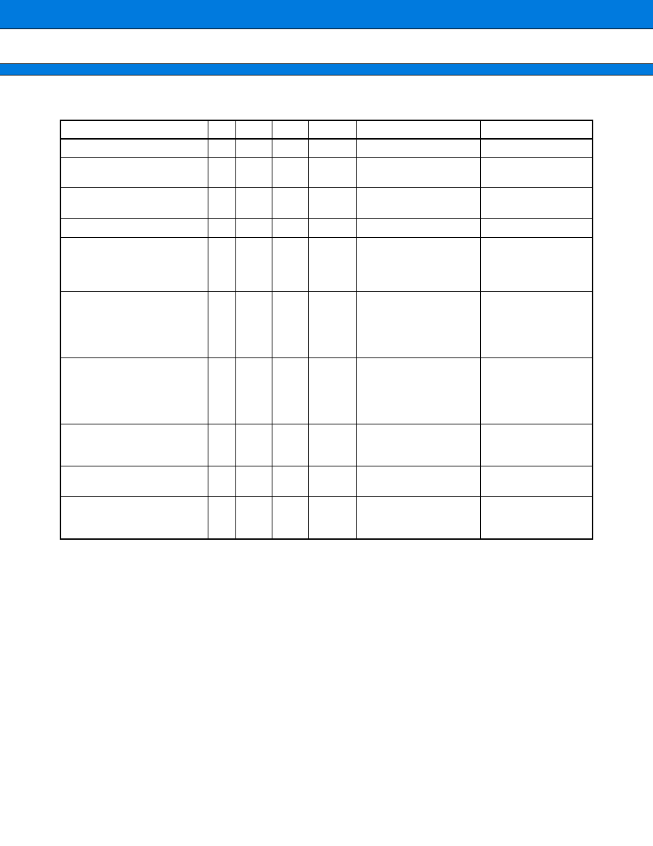
MB91133/MB91F133
115
∑ Other instructions (16 instructions)
*1: In the ADDSP instruction, the reference between u8 of TYPE-D in the instruction format and assembler
description s10 is as follows.
s10
s8 = s10>>2
*2: In the ENTER instruction, the reference between i8 of TYPE-C in the instruction format and assembler
description u10 is as follows.
u10
u8 = u10>>2
*3: If either of R0 to R7 is specified in reglist, assembler generates LDM0. If either of R8 to R15 is specified,
assembler generates LDM1. Both LDM0 and LDM1 may be generated.
*4: The number of cycles needed for execution of LDM0 (reglist) and LDM1 (reglist) is given by the following
calculation; a
◊
(n ≠ 1) + b + 1 when "n" is number of registers specified.
*5: If either of R0 to R7 is specified in reglist, assembler generates STM0. If either of R8 to R15 is specified,
assembler generates STM1. Both STM0 and STM1 may be generated.
*6: The number of cycles needed for execution of STM0 (reglist) and STM1 (reglist) is given by the following
calculation; a
◊
n + 1 when "n" is number of registers specified.
Mnemonic
Type
OP
Cycle N Z V C
Operation
Remarks
NOP
E
9F ≠ A
1
≠ ≠ ≠ ≠ No changes
ANDCCR #u8
ORCCR
#u8
D
D
83
93
c
c
C C C C
C C C C
CCR and u8
CCR
CCR or u8
CCR
STILM
#u8
D
87
1
≠ ≠ ≠ ≠ i8
ILM
Set ILM immediate
value
ADDSP
#s10
*
1
D
A3
1
≠ ≠ ≠ ≠ R15 + = s10
ADD SP instruction
EXTSB
Ri
EXTUB
Ri
EXTSH
Ri
EXTUH
Ri
E
E
E
E
97 ≠ 8
97 ≠ 9
97 ≠ A
97 ≠ B
1
1
1
1
≠ ≠ ≠ ≠
≠ ≠ ≠ ≠
≠ ≠ ≠ ≠
≠ ≠ ≠ ≠
Sign extension 8
32 bits
Zero extension 8
32 bits
Sign extension 16
32 bits
Zero extension 16
32 bits
LDM0
(reglist)
LDM1
(reglist)
* LDM
(reglist)
*
3
D
D
8C
8D
*
4
*
4
≠
≠ ≠ ≠ ≠
≠ ≠ ≠ ≠
≠ ≠ ≠ ≠
(R15)
reglist,
R15 increment
(R15)
reglist,
R15 increment
(R15 + +)
reglist,
Load-multi R0 to R7
Load-multi R8 to R15
Load-multi R0 to R15
STM0
(reglist)
STM1
(reglist)
* STM2
(reglist)
*
5
D
D
8E
8F
*
6
*
6
≠
≠ ≠ ≠ ≠
≠ ≠ ≠ ≠
≠ ≠ ≠ ≠
R15 decrement,
reglist
(R15)
R15 decrement,
reglist
(R15)
reglist
(R15 + +)
Store-multi R0 to R7
Store-multi R8 to R15
Store-multi R0 to R15
ENTER
#u10
*
2
D
0F
1+a
≠ ≠ ≠ ≠ R14
(R15 ≠ 4),
R15 ≠ 4
R14,
R15 ≠ u10
R15
Entrance processing
of function
LEAVE
E
9F ≠ 9
b
≠ ≠ ≠ ≠ R14 + 4
R15,
(R15 ≠ 4)
R14
Exit processing of
function
XCHB
@Rj, Ri
A
8A
2a
≠ ≠ ≠ ≠ Ri
TEMP,
(Rj)
Ri,
TEMP
(Rj)
For SEMAFO
management
Byte data

MB91133/MB91F133
116
∑ 20-bit normal branch macro instructions
*1: CALL20
(1) If label20 ≠ PC ≠ 2 is between ≠0x800 and +0x7fe, instruction is generated as follows;
CALL
label12
(2) If label20 ≠ PC ≠ 2 is outside of the range given in (1) or includes external reference symbol, instruction is
generated as follows;
LDI:20
#label20, Ri
CALL
@Ri
*2: BRA20
(1) If label20 ≠ PC ≠ 2 is between ≠0x100 and +0xfe, instruction is generated as follows;
BRA
label9
(2) If label20 ≠ PC ≠ 2 is outside of the range given in (1) or includes external reference symbol, instruction is
generated as follows;
LDI:20
#label20, Ri
JMP
@Ri
*3: Bcc20 (BEQ20 to BHI20)
(1) If label20 ≠ PC ≠ 2 is between ≠0x100 and +0xfe, instruction is generated as follows;
Bcc
label9
(2) If label20 ≠ PC ≠ 2 is outside of the range given in (1) or includes external reference symbol, instruction is
generated as follows;
Bxcc
false
xcc is a revolt condition of cc
LDI:20
#label20, Ri
JMP
@Ri
false:
Mnemonic
Operation
Remarks
* CALL20
label20, Ri
Next instruction address
RP, label20
PC
Ri: Temporary register
*
1
* BRA20
label20, Ri
* BEQ20
label20, Ri
* BNE20
label20, Ri
* BC20
label20, Ri
* BNC20
label20, Ri
* BN20
label20, Ri
* BP20
label20, Ri
* BV20
label20, Ri
* BNV20
label20, Ri
* BLT20
label20, Ri
* BGE20
label20, Ri
* BLE20
label20, Ri
* BGT20
label20, Ri
* BLS20
label20, Ri
* BHI20
label20, Ri
label20
PC
if (Z = = 1) then label20
PC
ifs/Z = = 0
ifs/C = = 1
ifs/C = = 0
ifs/N = = 1
ifs/N = = 0
ifs/V = = 1
ifs/V = = 0
ifs/V xor N = = 1
ifs/V xor N = = 0
ifs/(V xor N) or Z = = 1
ifs/(V xor N) or Z = = 0
ifs/C or Z = = 1
ifs/C or Z = = 0
Ri: Temporary register
*
2
Ri: Temporary register
*
3
Ri: Temporary register
*
3
Ri: Temporary register
*
3
Ri: Temporary register
*
3
Ri: Temporary register
*
3
Ri: Temporary register
*
3
Ri: Temporary register
*
3
Ri: Temporary register
*
3
Ri: Temporary register
*
3
Ri: Temporary register
*
3
Ri: Temporary register
*
3
Ri: Temporary register
*
3
Ri: Temporary register
*
3
Ri: Temporary register
*
3

MB91133/MB91F133
117
∑ 20-bit delayed branch macro instructions
*1: CALL20:D
(1) If label20 ≠ PC ≠ 2 is between ≠0x800 and +0x7fe, instruction is generated as follows;
CALL:D label12
(2) If label20 ≠ PC ≠ 2 is outside of the range given in (1) or includes external reference symbol, instruction is
generated as follows;
LDI:20
#label20, Ri
CALL:D @Ri
*2: BRA20:D
(1) If label20 ≠ PC ≠ 2 is between ≠0x100 and +0xfe, instruction is generated as follows;
BRA:D
label9
(2) If label20 ≠ PC ≠ 2 is outside of the range given in (1) or includes external reference symbol, instruction is
generated as follows;
LDI:20
#label20, Ri
JMP:D
@Ri
*3: Bcc20:D (BEQ20:D to BHI20:D)
(1) If label20 ≠ PC ≠ 2 is between ≠0x100 and +0xfe, instruction is generated as follows;
Bcc:D
label9
(2) If label20 ≠ PC ≠ 2 is outside of the range given in (1) or includes external reference symbol, instruction is
generated as follows;
Bxcc
false
xcc is a revolt condition of cc
LDI:20
#label20, Ri
JMP:D
@Ri
false:
Mnemonic
Operation
Remarks
* CALL20:D label20, Ri
Next instruction address + 2
RP, label20
PC
Ri: Temporary register
*
1
* BRA20:D label20, Ri
* BEQ20:D label20, Ri
* BNE20:D label20, Ri
* BC20:D
label20, Ri
* BNC20:D label20, Ri
* BN20:D
label20, Ri
* BP20:D
label20, Ri
* BV20:D
label20, Ri
* BNV20:D label20, Ri
* BLT20:D
label20, Ri
* BGE20:D label20, Ri
* BLE20:D
label20, Ri
* BGT20:D label20, Ri
* BLS20:D
label20, Ri
* BHI20:D
label20, Ri
label20
PC
if (Z = = 1) then label20
PC
ifs/Z = = 0
ifs/C = = 1
ifs/C = = 0
ifs/N = = 1
ifs/N = = 0
ifs/V = = 1
ifs/V = = 0
ifs/V xor N = = 1
ifs/V xor N = = 0
ifs/(V xor N) or Z = = 1
ifs/(V xor N) or Z = = 0
ifs/C or Z = = 1
ifs/C or Z = = 0
Ri: Temporary register
*
2
Ri: Temporary register
*
3
Ri: Temporary register
*
3
Ri: Temporary register
*
3
Ri: Temporary register
*
3
Ri: Temporary register
*
3
Ri: Temporary register
*
3
Ri: Temporary register
*
3
Ri: Temporary register
*
3
Ri: Temporary register
*
3
Ri: Temporary register
*
3
Ri: Temporary register
*
3
Ri: Temporary register
*
3
Ri: Temporary register
*
3
Ri: Temporary register
*
3

MB91133/MB91F133
118
∑ 32-bit normal macro branch instructions
*1: CALL32
(1) If label32 ≠ PC ≠ 2 is between ≠0x800 and +0x7fe, instruction is generated as follows;
CALL
label12
(2) If label32 ≠ PC ≠ 2 is outside of the range given in (1) or includes external reference symbol, instruction is
generated as follows;
LDI:32
#label32, Ri
CALL
@Ri
*2: BRA32
(1) If label32 ≠ PC ≠ 2 is between ≠0x100 and +0xfe, instruction is generated as follows;
BRA
label9
(2) If label32 ≠ PC ≠ 2 is outside of the range given in (1) or includes external reference symbol, instruction is
generated as follows;
LDI:32
#label32, Ri
JMP
@Ri
*3: Bcc32 (BEQ32 to BHI32)
(1) If label32 ≠ PC ≠ 2 is between ≠0x100 and +0xfe, instruction is generated as follows;
Bcc
label9
(2) If label32 ≠ PC ≠ 2 is outside of the range given in (1) or includes external reference symbol, instruction is
generated as follows;
Bxcc
false
xcc is a revolt condition of cc
LDI:32
#label32, Ri
JMP
@Ri
false:
Mnemonic
Operation
Remarks
* CALL32
label32, Ri
Next instruction address
RP, label32
PC
Ri: Temporary register
*
1
* BRA32
label32, Ri
* BEQ32
label32, Ri
* BNE32
label32, Ri
* BC32
label32, Ri
* BNC32
label32, Ri
* BN32
label32, Ri
* BP32
label32, Ri
* BV32
label32, Ri
* BNV32
label32, Ri
* BLT32
label32, Ri
* BGE32
label32, Ri
* BLE32
label32, Ri
* BGT32
label32, Ri
* BLS32
label32, Ri
* BHI32
label32, Ri
label32
PC
if (Z = = 1) then label32
PC
ifs/Z = = 0
ifs/C = = 1
ifs/C = = 0
ifs/N = = 1
ifs/N = = 0
ifs/V = = 1
ifs/V = = 0
ifs/V xor N = = 1
ifs/V xor N = = 0
ifs/(V xor N) or Z = = 1
ifs/(V xor N) or Z = = 0
ifs/C or Z = = 1
ifs/C or Z = = 0
Ri: Temporary register
*
2
Ri: Temporary register
*
3
Ri: Temporary register
*
3
Ri: Temporary register
*
3
Ri: Temporary register
*
3
Ri: Temporary register
*
3
Ri: Temporary register
*
3
Ri: Temporary register
*
3
Ri: Temporary register
*
3
Ri: Temporary register
*
3
Ri: Temporary register
*
3
Ri: Temporary register
*
3
Ri: Temporary register
*
3
Ri: Temporary register
*
3
Ri: Temporary register
*
3

MB91133/MB91F133
119
∑ 32-bit delayed macro branch instructions
*1: CALL32:D
(1) If label32 ≠ PC ≠ 2 is between ≠0x800 and +0x7fe, instruction is generated as follows;
CALL:D label12
(2) If label32 ≠ PC ≠ 2 is outside of the range given in (1) or includes external reference symbol, instruction is
generated as follows;
LDI:32
#label32, Ri
CALL:D @Ri
*2: BRA32:D
(1) If label32 ≠ PC ≠ 2 is between ≠0x100 and +0xfe, instruction is generated as follows;
BRA:D
label9
(2) If label32 ≠ PC ≠ 2 is outside of the range given in (1) or includes external reference symbol, instruction is
generated as follows;
LDI:32
#label32, Ri
JMP:D
@Ri
*3: Bcc32:D (BEQ32:D to BHI32:D)
(1) If label32 ≠ PC ≠ 2 is between ≠0x100 and +0xfe, instruction is generated as follows;
Bcc:D
label9
(2) If label32 ≠ PC ≠ 2 is outside of the range given in (1) or includes external reference symbol, instruction is
generated as follows;
Bxcc
false
xcc is a revolt condition of cc
LDI:32
#label32, Ri
JMP:D
@Ri
false:
Mnemonic
Operation
Remarks
* CALL32:D label32, Ri
Next instruction address + 2
RP, label32
PC
Ri: Temporary register
*
1
* BRA32:D label32, Ri
* BEQ32:D label32, Ri
* BNE32:D label32, Ri
* BC32:D
label32, Ri
* BNC32:D label32, Ri
* BN32:D
label32, Ri
* BP32:D
label32, Ri
* BV32:D
label32, Ri
* BNV32:D label32, Ri
* BLT32:D
label32, Ri
* BGE32:D label32, Ri
* BLE32:D
label32, Ri
* BGT32:D label32, Ri
* BLS32:D
label32, Ri
* BHI32:D
label32, Ri
label32
PC
if (Z = = 1) then label32
PC
ifs/Z = = 0
ifs/C = = 1
ifs/C = = 0
ifs/N = = 1
ifs/N = = 0
ifs/V = = 1
ifs/V = = 0
ifs/V xor N = = 1
ifs/V xor N = = 0
ifs/(V xor N) or Z = = 1
ifs/(V xor N) or Z = = 0
ifs/C or Z = = 1
ifs/C or Z = = 0
Ri: Temporary register
*
2
Ri: Temporary register
*
3
Ri: Temporary register
*
3
Ri: Temporary register
*
3
Ri: Temporary register
*
3
Ri: Temporary register
*
3
Ri: Temporary register
*
3
Ri: Temporary register
*
3
Ri: Temporary register
*
3
Ri: Temporary register
*
3
Ri: Temporary register
*
3
Ri: Temporary register
*
3
Ri: Temporary register
*
3
Ri: Temporary register
*
3
Ri: Temporary register
*
3
MB91133/MB91F133
120
s
ORDERING INFORMATION
Part number
Package
Remarks
MB91133PMT2-XXX
144-pin plastic LQFP
(FPT-144P-M08)
MB91133PBT-XXX
144-pin plastic FBGA
(BGA-144P-M01)
MB91F133PMT2
144-pin plastic LQFP
(FPT-144P-M08)
MB91F133PBT
144-pin plastic FBGA
(BGA-144P-M01)
MB91FV130CR-ES
299-pin ceramic PGA
(PGA-299)
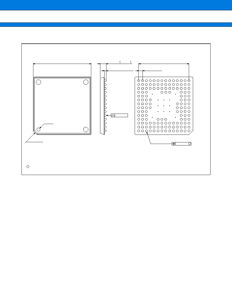
MB91133/MB91F133
121
s
PACKAGE DIMENSIONS
144-pin plastic FBGA
(BGA-144P-M01)
Note) Corner shape may differ from the diagram.
Dimensions in mm (inches)
C
1998 FUJITSU LIMITED B144001S-2C-2
12.00±0.10(.472±.004)SQ
.049
≠.004
+.008
≠0.10
+0.20
1.25
(Mounting height)
0.38±0.10(.015±.004)
(Stand off)
0.10(.004)
C0.80(.031)
INDEX
10.40(.409)REF
0.80(.031)TYP
1
2
3
4
5
6
7
8
9
10
11
L
K
J
H G F E D C B A
144-ÿ0.45±0.10
(144-ÿ.018±.004)
M
0.08(.003)
12
13
M
N
P
14

MB91133/MB91F133
122
144-pin plastic LQFP
(FPT-144P-M08)
Dimensions in mm (inches)
C
1995 FUJITSU LIMITED F144019S-1C-2
Details of "A" part
Details of "B" part
0.50±0.20(.020±.008)
0 10∞
0.40(.016)MAX
0.15(.006)MAX
0.15(.006)
0.15(.006)
22.00±0.30(.866±.012)SQ
20.00±0.10(.787±.004)SQ
0.20±0.10
(.008±.004)
0.08(.003)
M
0.15±0.05
(.006±.002)
1.70(.67)MAX
0(0)MIN
(STAND OFF)
21.00
17.50
(.827)
NOM
(.686)
REF
0.10(.004)
"A"
"B"
36
37
72
73
108
109
144
1
INDEX
0.50(.0197)TYP
LEAD No.

MB91133/MB91F133
FUJITSU LIMITED
For further information please contact:
Japan
FUJITSU LIMITED
Corporate Global Business Support Division
Electronic Devices
Shinjuku Dai-Ichi Seimei Bldg. 7-1,
Nishishinjuku 2-chome, Shinjuku-ku,
Tokyo 163-0721, Japan
Tel: +81-3-5322-3347
Fax: +81-3-5322-3386
http://edevice.fujitsu.com/
North and South America
FUJITSU MICROELECTRONICS, INC.
3545 North First Street,
San Jose, CA 95134-1804, U.S.A.
Tel: +1-408-922-9000
Fax: +1-408-922-9179
Customer Response Center
Mon. - Fri.: 7 am - 5 pm (PST)
Tel: +1-800-866-8608
Fax: +1-408-922-9179
http://www.fujitsumicro.com/
Europe
FUJITSU MICROELECTRONICS EUROPE GmbH
Am Siebenstein 6-10,
D-63303 Dreieich-Buchschlag,
Germany
Tel: +49-6103-690-0
Fax: +49-6103-690-122
http://www.fujitsu-fme.com/
Asia Pacific
FUJITSU MICROELECTRONICS ASIA PTE. LTD.
#05-08, 151 Lorong Chuan,
New Tech Park,
Singapore 556741
Tel: +65-281-0770
Fax: +65-281-0220
http://www.fmap.com.sg/
Korea
FUJITSU MICROELECTRONICS KOREA LTD.
1702 KOSMO TOWER, 1002 Daechi-Dong,
Kangnam-Gu,Seoul 135-280
Korea
Tel: +82-2-3484-7100
Fax: +82-2-3484-7111
F0101
©
FUJITSU LIMITED Printed in Japan
All Rights Reserved.
The contents of this document are subject to change without notice.
Customers are advised to consult with FUJITSU sales
representatives before ordering.
The information and circuit diagrams in this document are
presented as examples of semiconductor device applications, and
are not intended to be incorporated in devices for actual use. Also,
FUJITSU is unable to assume responsibility for infringement of
any patent rights or other rights of third parties arising from the use
of this information or circuit diagrams.
The contents of this document may not be reproduced or copied
without the permission of FUJITSU LIMITED.
FUJITSU semiconductor devices are intended for use in standard
applications (computers, office automation and other office
equipments, industrial, communications, and measurement
equipments, personal or household devices, etc.).
CAUTION:
Customers considering the use of our products in special
applications where failure or abnormal operation may directly
affect human lives or cause physical injury or property damage, or
where extremely high levels of reliability are demanded (such as
aerospace systems, atomic energy controls, sea floor repeaters,
vehicle operating controls, medical devices for life support, etc.)
are requested to consult with FUJITSU sales representatives before
such use. The company will not be responsible for damages arising
from such use without prior approval.
Any semiconductor devices have inherently a certain rate of failure.
You must protect against injury, damage or loss from such failures
by incorporating safety design measures into your facility and
equipment such as redundancy, fire protection, and prevention of
over-current levels and other abnormal operating conditions.
If any products described in this document represent goods or
technologies subject to certain restrictions on export under the
Foreign Exchange and Foreign Trade Control Law of Japan, the
prior authorization by Japanese government should be required for
export of those products from Japan.