DS07-16506-1E
FUJITSU SEMICONDUCTOR
DATA SHEET
32-bit Microcontroller
CMOS
FR60Lite
MB91230 Series
MB91233L/MB91F233/MB91F233L/MB91V230
s
s
s
s
DESCRIPTION
The MB91230 series is a line of standard microcontrollers, based on a 32-bit high-performance RISC CPU and
containing variety of I/O resources, for embedded control applications which require high CPU performance at
high speed processing.
Audio motor control storage : Designed to specifications for embedded control applications which high CPU
performance power processing.
The MB91230 series belongs to the FR60Lite family.
s
s
s
s
FEATURES
∑ 32-bit RISC, load/store architecture with a 5 stage pipeline
∑ Maximum operating frequency: 33.6 MHz (oscillation frequency
=
4.2 MHz, oscillation frequency 8-multiplier
(PLL clock multiplication method) )
∑ 16-bit fixed length instructions (basic instructions)
∑ Execution speed of instructions : 1 instruction per cycle
(Continued)
s
s
s
s
PACKAGES
401-pin Ceramic PGA
120-pin Plastic LQFP
128-pin plastic FLGA
(PGA-401C-A02)
(FPT-120P-M05)
(LGA-128P-M01)

MB91230 Series
2
(Continued)
∑ Memory-to-memory transfer, bit handling, and barrel shift instructions, etc. : Instructions suitable for embedded
applications
∑ Function entry/exit instructions, multiple-register load/store instructions : Instructions adapted for C-language
∑ Register interlock function : Facilitates coding in assembler
∑ Built-in multiplier with instruction-level support
- 32-bit multiplication with sign : 5 cycles
- 16-bit multiplication with sign : 3 cycles
∑ Interrupt (PC and PS save) : 6 cycles (16 priority levels)
∑ Harvard architecture allowing program access and data access to be executed simultaneously
∑ Instruction compatible with FR family
∑ Capacity of built-in ROM and ROM type
- MASK ROM
: 256 KB
- FLASH ROM
: 256 KB
∑ Capacity of built-in RAM : 16 KB
∑ General-purpose ports : Maximum 98 ports (including N-ch open-drain port : 4 ports)
∑ A/D converter (series-parallel type)
- Resolution : 10-bit : 8 ch (4 ch
◊
2 unit)
- Conversion time : 1.69
µ
s (Minimum conversion time)
∑ D/A converter (R-2R type)
- Resolution : 8-bit : 2 ch (independence)
- Conversion speed : 0.6
µ
s (when load capacitance 20 pF)
∑ External interrupt input : 16 ch
∑ Bit search module (for REALOS)
- Function for searching the MSB (Upper bit) in each word for the first "0" or "1" inverted point
∑ UART (full-duplex double buffer) : 4 ch
- Selectable parity On/Off
- Asynchronous (start-stop synchronized) or clock-synchronous communications selectable
- Internal timer for dedicated baud rate (U-timer) on each channel
- External clock can be used as transfer clock
- Error detection function for parity, frame and overrun
∑ PPG : 16-bit
◊
6 ch
∑ Up/down counter : 2 ch (8-bit
◊
2 ch or 16-bit
◊
1 ch)
∑ Reload timer : 16-bit
◊
4 ch
∑ Free-run timer : 16-bit
◊
2 ch
∑ Watch timer : 15-bit
◊
1 ch
∑ PWC : 8-bit
◊
2 ch
∑ Input capture : 2 ch (interface with free-run timer 0)
∑ Output compare : 4 ch (free-run timer 0 and output compare unit 0/1 cooperate, free-run timer 1 and
output compare units 2/3)
∑ LCD controller : SEG00 to SEG31/COM0 to COM3 (also serving as a port)
∑ Clock monitor (peripheral clock output function) : 1 ch
∑ Timebase/watchdog timer (26-bit)
∑ Real-time clock (counting even with the real-time clock stopped)
∑ Low Power Consumption Mode
∑ Sleep/stop function
∑ Package : LQFP-120, FLGA-128
∑ Technology : CMOS 0.35
µ
m
∑ Power supply
∑ Dual power supply configuration [internal logic 3.3 V, I/O 5.5 V(3.3 V for ADC and DAC input/output)]
Note : Do not set the external bus mode in which the MB91230 series cannot operate.
MB91230 Series
3
s
s
s
s
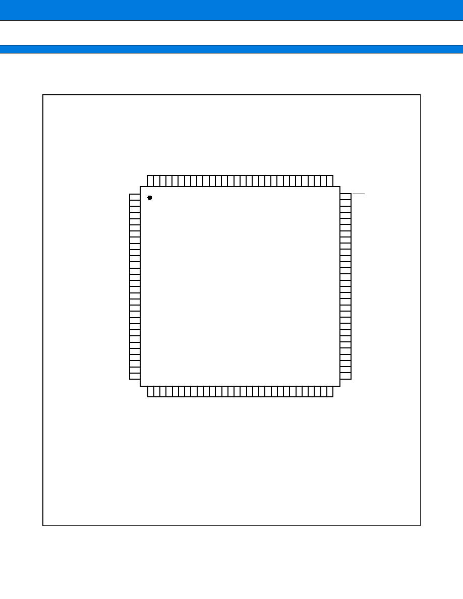
PIN ASSIGNMENT
∑
MB91233L, MB91F233, MB91F233L
(Continued)
1
2
3
4
5
6
7
8
9
10
11
12
13
14
15
16
17
18
19
20
21
22
23
24
25
26
27
28
29
30
P26/SCK2
P27/SIN3
P30/SOT3
P31/SCK3
P32/AIN0
P33/BIN0
P34/ZIN0
P35/AIN1
P36/BIN1
P37/ZIN1
P40/PPG0
P41/PPG1
X0A
X1A
V
CC
3B
V
SS
V
CC
3
P42/PPG2
P43/PPG3
P44/TOT0
P45/TOT1
P46/TOT2
P47/CKOT
P50/INT8
P51/INT9
P52/INT10
P53/INT11/PPG4
P54/INT12/PPG5
P55/INT13/TIN2
P56/INT14/TIN1
90
89
88
87
86
85
84
83
82
81
80
79
78
77
76
75
74
73
72
71
70
69
68
67
66
65
64
63
62
61
INIT
MD0
MD1
MD2
P73/COM3
P72/COM2
P71/COM1
P70/COM0
P67/SEG31
P66/SEG30
P65/SEG29
P64/SEG28
PB3/SEG27
PB2/SEG26
V
SS
V
CC
PB1/SEG25
PB0/SEG24
PA7/SEG23
PA6/SEG22
PA5/SEG21
PA4/SEG20
PA3/SEG19
PA2/SEG18
PA1/SEG17
PA0/SEG16
P97/SEG15
P96/SEG14
P95/SEG13
P94/SEG12
31
32
33
34
35
36
37
38
39
40
41
42
43
44
45
46
47
48
49
50
51
52
53
54
55
56
57
58
59
60
P57/INT15/TIN0/ADTG0
PF3/T
O
T
3
PF4/TIN3/ADTG1
PD0/D
A0
PD1/D
A1
AV
CC
A
VRH
AV
SS
PC0/AN0
PC1/AN1
PC2/AN2
PC3/AN3
PC4/AN4
PC5/AN5
PC6/AN6
PC7/AN7
V
SS
V
CC
3IO
P80/SEG0
P81/SEG1
P82/SEG2
P83/SEG3
P84/SEG4
P85/SEG5
P86/SEG6
P87/SEG7
P90/SEG8
P91/SEG9
P92/SEG10
P93/SEG11
120
119
118
117
116
115
114
113
112
111
110
109
108
107
106
105
104
103
102
101
100
99
98
97
96
95
94
93
92
91
P25/SO
T2
P24/SIN2
P23/PWI1/OP3
P22/PWI0/OP2
P21/CKI1/OP1
P20/CKI0/OP0
P17/INT7
P16/INT6
P15/INT5
P14/INT4
P13/INT3
P12/INT2
X0
X1
V
SS
V
CC
P11/INT1
P10/INT0
P07/IC1
P06/IC0
P05/SCK1
P04/SO
T1
P03/SIN1
P02/SCK0
P01/SO
T0
P00/SIN0
V3
V2
V1
V0
(TOP VIEW)
(FPT-120P-M05)
* : Open-drain
MB91230 Series
4
(Continued)
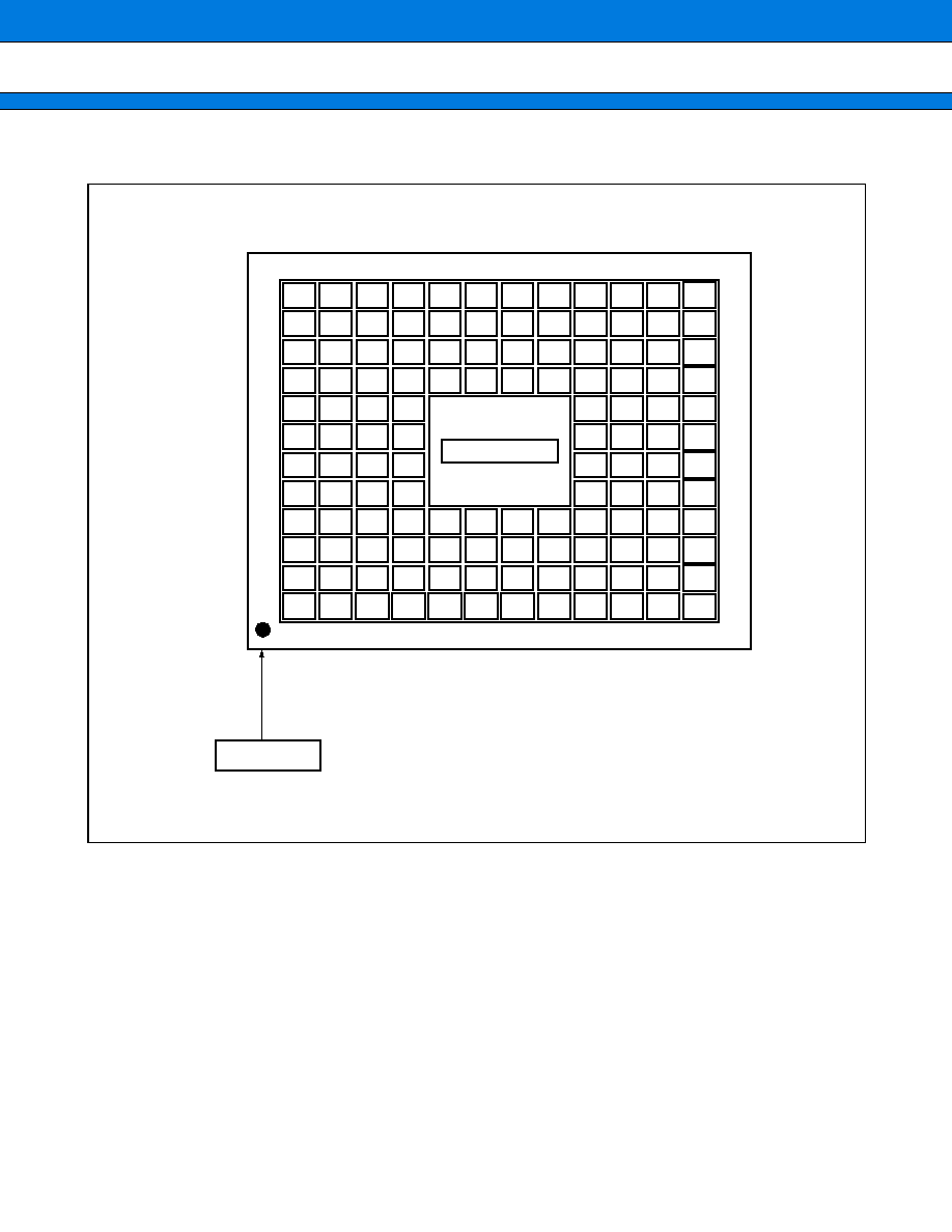
∑
MB91F233L
M1
M2
M3
M4
M5
M6
M7
M8
M9
M10
M11
M12
L1
L2
L3
L4
L5
L6
L7
L8
L9
L10
L11
L12
K1
K2
K3
K4
K5
K6
K7
K8
K9
K10
K11
K12
J1
J2
J3
J4
J5
J6
J7
J8
J9
J10
J11
J12
H1
H2
H3
H4
H9
H10
H11
H12
G1
G2
G3
G4
G9
G10
G11
G12
F1
F2
F3
F4
F9
F10
F11
F12
E1
E2
E3
E4
E9
E10
E11
E12
D1
D2
D3
D4
D5
D6
D7
D8
D9
D10
D11
D12
C1
C2
C3
C4
C5
C6
C7
C8
C9
C10
C11
C12
B1
B2
B3
B4
B5
B6
B7
B8
B9
B10
B11
B12
A1
M
L
K
J
H
G
F
E
D
C
B
A
A2
A3
A4
A5
A6
A7
A8
A9
A10
A11
A12
1
2
3
4
5
6
7
8
9
10
11
12
TOP VIEW
INDEX
(LGA-128P-M01)
MB91230 Series
5
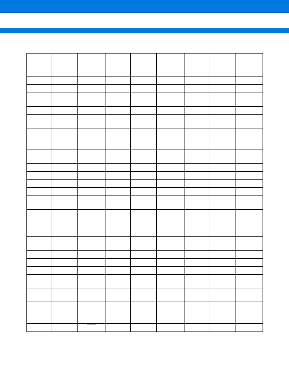
Pin correspondence table of LQFP-120 and FLGA-128 in MB91230 series (LGA-128P-M01)
(Continued)
LQFP-120
No.
FLGA-128
No.
(JEDEC
No.)
Signal
name
LQFP-120
No.
FLGA-128
No.
(JEDEC
No.)
Signal
name
LQFP-120
No.
FLGA-128
No.
(JEDEC
No.
)
Signal
name
1
A1
P26/SCK2
98
C9
P03/SIN1
18
G1
P42/PPG2
120
A2
P25/SOT2
93
C10
V2
15
G2
V
CC
3B
117
A3
P22/PWI0/
OP2
85
C11
P72/COM2
*2
G3*
4
V
CC
3*
4
114
A4
P17/INT7
87
C12
MD2
17
G4
V
CC
3
A5
*5
10
D1
P37/ZIN1
71
G9
PA6/
SEG22
109
A6
P12/INT2
6
D2
P33/BIN0
75
G10
V
CC
107
A7
X1
8
D3
P35/AIN1
74
G11
PB1/
SEG25
103
A8
P10/INT0
119
D4
P24/SIN2
77
G12
PB2/
SEG26
100
A9
P05/SCK1
111
D5
P14/INT4
21
H1
P45/TOT1
97
A10
P02/SCK0
D6
*5
19
H2
P43/PPG3
94
A11
V3
101
D7
P06/IC0
23
H3
P47/CKOT
91
A12
V0
95
D8
P00/SIN0
20
H4
P44/TOT0
4
B1
P31/SCK3
89
D9
MD0
65
H9
PA0/
SEG16
118
B2
P23/PWI1/
OP3
86
D10
P73/COM3
72
H10
PA7/
SEG23
115
B3
P20/CKI0/
OP0
82
D11
P67/
SEG31*
1
69
H11
PA4/
SEG20
112
B4
P15/INT5
84
D12
P71/COM1
73
H12
PB0/
SEG24
110
B5
P13/INT3
13
E1
X0A
24
J1
P50/INT8
106
B6
V
SS
9
E2
P36/BIN1
22
J2
P46/TOT2
104
B7
P11/INT1
12
E3
P41/PPG1
26
J3
P52/INT10
99
B8
P04/SOT1
5
E4
P32/AIN0
29
J4
P55/INT13/
TIN2
96
B9
P01/SOT0
81
E9
P66/
SEG30*
1
35
J5
PD1/DA1
92
B10
V1
83
E10
P70/COM0
40
J6
PC1/AN1
88
B11
MD1
80
E11
P65/
SEG29*
1
47
J7
V
SS
90
B12
INIT
E12
*5
50
J8
P81/SEG1

MB91230 Series
6
(Continued)
*1 : Open-drain
*2 : Connected to pin 17(V
CC
3) on the LQFP120 version
*3 : Connected to pin 38(AV
SS
) on the LQFP120 version
*4 : Signals added to the FLGA version
*5 : NC pin on the FLGA version
LQFP-120
No.
FLGA-128
No.
(JEDEC
No.)
Signal
name
LQFP-120
No.
FLGA-128
No.
(JEDEC
No.)
Signal
name
LQFP-120
No.
FLGA-128
No.
(JEDEC
No.
)
Signal
name
7
C1
P34/ZIN0
16
F1
V
SS
59
J9
P92/
SEG10
2
C2
P27/SIN3
F2
*5
68
J10
PA3/
SEG19
3
C3
P30/SOT3
14
F3
X1A
66
J11
PA1/
SEG17
116
C4
P21/CKI1/
OP1
11
F4
P40/PPG0
70
J12
PA5/
SEG21
113
C5
P16/INT6
78
F9
PB3/
SEG27
27
K1
P53/
INT11/
PPG4
108
C6
X0
79
F10
P64/
SEG28*
1
25
K2
P51/INT9
105
C7
V
CC
76
F11
V
SS
33
K3
PF4/TIN3/
ADTG1
102
C8
P07/IC1
F12
*5
38
K4
AV
SS
41
K5
PC2/AN2
36
L4
AV
CC
37
M3
AVRH
44
K6
PC5/AN5
*3
L5*
4
AVRL*
4
39
M4
PC0/AN0
48
K7
V
CC
3IO
43
L6
PC4/AN4
42
M5
PC3/AN3
53
K8
P84/SEG4
45
L7
PC6/AN6
46
M6
PC7/AN7
56
K9
P87/SEG7
49
L8
P80/SEG0
M7
*5
63
K10
P96/
SEG14
52
L9
P83/SEG3
51
M8
P82/SEG2
62
K11
P95/
SEG13
55
L10
P86/SEG6
54
M9
P85/SEG5
67
K12
PA2/
SEG18
58
L11
P91/SEG9
57
M10
P90/SEG8
30
L1
P56/
INT14/
TIN1
64
L12
P97/
SEG15
60
M11
P93/
SEG11
28
L2
P54/
INT12/
PPG5
31
M1
P57/
INT15/
TIN0/
ADTG0
61
M12
P94/
SEG12
32
L3
PF3/TOT3
34
M2
PD0/DA0
MB91230 Series
7
s
s
s
s
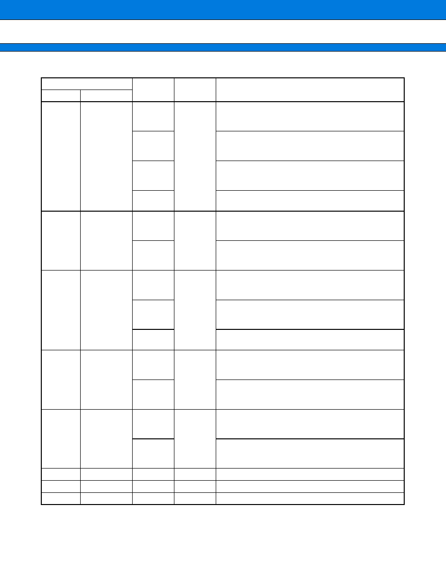
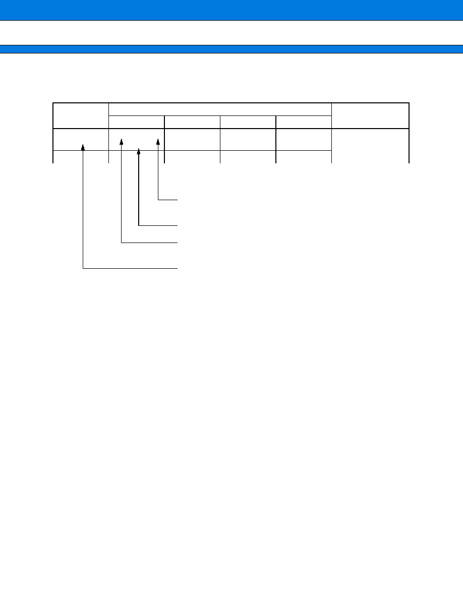
PIN DESCRIPTION
(Continued)
Pin no.
Pin name
Circuit type
Description
LQFP
FLGA
1
A1
SCK2
D
UART2 clock input/output.
This function is valid when corresponding bit of PFR2
register is set to peripheral function.
P26
General purpose input/output port.
This function is valid when corresponding bit of PFR2
register is set to port function.
2
C2
SIN3
D
UART3 data input.
When using this function, corresponding bit of DDR2
register is set to input.
P27
General purpose input/output port.
This function is always valid.
3
C3
SOT3
B
UART3 data output.
This function is valid when corresponding bit of PFR3
register is set to peripheral function.
P30
General purpose input/output port.
This function is valid when corresponding bit of PFR3
register is set to port function.
4
B1
SCK3
B
UART3 clock input/output.
This function is valid when corresponding bit of PFR3
register is set to peripheral function.
P31
General purpose input/output port.
This function is valid when corresponding bit of PFR3
register is set to port function.
5
E4
AIN0
B
Up/down counter 0 AIN input.
When using this function, corresponding bit of DDR3
register is set to input.
P32
General purpose input/output port.
This function is alwais valid.
6
D2
BIN0
B
Up/down counter 0 BIN input.
When using this function, corresponding bit of DDR3
register is set to input.
P33
General purpose input/output port.
This function is always valid.
7
C1
ZIN0
B
Up/down counter 0 ZIN input.
When using this function, corresponding bit of DDR3
register is set to input.
P34
General purpose input/output port.
This function is always valid.
8
D3
AIN1
B
Up/down counter 1 AIN input.
When using this function, corresponding bit of DDR3
register is set to input.
P35
General purpose input/output port.
This function is always valid.
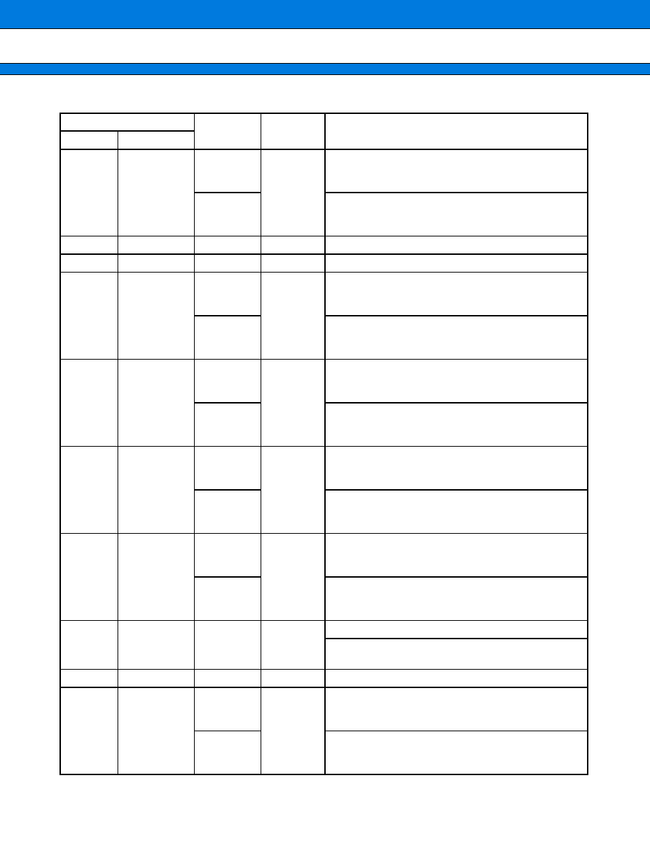
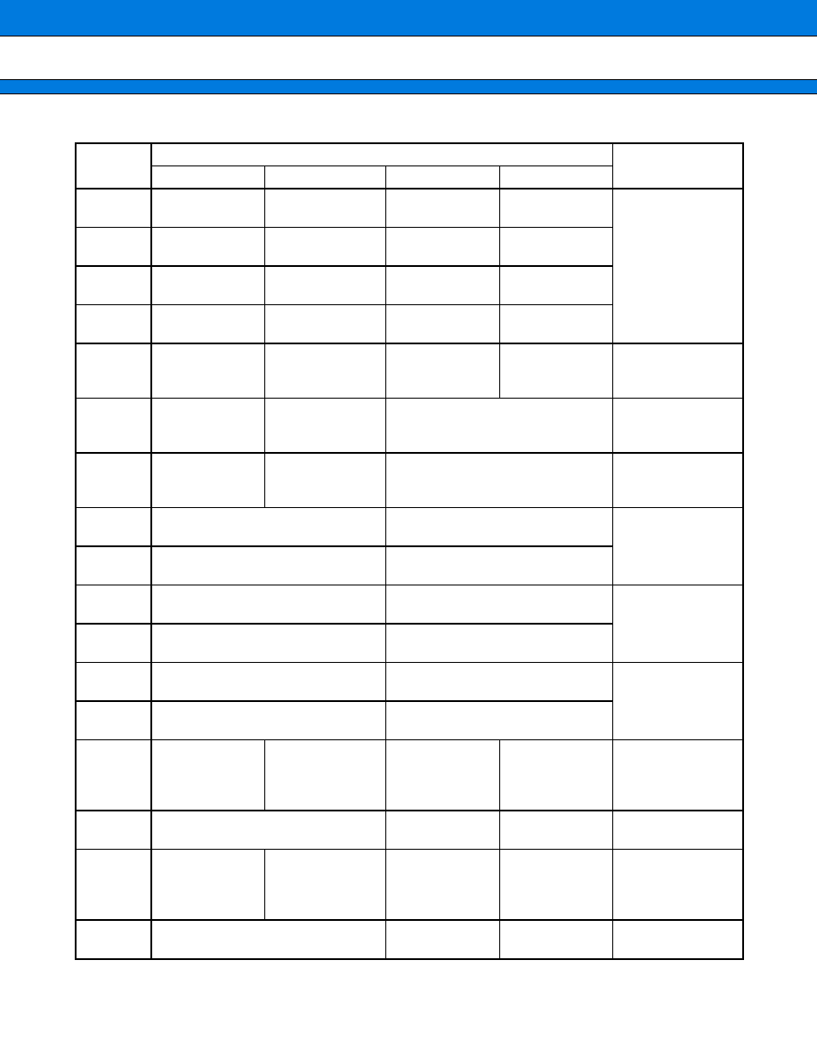
MB91230 Series
8
(Continued)
Pin no.
Pin name
Circuit type
Description
LQFP
FLGA
9
E2
BIN1
B
Up/down counter 1 BIN input.
When using this function, corresponding bit of DDR3
register is set to input.
P36
General purpose input/output port.
This function is always valid.
10
D1
ZIN1
B
Up/down counter 1 ZIN input.
When using this function, corresponding bit of DDR3
register is set to input.
P37
General purpose input/output port.
This function is always valid.
11
F4
PPG0
D
PPG0 output.
This function is valid when corresponding bit of PFR4
register is set to peripheral function.
P40
General purpose input/output port.
This function is valid when corresponding bit of PFR4
register is set to port function.
12
E3
PPG1
D
PPG1 output.
This function is valid when corresponding bit of PFR4
register is set to peripheral function.
P41
General purpose input/output port.
This function is valid when corresponding bit of PFR4
register is set to port function.
13
E1
X0A
Sub-clock oscillation pin (32 kHz)
14
F3
X1A
15
G2
V
CC
3B
Power supply pin for backup (RTC)
16
F1
V
SS
Power supply pin (GND)
17
G4
V
CC
3
Power supply pin (3.3 V internal logic)
18
G1
PPG2
D
PPG2 output.
This function is valid when corresponding bit of PFR4
register is set to peripheral function.
P42
General purpose input/output port.
This function is valid when corresponding bit of PFR4
register is set to port function.
19
H2
PPG3
D
PPG3 output.
This function is valid when corresponding bit of PFR4
register is set to peripheral function.
P43
General purpose input/output port.
This function is valid when corresponding bit of PFR4
register is set to port function.
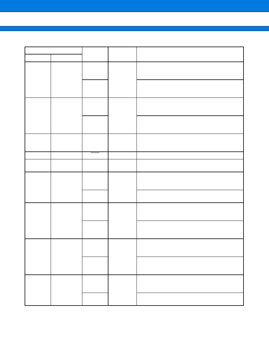
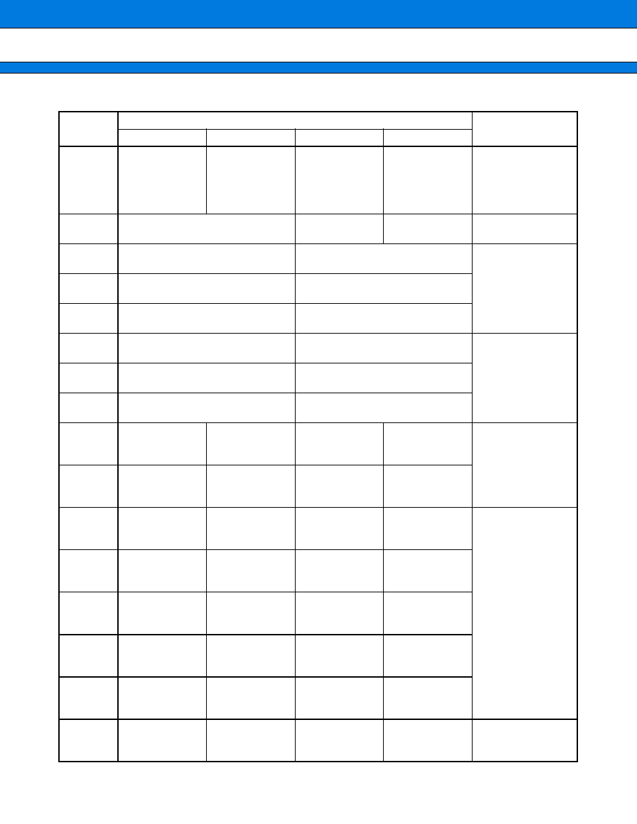
MB91230 Series
9
(Continued)
Pin no.
Pin name
Circuit type
Description
LQFP
FLGA
20
H4
TOT0
D
Reload timer 0 output port.
This function is valid when corresponding bit of PFR4
register is set to peripheral function.
P44
General purpose input/output port.
This function is valid when corresponding bit of PFR4
register is set to port function.
21
H1
TOT1
D
Reload timer 1 output port.
This function is valid when corresponding bit of PFR4
register is set to peripheral function.
P45
General purpose input/output port.
This function is valid when corresponding bit of PFR4
register is set to port function.
22
J2
TOT2
D
Reload timer 2 output port.
This function is valid when corresponding bit of PFR4
register is set to peripheral function.
P46
General purpose input/output port.
This function is valid when corresponding bit of PFR4
register is set to port function.
23
H3
CKOT
D
Clock monitor function output pin.
This function is valid when corresponding bit of PFR4
register is set to peripheral function.
P47
General purpose input/output port.
This function is valid when corresponding bit of PFR4
register is set to port function.
24
J1
INT8
C
External interrupt input.
When using this function, corresponding bit of DDR5
register is set to input.
P50
General purpose input/output port.
This function is always valid.
25
K2
INT9
C
External interrupt input.
When using this function, corresponding bit of DDR5
register is set to input.
P51
General purpose input/output port.
This function is always valid.
26
J3
INT10
C
External interrupt input.
When using this function, corresponding bit of DDR5
register is set to input.
P52
General purpose input/output port.
This function is always valid.
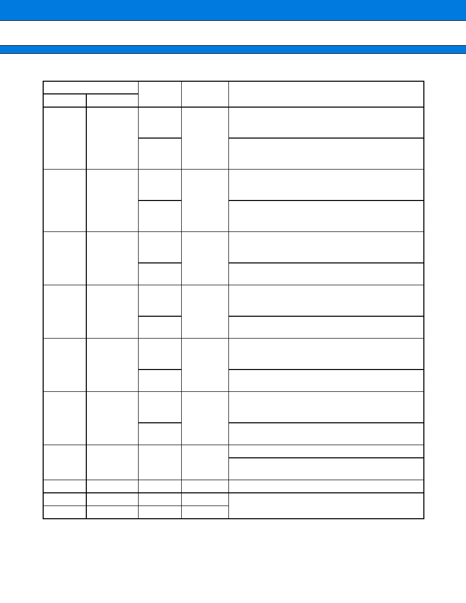
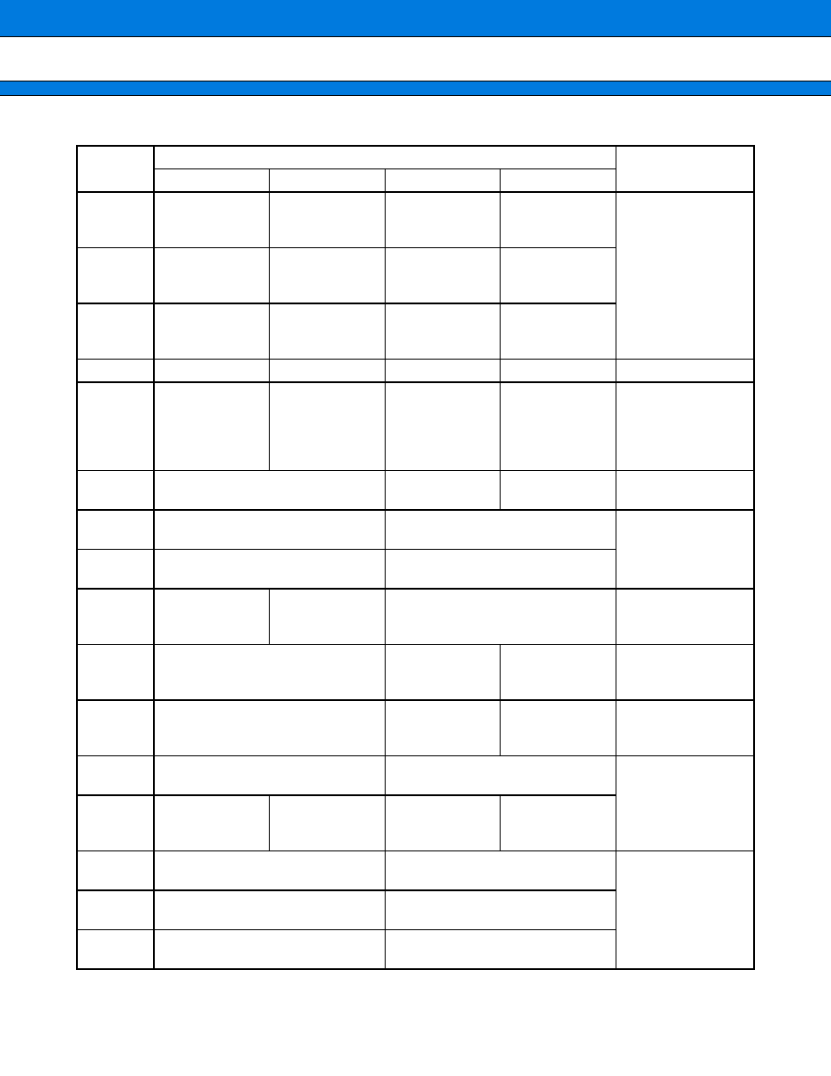
MB91230 Series
10
(Continued)
Pin no.
Pin name
Circuit type
Description
LQFP
FLGA
27
K1
PPG4
C
PPG4 output.
This function is valid when corresponding bit of PFR5
register is set to peripheral function.
INT11
External interrupt input.
This function is enabled when corresponding bit of
PFR5 register is set to port function and corresponding
bit of DDR5 resister is set to input.
P53
General purpose input/output port.
This function is valid when corresponding bit of PFR5
register is set to port function.
28
L2
PPG5
C
PPG5 output.
This function is valid when corresponding bit of PFR5
register is set to peripheral function.
INT12
External interrupt input.
This function is enabled when corresponding bit of
PFR5 register is set to port function and corresponding
bit of DDR5 resister is set to input.
P54
General purpose input/output port.
This function is valid when corresponding bit of PFR5
register is set to port function.
29
J4
TIN2
C
Reload timer 2 event input pin.
This function is valid when corresponding bit of DDR5
register is set to input.
INT13
External interrupt input.
This function is valid when corresponding bit of DDR5
register is set to input.
P55
General purpose input/output port.
This function is always valid.
30
L1
TIN1
C
Reload timer 1 event input pin.
This function is valid when corresponding bit of DDR5
register is set to input.
INT14
External interrupt input.
This function is valid when corresponding bit of DDR5
register is set to input.
P56
General purpose input/output port.
This function is always valid.
MB91230 Series
11
(Continued)
Pin no.
Pin name
Circuit
type
Description
LQFP
FLGA
31
M1
ADTG0
C
External trigger input pin of A/D converter 0.
This function is valid when corresponding bit of DDR5 reg-
ister is set to input.
TIN0
Reload timer 0 event input pin.
This function is valid when corresponding bit of DDR5 reg-
ister is set to input.
INT15
External interrupt input.
This function is valid when corresponding bit of DDR5 reg-
ister is set to input.
P57
General purpose input/output port.
This function is always valid.
32
L3
TOT3
D
Reload timer 3 output port.
This function is valid when corresponding bit of PFRF
register is set to peripheral function.
PF3
General purpose input/output port.
This function is valid when corresponding bit of PFRF
register is set to port function.
33
K3
ADTG1
D
External trigger input pin of A/D converter 1.
This function is valid when corresponding bit of DDRF
register is set to input.
TIN3
Reload timer 3 event input pin.
This function is valid when corresponding bit of DDRF
register is set to input.
PF4
General purpose input/output port.
This function is always valid.
34
M2
DA0
F
D/A converter 0 output pin.
This function is valid when corresponding bit of PFRD
register is set to peripheral function.
PD0
General purpose input/output port.
This function is valid when corresponding bit of PFRD
register is set to port function.
35
J5
DA1
F
D/A converter 1 output pin.
This function is valid when corresponding bit of PFRD
register is set to peripheral function.
PD1
General purpose input/output port.
This function is valid when corresponding bit of PFRD
register is set to port function.
36
L4
AV
CC
Analog power supply (for A/D, D/A converter) .
37
M3
AVRH
Analog reference power supply (for A/D, D/A converter) .
38
K4
AV
SS
GND level input for analog circuit (for A/D, D/A converter) .
MB91230 Series
12
(Continued)
Pin no.
Pin name
Circuit type
Description
LQFP
FLGA
39 to 46
M4, J6, K5,
M5, L6, K6,
L7, M6
AN0 to AN7
E
Analog input pin for A/D converter.
This function is valid when corresponding bit of PFRC
register is set to peripheral function.
PC0 to PC7
General purpose input/output port.
This function is valid when corresponding bit of PFRC
register is set to port function.
47
J7
V
SS
Power supply pin (GND)
48
K7
V
CC
3IO
Power supply pin (analog-shared pin I/O)
49 to 56
L8, J8, M8,
L9, K8, M9,
L10, K9
SEG0 to
SEG7
I
LCD controller/driver LCD segment output pin.
This function is valid when corresponding bit of PFR8
register is set to peripheral function.
P80 to P87
General purpose input/output port.
This function is valid when corresponding bit of PFR8
register is set to port function.
57 to 64
M10, L11, J9,
M11, M12,
K11, K10, L12
SEG8 to
SEG15
I
LCD controller/driver LCD segment output pin.
This function is valid when corresponding bit of PFR9
register is set to peripheral function.
P90 to P97
General purpose input/output port.
This function is valid when corresponding bit of PFR9
register is set to port function.
65 to 72
H9, J11, K12,
J10, H11, J12,
G9, H10
SEG16 to
SEG23
I
LCD controller/driver LCD segment output pin.
This function is valid when corresponding bit of PFRA
register is set to peripheral function.
PA0 to PA7
General purpose input/output port.
This function is valid when corresponding bit of PFRA
register is set to port function.
73, 74
H12, G11
SEG24,
SEG25
I
LCD controller/driver LCD segment output pin.
This function is valid when corresponding bit of PFRB
register is set to peripheral function.
PB0, PB1
General purpose input/output port.
This function is valid when corresponding bit of PFRB
register is set to port function.
75
G10
V
CC
Power supply pin (5 V I/O MB91V230/F233)
Power supply pin (3.3 V internal logic, I/O MB91F233L/
MB91233L)
76
F11
V
SS
Power supply pin (GND)
77, 78
G12, F9
SEG26,
SEG27
I
LCD controller/driver LCD segment output pin.
This function is valid when corresponding bit of PFRB
register is set to peripheral function.
PB2, PB3
General purpose input/output port.
This function is valid when corresponding bit of PFRB
register is set to port function.
MB91230 Series
13
(Continued)
Pin no.
Pin name
Circuit type
Description
LQFP
FLGA
79 to 82
F10, E11, E9,
D11
SEG28 to
SEG31
J
LCD controller/driver LCD segment output pin.
This function is valid when corresponding bit of PFR6
register is set to peripheral function.
P64 to P67
General purpose input/output port. (open-drain)
This function is valid when corresponding bit of PFR6
register is set to port function.
83 to 86
E10, D12,
C11, D10
COM0 to
COM3
I
LCD controller/driver common pins.
This function is valid when corresponding bit of PFR7
register is set to peripheral function.
P70 to P73
General purpose input/output port.
This function is valid when corresponding bit of PFR7
register is set to port function.
87 to 89
C12, B11, D9
MOD2,
MOD1,
MOD0
H
Mode input pin.
90
B12
INIT
G
External reset input.
91 to 94
A12, B10,
C10, A11
V0 to V3
LCD controller/driver reference power supply input
pins.
95
D8
SIN0
D
UART0 data input.
When using this function, corresponding bit of DDR0
register is set to input.
P00
General purpose input/output port.
This function is always valid.
96
B9
SOT0
D
UART0 data output.
This function is valid when corresponding bit of PFR0
register is set to peripheral function.
P01
General purpose input/output port.
This function is valid when corresponding bit of PFR0
register is set to port function.
97
A10
SCK0
D
UART0 clock input/output.
This function is valid when corresponding bit of PFR0
register is set to peripheral function.
P02
General purpose input/output port.
This function is valid when corresponding bit of PFR0
register is set to port function.
98
C9
SIN1
D
UART1 data input.
This function is valid when corresponding bit of DDR0
register is set to input.
P03
General purpose input/output port.
This function is always valid.
MB91230 Series
14
(Continued)
Pin no.
Pin name
Circuit type
Description
LQFP
FLGA
99
B8
SOT1
D
UART1 data output.
This function is valid when corresponding bit of PFR0 reg-
ister is set to peripheral function.
P04
General purpose input/output port.
This function is valid when corresponding bit of PFR0 reg-
ister is set to port function.
100
A9
SCK1
D
UART1 clock input/output.
This function is valid when corresponding bit of PFR0 reg-
ister is set to peripheral function.
P05
General purpose input/output port.
This function is valid when corresponding bit of PFR0 reg-
ister is set to port function.
101
D7
IC0
D
Input capture input 0.
This function is valid when corresponding bit of DDR0
register is set to input.
P06
General purpose input/output port.
This function is always valid.
102
C8
IC1
D
Input capture input 1.
This function is valid when corresponding bit of DDR0
register is set to input.
P07
General purpose input/output port.
This function is always valid.
103
A8
INT0
A
External interrupt input.
This function is valid when corresponding bit of DDR1
register is set to input.
P10
General purpose input/output port.
This function is always valid.
104
B7
INT1
A
External interrupt input.
This function is valid when corresponding bit of DDR1
register is set to input.
P11
General purpose input/output port.
This function is always valid.
105
C7
V
CC
Power supply pin (5 V I/O MB91V230/F233)
Power supply pin (3.3 V internal logic, I/O MB91F233L/
MB91233L)
106
B6
V
SS
Power supply pin (GND)
107
A7
X1
Main-clock oscillation pin
108
C6
X0
MB91230 Series
15
(Continued)
Pin no.
Pin name
Circuit type
Description
LQFP
FLGA
109
A6
INT2
A
External interrupt input.
This function is valid when corresponding bit of DDR1
register is set to input.
P12
General purpose input/output port.
This function is always valid.
110
B5
INT3
A
External interrupt input.
This function is valid when corresponding bit of DDR1
register is set to input.
P13
General purpose input/output port.
This function is always valid.
111
D5
INT4
A
External interrupt input.
This function is valid when corresponding bit of DDR1
register is set to input.
P14
General purpose input/output port.
This function is always valid.
112
B4
INT5
A
External interrupt input.
This function is valid when corresponding bit of DDR1
register is set to input.
P15
General purpose input/output port.
This function is always valid.
113
C5
INT6
A
External interrupt input.
This function is valid when corresponding bit of DDR1
register is set to input.
P16
General purpose input/output port.
This function is always valid.
114
A4
INT7
A
External interrupt input.
This function is valid when corresponding bit of DDR1
register is set to input.
P17
General purpose input/output port.
This function is always valid.
115
B3
CKI0
D
External clock input pin for free-run timer 0.
This function is enabled when corresponding bit of PFR2
register is set to port function and corresponding bit of
DDR2 register is set to input.
OP0
Output compare 0 output pin.
This function is valid when corresponding bit of PFR2
register is set to peripheral function.
P20
General purpose input/output port.
This function is valid when corresponding bit of PFR2
register is set to port function.
MB91230 Series
16
(Continued)
Pin no.
Pin name
Circuit type
Description
LQFP
FLGA
116
C4
CKI1
D
External clock input pin for free-run timer 1.
This function is enabled when corresponding bit of
PFR2 register is set to port function and corresponding
bit of DDR2 register is set to input.
OP1
Output compare1 output pin.
This function is valid when corresponding bit of PFR2
register is set to peripheral function.
P21
General purpose input/output port.
This function is valid when corresponding bit of PFR2
register is set to port function.
117
A3
PWI0
D
Pulse width counter 0 input.
This function is enabled when corresponding bit of
PFR2 register is set to port function and corresponding
bit of DDR2 register is set to input.
OP2
Output compare2 output pin.
This function is valid when corresponding bit of PFR2
register is set to peripheral function.
P22
General purpose input/output port.
This function is valid when corresponding bit of PFR2
register is set to port function.
118
B2
PWI1
D
Pulse width counter 1 input.
This function is enabled when corresponding bit of
PFR2 register is set to port function and corresponding
bit of DDR2 register is set to input.
OP3
Output compare3 output pin.
This function is valid when corresponding bit of PFR2
register is set to peripheral function.
P23
General purpose input/output port.
This function is valid when corresponding bit of PFR2
register is set to port function.
119
D4
SIN2
D
UART2 data input.
This function is valid when corresponding bit of DDR2
register is set to input.
P24
General purpose input/output port.
This function is always valid.
120
A2
SOT2
D
UART2 data output.
This function is valid when corresponding bit of PFR2
register is set to peripheral function.
P25
General purpose input/output port.
This function is valid when corresponding bit of PFR2
register is set to port function.
(38)
L5
AVRL
Analog reference power supply (for A/D converter)
A5, D6, E12,
F2, F12, M7
NC
Unconnected pin.
MB91230 Series
17
s
s
s
s
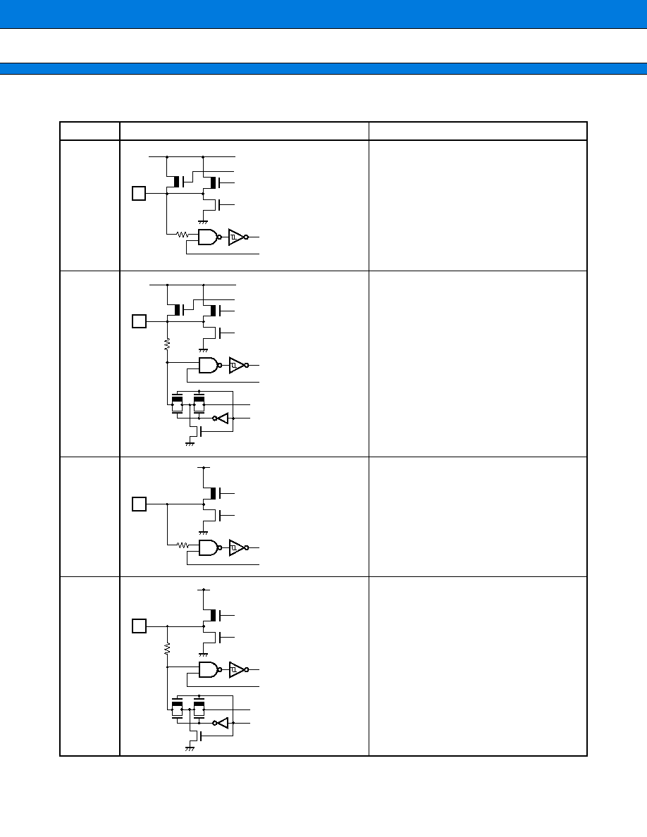
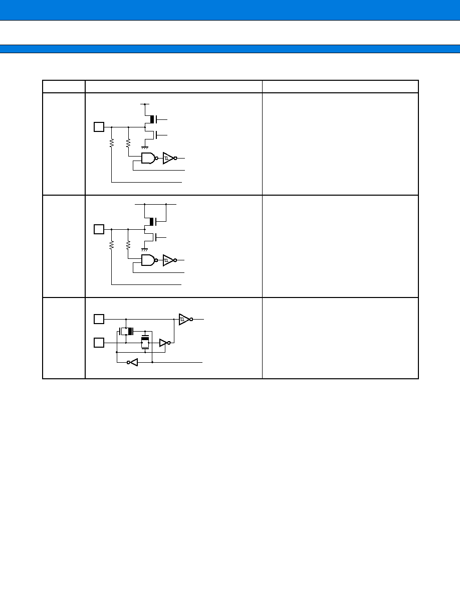
I/O CIRCUIT TYPE
(Continued)
Type
Circuit type
Remarks
A
With Pull-up control (50 k
)
CMOS level output
I
OH
=
4 mA/I
OL
=
4 mA
CMOS hysteresis input (with standby control)
B
With Pull-up control (50 k
)
CMOS level output
I
OH
=
4 mA/I
OL
=
4 mA
CMOS hysteresis input (with standby control)
Test pin for FLASH
C
CMOS level output
CMOS hysteresis input (with standby control)
D
CMOS level output
I
OH
=
4 mA/I
OL
=
4 mA
CMOS hysteresis input (with standby control)
Test pin for FLASH
P
P
N
Pull-up control
Output drive Pch
Output drive Nch
Hysteresis input
Standby control
P
P
N
Pull-up control
Output drive Pch
Output drive Nch
Hysteresis input
Standby control
Test pin for FLASH
Analog SW control
P
N
Output drive Pch
Output drive Nch
Hysteresis input
Standby control
P
N
Output drive Pch
Output drive Nch
Hysteresis input
Standby control
Test pin for FLASH
Analog SW control
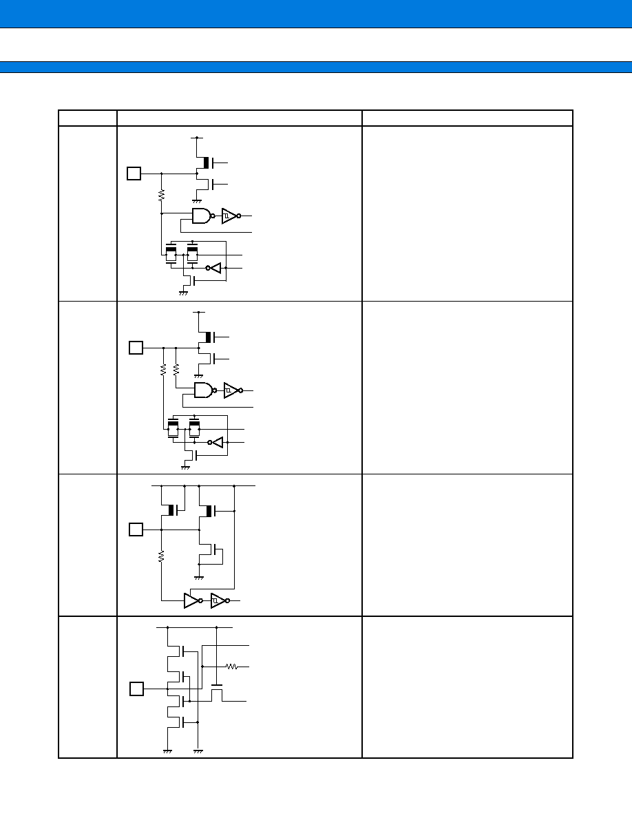
MB91230 Series
18
(Continued)
Type
Circuit type
Remarks
E
CMOS level output
I
OH
=
4 mA/I
OL
=
4 mA
CMOS hysteresis input (with standby control)
Also serving as an analog input
F
CMOS level output
I
OH
=
4 mA/I
OL
=
4 mA
CMOS hysteresis input (with standby control)
Also serving as an analog input
G
With Pull-up control (50 k
)
CMOS hysteresis input
H
High withstand-voltage input
CMOS input (hysteresis level)
P
N
Output drive Pch
Output drive Nch
Hysteresis input
Standby control
Analog input
Analog SW control
P
N
Output drive Pch
Output drive Nch
Hysteresis input
Standby control
Analog input
Analog SW control
P
P
N
Hysteresis input
N
N
N
N
Low impedance input
High impedance input
High voltage
detection
output
MB91230 Series
19
(Continued)
Type
Circuit type
Remarks
I
CMOS level output
I
OH
=
4 mA/I
OL
=
4 mA
CMOS hysteresis input (with standby control)
LCDC output
J
CMOS level output (open-drain)
I
OL
=
20 mA
CMOS hysteresis input (with standby control)
LCDC output
K
Oscillation circuit
P
N
Output drive Pch
Output drive Nch
Hysteresis input
Standby control
LCDC output
P
N
Output drive Nch
Hysteresis input
Standby control
LCDC output
X1
X0
Standby
control
Oscillation
output

MB91230 Series
20
s
s
s
s
HANDLING DEVICES
Preventing Latchup
Latch-up may occur in a CMOS IC if a voltage greater than V
CC
or less than V
SS
is applied to an input or output
pin or if an above-rating voltage is applied between V
CC
and V
SS
.
A latchup, if it occurs, significantly increases the power supply current and may cause thermal destruction of an
element. When you use a CMOS IC, be very careful not to exceed the absolute maximum rating.
Treatment of Unused Pins
Do not leave an unused input pin open, since it may cause a malfunction. Handle by, for example, using a pull-
up or pull-down resistor.
About Power Supply Pins
In products with multiple V
CC
or V
SS
pins, the pins of the same potential are internally connected in the device
to avoid abnormal operations including latch-up. However, you must connect the pins to external power supply
and a ground line to lower the electro-magnetic emission level, to prevent abnormal operation of strobe signals
caused by the rise in the ground level, and to conform to the total output current rating.
Moreover, connect the current supply source with the V
CC
and V
SS
pins of this device at the low impedance.
It is also advisable to connect a ceramic bypass capacitor of approximately 0.1
µ
F between V
CC
and V
SS
near
this device.
About Crystal Oscillator Circuit
Noise near the X0 and X1 pins may cause the device to malfunction. Design the printed circuit board so that
X0, X1, the crystal oscillator (or ceramic oscillator) , and the bypass capacitor to ground are located as close to
the device as possible.
It is strongly recommended to design the PC board artwork with the X0 and X1 pins surrounded by ground plane
because stable operation can be expected with such a layout.
Treatment of NC and OPEN Pins
Pins marked as NC and OPEN must be left open-circuit.
About Mode Pins (MD0 to MD2)
These pins should be connected directly to V
CC
or V
SS
.
To prevent the device erroneously switching to test mode due to noise, design the printed circuit board such that
the distance between the mode pins and V
CC
or V
SS
is as short as possible and the connection impedance is low.
Operation at Start-up
Be sure to execute setting initialized reset (INIT) with INIT pin immediately after start-up.
Also, in order to provide the oscillation stabilization wait time for the oscillation circuit immediately after start-up,
hold the "L" level input to the INIT pin for the required stabilization wait time. (For INIT via the INIT pin, the
oscillation stabilization wait time setting is initialized to the minimum value) .
About Oscillation Input at Power On
When turning the power on, maintain clock input untill the device is released from the oscillation stabilization
wait state.

MB91230 Series
21
Clock Control Block
Input the "L" signal to the INIT pin to assure the clock oscillation stabilization wait time.
Switch Shared Port Function
To switch between the use as a port and the use as a dedicated pin, use the port function register (PFR) .
Low Power Consumption Mode
To enter the standby mode, use the synchronous standby mode (set with the SYNCS bit as bit 8 in the TBCR :
timebse counter control register) and be sure to use the following sequence
In addition, please set I flag, ILM, and ICR to diverge to the interruption handler that is the return factor after the
standby returns.
∑ Please do not do the following when the monitor debugger is used.
∑ Break point setting for above instruction lines
∑ Step execution for above instruction lines
Power-on sequence for dual-power-supply model
∑ Notes on the power-on and power-off sequences
Power-on sequence : Vcc3B, Vcc3
Vcc
Vcc3IO, AVRH, V0-V3
Power-off sequence : Vcc3IO, AVRH, V0-V3 Vcc3
Vcc
Vcc3B, Vcc3
When V
CC
is turned on earlier, a potential difference between V
CC
and V
CC
3 must fall within 3.6 V.
∑ The LCD power supply V3 must not exceed V
CC
in voltage. Apply V3 after turning on V
CC
3.
∑ Turn on V
CC
3 before applying the analog power supply AV
CC
or an analog signal.
(LDI
#value_of_standby, R0) : value_of_standby is write data to STCR.
(LDI
#_STCR, R12)
: _STCR is address (481
H
) of STCR.
STB
R0, @R12
: Writing to standby control register (STCR)
LDUB @R12, R0
: STCR read for synchronous standby
LDUB @R12, R0
: Dummy re-read of STCR
NOP
: NOP
◊
5 for arrangement of timing
NOP
NOP
NOP
NOP

MB91230 Series
22
Notes on the PS register
As the PS register is processed by some instructions in advance, exception handling below may cause the
interrupt handling routine to break when the debugger is used or the display contents of flags in the PS register
to be updated.
As the microcontroller is designed to carry out reprocessing correctly upon returning from such an EIT event, it
performs operations before and after the EIT as specified in either case.
∑ The following operations may be performed when the instruction immediately followed by a DIVOU/DIVOS
instruction is (a) acceptance of a user interrupt, (b) single-stepped, or (c) breaks in response to a data event
or emulator menu :
1) The D0 and D1 flags are updated in advance.
2) An EIT handling routine (user interrupt or emulator) is executed.
3) Upon returning from the EIT, the DIVOU/DIVOS instruction is executed, and the D0 and D1 flags are updated
to the same values as in 1).
∑ The following operations are performed when the ORCCR/STILM/MOVRi and PS instructions are executed
to allow the interrupt.
1) The PS register is updated in advance.
2) An EIT handling routine (user interrupt) is executed.
3) Upon returning from the EIT, the above instructions are executed, and the PS register is updated to the
same value as in 1).
Watchdog Timer
The watchdog timer built in this model monitors a program that it defers a reset within a certain period of time.
The watchdog timer resets the CPU if the program runs out of controls, preventing the reset defer function from
being executed. Once the function of the watchdog timer is enabled, therefore, the watchdog timer keeps on
operating programs until it resets the CPU.
As an exception, the watchdog timer defers a reset automatically under the condition in which the CPU stops
program execution.
For those conditions to which this exception applies, see the function description of watchdog timer.
Step execution of RETI instruction
If an interrupt occurs frequently during step execution, the corresponding interrupt handling routine is executed
repeatedly after step execution. This will prevent the main routine and low-interrupt-level programs from being
executed.
Do not execute step of RETI instruction for escape.
Disable the corresponding interrupt and execute debugger when the corresponding interrupt routine no longer
needs debugging.
Operand Break
Do not apply a data event break to access to the area containing the address of a system stack pointer.
MB91230 Series
23
s
s
s
s
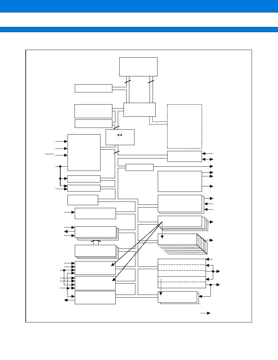
BLOCK DIAGRAM
FR60Lite
CPU Core
32
32
Bit Search
ROM/FLASH
RAM
Bus Converter
External Memory
I/F
(MB91230 is not
supported)
32
16
Adapter
Clock Control
(Clock, Standby,
Reset, Watchdog,
TBT,
Main-Clock-
Stabilization-
Timer)
Clock Monitor
PORT I/F
32
16
Watch Timer
Real Time Clock
Interruption
Controller
LCDC, Driver,
Internal Reference
Voltage
External interrupt
0 to 15
UART
0 to 3
U-TIMER
0 to 3
Up/Down Counter
0, 1
Reload Timer
0 to 3
PPG
0 to 5
4 ch Input
10/8-bit A/D 0
4 ch Input
10/8-bit A/D 1
2 ch Output
8-bit D/A 0, 1
Input Capture 0, 1
Free Run Timer 0
Output Compare 0, 1
Free Run Timer 1
Output Compare 2, 3
8-bit PWC 0, 1
: Trriger signal
X0, X1
MD0 to MD2
INIT
X0A, X1A
V
CC
3B
INT0 to INT15
SIN0 to SIN3
SOT0 to SOT3
SCK0 to SCK3
AN0 to AN3
ADTG
AVRH
AN4 to AN7
ADTG
AV
CC
DA0, DA1
V
CC
PORTs
CKOT
COM0 to COM3
SEG0 to SEG31
V0 to V3
AIN0, AIN1
BIN0, BIN1
ZIN0, ZIN1
TO0 to TO3
PPG0 to PPG5
IC0, IC1
OP0, OP1
CKI0
CKI1
OP2, OP3
PWI0, PWI1
MB91230 Series
24
s
s
s
s
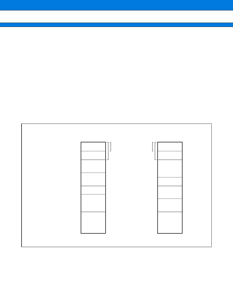
MEMORY SPACE
1.
Memory space
The FR60 Lite family has 4 gigabytes of logical address space (2
32
addresses) available to the CPU by linear
access.
∑ Direct Addressing Areas
The following address space areas are used as I/O areas.
These areas are called direct addressing areas, in which the address of an operand can be specified directly
during an instruction.
The size of directly addressable areas depends on the length of the data being accessed as shown below.
∑
byte data access
: 0 to 0FF
H
∑
half word data access : 0 to 1FF
H
∑
word data access
: 0 to 3FF
H
2.
Memory Map
Note : Do not set the external bus mode in which the MB91230 series cannot operate.
0000 0000
H
0000 0400
H
0001 0000
H
0003 A000
H
0004 0000
H
0008 0000
H
0010 0000
H
FFFF FFFF
H
0001 0000
H
0003 C000
H
0004 0000
H
000C 0000
H
0010 0000
H
FFFF FFFF
H
I/O
I/O
I/O
MB91V230
MB91F233/L, MB91233L
I/O
Direct Addressing
Areas
Access
disallowed
Refer to I/O Map
Access
disallowed
Built-in RAM
24 KB
Access
disallowed
Emulation
SRAM area
512 KB
Access
disallowed
Built-in RAM
16 KB
Access
disallowed
Built-in
FLASH ROM
256 KB
Access
disallowed
MB91230 Series
25
s
s
s
s
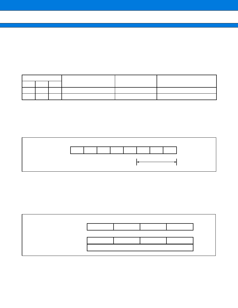
MODE SETTINGS
The FR family uses mode pins (MD2 to MD0) and a mode data to set the operation mode.
∑ Mode Pins
The MD2, MD1, and MD0 pins specify how the mode vector fetch and reset vector fetch is performed.
Setting is prohibited other than that shown in the following table.
∑ Mode data
Data written to the internal mode register (MODR) by a mode vector fetch is called mode data.
After an operation mode has been set in the mode register, the device operates in the operation mode.
The mode data is set by all reset source. User programs cannot set data to the mode register.
Details of mode data description
[bit31 to bit24] Reserved bit
Be sure to set this bit to "00000111".
Operation is not guaranteed when any value other than "00000111" is set.
Note : Mode data set in the mode vector must be placed as byte data at 0x000FFFF8
H
.
Use the highest byte from bit31 to bit24 for placement as the FR family uses the big endian for byte
endian.
Mode Pins
Mode name
Reset vector
access area
Remarks
MD2
MD1
MD0
0
0
0
Internal ROM mode vector
Internal
0
0
1
External ROM mode vector
External
Not supported by this model.
31
bit
30
29
28
27
26
25
24
0
0
0
0
0
1
1
1
Operation mode setting bits
31
bit
24 23
16 15
8 7
0
XXXXXXXX
0x000FFFF8
H
0x000FFFF8
H
0x000FFFFC
H
XXXXXXXX
XXXXXXXX
Mode Data
Mode Data
Reset Vector
XXXXXXXX
XXXXXXXX
XXXXXXXX
Incorrect
Correct
MB91230 Series
26
s
s
s
s
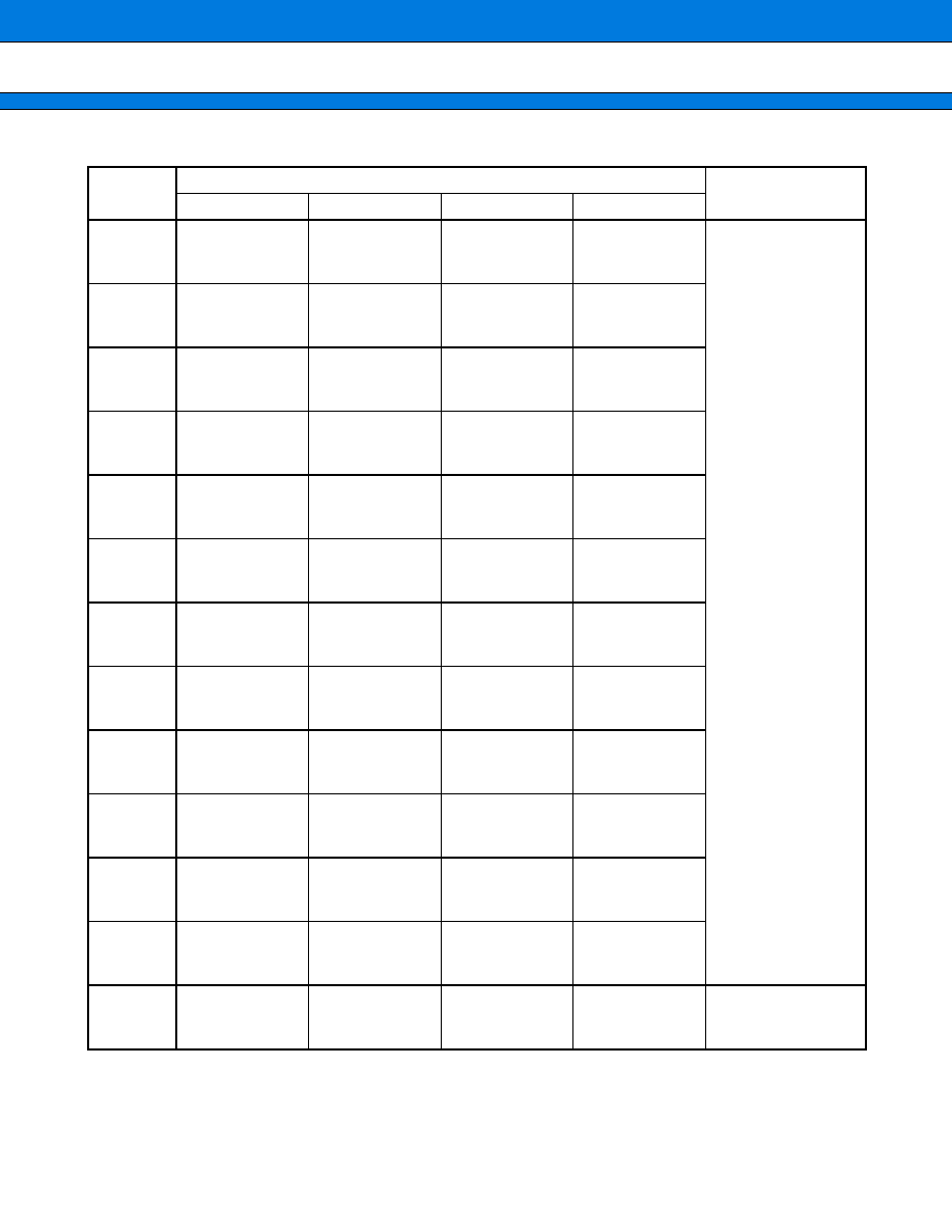
I/O Map
[How to read the table]
Note : Initial values of register bits are represented as follows :
" 1 " : Initial Value " 1 "
" 0 " : Initial Value " 0 "
" X " : Initial Value " undefined"
" - " : No physical register at this location
Access is barred with an undefined data access attribute.
Address
Register
Block
+
0
+
1
+
2
+
3
000000
H
PDR0 [R/W] B
XXXXXXXX
PDR1 [R/W] B
XXXXXXXX
PDR2 [R/W] B
XXXXXXXX
PDR3 [R/W] B
XXXXXXXX
T-unit
Port data register
Read/write attribute Access unit
(B : byte, H : half word, W : word)
Initial value of register after reset
Register name (column 1 of the register is at address 4n, column 2 is
at address 4n
+
1...)
Leftmost register address (For word-length access, column 1 of the
register becomes the MSB of the data.)
MB91230 Series
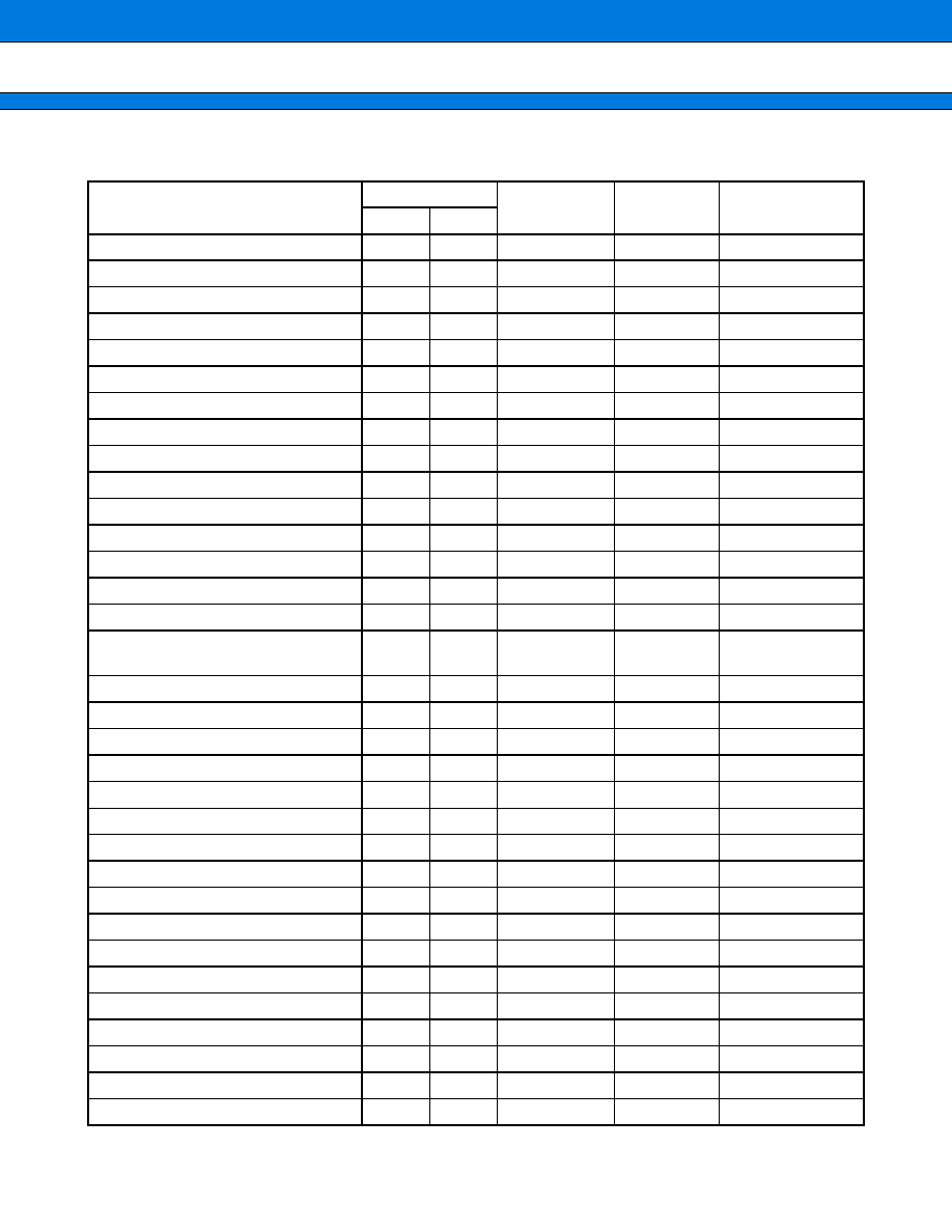
27
(Continued)
Address
Register
Block
+
0
+
1
+
2
+
3
000000
H
PDR0 [R/W] B
XXXXXXXX
PDR1 [R/W] B
XXXXXXXX
PDR2 [R/W] B
XXXXXXXX
PDR3 [R/W] B
XXXXXXXX
Port data register
000004
H
PDR4 [R/W] B
XXXXXXXX
PDR5 [R/W] B
XXXXXXXX
PDR6 [R/W] B
XXXX----
PDR7 [R/W] B
----XXXX
000008
H
PDR8 [R/W] B
XXXXXXXX
PDR9 [R/W] B
XXXXXXXX
PDRA [R/W] B
XXXXXXXX
PDRB [R/W] B
----XXXX
00000C
H
PDRC [R/W] B
XXXXXXXX
PDRD [R/W] B
------XX
PDRF [R/W]
---XX---
000010
H
to
00003C
H
Unused
000040
H
EIRR0 [R/W]
B, H, W
00000000
ENIR0 [R/W]
B, H, W
00000000
ELVR0 [R/W] B, H, W
00000000 00000000
External interrupt
(INT0 to 7)
000044
H
DICR [R/W]
B, H, W
-------0
Delay interrupt
000048
H
TMRLR0 [W] H, W
XXXXXXXX XXXXXXXX
TMR0 [R] H, W
XXXXXXXX XXXXXXXX
Reload timer 0
00004C
H
TMCSR0 [R/W] B, H, W
----0000 00000000
000050
H
TMRLR1 [W] H, W
XXXXXXXX XXXXXXXX
TMR1 [R] H, W
XXXXXXXX XXXXXXXX
Reload timer 1
000054
H
TMCSR1 [R/W] B, H, W
----0000 00000000
000058
H
TMRLR2 [W] H, W
XXXXXXXX XXXXXXXX
TMR2 [R] H, W
XXXXXXXX XXXXXXXX
Reload timer 2
00005C
H
TMCSR2 [R/W] B, H, W
----0000 00000000
000060
H
SSR0 [R/W]
B, H, W
00001000
SIDR0 [R] B, H, W
SODR0 [W] B, H,
W
XXXXXXXX
SCR0 [R/W]
B, H, W
00000100
SMR0 [R/W]
B, H, W
00--0-0-
UART0
000064
H
UTIM0 [R] H (UTIMR0 [W] H)
00000000 00000000
UTIMC0 [R/W] B
0--00001
U-TIMER0
000068
H
SSR1 [R/W]
B, H, W
00001000
SIDR1 [R] B, H, W
SODR1 [W] B, H,
W
XXXXXXXX
SCR1 [R/W]
B, H, W
00000100
SMR1 [R/W]
B, H, W
00--0-0-
UART1
00006C
H
UTIM1 [R] H (UTIMR1 [W] H)
00000000 00000000
UTIMC1 [R/W] B
0--00001
U-TIMER1
MB91230 Series
28
(Continued)
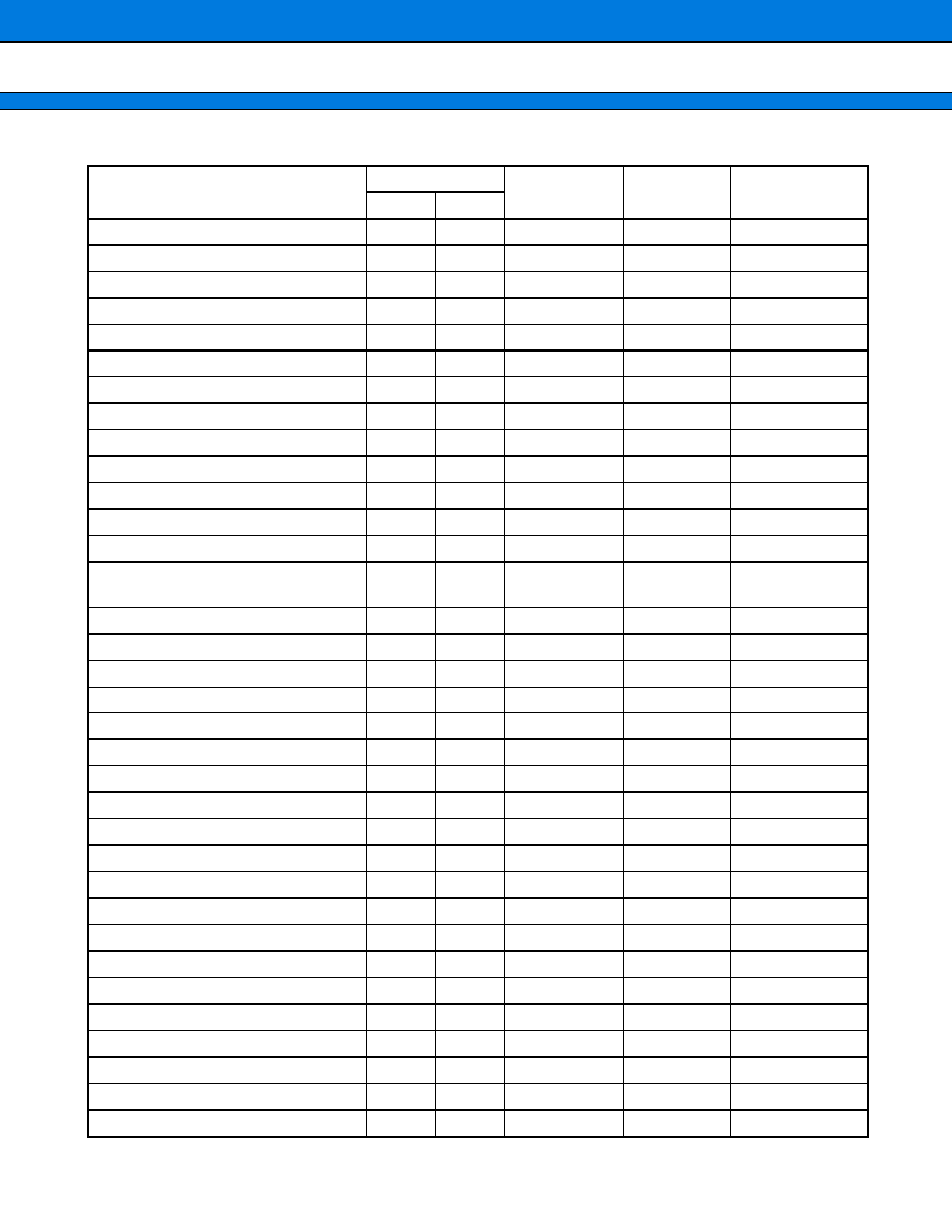
Address
Register
Block
+
0
+
1
+
2
+
3
000070
H
SSR2 [R/W]
B, H, W
00001000
SIDR2 [R] B, H,
W
SODR2 [W] B, H,
W
XXXXXXXX
SCR2 [R/W]
B, H, W
00000100
SMR2 [R/W]
B, H, W
00--0-0-
UART2
000074
H
UTIM2 [R] H (UTIMR1 [W] H)
00000000 00000000
UTIMC2 [R/W] B
0--00001
U-TIMER2
000078
H
ADCS0 [R/W] H, W
XXXXXXXX XXXXXXXX
ADCT0 [R/W] H, W
000-0000 -000--00
A/D converter 0
(series-parallel type)
00007C
H
ADT00 (ADTH0/ADTL0) [R] H, W
000000XX XXXXXXXX
ADT01 (ADTH1/ADTL1) [R] H, W
000000XX XXXXXXXX
000080
H
ADT02 (ADTH2/ADTL2) [R] H, W
000000XX XXXXXXXX
ADT03 (ADTH3/ADTL3) [R] H, W
000000XX XXXXXXXX
000084
H
ADCS1 [R/W] H, W
XXXXXXXX XXXXXXXX
ADCT1 [R/W] H, W
000-0000 --000--00
A/D converter 1
(series-parallel type)
000088
H
ADT10 (ADTH0/ADTL0) [R] H, W
000000XX XXXXXXXX
ADT11 (ADTH1/ADTL1) [R] H, W
000000XX XXXXXXXX
00008C
H
ADT12 (ADTH2/ADTL2) [R] H, W
000000XX XXXXXXXX
ADT13 (ADTH3/ADTL3) [R] H, W
000000XX XXXXXXXX
000090
H
DACR1 [R/W]
B, H, W
-------0
DACR0 [R/W]
B, H, W
-------0
D/A converter
000094
H
DADR1 [R/W]
B, H, W
XXXXXXXX
DADR0 [R/W]
B, H, W
XXXXXXXX
000098
H
LCDCMR [R/W]
B, H, W
----0000
LCR0 [R/W]
B, H, W
00010000
LCR1 [R/W]
B, H, W
00000000
LCD controller/driver
00009C
H
VRAM0 [R/W]
B, H, W
XXXXXXXX
VRAM1 [R/W]
B, H, W
XXXXXXXX
VRAM2 [R/W]
B, H, W
XXXXXXXX
VRAM3 [R/W]
B, H, W
XXXXXXXX
0000A0
H
VRAM4 [R/W]
B, H, W
XXXXXXXX
VRAM5 [R/W]
B, H, W
XXXXXXXX
VRAM6 [R/W]
B, H, W
XXXXXXXX
VRAM7 [R/W]
B, H, W
XXXXXXXX
0000A4
H
VRAM8 [R/W]
B, H, W
XXXXXXXX
VRAM9 [R/W]
B, H, W
XXXXXXXX
VRAM10 [R/W]
B, H, W
XXXXXXXX
VRAM11 [R/W]
B, H, W
XXXXXXXX
0000A8
H
VRAM12 [R/W]
B, H, W
XXXXXXXX
VRAM13 [R/W]
B, H, W
XXXXXXXX
VRAM14 [R/W]
B, H, W
XXXXXXXX
VRAM15 [R/W]
B, H, W
XXXXXXXX
0000AC
H
CKR [R/W]
B, H, W
----0000
Clock monitor
MB91230 Series
29
(Continued)
Address
Register
Block
+
0
+
1
+
2
+
3
0000B0
H
RCR1 [W]
B, H, W
00000000
RCR0 [W]
B, H, W
00000000
UDCR1 [R]
B, H, W
00000000
UDCR0 [R]
B, H, W
00000000
Up/down counter0, 1
0000B4
H
CCRH0 [R/W]
B, H, W
00000000
CCRL0 [R/W]
B, H, W
00001000
CSR0 [R/W]
B, H, W
00000000
0000B8
H
CCRH1 [R/W]
B, H, W
00000000
CCRL1 [R/W]
B, H, W
00001000
CSR1 [R/W]
B, H, W
00000000
0000BC
H
unused
0000C0
H
SSR [R/W]
B, H, W
00001000
SIDR 3 [R] B, H,
W
SODR 3 [W] B, H,
W
XXXXXXXX
SCR [R/W]
B, H, W
00000100
SMR [R/W]
B, H, W
00--0-0-
UART3
0000C4
H
UTIM [R] H (UTIMR [W] H)
00000000 00000000
UTIMC [R/W] B
0--00001
U-TIMER3
0000C8
H
TMRLR3 [W] H, W
XXXXXXXX XXXXXXXX
TMR3 [R] H, W
XXXXXXXX XXXXXXXX
Reload
timer 3
0000CC
H
TMCSR3 [R/W] B, H, W
---00000 00000000
0000D0
H
EIRR1 [R/W]
B, H, W
00000000
ENIR1 [R/W]
B, H, W
00000000
ELVR1 [R/W] B, H, W
00000000 00000000
External interrupt
(INT8 to 16)
0000D4
H
TCDT0 [R/W] H, W
00000000 00000000
TCCS0 [R/W]
B, H, W
00000000
Free-run timer 0
0000D8
H
TCDT1 [R/W] H, W
00000000 00000000
TCCS1 [R/W]
B, H, W
00000000
Free-run timer 1
0000DC
H
IPCP1 [R] H, W
XXXXXXXX XXXXXXXX
IPCP0 [R] H, W
XXXXXXXX XXXXXXXX
Input capture
0000E0
H
ICS01 [R/W]
B, H, W
00000000
0000E4
H
OCCP1 [R/W] H, W
XXXXXXXX XXXXXXXX
OCCP0 [R/W] H, W
XXXXXXXX XXXXXXXX
Output compare
0000E8
H
OCCP3 [R/W] H, W
XXXXXXXX XXXXXXXX
OCCP2 [R/W] H, W
XXXXXXXX XXXXXXXX
0000EC
H
OCS23 [R/W] B, H, W
---0--00 0000--00
OCS01 [R/W] B, H, W
---0-00 0000--00

MB91230 Series
30
(Continued)
Address
Register
Block
+
0
+
1
+
2
+
3
0000F0
H
PWCC0 [R/W]
B, H, W
0---00-0
PWCD0 [R]
B, H, W
XXXXXXXX
PWCC1 [R/W]
B, H, W
0---00-0
PWCD1 [R]
B, H, W
XXXXXXXX
PWC0, 1
0000F4
H
WTDBL [R/W] B
-------0
WTCR [R/W] B, H
00000000 000-00-X
Real-time clock
0000F8
H
WTBR0 [R/W] B
---XXXXX
WTBR1 [R/W] B
XXXXXXXX
WTBR2 [R/W] B
XXXXXXXX
0000FC
H
WTHR [R/W]
B, H
---XXXXX
WTMR [R/W]
B, H
--XXXXXX
WTSR [R/W] B
--XXXXXX
000100
H
to
000114
H
Unused
000118
H
GCN10 [R/W] H
00110010 00010000
GCN20 [R/W] B
00000000
PPG
00011C
H
Unused
000120
H
PTMR0 [R] H, W
11111111 11111111
PCSR0 [W] H, W
XXXXXXXX XXXXXXXX
PPG0
000124
H
PDUT0 [W] H, W
XXXXXXXX XXXXXXXX
PCNH0 [R/W]
B, H, W
00000000
PCNL0 [R/W]
B, H, W
00000000
000128
H
PTMR1 [R] H, W
11111111 11111111
PCSR1 [W] H, W
XXXXXXXX XXXXXXXX
PPG1
00012C
H
PDUT1 [W] H, W
XXXXXXXX XXXXXXXX
PCNH1 [R/W]
B, H, W
00000000
PCNL1 [R/W]
B, H, W
00000000
000130
H
PTMR2 [R] H, W
11111111 11111111
PCSR2 [W] H, W
XXXXXXXX XXXXXXXX
PPG2
000134
H
PDUT2 [W] H, W
XXXXXXXX XXXXXXXX
PCNH2 [R/W]
B, H, W
00000000
PCNL2 [R/W]
B, H, W
00000000
000138
H
PTMR3 [R] H, W
11111111 11111111
PCSR3 [W] H, W
XXXXXXXX XXXXXXXX
PPG3
00013C
H
PDUT3 [W] H, W
XXXXXXXX XXXXXXXX
PCNH3 [R/W]
B, H, W
00000000
PCNL3 [R/W]
B, H, W
00000000
000140
H
PTMR4 [R] H, W
11111111 11111111
PCSR4 [W] H, W
XXXXXXXX XXXXXXXX
PPG4
000144
H
PDUT4 [W] H, W
XXXXXXXX XXXXXXXX
PCNH4 [R/W]
B, H, W
00000000
PCNL4 [R/W]
B, H, W
00000000

MB91230 Series
31
(Continued)
Address
Register
Block
+
0
+
1
+
2
+
3
000148
H
PTMR5 [R] H, W
11111111 11111111
PCSR5 [W] H, W
XXXXXXXX XXXXXXXX
PPG5
00014C
H
PDUT5 [W] H, W
XXXXXXXX XXXXXXXX
PCNH5 [R/W]
B, H, W
00000000
PCNL5 [R/W]
B, H, W
00000000
000150
H
to
0001FC
H
Unused
000200
H
to
0003EC
H
Unused
0003F0
H
BSD0 [W] W
XXXXXXXX XXXXXXXX XXXXXXXX XXXXXXXX
Bit search
0003F4
H
BSD1 [R/W] W
XXXXXXXX XXXXXXXX XXXXXXXX XXXXXXXX
0003F8
H
BSDC [W] W
XXXXXXXX XXXXXXXX XXXXXXXX XXXXXXXX
0003FC
H
BSRR [R] W
XXXXXXXX XXXXXXXX XXXXXXXX XXXXXXXX
000400
H
DDR0 [R/W] B
00000000
DDR1 [R/W] B
00000000
DDR2 [R/W] B
00000000
DDR3 [R/W]
B00000000
Data direction
register
000404
H
DDR4 [R/W] B
00000000
DDR5 [R/W] B
00000000
DDR6 [R/W] B
0000----
DDR7 [R/W] B
----0000
000408
H
DDR8 [R/W] B
00000000
DDR9 [R/W] B
00000000
DDRA [R/W] B
00000000
DDRB [R/W] B
----0000
00040C
H
DDRC [R/W] B
00000000
DDRD [R/W] B
------00
DDRF [R/W] B
---00---
000410
H
to
00041C
H
Unused
000420
H
PFR0 [R/W] B
--00-00-
PFR1 [R/W] B
--------
PFR2 [R/W] B
-00-0000
PFR3 [R/W] B
------00
Port function register
000424
H
PFR4 [R/W] B
00000000
PFR5 [R/W] B
---00---
PFR6 [R/W] B
0000----
PFR7 [R/W] B
----0000
000428
H
PFR8 [R/W] B
00000000
PFR9 [R/W] B
00000000
PFRA [R/W] B
00000000
PFRB [R/W] B
----0000
00042C
H
PFRC [R/W] B
--------
PFRD [R/W] B
------00
PFRF [R/W] B
----0---
000430
H
to
00043C
H
Unused
MB91230 Series
32
(Continued)
Address
Register
Block
+
0
+
1
+
2
+
3
000440
H
ICR00 [R/W]
B, H, W
---11111
ICR01 [R/W]
B, H, W
---11111
ICR02 [R/W]
B, H, W
---11111
ICR03 [R/W]
B, H, W
---11111
Interrupt control unit
000444
H
ICR04 [R/W]
B, H, W
---11111
ICR05 [R/W]
B, H, W
---11111
ICR06 [R/W]
B, H, W
---11111
ICR07 [R/W]
B, H, W
---11111
000448
H
ICR08 [R/W]
B, H, W
---11111
ICR09 [R/W]
B, H, W
---11111
ICR10 [R/W]
B, H, W
---11111
ICR11 [R/W]
B, H, W
---11111
00044C
H
ICR12 [R/W]
B, H, W
---11111
ICR13 [R/W]
B, H, W
---11111
ICR14 [R/W]
B, H, W
---11111
ICR15 [R/W]
B, H, W
---11111
000450
H
ICR16 [R/W]
B, H, W
---11111
ICR17 [R/W]
B, H, W
---11111
ICR18 [R/W]
B, H, W
---11111
ICR19 [R/W]
B, H, W
---11111
000454
H
ICR20 [R/W]
B, H, W
---11111
ICR21 [R/W]
B, H, W
---11111
ICR22 [R/W]
B, H, W
---11111
ICR23 [R/W]
B, H, W
---11111
000458
H
ICR24 [R/W]
B, H, W
---11111
ICR25 [R/W]
B, H, W
---11111
ICR26 [R/W]
B, H, W
---11111
ICR27 [R/W]
B, H, W
---11111
00045C
H
ICR28 [R/W]
B, H, W
---11111
ICR29 [R/W]
B, H, W
---11111
ICR30 [R/W]
B, H, W
---11111
ICR31 [R/W]
B, H, W
---11111
000460
H
ICR32 [R/W]
B, H, W
---11111
ICR33 [R/W]
B, H, W
---11111
ICR34 [R/W]
B, H, W
---11111
ICR35 [R/W]
B, H, W
---11111
000464
H
ICR36 [R/W]
B, H, W
---11111
ICR37 [R/W]
B, H, W
---11111
ICR38 [R/W]
B, H, W
---11111
ICR39 [R/W]
B, H, W
---11111
000468
H
ICR40 [R/W]
B, H, W
---11111
ICR41 [R/W]
B, H, W
---11111
ICR42 [R/W]
B, H, W
---11111
ICR43 [R/W]
B, H, W
---11111
00046C
H
ICR44 [R/W]
B, H, W
---11111
ICR45 [R/W]
B, H, W
---11111
ICR46 [R/W]
B, H, W
---11111
ICR47 [R/W]
B, H, W
---11111
000470
H
to
00047C
H
Unused

MB91230 Series
33
(Continued)
* : This register is set when the mode vector is fetched. Not user-accessible.
Address
Register
Block
+
0
+
1
+
2
+
3
000480
H
RSRR [R/W]
B, H, W
10000000
STCR [R/W]
B, H, W
00110011
TBCR [R/W]
B, H, W
00XXXX00
CTBR [W]
B, H, W
XXXXXXXX
Clock control
000484
H
CLKR [R/W]
B, H, W
00000000
WPR [R/W]
B, H, W
XXXXXXXX
DIVR0 [R/W]
B, H, W
00000011
DIVR1 [R/W]
B, H, W
00000000
000488
H
OSCCR [R/W] B
XXXXXXX0
00048C
H
WPCR [R/W] B
00---000
Watch timer
000490
H
OSCR [R/W] B
00---000
Main clock oscillation
stabilization wait timer
000494
H
to
0004FC
H
Unused
000500
H
PCR1 [R/W] B
00000000
PCR3 [R/W] B
00000000
Pull-up control
register
000504
H
to
00051C
H
Unused
000520
H
to
0007F8
H
Unused
0007FC
H
MODR*
XXXXXXXX
Operation mode
000800
H
to
000AFC
H
Unused
000B00
H
to
000FFC
H
Unused
001000
H
to
001FFC
H
Unused
MB91230 Series
34
s
s
s
s
INTERRUPT VECTOR
(Continued)
Interrupt source
Interrupt number
Interrupt level
Offset
TBR default
address
10
16
Reset
0
00
3FC
H
000FFFFC
H
Mode vector
1
01
3F8
H
000FFFF8
H
System reserved
2
02
3F4
H
000FFFF4
H
System reserved
3
03
3F0
H
000FFFF0
H
System reserved
4
04
3EC
H
000FFFEC
H
System reserved
5
05
3E8
H
000FFFE8
H
System reserved
6
06
3E4
H
000FFFE4
H
Coprocessor absent trap
7
07
3E0
H
000FFFE0
H
Coprocessor error trap
8
08
3DC
H
000FFFDC
H
INTE instruction
9
09
3D8
H
000FFFD8
H
Instruction break exception
10
0A
3D4
H
000FFFD4
H
Operand break trap
11
0B
3C0
H
000FFFD0
H
Step trace trap
12
0C
3CC
H
000FFFCC
H
NMI request (tool)
13
0D
3C8
H
000FFFC8
H
Undefined instruction exception
14
0E
3C4
H
000FFFC4
H
NMI request
(This model has no NMI request)
15
0F
15 (F
H
) fixed
3C0
H
000FFFC0
H
External interrupt 0
16
10
ICR00
3BC
H
000FFFBC
H
External interrupt 1
17
11
ICR01
3B8
H
000FFFB8
H
External interrupt 2
18
12
ICR02
3B4
H
000FFFB4
H
External interrupt 3
19
13
ICR03
3B0
H
000FFFB0
H
External interrupt 4
20
14
ICR04
3AC
H
000FFFAC
H
External interrupt 5
21
15
ICR05
3A8
H
000FFFA8
H
External interrupt 6
22
16
ICR06
3A4
H
000FFFA4
H
External interrupt 7
23
17
ICR07
3A0
H
000FFFA0
H
Reload timer 0
24
18
ICR08
39C
H
000FFF9C
H
Reload timer 1
25
19
ICR09
398
H
000FFF98
H
Reload timer 2
26
1A
ICR10
394
H
000FFF94
H
UART0(Reception completed)
27
1B
ICR11
390
H
000FFF90
H
UART0 (Transmission completed)
28
1C
ICR12
38C
H
000FFF8C
H
UART1 (Reception completed)
29
1D
ICR13
388
H
000FFF88
H
UART1 (Transmission completed)
30
1E
ICR14
384
H
000FFF84
H
UART2 (Reception completed)
31
1F
ICR15
380
H
000FFF80
H
UART2 (Transmission completed)
32
20
ICR16
37C
H
000FFF7C
H
MB91230 Series
35
(Continued)
Interrupt source
Interrupt number
Interrupt level
Offset
TBR default
address
10
16
UART3 (Reception completed)
33
21
ICR17
378
H
000FFF78
H
UART3 (Transmission completed)
34
22
ICR18
374
H
000FFF74
H
A/D ch0
35
23
ICR19
370
H
000FFF70
H
A/D ch1
36
24
ICR20
36C
H
000FFF6C
H
External interrupt8
37
25
ICR21
368
H
000FFF68
H
External interrupt9
38
26
ICR22
364
H
000FFF64
H
External interrupt 10
39
27
ICR23
360
H
000FFF60
H
External interrupt 11
40
28
ICR24
35C
H
000FFF5C
H
External interrupt 12
41
29
ICR25
358
H
000FFF58
H
External interrupt 13
42
2A
ICR26
354
H
000FFF54
H
External interrupt 14
43
2B
ICR27
350
H
000FFF50
H
External interrupt 15
44
2C
ICR28
34C
H
000FFF4C
H
Real-time clock
45
2D
ICR29
348
H
000FFF48
H
Main clock oscillation
stabilization wait timer
46
2E
ICR30
344
H
000FFF44
H
Timebase timer 0 overflow
47
2F
ICR31
340
H
000FFF40
H
Reload timer 3
48
30
ICR32
33C
H
000FFF3C
H
Watch timer
49
31
ICR33
338
H
000FFF38
H
UD Counter 0
50
32
ICR34
334
H
000FFF34
H
UD Counter 1
51
33
ICR35
330
H
000FFF30
H
PPG 0/1
52
34
ICR36
32C
H
000FFF2C
H
PPG 2/3
53
35
ICR37
328
H
000FFF28
H
PPG 4/5
54
36
ICR38
324
H
000FFF24
H
Free-run timer 0
55
37
ICR39
320
H
000FFF20
H
Free-run timer 1
56
38
ICR40
31C
H
000FFF1C
H
ICU 0 (capture)
57
39
ICR41
318
H
000FFF18
H
ICU 1 (capture)
58
3A
ICR42
314
H
000FFF14
H
OCU 0 (match)
59
3B
ICR43
310
H
000FFF10
H
OCU 1 (match)
60
3C
ICR44
30C
H
000FFF0C
H
OCU 2 (match)
61
3D
ICR45
308
H
000FFF08
H
OCU 3 (match)
62
3E
ICR46
304
H
000FFF04
H
Delay interrupt source bit
63
3F
ICR47
300
H
000FFF00
H
System reserved (Used by REALOS)
64
40
2FC
H
000FFEFC
H
System reserved (Used by REALOS)
65
41
2F8
H
000FFEF8
H
System reserved
66
42
2F4
H
000FFEF4
H
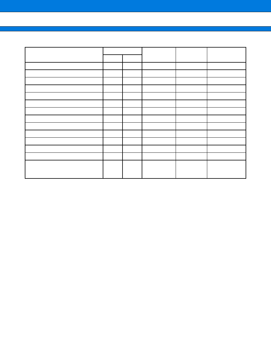
MB91230 Series
36
(Continued)
Interrupt source
Interrupt number
Interrupt level
Offset
TBR default
address
10
16
System reserved
67
43
2F0
H
000FFEF0
H
System reserved
68
44
2EC
H
000FFEEC
H
System reserved
69
45
2E8
H
000FFEE8
H
System reserved
70
46
2E4
H
000FFEE4
H
System reserved
71
47
2E0
H
000FFEE0
H
System reserved
72
48
2DC
H
000FFEDC
H
System reserved
73
49
2D8
H
000FFED8
H
System reserved
74
4A
2D4
H
000FFED4
H
System reserved
75
4B
2D0
H
000FFED0
H
System reserved
76
4C
2CC
H
000FFECC
H
System reserved
77
4D
2C8
H
000FFEC8
H
System reserved
78
4E
2C4
H
000FFEC4
H
System reserved
79
4F
2C0
H
000FFEC0
H
Used by INT instruction
80
to
255
50
to
FF
2BC
H
to
000
H
000FFEBC
H
to
000FFC00
H

MB91230 Series
37
s
s
s
s
PIN STATUS IN EACH CPU STATE
Terms used as the status of pins mean as follows.
∑ Input enabled
Indicates that the input function can be used.
∑ Input 0 fixed
Indicates that the input level has been internally fixed to be "0" to prevent leakage when the input is released.
∑ Output Hi-Z
Means the placing of a pin in a high impedance state by preventing the transistor for driving the pin from driving.
∑ Output is maintained
Indicates the output in the output state existing immediately before this mode is established. If the device
enters this mode with an internal output peripheral operating or while serving as an output port, the output is
performed by the internal peripheral or the port output is maintained, respectively.
∑ State existing immediately before is maintained
When the device serves for output or input immediately before entering this mode, the device maintains the
output or is ready for the input, respectively.
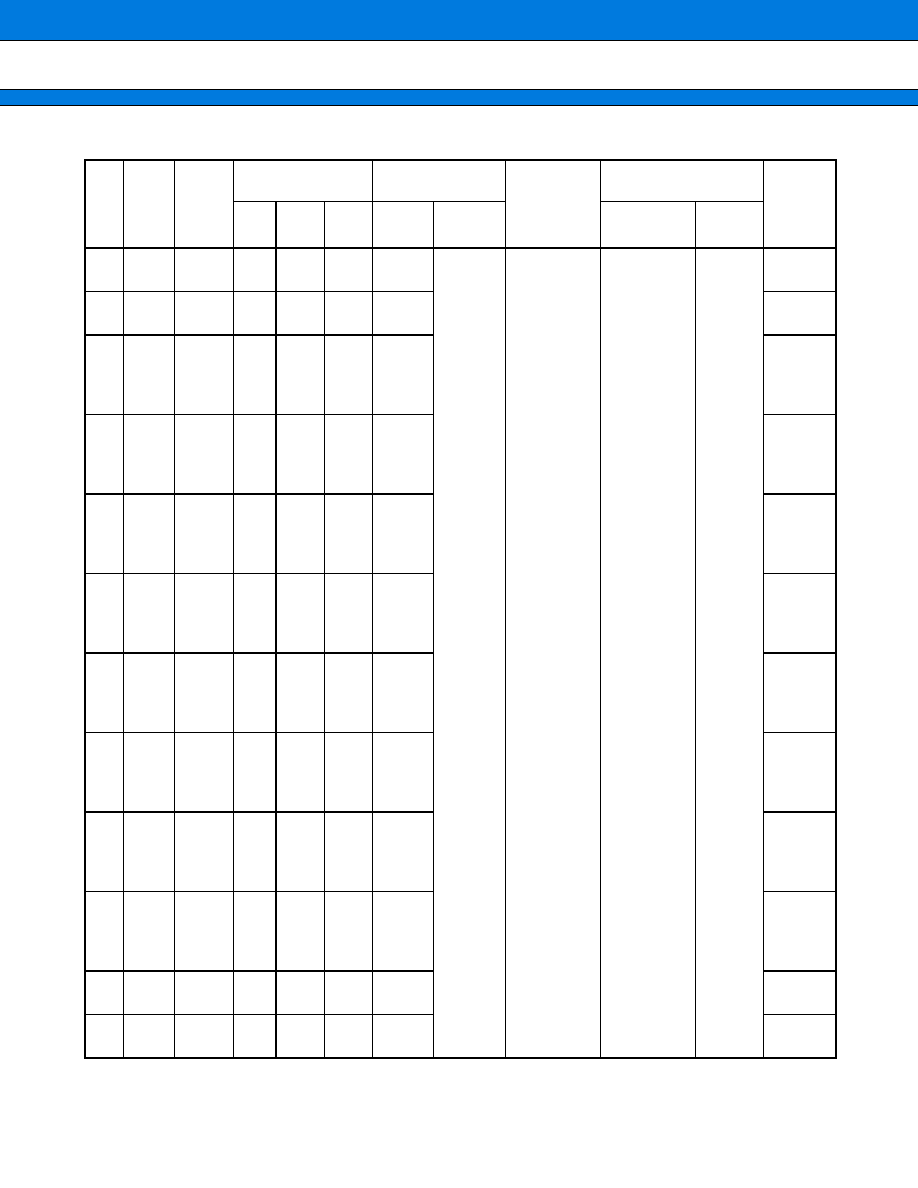
MB91230 Series
38
∑
Pin Status List
(Continued)
Pin
no.
Pin
name
Port
name
Specified function
name
At initializing
At sleep
mode
At Stop mode
Remarks
Input
Output
Input/
Output
Function
name
Reset
initializa-
tion
HIZ
=
0
HIZ
=
1
1
P26/
SCK2
P26
SCK2 P26
Output
Hi-Z/
Input
enabled
Retention
of the
immediately
prior state
Retention
of the
immediately
prior state
Output
Hi-Z/
Input 0
fixed
2
P27/
SIN3
P27
SIN3
P27
3
P30/
SOT3
P30
SOT3
P30
Pull-up
options
can be
selected
4
P31/
SCK3
P31
SCK3 P31
Pull-up
options
can be
selected
5
P32/
AIN0
P32
AIN0
P32
Pull-up
options
can be
selected
6
P33/
BIN0
P33
BIN0
P33
Pull-up
options
can be
selected
7
P34/
ZIN0
P34
ZIN0
P34
Pull-up
options
can be
selected
8
P35/
AIN1
P35
AIN1
P35
Pull-up
options
can be
selected
9
P36/
BIN1
P36
BIN1
P36
Pull-up
options
can be
selected
10
P37/
ZIN1
P37
ZIN1
P37
Pull-up
options
can be
selected
11
P40/
PPG0
P40
PPG
0
P40
12
P41/
PPG1
P41
PPG
1
P41
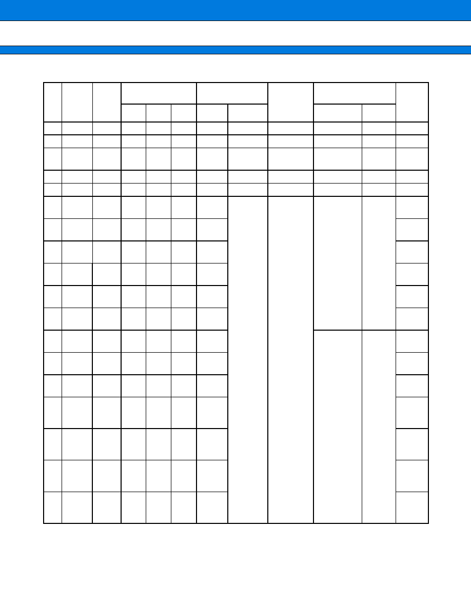
MB91230 Series
39
Note : P : Port selected, F : Specified function selected
(Continued)
Pin
no.
Pin
name
Port
name
Specified function
name
At initializing
At sleep
mode
At Stop mode
Remarks
Input
Output
Input/
Output
Function
name
Reset
initialization
HIZ
=
0
HIZ
=
1
13 X0A
14 X1A
15
V
CC
3B/
V
CC
16 V
SS
17 V
CC
3
18
P42/
PPG2
P42
PPG2
P42
Output
Hi-Z/
Input
enabled
Retention
of the
immediately
prior state
Retention
of the
immediately
prior state
Output
Hi-Z/
Input 0
fixed
19
P43/
PPG3
P43
PPG3
P43
20
P44/
TOT0
P44
TOT0
P44
21
P45/
TOT1
P45
TOT1
P45
22
P46/
TOT2
P46
TOT2
P46
23
P47/
CKOT
P47
CKOT
P47
24
P50/
INT8
P50
INT8
P50
P :
Retention
of the
immediately
prior state
F :
Input
enabled
P :
Output
Hi-Z
F :
Input
enabled
25
P51/
INT9
P51
INT9
P51
26
P52/
INT10
P52
INT10
P52
27
P53/
INT11/
PPG4
P53
INT11 PPG4
P53
28
P54/
INT12/
PPG5
P54
INT12 PPG5
P54
29
P55/
INT13/
TIN2
P55
INT13
TIN2
P55
30
P56/
INT14/
TIN1
P56
INT14
TIN1
P56
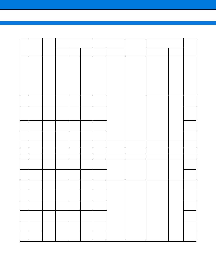
MB91230 Series
40
Note : P : Port selected, F : Specified function selected
(Continued)
Pin
no.
Pin
name
Port
name
Specified function
name
At initializing
At sleep
mode
At Stop mode
Re-
marks
Input
Output
Input/
Output
Function
name
Reset
initialization
HIZ
=
0
HIZ
=
1
31
P57/
INT15/
TIN0/
ADTG0
P57
INT15
TIN0
ADTG0
P57
Output
Hi-Z/
Input
enabled
Retention
of the
immediately
prior state
P :
Retention
of the
immediately
prior state
F :
Input
enabled
P :
Output
Hi-Z
F :
Input 0
enabled
32
PF3/
TOT3
PF3
TOT3
PF3
Retention
of the
immediately
prior state
Output
Hi-Z/
Input 0
fixed
33
PF4/
TIN3/
ADTG1
PF4
TIN3
ADTG1
PF4
34
PD0/
DA0
PD0
DA0
PD0
35
PD1/
DA1
PD1
DA1
PD1
36 AV
CC
37 AVRH
38 AV
SS
39
PC0/
AN0
PC0
AN0
PC0
Output
Hi-Z/
Input
enabled
Retention
of the
immediately
prior state
Retention
of the
immediately
prior state
Output
Hi-Z/
Input 0
fixed
40
PC1/
AN1
PC1
AN1
PC1
41
PC2/
AN2
PC2
AN2
PC2
Output
Hi-Z/
Input
enabled
Retention
of the
immediately
prior state
Retention
of the
immediately
prior state
Output
Hi-Z/
Input 0
fixed
42
PC3/
AN3
PC3
AN3
PC3
43
PC4/
AN4
PC4
AN4
PC4
44
PC5/
AN5
PC5
AN5
PC5
45
PC6/
AN6
PC6
AN6
PC6
46
PC7/
AN7
PC7
AN7
PC7
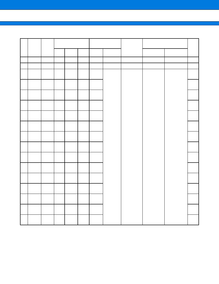
MB91230 Series
41
Note : P : Port selected, F : Specified function selected
(Continued)
Pin
no.
Pin
name
Port
name
Specified function
name
At initializing
At sleep
mode
At Stop mode
Re-
marks
Input
Output
Input/
Output
Function
name
Reset
initialization
HIZ
=
0
HIZ
=
1
47 V
SS
48 V
CC
3IO
49
P80/
SEG0
P80
SEG0
P80
Output
Hi-Z/
Input
enabled
Retention
of the
immediately
prior state
Retention
of the
immediately
prior state
P :
Output
Hi-Z/
Input 0
fixed
F :
Retention
of the
immediately
prior state
50
P81/
SEG1
P81
SEG1
P81
51
P82/
SEG2
P82
SEG2
P82
52
P83/
SEG3
P83
SEG3
P83
53
P84/
SEG4
P84
SEG4
P84
54
P85/
SEG5
P85
SEG5
P85
55
P86/
SEG6
P86
SEG6
P86
56
P87/
SEG7
P87
SEG7
P87
57
P90/
SEG8
P90
SEG8
P90
58
P91/
SEG9
P91
SEG9
P91
59
P92/
SEG10
P92
SEG10
P92
60
P93/
SEG11
P93
SEG11
P93
61
P94/
SEG12
P94
SEG12
P94
62
P95/
SEG13
P95
SEG13
P95
63
P96/
SEG14
P96
SEG14
P96
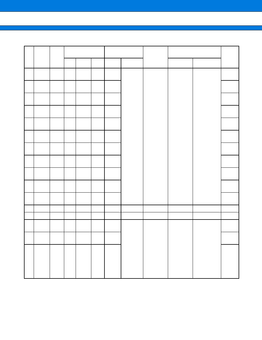
MB91230 Series
42
Note : P : Port selected, F : Specified function selected
(Continued)
Pin
no.
Pin
name
Port
name
Specified function
name
At initializing
At sleep
mode
At Stop mode
Re-
marks
Input
Output
Input/
Output
Function
name
Reset
initialization
HIZ
=
0
HIZ
=
1
64
P97/
SEG15
P97
SEG15
P97
Output
Hi-Z/
Input
enabled
Retention
of the
immediately
prior state
Retention
of the
immediately
prior state
P :
Output
Hi-Z/
Input 0 fixed
F :
Retention
of the
immediately
prior state
65
PA0/
SEG16
PA0
SEG16
PA0
66
PA1/
SEG17
PA1
SEG17
PA1
67
PA2/
SEG18
PA2
SEG18
PA2
68
PA3/
SEG19
PA3
SEG19
PA3
69
PA4/
SEG20
PA4
SEG20
PA4
70
PA5/
SEG21
PA5
SEG21
PA5
71
PA6/
SEG22
PA6
SEG22
PA6
72
PA7/
SEG23
PA7
SEG23
PA7
73
PB0/
SEG24
PB0
SEG24
PB0
74
PB1/
SEG25
PB1
SEG25
PB1
75 V
CC
76 V
SS
77
PB2/
SEG26
PB2
SEG26
PB2
Output
Hi-Z/
Input
enabled
Retention
of the
immediately
prior state
Retention
of the
immediately
prior state
P :
Output
Hi-Z/
Input 0
fixed
F :
Retention
of the
immediately
prior state
78
PB3/
SEG27
PB3
SEG27
PB3
79
P64/
SEG28
P64
SEG28
P64
open-
drain
pin,
I
OL
=
20 mA
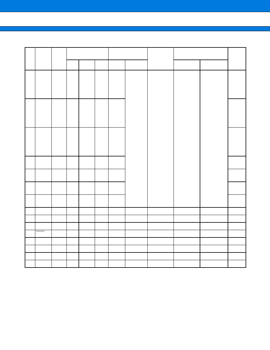
MB91230 Series
43
Note : P : Port selected, F : Specified function selected
(Continued)
Pin
no.
Pin
name
Port
name
Specified function
name
At initializing
At sleep
mode
At Stop mode
Re-
marks
Input
Output
Input/
Output
Function
name
Reset
initialization
HIZ
=
0
HIZ
=
1
80
P65/
SEG29
P65
SEG29
P65
Output
Hi-Z/
Input
enabled
Retention
of the
immediately
prior state
Retention
of the
immediately
prior state
P :
Output
Hi-Z/
Input 0 fixed
F :
Retention
of the
immediately
prior state
open-
drain
pin,
I
OL
=
20 mA
81
P66/
SEG30
P66
SEG30
P66
open-
drain
pin,
I
OL
=
20 mA
82
P67/
SEG31
P67
SEG31
P67
open-
drain
pin,
I
OL
=
20 mA
83
P70/
COM0
P70
COM0
P70
84
P71/
COM1
P71
COM1
P71
85
P72/
COM2
P72
COM2
P72
86
P73/
COM3
P73
COM3
P73
87 MOD2
88 MOD1
89 MOD0
90 INIT
91 V0
92 V1
93 V2
94 V3
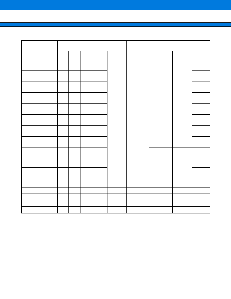
MB91230 Series
44
Note : P : Port selected, F : Specified function selected
(Continued)
Pin
no.
Pin
name
Port
name
Specified function
name
At initializing
At sleep
mode
At Stop mode
Remarks
Input
Output
Input/
Output
Function
name
Reset
initialization
HIZ
=
0
HIZ
=
1
95
P00/
SIN0
P00
SIN0
P00
Output
Hi-Z/
Input
enabled
Retention
of the
immediately
prior state
Retention
of the
immediately
prior state
Output
Hi-Z/
Input 0
fixed
96
P01/
SOT0
P01
SOT0
P01
97
P02/
SCK0
P02
SCK0 P02
98
P03/
SIN1
P03
SIN1
P03
99
P04/
SOT1
P04
SOT1
P04
100
P05/
SCK1
P05
SCK1 P05
101
P06/
IC0
P06
IC0
P06
102
P07/
IC1
P07
IC1
P07
103
P10/
INT0
P10
INT0
P10
P :
Retention
of the
immediately
prior state
F : Input
enabled
P : Output
Hi-Z
F : Input
enabled
Pull-up
options
can be
selected
104
P11/
INT1
P11
INT1
P11
Pull-up
options
can be
selected
105 V
CC
106 V
SS
107 X1
108 X0
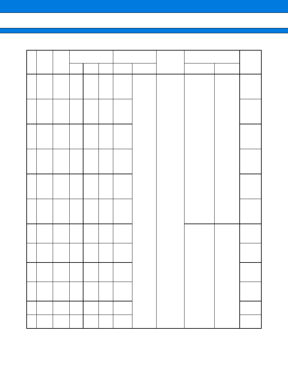
MB91230 Series
45
(Continued)
Note : P : Port selected, F : Specified function selected
Pin
no.
Pin
name
Port
name
Specified function
name
At initializing
At sleep
mode
At Stop mode
Remarks
Input
Output
Input/
Output
Function
name
Reset
initialization
HIZ
=
0
HIZ
=
1
109
P12/
INT2
P12
INT2
P12
Output
Hi-Z/
Input
enabled
Retention
of the
immediately
prior state
P :
Retention
of the
immediately
prior state
F :
Input
enabled
P :
Output
Hi-Z
F :
Input
enabled
Pull-up
options
can be
selected
110
P13/
INT3
P13
INT3
P13
Pull-up
options
can be
selected
111
P14/
INT4
P14
INT4
P14
Pull-up
options
can be
selected
112
P15/
INT5
P15
INT5
P15
Pull-up
options
can be
selected
113
P16/
INT6
P16
INT6
P16
Pull-up
options
can be
selected
114
P17/
INT7
P17
INT7
P17
Pull-up
options
can be
selected
115
P20/
CKI0/
OP0
P20
CKI0 OP0
P20
Retention
of the
immediately
prior state
Output
Hi-Z/
Input 0
fixed
116
P21/
CKI1/
OP1
P21
CKI1 OP1
P21
117
P22/
PWI0/
OP2
P22
PWI0 OP2
P22
118
P23/
PWI1/
OP3
P23
PWI1 OP3
P23
119
P24/
SIN2
P24
SIN2
P24
120
P25/
SOT2
P25
SOT2
P25
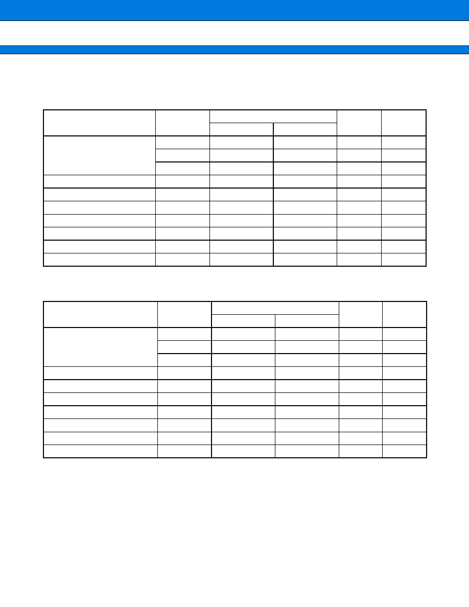
MB91230 Series
46
s
s
s
s
ELECTRICAL CHARACTERISTICS
1.
Absolute Maximum Ratings
MB91F233, MB91V230
* : This parameter is based on V
SS
=
AV
SS
=
0.0 V.
MB91F233L, MB91233L
* : This parameter is based on V
SS
=
AV
SS
=
0.0 V.
WARNING: Semiconductor devices can be permanently damaged by application of stress (voltage, current,
temperature, etc.) in excess of absolute maximum ratings. Do not exceed these ratings.
Parameter
Symbol
Rating
Unit
Remarks
Min
Max
Power supply voltage*
V
CC
V
SS
-
0.5
V
SS
+
6.0
V
V
CC
3
V
SS
-
0.5
V
SS
+
4.0
V
V
CC
3IO
V
SS
-
0.5
V
SS
+
4.0
V
Analog power supply voltage*
AV
CC
V
SS
-
0.5
V
SS
+
4.0
V
Input voltage*
VI
V
SS
-
0.5
V
CC
+
0.5
V
Input voltage* (open-drain)
VIND
V
SS
-
0.5
V
CC
+
0.5
V
Analog pin input voltage*
VIA
V
SS
-
0.5
AV
CC
+
0.5
V
Output voltage*
VO
V
SS
-
0.5
V
CC
+
0.5
V
Operating ambient temperature
Ta
-
40
+
85
∞
C
Storage temperature
Tstg
-
55
+
125
∞
C
Parameter
Symbol
Rating
Unit
Remarks
Min
Max
Power supply voltage*
V
CC
V
SS
-
0.5
V
SS
+
4.0
V
V
CC
3
V
SS
-
0.5
V
SS
+
4.0
V
V
CC
3IO
V
SS
-
0.5
V
SS
+
4.0
V
Analog power supply voltage*
AV
CC
V
SS
-
0.5
V
SS
+
4.0
V
Input voltage*
VI
V
SS
-
0.5
V
CC
+
0.5
V
Input voltage* (open-drain)
VIND
V
SS
-
0.5
V
CC
+
0.5
V
Analog pin input voltage*
VIA
V
SS
-
0.5
AV
CC
+
0.5
V
Output voltage*
VO
V
SS
-
0.5
V
CC
+
0.5
V
Operating ambient temperature
Ta
-
40
+
85
∞
C
Storage temperature
Tstg
-
55
+
125
∞
C
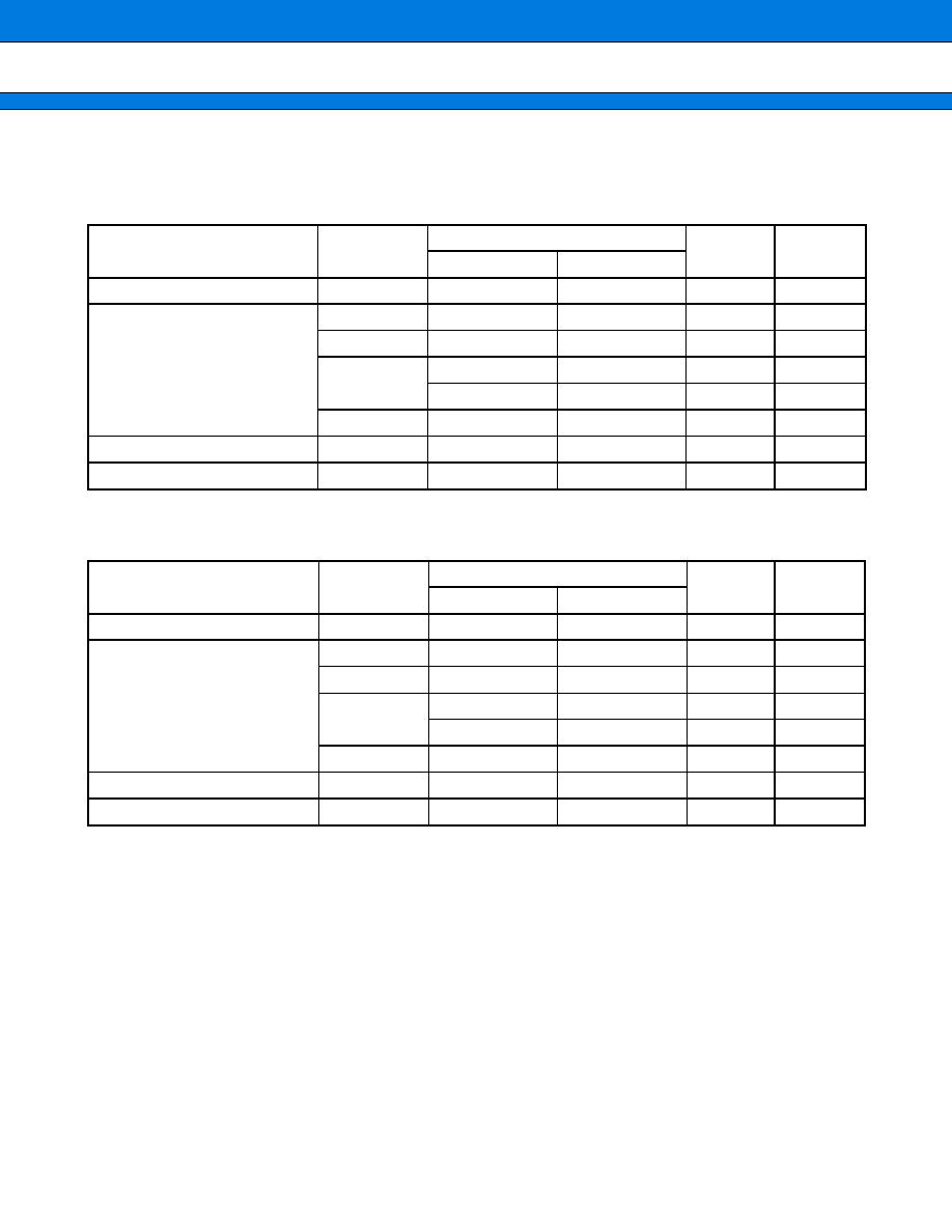
MB91230 Series
47
2.
Recommended Operating Conditions
MB91F233, MB91V230
(V
SS
=
AV
SS
=
0.0 V)
MB91F233L, MB91233L
(V
SS
=
AV
SS
=
0.0 V)
*1 : The standard power-supply voltage varies with the model of product.
*2 : Only for backup. Set V
CC
3
=
AV
CC
=
V
CC
3IO.
*3 : V3 must not exceed V
CC
.
*4 : For the relationships between V
CC
3 and operating frequencies, see section "4. AC Characteristics (4) Operation
Assurance Range".
For the MB91V230, please inquire separately.
Note : For normal use, set V
CC
3
=
V
CC
3B
=
AV
CC
=
V
CC
3IO.
WARNING: The recommended operating conditions are required in order to ensure the normal operation of the
semiconductor device. All of the device's electrical characteristics are warranted when the device is
operated within these ranges.
Always use semiconductor devices within their recommended operating condition ranges. Operation
outside these ranges may adversely affect reliability and could result in device failure.
No warranty is made with respect to uses, operating conditions, or combinations not represented on
the data sheet. Users considering application outside the listed conditions are advised to contact their
FUJITSU representatives beforehand.
Parameter
Symbol
Value
Unit
Remarks
Min
Max
Operating ambient temperature
Ta
-
40
+
85
∞
C
Power supply voltage
V
CC
4.00
5.25
V
*1
V
CC
3
3.00
3.60
V
*4
V
CC
3B
3.00
3.60
V
2.20
3.60
V
*2
V
CC
3IO
3.00
3.60
V
Analog power supply voltage
AV
CC
3.00
3.60
V
LCD reference voltage
V3
5.25
V
*3
Parameter
Symbol
Value
Unit
Remarks
Min
Max
Operating ambient temperature
Ta
-
40
+
85
∞
C
Power supply voltage
V
CC
3.00
3.60
V
*1
V
CC
3
3.00
3.60
V
*4
V
CC
3B
3.00
3.60
V
2.20
3.60
V
*2
V
CC
3IO
3.00
3.60
V
Analog power supply voltage
AV
CC
3.00
3.60
V
LCD reference voltage
V3
3.60
V
*3
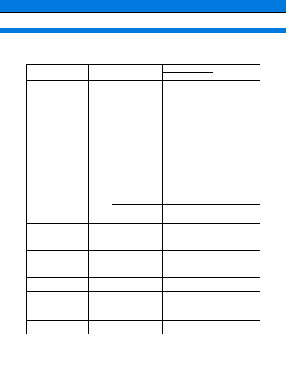
MB91230 Series
48
3.
DC Characteristics
MB91V230, MB91F233
(V
CC
=
4.0 V to 5.25 V, V
CC
3
=
V
CC
3B
=
V
CC
3IO
=
AV
CC
=
3.0 V to 3.6 V, V
SS
=
AV
SS
=
0.0 V, Ta
=
-
40
∞
C to
+
85
∞
C)
(Continued)
Parameter
Symbol Pin name
Conditions
Value
Unit
Remarks
Min
Typ
Max
Power supply
current
I
CC
V
CC
3
FLASH model normal
operation,
Ta
=
+
25
∞
C,
F
CP
=
33 MHz,
F
CPP
=
16.5 MHz
65
75
mA
FLASH model normal
operation,
Ta
=
+
25
∞
C,
F
CP
=
33 MHz,
F
CPP
=
33 MHz
73
83
mA
I
CCT
RTC mode,
@Ta
=
+
25
∞
C,
F
CP
=
32 kHz
20
50
µ
A
Watch timer,
RTC, LCDC
V
CC
3
=
V
CC
3B
=
2.4 V
I
CCH
STOP mode,
@Ta
=
+
25
∞
C,
F
CP
=
0 kHz
5
50
µ
A
I
CCS
SLEEP mode
F
CP
=
33 MHz,
F
CPP
=
16.5 MHz
21
25
mA
SLEEP mode
F
CP
=
33 MHz,
F
CPP
=
33 MHz
30
35
mA
"H" level input
voltage
V
IH
V
CC
◊
0.8
V
CC
V
X0A
V
CC
3B
=
2.2 V to 3.6 V
V
CC
3B
◊
0.8
V
CC
3B
V
When external
clock is used
"L" level input
voltage
V
IL
V
SS
V
CC
◊
0.2
V
X0A
V
CC
3B
=
2.2 V to 3.6 V
V
SS
V
SS
+
0.4
V
When external
clock is used
"H" level output
voltage
V
OH
I
OH
=
-
4 mA
V
CC
-
0.5
V
CC
V
"L" level output
voltage
V
OL
I
OL
=
4 mA
V
SS
0.4
V
P64 to 67 I
OL
=
20 mA
Input leakage
current
I
IL
-
5
5
µ
A
Open-drain output
leakage current
Ileak
-
10
10
µ
A
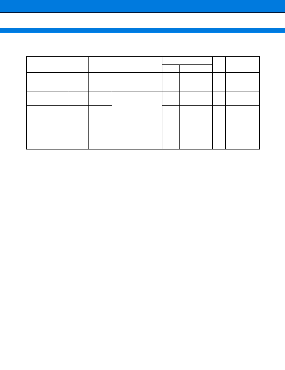
MB91230 Series
49
(Continued)
(V
CC
=
4.0 V to 5.25 V, V
CC
3
=
V
CC
3B
=
V
CC
3IO
=
AV
CC
=
3.0 V to 3.6 V, V
SS
=
AV
SS
=
0.0 V, Ta
=
-
40
∞
C to
+
85
∞
C)
Parameter
Symbol Pin name
Conditions
Value
Unit
Remarks
Min
Typ
Max
LCD division
resistance
R
LCD
V0 - V1,
V1 - V2,
V2 - V3
50
100
200
k
COM0 to COM3
output impedance
R
VCOM
COM0 to
COM3
V1 to V3
=
5.0 V
2.5
k
SEG00 to SEG31
output impedance
R
VSEG
SEG00 to
SEG31
15
k
LCDC leakage
current
I
LCDC
V0 to V3,
COM0 to
COM3,
SEG00 to
SEG31
-
5
5
µ
A
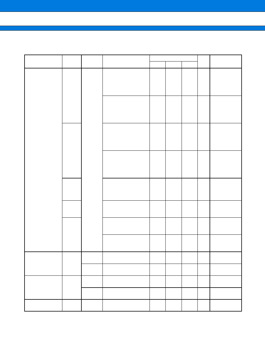
MB91230 Series
50
MB91F233L, MB91233L
(V
CC
=
V
CC
3
=
V
CC
3B
=
V
CC
3IO
=
AV
CC
=
3.0 V to 3.6 V, V
SS
=
AV
SS
=
0.0 V, Ta
=
-
40
∞
C to
+
85
∞
C)
(Continued)
Parameter
Symbol
Pin
name
Conditions
Value
Unit
Remarks
Min
Typ
Max
Power supply
current
I
CC
Vcc3
FLASH model normal
operation,
Ta
=
+
25
∞
C,
F
CP
=
33 MHz,
F
CPP
=
16.5 MHz
65
75
mA
FLASH model normal
operation,
Ta
=
+
25
∞
C,
F
CP
=
33 MHz,
F
CPP
=
33 MHz
73
83
mA
I
CC
ROM model normal
operation,
Ta
=
+
25
∞
C,
F
CP
=
33 MHz,
F
CPP
=
16.5 MHz
45
55
mA
ROM model normal
operation,
Ta
=
+
25
∞
C,
F
CP
=
33 MHz,
F
CPP
=
33 MHz
55
65
mA
I
CCT
RTC mode,
@Ta
=
+
25
∞
C,
F
CP
=
32 kHz
20
50
µ
A
Watch timer,
RTC, LCDC
V
CC
3
=
V
CC
3B
=
2.4 V
I
CCH
STOP mode,
@Ta
=
+
25
∞
C,
F
CP
=
0 MHz
5
50
µ
A
I
CCS
SLEEP mode
F
CP
=
33 MHz,
F
CPP
=
16.5 MHz
21
25
mA
SLEEP mode
F
CP
=
33 MHz,
F
CPP
=
33 MHz
30
35
mA
"H" level input
voltage
V
IH
V
CC
◊
0.8
V
CC
V
X0A
V
CC
3B
=
2.2 V to 3.6 V
V
CC
3B
◊
0.8
V
CC
3B
V
When external
clock is used
"L" level input
voltag
V
IL
V
SS
V
CC
◊
0.15
V
X0A
V
CC
3B
=
2.2 V to 3.6 V
V
SS
V
SS
+
0.4
V
When external
clock is used
"H" level output
voltage
V
OH
V
CC
=
3.3 V,
I
OH
=
-
2 mA
V
CC
-
0.5
V
CC
V
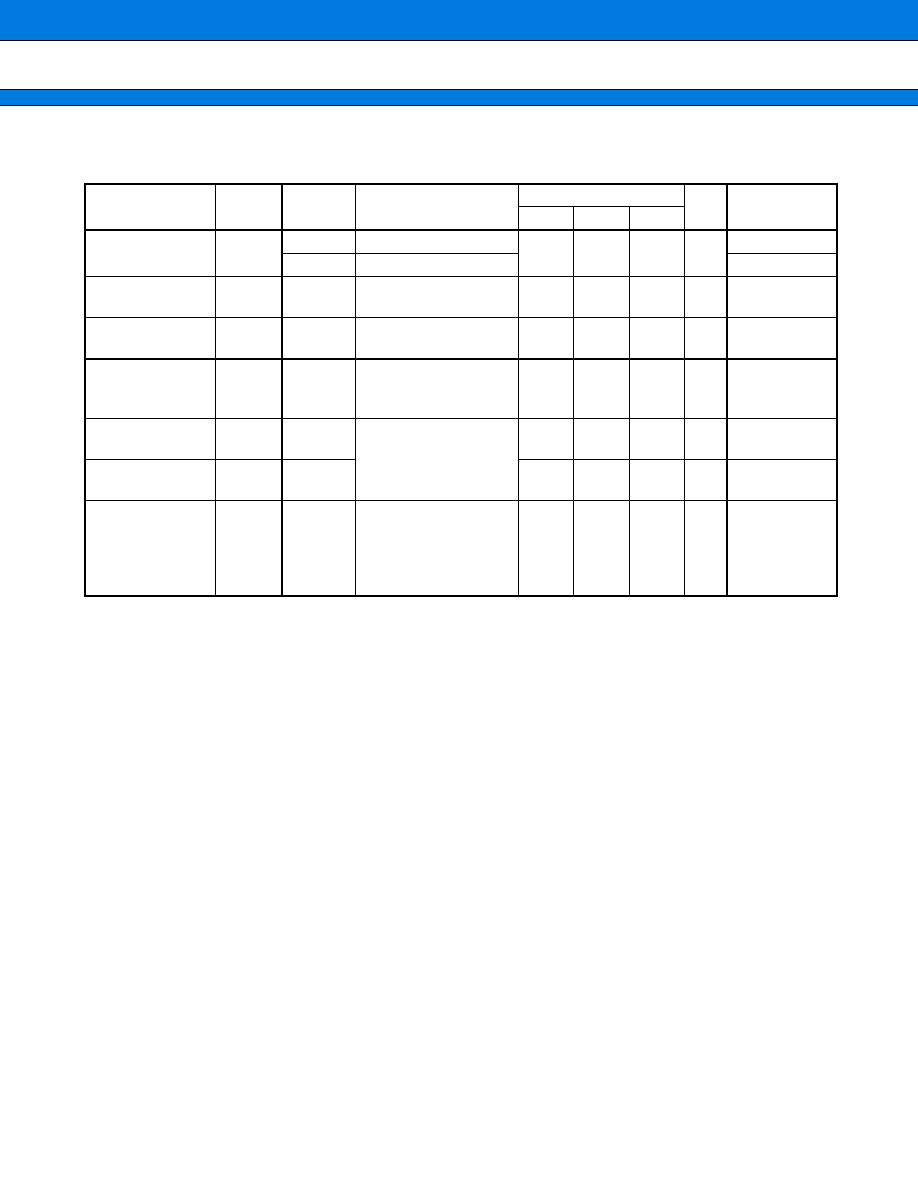
MB91230 Series
51
(Continued)
(V
CC
=
V
CC
3
=
V
CC
3B
=
V
CC
3IO
=
AV
CC
=
3.0 V to 3.6 V, V
SS
=
AV
SS
=
0.0 V, Ta
=
-
40
∞
C to
+
85
∞
C)
Parameter
Symbol
Pin
name
Conditions
Value
Unit
Remarks
Min
Typ
Max
"L" level output
voltage
V
OL
I
OL
=
2 mA
V
SS
0.4
V
P64 to 67 I
OL
=
10 mA
Input leakage
current
I
IL
-
5
5
µ
A
Open-drain output
leakage current
Ileak
-
10
10
µ
A
LCD division
resistance
R
LCD
V0 - V1,
V1 - V2,
V2 - V3
50
100
200
k
COM0 to COM3
output impedance
R
VCOM
COM0 to
COM3
V1 to V3
=
5.0 V
2.5
k
SEG00 to SEG31
output impedance
R
VSEG
SEG00 to
SEG31
15
k
LCDC leakage
current
I
LCDC
V0 to V3,
COM0 to
COM3,
SEG00 to
SEG31
-
5
-
5
µ
A
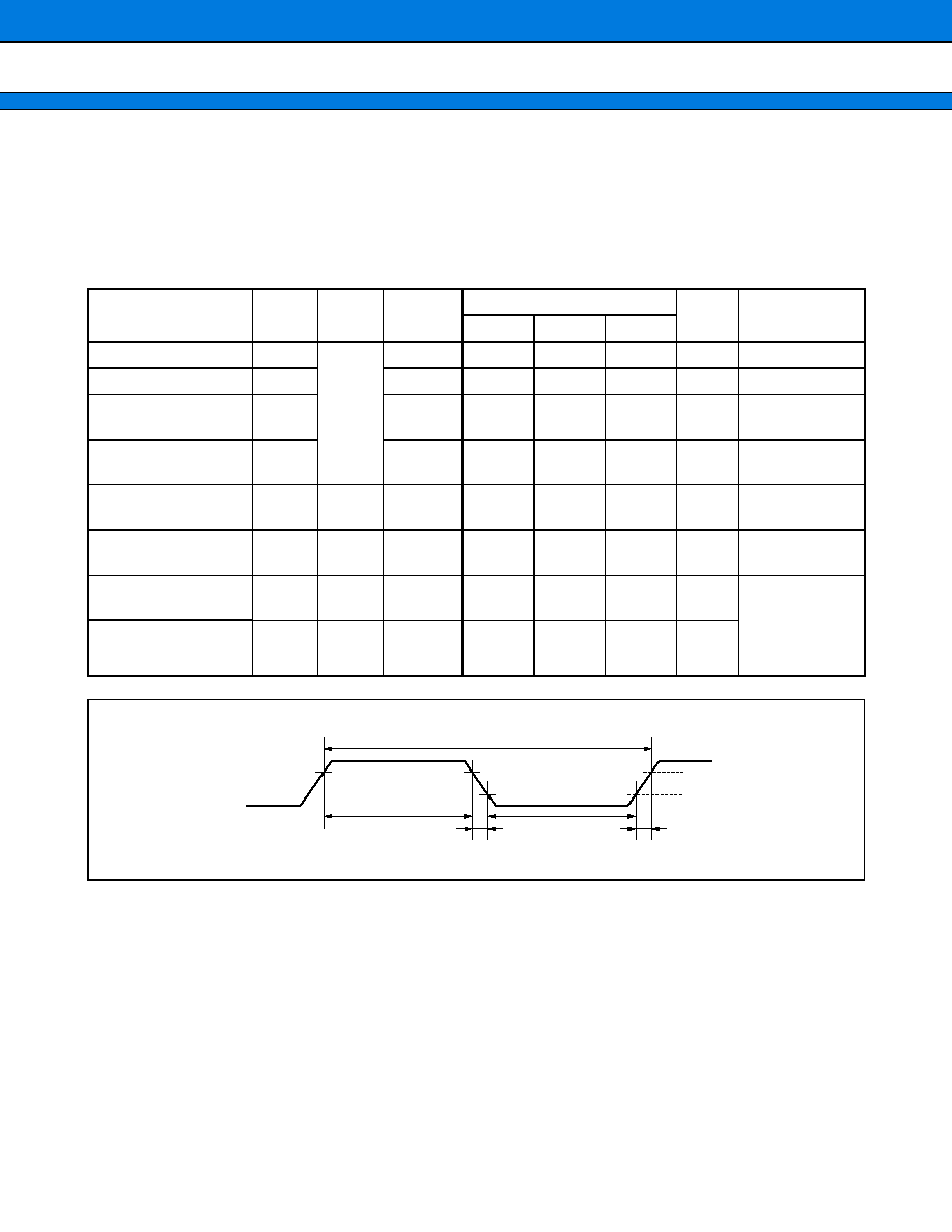
MB91230 Series
52
4.
AC Characteristics
(1) Main clock input standard
(MB91V230, MB91F233 : V
CC
=
4.0 V to 5.25 V, V
CC
3
=
V
CC
3B
=
V
CC
3IO
=
AV
CC
=
3.0 V to 3.6 V, V
SS
=
AV
SS
=
0.0 V,
Ta
=
-
40
∞
C to
+
85
∞
C)
(MB91F233L, MB91233L : V
CC
=
V
CC
3
=
V
CC
3B
=
V
CC
3IO
=
AV
CC
=
3.0 V to 3.6 V, V
SS
=
AV
SS
=
0.0 V,
Ta
=
-
40
∞
C to
+
85
∞
C)
Parameter
Sym-
bol
Pin
name
Condi-
tions
Value
Unit
Remarks
Min
Typ
Max
Input frequency
F
C
X0
3.6
4
4.2
MHz
Input clock cycle
t
CYL
250
ns
Input clock pulse width
P
WH
/t
CYL
P
WL
/t
CYL
40
60
%
Input clock rise time
and fall time
t
CR
t
CF
5
ns
At external clock
Internal operating
clock frequency
F
CP
33.6
MHz
Internal operating
clock cycle time
t
CP
29.7
ns
Peripheral clock
frequency
F
CPP
33.6
MHz
Peripheral clock
is derived from
internal operat-
ing clock divided
by 1/1 to 1/16.
Peripheral clock cycle
time
t
CYCP
29.7
ns
X0
0.8
◊
V
CC
3
0.8
◊
V
CC
3
V
SS
+
0.4
V
SS
+
0.4
0.8
◊
V
CC
3
t
CYL
P
WH
P
WL
t
CF
t
CR
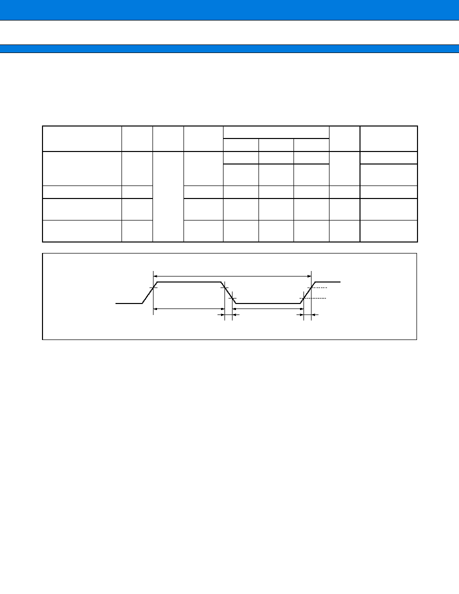
MB91230 Series
53
(2) Subclock input standard
(MB91V230, MB91F233 : V
CC
=
4.0 V to 5.25 V, V
CC
3
=
V
CC
3B
=
V
CC
3IO
=
AV
CC
=
3.0 V to 3.6 V, V
SS
=
AV
SS
=
0.0 V,
Ta
=
-
40
∞
C to
+
85
∞
C)
(MB91F233L, MB91233L : V
CC
=
V
CC
3
=
V
CC
3B
=
V
CC
3IO
=
AV
CC
=
3.0 V to 3.6 V, V
SS
=
AV
SS
=
0.0 V,
Ta
=
-
40
∞
C to
+
85
∞
C)
Parameter
Sym-
bol
Pin
name
Condi-
tions
Value
Unit
Remarks
Min
Typ
Max
Input frequency
F
CL
X0A
32.768
kHz
28.571
32.768
35.714
At external
clock
Input clock cycle
t
LCYL
28.0
35.0
µ
s
Input clock pulse width
P
WLH
/t
LCYL
P
WLL
/t
LCYL
45
55
%
Input clock rise time
and fall time
t
CR
/t
LCYL
t
CF
/t
LCYL
5
%
At external
clock
X0A
0.8
◊
V
CC
3B
0.8
◊
V
CC
3B
V
SS
+
0.4
V
SS
+
0.4
0.8
◊
V
CC
3B
t
LCYL
P
WLH
P
WLL
t
CF
t
CR
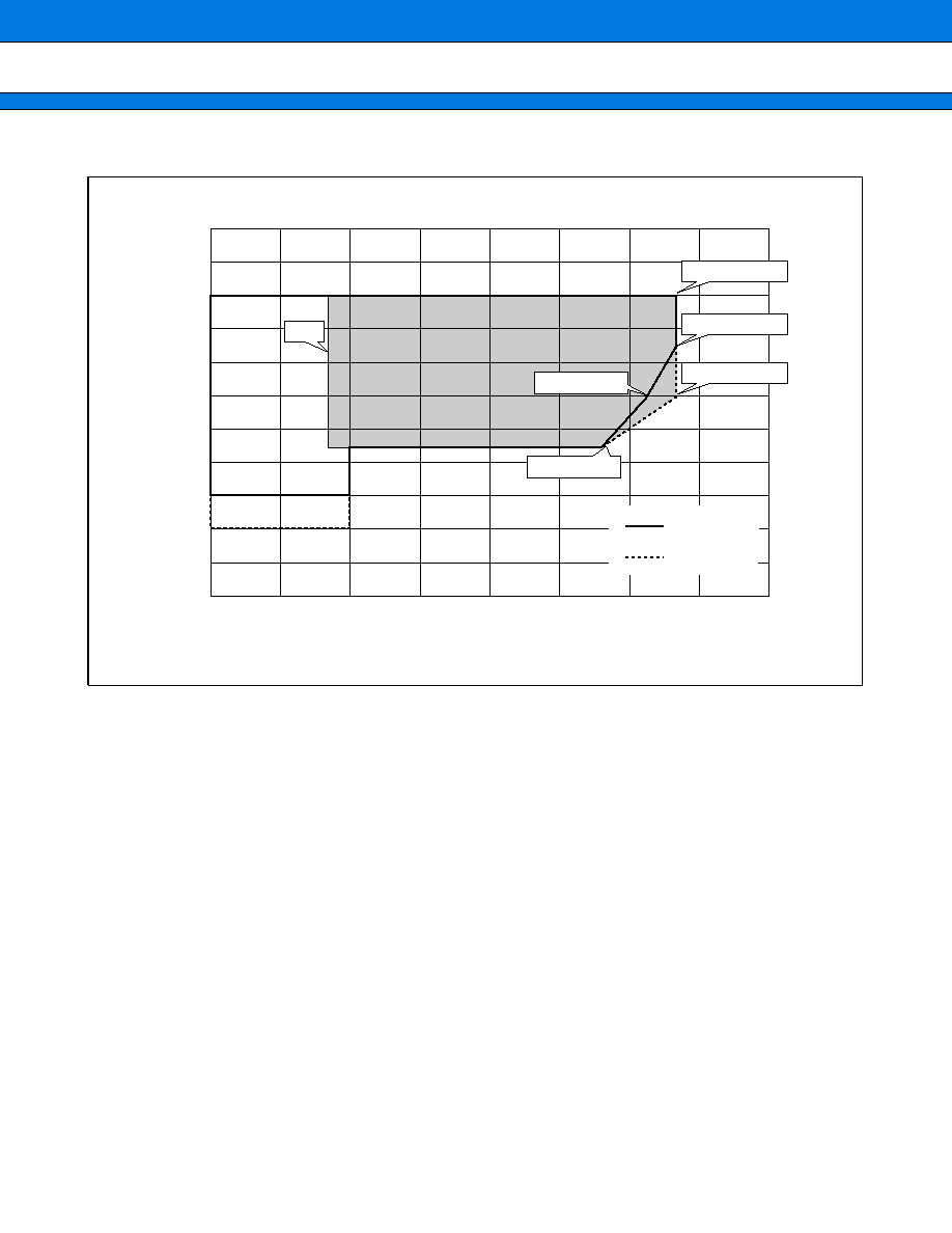
MB91230 Series
54
(3) Operation Assurance Range
4.0
3.8
3.6
3.4
3.2
3.0
2.8
2.6
2.4
2.2
2.0
1.8
32 kHz
5
10
15
20
25
30
35
40
MB91F233
MB91F233L
MB91233L
PLL OFF
8 MHz
PLL ON
32 MHz@ 3.0 V
28 MHz@ 2.7 V
33.6 MHz@ 3.0 V
33.6 MHz@ 3.3 V
33.6 MHz@ 3.6 V
Internal power supply voltage V
CC
3 [V]
Internal operation frequency [MHz]
MB91230 Series
55
(4) PLL oscillation stabilization time (LOCK UP time)
(MB91V230, MB91F233 : V
CC
=
4.0 V to 5.25 V, V
CC
3
=
V
CC
3B
=
V
CC
3IO
=
AV
CC
=
3.0 V to 3.6 V, V
SS
=
AV
SS
=
0.0 V,
Ta
=
-
40
∞
C to
+
85
∞
C)
(MB91F233L, MB91233L : V
CC
=
V
CC
3
=
V
CC
3B
=
V
CC
3IO
=
AV
CC
=
3.0 V to 3.6 V, V
SS
=
AV
SS
=
0.0 V,
Ta
=
-
40
∞
C to
+
85
∞
C)
(5) Reset input standards
(MB91V230, MB91F233 : V
CC
=
4.0 V to 5.25 V, V
CC
3
=
V
CC
3B
=
V
CC
3IO
=
AV
CC
=
3.0 V to 3.6 V, V
SS
=
AV
SS
=
0.0 V,
Ta
=
-
40
∞
C to
+
85
∞
C)
(MB91F233L, MB91233L : V
CC
=
V
CC
3
=
V
CC
3B
=
V
CC
3IO
=
AV
CC
=
3.0 V to 3.6 V, V
SS
=
AV
SS
=
0.0 V,
Ta
=
-
40
∞
C to
+
85
∞
C)
*1 : When turning the power on, keep INIT input until the oscillation circuit provides stable oscillation.
*2 : t
CP
indicates cycle time of CPU operating clock.
Parameter
Symbol
value
Unit
Remarks
Min
Max
PLL oscillation stabilization
(LOCK UP time)
t
LOCK
500
µ
s
Time from when the PLL
starts operating to when its
oscillation becomes stable
Parameter
Symbol
Pin
name
Condi-
tions
Value
Unit
Remarks
Min
Max
Reset input time
(at power-on)
t
INITX
INIT
ns
*1
Reset input time
(other than at power-on)
t
CP
◊
10
ns
*2
V
IL
V
IL
t
INITX
INIT
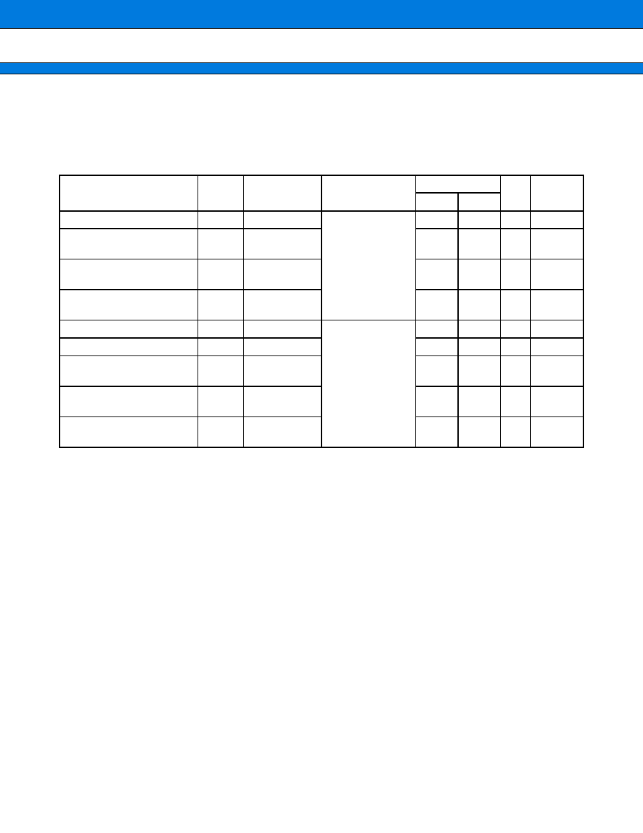
MB91230 Series
56
(6)UART timing
(MB91V230, MB91F233 : V
CC
=
4.0 V to 5.25 V, V
CC
3
=
V
CC
3B
=
V
CC
3IO
=
AV
CC
=
3.0 V to 3.6 V, V
SS
=
AV
SS
=
0.0 V,
Ta
=
-
40
∞
C to
+
85
∞
C)
(MB91F233L, MB91233L : V
CC
=
V
CC
3
=
V
CC
3B
=
V
CC
3IO
=
AV
CC
=
3.0 V to 3.6 V, V
SS
=
AV
SS
=
0.0 V,
Ta
=
-
40
∞
C to
+
85
∞
C)
* : t
CYCP
represents the cycle time of peripheral operating clock.
Note : This specification applies to clock synchronous mode operation.
Parameter
Symbol
Pin name
Conditions
Value
Unit Remarks
Min
Max
Serial clock cycle time
t
SCYC
SCK0 to SCK2
Internal shift clock
operation
8 t
CYCP
*
ns
SCK
SOT delay time
t
SLOV
SCK0 to SCK2,
SOT0 to SOT2
-
80
80
ns
Valid SIN
SCK
t
IVSH
SCK0 to SCK2,
SIN0 to SIN2
100
ns
SCK
Valid SIN hold time
t
SHIX
SCK0 to SCK2,
SIN0 to SIN2
60
ns
Serial clock "H" pulse width
t
SHSL
SCK0 to SCK2
External shift clock
operation
4 t
CYCP
*
ns
Serial clock "L" pulse width
t
SLSH
SCK0 to SCK2
4 t
CYCP
*
ns
SCK
SOT delay time
t
SLOV
SCK0 to SCK2,
SOT0 to SOT2
150
ns
Valid SIN
SCK
t
IVSH
SCK0 to SCK2,
SIN0 to SIN2
60
ns
SCK
Valid SIN hold time
t
SHIX
SCK0 to SCK2,
SIN0 to SIN2
60
ns
MB91230 Series
57
∑
Internal shift clock mode
SCK0 to SCK2
SOT0 to SOT2
SIN0 to SIN2
t
SCYC
t
SLOV
t
IVSH
t
SHIX
V
OL
V
OL
V
OH
V
OH
V
OL
V
OH
V
OL
V
OH
V
OL
∑
External shift clock mode
SCK0 to SCK2
SOT0 to SOT2
SIN0 to SIN2
t
SLSH
t
SHSL
t
SLOV
t
IVSH
t
SHIX
V
OL
V
OL
V
OH
V
OH
V
OH
V
OL
V
OH
V
OL
V
OH
V
OL
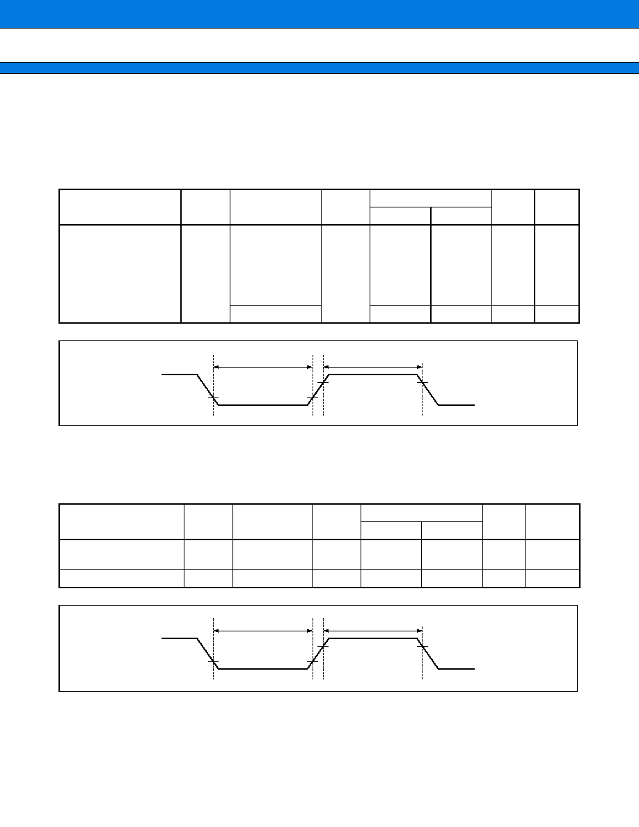
MB91230 Series
58
(7) Free-run timer clock, Reload timer event input, Up/down counter input, Input capture input,
Interrupt input timing
(MB91V230, MB91F233 : V
CC
=
4.0 V to 5.25 V, V
CC
3
=
V
CC
3B
=
V
CC
3IO
=
AV
CC
=
3.0 V to 3.6 V, V
SS
=
AV
SS
=
0.0 V,
Ta
=
-
40
∞
C to
+
85
∞
C)
(MB91F233L, MB91233L : V
CC
=
V
CC
3
=
V
CC
3B
=
V
CC
3IO
=
AV
CC
=
3.0 V to 3.6 V, V
SS
=
AV
SS
=
0.0 V,
Ta
=
-
40
∞
C to
+
85
∞
C)
* : t
CYCP
indicates peripheral clock cycle time.
(8) A/D trigger, PWI (PWC) input timing
(MB91V230, MB91F233 : V
CC
=
4.0 V to 5.25 V, V
CC
3
=
V
CC
3B
=
V
CC
3IO
=
AV
CC
=
3.0 V to 3.6 V, V
SS
=
AV
SS
=
0.0 V,
Ta
=
-
40
∞
C to
+
85
∞
C)
(MB91F233L, MB91233L : V
CC
=
V
CC
3
=
V
CC
3B
=
V
CC
3IO
=
AV
CC
=
3.0 V to 3.6 V, V
SS
=
AV
SS
=
0.0 V,
Ta
=
-
40
∞
C to
+
85
∞
C)
* : t
CYCP
indicates peripheral clock cycle time.
Parameter
Symbol
Pin name
Condi-
tions
Value
Unit
Re-
marks
Min
Max
Input pulth width
t
TIWH
t
TIWL
CKI0, CKI1
TIN0, TIN1, TIN2
IC0, IC1
AIN0, AIN1
BIN0, BIN1
ZIN0, ZIN1
t
CYCP
◊
2
ns
*
INT0 to INT15
t
CYCP
◊
3
ns
*
Parameter
Symbol
Pin name
Condi-
tions
Value
Unit
Remarks
Min
Max
A/D trigger input (falling)
t
TADTG
ADTG0
ADTG1
t
CYCP
◊
2
ns
*
PWI (PWC) input (rising)
t
PWI
PWI0, PWI1
t
CYCP
◊
2
ns
*
V
IH
V
IH
V
IL
V
IL
t
TIWH
t
TIWL
V
IH
V
IH
V
IL
V
IL
t
TADTG
t
TPWI
MB91230 Series
59
5.
Electrical Characteristics for the A/D Converter
(V
CC
3IO
=
AV
CC
=
3.0 V to 3.6 V, V
SS
=
AV
SS
=
0.0 V, AVRH
=
3.0 V to 3.6 V, Ta
=
0
∞
C to
+
85
∞
C)
*1 : Measured in the CPU sleep state
*2 : It depends on the clock cycle supplied to peripheral resources.
*3 : AVRL pin is only for FLGA package product. AVRL pin is connected to AV
SS
inside the IC on QFP package
product.
*4 : The current when the CPU is in stop mode and the A/D converter is not operaring.
Parameter
Value
Unit
Remarks
Min
Typ
Max
Resolution
10
bit
AV
CC
=
3.3 V,
At AVRH
=
3.3 V
At CPU sleep mode
Total error*
1
-
5.0
+
5.0
LSB
Nonlinear error*
1
-
3.5
+
3.5
LSB
Differential linear error*
1
-
2.5
+
2.5
LSB
Zero transition voltage*
1
-
2.0
+
1.0
+
6.0
LSB
Full transition voltage*
1
AVRH
-
5.5
AVRH
-
1.0
AVRH
+
3.0
LSB
Conversion time
1.69*
2
µ
s
Power supply voltage
(analog
+
digital)
3.6
mA
5
µ
A
Reference power supply current
(between AVRH and AVRL)
470
µ
A
AVRH
=
3.0 V,
At AVRL
=
0.0 V*
3
10
µ
A
At power-down*
4
Analog input capacitance
40
pF
Inter-channel disparity
4
LSB
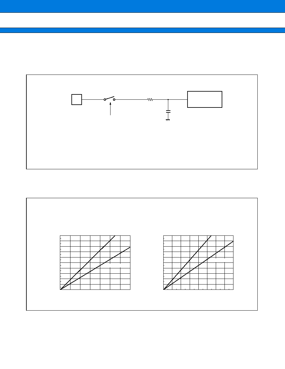
MB91230 Series
60
∑
∑
∑
∑
About the external impedance of the analog input and its sampling time
∑
A/D converter with sample and hold circuit. If the external impedance is too high to keep sufficient sampling
time, the analog voltage charged to the internal sampling and hold capacitor is insufficient, adversely affecting
A/D conversion precision.
∑
To satisfy the A/D conversion precision standard, consider the relationship between the external impedance
and minimum sampling time and either adjust the resistor value and operating frequency or decrease the
external impedance so that the sampling time is longer than the minimum value.
∑
If the sampling time cannot be sufficient, connect a capacitor of about 0.1
µ
F to the analog input pin.
∑
About errors
As |AVRH
-
AV
SS
| becomes smaller, values of relative errors grow larger.
∑
∑
∑
∑
Analog input circuit model
R
C
Comparator
During sampling : ON
Analog input
Note : The values are reference values.
R
C
MB91233L
0.18 k
(Max)
63.0 pF (Max)
MB91F233
0.18 k
(Max)
39.0 pF (Max)
MB91F233L
0.18 k
(Max)
39.0 pF (Max)
100
90
80
70
60
50
40
30
20
10
0
0
5
10
15
20
25
30
35
MB91F233
MB91F233L
MB91233L
(External impedance
=
0 k
to 100 k
)
Minimum sampling time (
µ
s)
External impedance (k
)
20
18
16
14
12
10
8
6
4
2
0
0
1
2
3
4
5
6
8
7
MB91F233
MB91F233L
MB91233L
(External impedance
=
0 k
to 20 k
)
Minimum sampling time (
µ
s)
External impedance (k
)
∑
∑
∑
∑
The relationship between the external impedance and minimum sampling time
MB91230 Series
61
6.
Electrical Characteristics for the D/A Converter
(V
CC
3IO
=
AV
CC
=
3.0 V to 3.6 V, V
SS
=
AV
SS
=
0.0 V, Ta
=
0
∞
C to
+
85
∞
C)
* : The current consumption by this D/A converter varies with input digital code.
This standard value indicates the current consumed when the digital code that maximizes the current consumption
is input.
7.
Flash Memory Write/Erase Characteristics
* : This value comes from the technology qualification (using Arrhenius equation to translate high temperature
measurements into normalized value at
+
85
∞
C).
Parameter
Value
Unit
Remarks
Min
Typ
Max
Resolution
8
bit
Nonlinear error
-
2.0
+
2.0
LSB
When the output is unloaded
Differential linear error
-
1.0
+
1.0
LSB
When the output is unloaded
Conversion speed
0.6
µ
s
When load capacitance
(C
L
) = 20 pF
3.0
µ
s
When load capacitance
(C
L
) = 100 pF
Output impedance
2.0
2.9
3.8
k
Analog current
40
µ
A
10
µ
s conversion, when the
output is unloaded
460*
µ
A
When the input digital code is
fixed at 7A
H
or 85
H
0.1
µ
A
At power-down
Parameter
Conditions
Value
Unit
Remarks
Min
Typ
Max
Sector erase time
Ta
=
+
25
∞
C,
Vcc
=
5.0 V
1
15
s
Excludes 00
H
programming
prior erasure
Chip erase time
Ta
=
+
25
∞
C,
Vcc
=
5.0 V
10
s
Excludes 00
H
programming
prior erasure
Byte write time
Ta
=
+
25
∞
C,
Vcc
=
5.0 V
8
3,600
µ
s
Not including system-level
overhead time.
Chip write time
Ta
=
+
25
∞
C,
Vcc
=
5.0 V
2.1
s
Not including system-level
overhead time.
Erase/write cycle
10,000
cycle
Flash data retention time Average Ta
=
+
85
∞
C
20
year
*
MB91230 Series
62
s
s
s
s
ORDERING INFORMATION
Part number
Package
Remarks
MB91V230CR-ES
401-pin ceramic PGA
(PGA-401C-A02)
MB91F233PFF-GE1
120-pin plastic LQFP
(FPT-120P-M05)
MB91F233LPFF-GE1
120-pin plastic LQFP
(FPT-120P-M05)
MB91F233LLGA-GE1
128-pin plastic FLGA
(LGA-128P-M01)
MB91233LPFF-G-xxx-BNDE1
120-pin plastic LQFP
(FPT-120P-M05)
MB91233LLGA-Gxxx-BNDE1
128-pin plastic FLGA
(LGA-128P-M01)
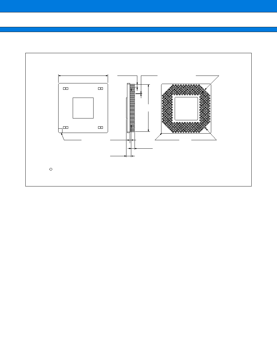
MB91230 Series
63
s
s
s
s
PACKAGE DIMENSIONS
(Continued)
401-pin Ceramic PGA
(PGA-401C-A02)
Dimensions in mm (inches) .
Note : The values in parentheses are reference values.
48.26 ± 0.55
(1.900 ± .022)
SQ
INDEX AREA
1994 FUJITSU LIMITED R401002SC-2-2
2.54 (.100) TYP
0.40 ± 0.10
(.016 ± .004)
DIA
45.72 (1.800)
REF
1.20 ± 0.25
(.047 ± .010)
5.27 (.207)
MAX
3.40 ± 0.40
(.134 ± .016)
1.00 (.039) DIA TYP
(4 PLCS)
EXTRA INDEX PIN
1.02 (.040) C TYP
(4 PLCS)
C
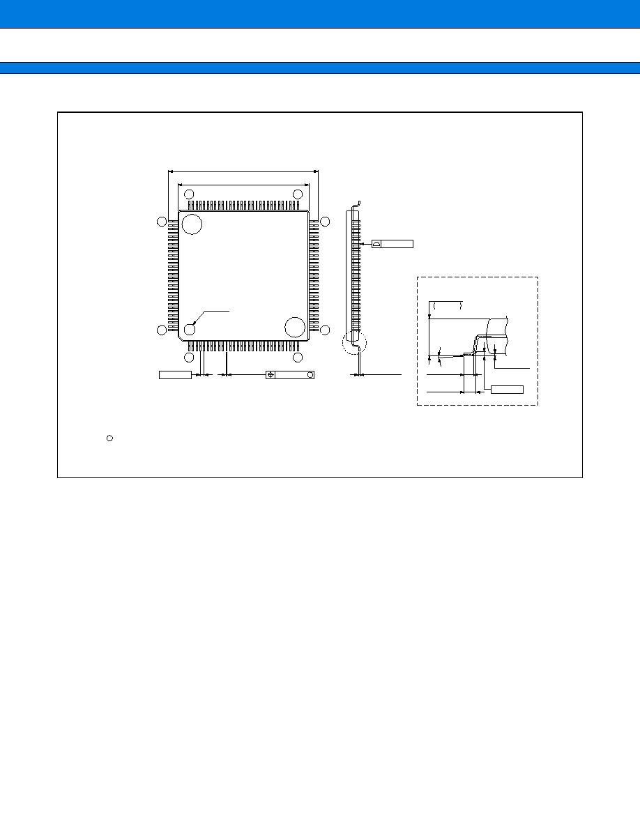
MB91230 Series
64
(Continued)
120-pin Plastic LQFP
(FPT-120P-M05)
Note 1) * : These dimensions do not include resin protrusion.
Note 2) Pins width and pins thickness include plating thickness.
Note 3) Pins width do not include tie bar cutting remainder.
Dimensions in mm (inches) .
Note : The values in parentheses are reference values.
C
2003 FUJITSU LIMITED F120006S-c-4-5
0.07(.003)
M
INDEX
16.00±0.20(.630±.008)SQ
14.00±0.10(.551±.004)SQ
1
30
31
60
91
120
61
90
LEAD No.
(Stand off)
0.10±0.10
(.004±.004)
0.25(.010)
(.024±.006)
0.60±0.15
(.020±.008)
0.50±0.20
(Mounting height)
0~8
∞
Details of "A" part
1.50
+0.20
≠0.10
+.008
≠.004
.059
"A"
0.40(.016)
0.16±0.03
(.006±.001)
0.145±0.055
(.006±.002)
0.08(.003)
*
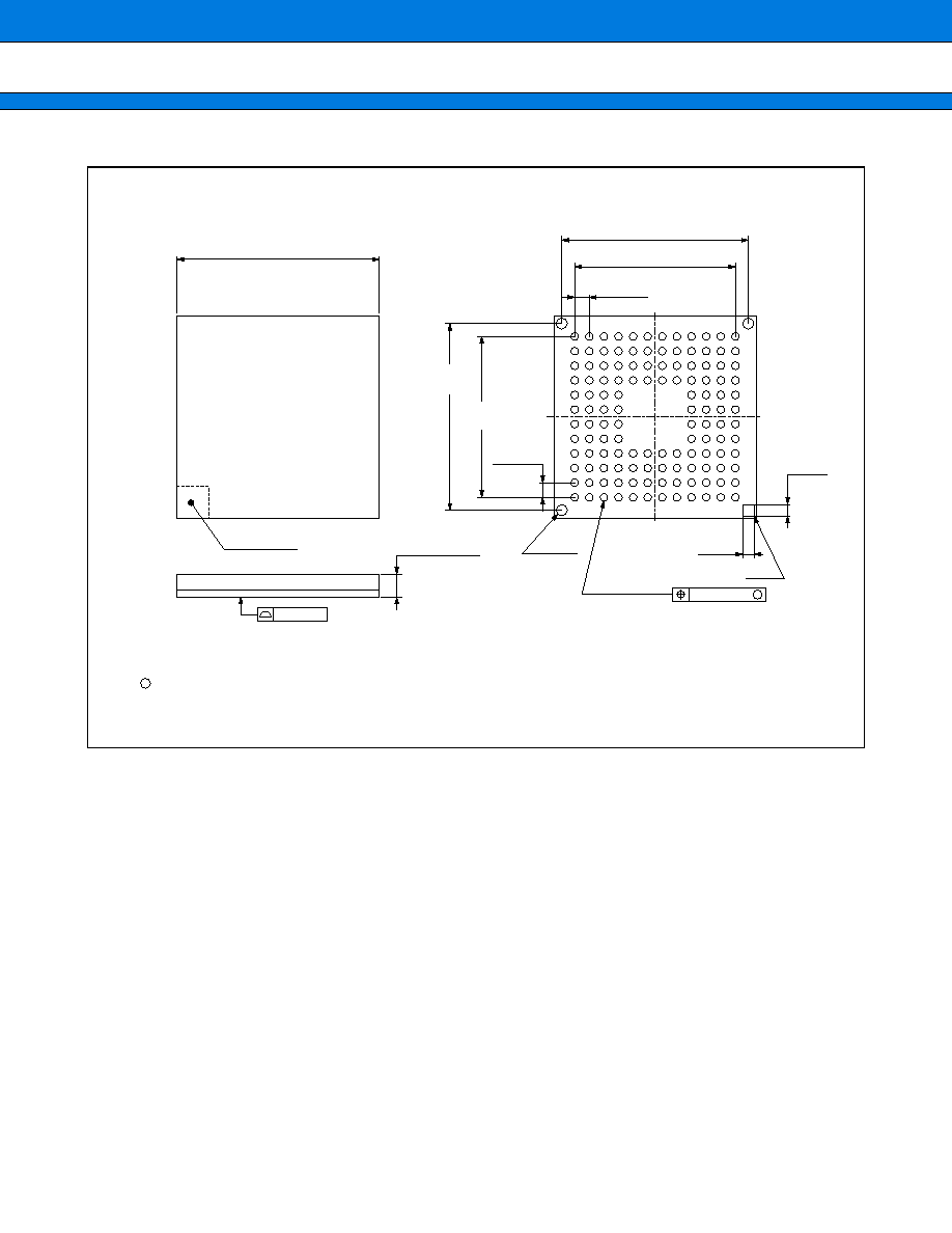
MB91230 Series
65
(Continued)
128-pin plastic FLGA
(LGA-128P-M01)
Dimensions in mm (inches) .
Note : The values in parentheses are reference values.
C
2004 FUJITSU LIMITED L128001S-c-1-1
9.00±0.10(.354±.004)SQ
1.00(.040)MAX
(Seated Height)
1
A
(128-¯.014±.002)
128-¯0.35±0.05
INDEX AREA
0.65(.026)
TYP
M
¯
0.08(¯.003)
0.08(.003)
2
3
4
5
6
7
8
9
10
11
12
B
C
D
E
F
G
H
J
K
L
M
Index
3-¯0.50
(3-¯.020)
7.15(.282)
REF
8.30(.327)
REF
7.15(.282)
REF
8.30(.327)
REF
TYP
0.65(.026)
(0.50)
((.020))
((.020))
(0.50)

MB91230 Series
FUJITSU LIMITED
All Rights Reserved.
The contents of this document are subject to change without notice.
Customers are advised to consult with FUJITSU sales
representatives before ordering.
The information, such as descriptions of function and application
circuit examples, in this document are presented solely for the
purpose of reference to show examples of operations and uses of
Fujitsu semiconductor device; Fujitsu does not warrant proper
operation of the device with respect to use based on such
information. When you develop equipment incorporating the
device based on such information, you must assume any
responsibility arising out of such use of the information. Fujitsu
assumes no liability for any damages whatsoever arising out of
the use of the information.
Any information in this document, including descriptions of
function and schematic diagrams, shall not be construed as license
of the use or exercise of any intellectual property right, such as
patent right or copyright, or any other right of Fujitsu or any third
party or does Fujitsu warrant non-infringement of any third-party's
intellectual property right or other right by using such information.
Fujitsu assumes no liability for any infringement of the intellectual
property rights or other rights of third parties which would result
from the use of information contained herein.
The products described in this document are designed, developed
and manufactured as contemplated for general use, including
without limitation, ordinary industrial use, general office use,
personal use, and household use, but are not designed, developed
and manufactured as contemplated (1) for use accompanying fatal
risks or dangers that, unless extremely high safety is secured, could
have a serious effect to the public, and could lead directly to death,
personal injury, severe physical damage or other loss (i.e., nuclear
reaction control in nuclear facility, aircraft flight control, air traffic
control, mass transport control, medical life support system, missile
launch control in weapon system), or (2) for use requiring
extremely high reliability (i.e., submersible repeater and artificial
satellite).
Please note that Fujitsu will not be liable against you and/or any
third party for any claims or damages arising in connection with
above-mentioned uses of the products.
Any semiconductor devices have an inherent chance of failure. You
must protect against injury, damage or loss from such failures by
incorporating safety design measures into your facility and
equipment such as redundancy, fire protection, and prevention of
over-current levels and other abnormal operating conditions.
If any products described in this document represent goods or
technologies subject to certain restrictions on export under the
Foreign Exchange and Foreign Trade Law of Japan, the prior
authorization by Japanese government will be required for export
of those products from Japan.
F0410
©
2004 FUJITSU LIMITED Printed in Japan