DS07-16507-1E
FUJITSU SEMICONDUCTOR
DATA SHEET
32
-
bit Proprietary Microcontroller
CMOS
FR60Lite
MB91260B Series
MB91263B/MB91F264B
s
s
s
s
DESCRIPTION
The MB91260B series is a 32-bit RISC microcontroller designed by Fujitsu for embedded control applications
which require high-speed processing.
The CPU is used the FR family and the compatibility of FR60Lite.
s
s
s
s
FEATURES
∑
FR60Lite CPU
∑ 32-bit RISC, load/store architecture with a five-stage pipeline
∑ Maximum operating frequency : 33 MHz (oscillation frequency 4.192 MHz, oscillation frequency 8-multiplier
(PLL clock multiplication method)
∑ 16-bit fixed length instructions (basic instructions)
∑ Execution speed of instructions : 1 instruction per cycle
∑ Memory-to-memory transfer, bit handling, barrel shift instructions, etc : Instructions suitable for embedded
applications
∑ Function entry/exit instructions, multiple-register load/store instructions : Instructions adapted for C-language
(Continued)
s
s
s
s
PACKAGES
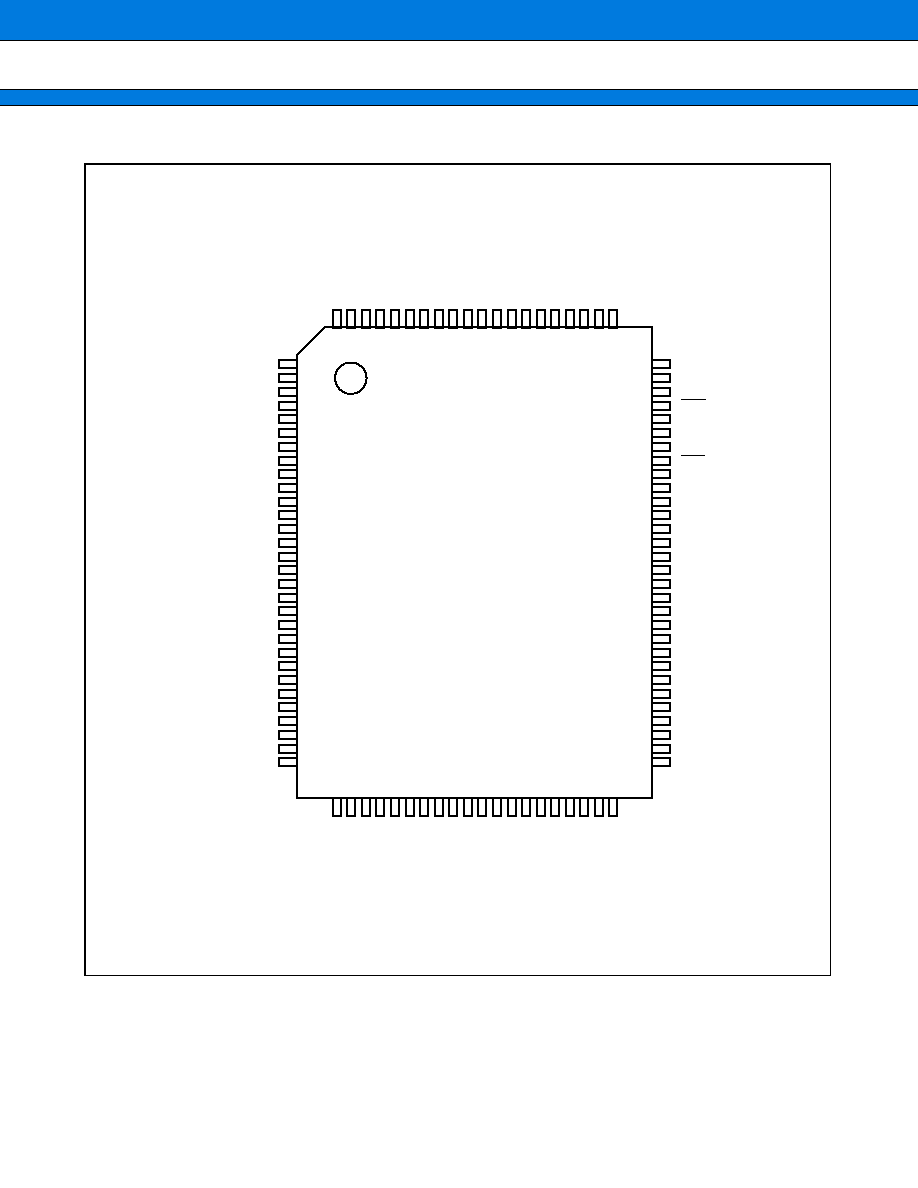
100-pin plastic QFP
100-pin plastic LQFP
(FTP-100P-M06)
(FTP-100P-M05)

MB91260B Series
2
(Continued)
∑ Register interlock function : Facilitates coding in assembler.
∑ Built-in multiplier with instruction-level support
∑
32 bit multiplication with sign : 5 cycles
∑
16 bit multiplication with sign : 3 cycles
∑ Interrupt (PC, PS save) : 6 cycles, 16 priority levels
∑ Harvard architecture allowing program access and data access to be executed simultaneously
∑ FR family instruction compatible
∑
Internal peripheral functions
∑ Capacity of internal ROM and ROM type
MASK ROM : 128 KB (MB91263B)
FLASH ROM : 256 KB (MB91F264B)
∑ Capacity of internal RAM : 8 KB
∑ A/D converter (sequential comparison type)
∑ Resolution : 10 bits : 2 ch
◊
2 units, 8 ch
◊
1 unit
∑ Conversion time : 1.2
µ
s (Minimum conversion time system clock at 33 MHz)
1.35
µ
s (Minimum conversion time system clock at 20 MHz)
∑ External interrupt input : 10 ch
∑ Bit search module (for REALOS)
Function for searching the MSB in each word for the first 1-to-0 inverted bit position
∑ UART (Full-duplex double buffer) : 3 ch
Selectable parity On/Off
Asynchronous (start-stop synchronized) or clock-synchronous communications selectable
Internal timer for dedicated baud rate (U-Timer) on each channel
External clock can be used as transfer clock
Error detection function for parity, frame and overrun errors
∑ 8/16-bit PPG timer : 16 ch (at 8-bit) / 8 ch (at 16-bit)
∑ Reload timer : 3 ch (with cascade mode, without output of reload timer 0)
∑ Free-run timer : 1 ch
∑ PWC timer : 2 ch
∑ Input capture : 4 ch (interface with free-run timer)
∑ Output compare : 6 ch (interface with free-run timer)
∑ Waveform generator
Various waveforms which are generated by using output compare, 16-bit PPG timer 0 and 16-bit dead timer
∑ SUM of products macro (simple DSP)
RAM : instruction RAM
256
◊
16-bit
XRAM 64
◊
16-bit
YRAM
64
◊
16-bit
Execution of 1 cycle product addition (16-bit
◊
16-bit + 40 bits)
Operation results are extracted rounded from 40 to 16 bits
∑ DMAC (DMA Controller) : 5 ch
Operation of transfer and activation by internal peripheral interrupts and software
∑ Watchdog timer
∑ Low Power Consumption Mode
Sleep/stop function
∑ Package : QFP-100, LQFP-100
∑ Technology : CMOS 0.35
µ
m
∑ Power supply : 1-power supply [Vcc
=
4.0 V to 5.5 V]
MB91260B Series
3
s
s
s
s
PIN ASSIGNMENT
(Continued)
P23/SIN1
P24/SOT1
P25/SCK1
P26/INT6
P27/INT7
P50
P51/TIN0
P52/TIN1
P53/TIN2
P54/INT0
P55/INT1
P56/INT2
P57/INT3
PG0/CKI/INT4
PG1/PPG0/INT5
PG2
V
CC
V
SS
C
PG3/SIN2
PG4/SOT2
PG5/SCK2
P40
P41
P42
P43
P44
P45
P46
P47
1
2
3
4
5
6
7
8
9
10
11
12
13
14
15
16
17
18
19
20
21
22
23
24
25
26
27
28
29
30
80
79
78
77
76
75
74
73
72
71
70
69
68
67
66
65
64
63
62
61
60
59
58
57
56
55
54
53
52
51
P02/PPG3
P01/PPG2
P00/PPG1
INIT
MD0
MD1
MD2
NMI
P77/ADTG2
P76/ADTG1
P75/ADTG0
P74/PWI1
V
SS
V
CC
P73/PWI0
P72/DTTI
P71/TOT2
P70/TOT1
P63/INT9
P62/INT8
P61/IC3
P60/IC2
P37/IC1
P36/IC0
P35/RTO5
P34/RTO4
P33/RTO3
P32/RTO2
P31/RTO1
P30/RTO0
100
99
98
97
96
95
94
93
92
91
90
89
88
87
86
85
84
83
82
81
P22/SCK0
P21/SO
T0
P20/SIN0
P17
P16/PPG15
X0
X1
V
SS
V
CC
P15/PPG14
P14/PPG13
P13/PPG12
P12/PPG11
P11/PPG10
P10/PPG9
P07/PPG8
P06/PPG7
P05/PPG6
P04/PPG5
P03/PPG4
PE1/AN11
PE0/AN10
A
VRH2
AC
C
AV
CC
A
VRH1
AV
SS
PD1/AN9
PD0/AN8
A
VRH0
PC7/AN7
PC6/AN6
PC5/AN5
PC4/AN4
PC3/AN3
PC2/AN2
PC1/AN1
PC0/AN0
V
CC
V
SS
31
32
33
34
35
36
37
38
39
40
41
42
43
44
45
46
47
48
49
50
(TOP VIEW)
(FPT-100-M06)
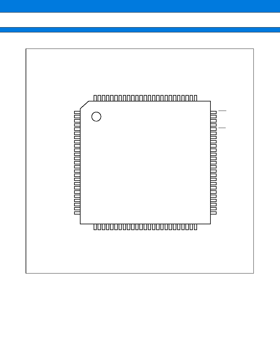
MB91260B Series
4
(Continued)
P25/SCK1
P26/INT6
P27/INT7
P50
P51/TIN0
P52/TIN1
P53/TIN2
P54/INT0
P55/INT1
P56/INT2
P57/INT3
PG0/CKI/INT4
PG1/PPG0/INT5
PG2
V
CC
V
SS
C
PG3/SIN2
PG4/SOT2
PG5/SCK2
P40
P41
P42
P43
P44
1
2
3
4
5
6
7
8
9
10
11
12
13
14
15
16
17
18
19
20
21
22
23
24
25
75
74
73
72
71
70
69
68
67
66
65
64
63
62
61
60
59
58
57
56
55
54
53
52
51
INIT
MD0
MD1
MD2
NMI
P77/ADTG2
P76/ADTG1
P75/ADTG0
P74/PWI1
V
SS
V
CC
P73/PWI0
P72/DTTI
P71/TOT2
P70/TOT1
P63/INT9
P62/INT8
P61/IC3
P60/IC2
P37/IC1
P36/IC0
P35/RTO5
P34/RTO4
P33/RTO3
P32/RTO2
100
99
98
97
96
95
94
93
92
91
90
89
88
87
86
85
84
83
82
81
80
79
78
77
76
P24/SO
T1
P23/SIN1
P22/SCK0
P21/SO
T0
P20/SIN0
P17
P16/PPG15
X0
X1
V
SS
V
CC
P15/PPG14
P14/PPG13
P13/PPG12
P12/PPG11
P11/PPG10
P10/PPG9
P07/PPG8
P06/PPG7
P05/PPG6
P04/PPG5
P03/PPG4
P02/PPG3
P01/PPG2
P00/PPG1
P45
P46
P47
PE1/AN11
PE0/AN10
A
VRH2
AC
C
AV
CC
A
VRH1
AV
SS
PD1/AN9
PD0/AN8
A
VRH0
PC7/AN7
PC6/AN6
PC5/AN5
PC4/AN4
PC3/AN3
PC2/AN2
PC1/AN1
PC0/AN0
V
CC
V
SS
P30/R
T
O
0
P31/R
T
O
1
26
27
28
29
30
31
32
33
34
35
36
37
38
39
40
41
42
43
44
45
46
47
48
49
50
(TOP VIEW)
(FPT-100-M05)
MB91260B Series
5
s
s
s
s
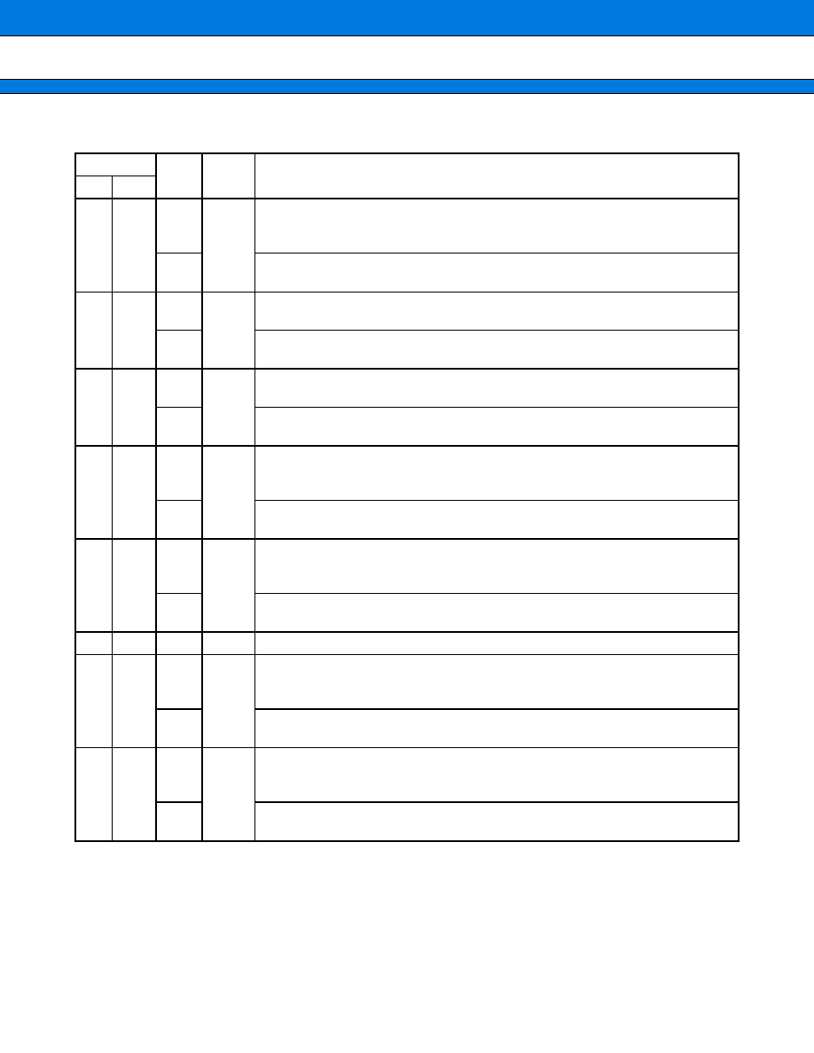
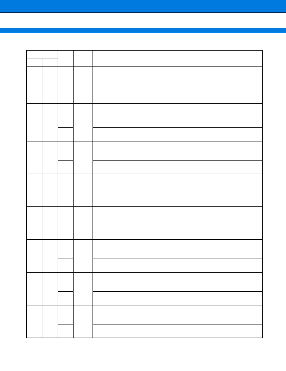
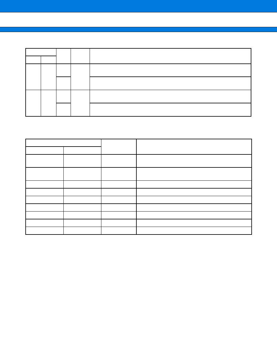
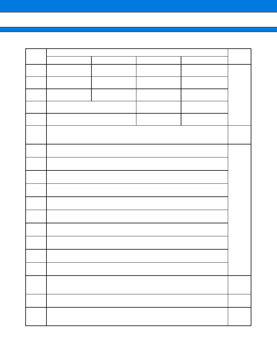
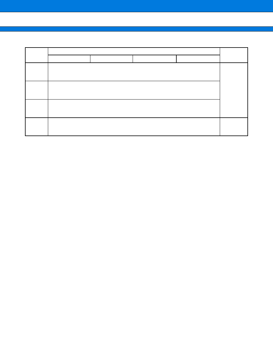
PIN DESCRIPTION
(Continued)
Pin no.
Pin
name
Circuit
type
Description
QFP LQFP
1
99
SIN1
D
UART1 data input terminal.
When use the terminal as data input of UART1, set the corresponding data
direction resister (DDR) to input.
P23
General purpose input/output port.
This function is always valid.
2
100
SOT1
D
UART1 data output terminal.
This function becomes valid when data output of UART1 is set to enabled.
P24
General purpose input/output port.
This function becomes valid when data output of UART1 is set to disabled.
3
1
SCK1
D
UART1 clock input/output terminal.
This function becomes valid when clock input/output is set to enabled.
P25
General purpose input/output port.
This function becomes valid when clock input/output is set to disabled.
4
2
INT6
E
External interrupt input terminal.
When use the terminal as external interrupt input, set the corresponding data
direction resister (DDR) to input.
P26
General purpose input/output port.
This function is always valid.
5
3
INT7
E
External interrupt input terminal.
When use the terminal as external interrupt input, set the corresponding data
direction resister (DDR) to input.
P27
General purpose input/output port.
This function is always valid.
6
4
P50
C
General purpose input/output port.
7
5
TIN0
C
External trigger input terminal of reload timer 0.
When use the terminal as trigger input, set the corresponding data
direction resister (DDR) to input.
P51
General purpose input/output port.
This function is always valid.
8
6
TIN1
C
External trigger input terminal of reload timer 1.
When use the terminal as external trigger input, set the corresponding data
direction resister (DDR) to input.
P52
General purpose input/output port.
This function is always valid.
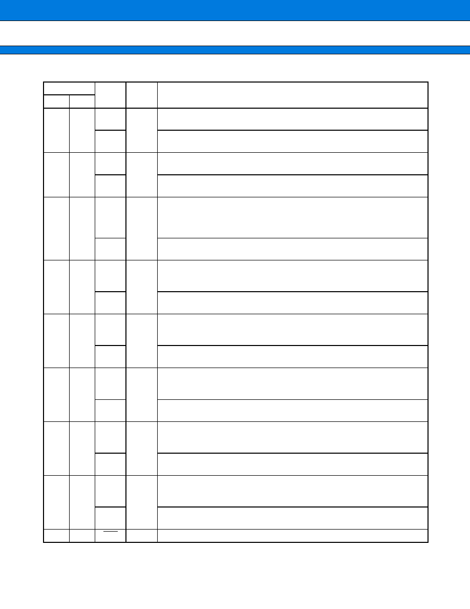
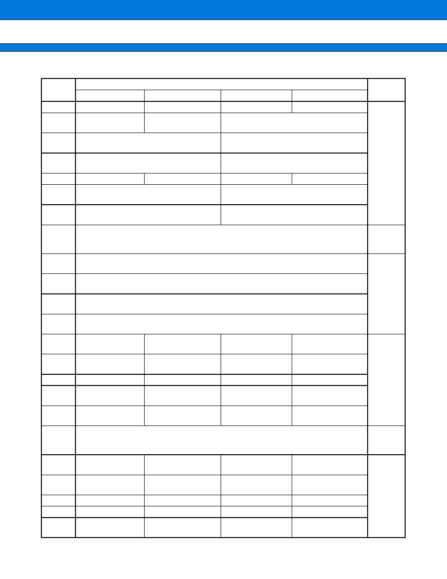
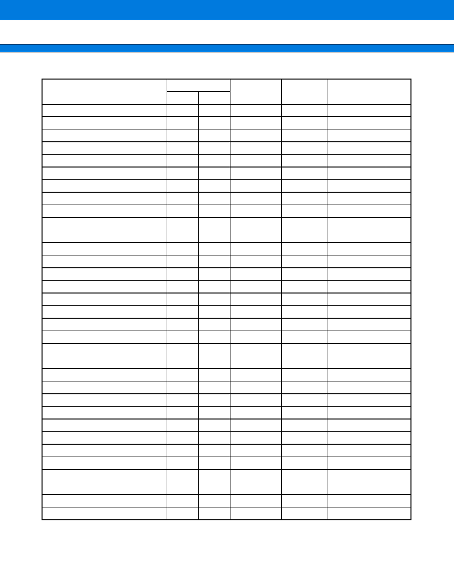
MB91260B Series
6
(Continued)
Pin no.
Pin
name
Circuit
type
Description
QFP
LQFP
9
7
TIN2
C
External trigger input terminal of reload timer 2.
When use the terminal as external trigger input, set the corresponding data
direction resister (DDR) to input.
P53
General purpose input/output port.
This function is always valid.
10
8
INT0
E
External interrupt input terminal.
When use the terminal as external interrupt input, set the corresponding data
direction resister (DDR) to input.
P54
General purpose input/output port.
This function is always valid.
11
9
INT1
E
External interrupt input terminal.
When use the terminal as external interrupt input, set the corresponding data
direction resister (DDR) to input.
P55
General purpose input/output port.
This function is always valid.
12
10
INT2
E
External interrupt input terminal.
When use the terminal as external interrupt input, set the corresponding data
direction resister (DDR) to input.
P56
General purpose input/output port.
This function is always valid.
13
11
INT3
E
External interrupt input terminal.
When use the terminal as external interrupt input, set the corresponding data
direction resister (DDR) to input.
P57
General purpose input/output port.
This function is always valid.
14
12
CKI
E
External clock input terminal for free-run timer.
When use the terminal as external clock input of free-run timer, set the
corresponding data direction resister (DDR) to input.
INT4
External interrupt input terminal.
When use the terminal as external interrupt input, set the corresponding data
direction resister (DDR) to input.
PG0
General purpose input/output port.
This function is always valid.
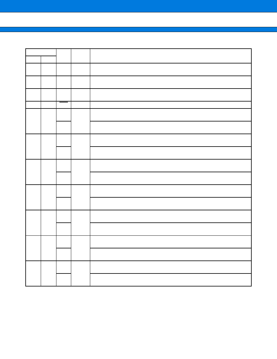
MB91260B Series
7
(Continued)
Pin no.
Pin
name
Circuit
type
Description
QFP
LQFP
15
13
PPG0
E
Output terminal of PPG timer 0.
This function becomes valid when output of PPG timer 0 is set to enabled.
INT5
External interrupt input terminal.
When use the terminal as external input, output of PPG timer 0 is set to disabled,
and set the corresponding data direction resister (DDR) to input.
PG1
General purpose input/output port.
This function becomes valid when output of PPG temer 0 is set to disabled.
16
14
PG2
C
General purpose input/output port.
20
18
SIN2
D
UART2 data input terminal.
When use the terminal as data input of UART2, set the corresponding data
direction resister (DDR) to input.
PG3
General purpose input/output port.
This function is always valid.
21
19
SOT2
D
UART2 data output terminal.
This function becomes valid when data output of UART2 is set to enabled.
PG4
General purpose input/output port.
This function becomes valid when data output of UART2 is set to disabled.
22
20
SCK2
D
UART2 clock input/output terminal.
This function becomes valid when clock input/output of UART2 is set to enabled.
PG5
General purpose input/output port.
This function becomes valid when clock input/output of UART2 is set to disabled.
23
21
P40
C
General purpose input/output port.
24
22
P41
C
General purpose input/output port.
25
23
P42
C
General purpose input/output port.
26
24
P43
C
General purpose input/output port.
27
25
P44
C
General purpose input/output port.
28
26
P45
C
General purpose input/output port.
29
27
P46
C
General purpose input/output port.
30
28
P47
C
General purpose input/output port.
31
29
AN11
G
Analog input terminal of A/D converter.
This function becomes valid when set the corresponding AICR2 resister to
analog input.
PE1
General purpose input/output port.
This function becomes valid when set the corresponding AICR2 resister to port.
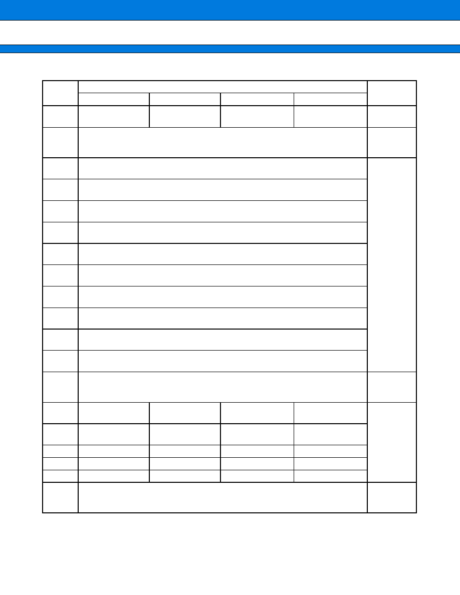
MB91260B Series
8
(Continued)
Pin no.
Pin
name
Circuit
type
Description
QFP
LQFP
32
30
AN10
G
Analog input terminal of A/D converter.
This function becomes valid when set the corresponding AICR2 resister to
analog input.
PE0
General purpose input/output port.
This function becomes valid when set the corresponding AICR2 resister to port.
38
36
AN9
G
Analog input terminal of A/D converter.
This function becomes valid when set the corresponding AICR1 resister to
analog input.
PD1
General purpose input/output port.
This function becomes valid when set the corresponding AICR1 resister to port.
39
37
AN8
G
Analog input terminal of A/D converter.
This function becomes valid when set the corresponding AICR1 resister to
analog input.
PD0
General purpose input/output port.
This function becomes valid when set the corresponding AICR1 resister to port.
41
39
AN7
G
Analog input terminal of A/D converter.
This function becomes valid when set the corresponding AICR0 resister to
analog input.
PC7
General purpose input/output port.
This function becomes valid when set the corresponding AICR0 resister to port.
42
40
AN6
G
Analog input terminal of A/D converter.
This function becomes valid when set the corresponding AICR0 resister to
analog input.
PC6
General purpose input/output port.
This function becomes valid when set the corresponding AICR0 resister to port.
43
41
AN5
G
Analog input terminal of A/D converter.
This function becomes valid when set the corresponding AICR0 resister to
analog input.
PC5
General purpose input/output port.
This function becomes valid when set the corresponding AICR0 resister to port.
44
42
AN4
G
Analog input terminal of A/D converter.
This function becomes valid when set the corresponding AICR0 resister to
analog input.
PC4
General purpose input/output port.
This function becomes valid when set the corresponding AICR0 resister to port.
45
43
AN3
G
Analog input terminal of A/D converter.
This function becomes valid when set the corresponding AICR0 resister to
analog input.
PC3
General purpose input/output port.
This function becomes valid when set the corresponding AICR0 resister to port.
MB91260B Series
9
(Continued)
Pin no.
Pin
name
Circuit
type
Description
QFP
LQFP
46
44
AN2
G
Analog input terminal of A/D converter.
This function becomes valid when set the corresponding AICR0 resister to
analog input.
PC2
General purpose input/output port.
This function becomes valid when set the corresponding AICR0 resister to port.
47
45
AN1
G
Analog input terminal of A/D converter.
This function becomes valid when set the corresponding AICR0 resister to
analog input.
PC1
General purpose input/output port.
This function becomes valid when set the corresponding AICR0 resister to port.
48
46
AN0
G
Analog input terminal of A/D converter.
This function becomes valid when set the corresponding AICR0 resister to
analog input.
PC0
General purpose input/output port.
This function becomes valid when set the corresponding AICR0 resister to port.
51
49
RTO0
J
Waveform generator output terminal of multi-function timer.
This terminal outputs waveform set at the waveform generator.
This function becomes valid when waveform generator output of multi-function
timer is set to enabled.
P30
General purpose input/output port.
This function becomes valid when output of waveform generator is set to disabled.
52
50
RTO1
J
Waveform generator output terminal of multi-function timer.
This terminal outputs waveform set at the waveform generator.
This function becomes valid when waveform generator output of multi-function
timer is set to enabled.
P31
General purpose input/output port.
This function becomes valid when output of waveform generator is set to disabled.
53
51
RTO2
J
Waveform generator output terminal of multi-function timer.
This terminal outputs waveform set at the waveform generator.
This function becomes valid when waveform generator output of multi-function
timer is set to enabled.
P32
General purpose input/output port.
This function becomes valid when output of waveform generator is set to disabled.
54
52
RTO3
J
Waveform generator output terminal of multi-function timer.
This terminal outputs waveform set at the waveform generator.
This function becomes valid when waveform generator output of multi-function
timer is set to enabled.
P33
General purpose input/output port.
This function becomes valid when output of waveform generator is set to disabled.
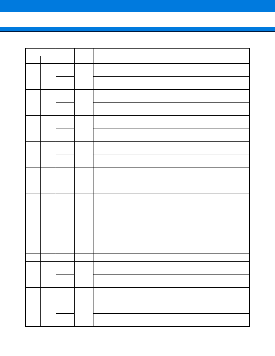
MB91260B Series
10
(Continued)
Pin no.
Pin
name
Circuit
type
Description
QFP
LQFP
55
53
RTO4
J
Waveform generator output terminal of multi-function timer.
This terminal outputs waveform set at the waveform generator.
This function becomes valid when waveform generator output of multi-function
timer is set to enabled.
P34
General purpose input/output port.
This function becomes valid when output of waveform generator is set to disabled.
56
54
RTO5
J
Waveform generator output terminal of multi-function timer.
This terminal outputs waveform set at the waveform generator.
This function becomes valid when waveform generator output of multi-function
timer is set to enabled.
P35
General purpose input/output port.
This function becomes valid when output of waveform generator is set to disabled.
57
55
IC0
D
Trigger input terminal of input capture 0.
When use the terminal as trigger input of input capture, set the corresponding data
direction resister (DDR) to input.
P36
General purpose input/output port.
This function is always valid.
58
56
IC1
D
Trigger input terminal of input capture 1.
When use the terminal as trigger input of input capture, set the corresponding data
direction resister (DDR) to input.
P37
General purpose input/output port.
This function is always valid.
59
57
IC2
D
Trigger input terminal of input capture 2.
When use the terminal as trigger input of input capture, set the corresponding data
direction resister (DDR) to input.
P60
General purpose input/output port.
This function is always valid.
60
58
IC3
D
Trigger input terminal of input capture 3.
When use the terminal as trigger input of input capture, set the corresponding data
direction resister (DDR) to input.
P61
General purpose input/output port.
This function is always valid.
61
59
INT8
E
External interrupt input terminal.
When use the terminal as external input, set the corresponding data direction
resister (DDR) to input.
P62
General purpose input/output port.
This function is always valid.
62
60
INT9
E
External interrupt input terminal.
When use the terminal as external input, set the corresponding data direction
resister (DDR) to input.
P63
General purpose input/output port.
This function is always valid.
MB91260B Series
11
(Continued)
Pin no.
Pin
name
Circuit
type
Description
QFP
LQFP
63
61
TOT1
C
Output terminal of reload timer 1.
This function becomes valid when reload timer output is set to enabled.
P70
General purpose input/output port.
This function becomes valid when reload timer output is set to disabled.
64
62
TOT2
C
Output terminal of reload timer 2.
This function becomes valid when reload timer output is set to enabled.
P71
General purpose input/output port.
This function becomes valid when reload timer output is set to disabled.
65
63
DTTI
D
Outputcontrol input terminal of waveform generator output terminal RTO0 to
RTO5 of multi-function timer.
This function becomes valid when DTTI input is set to enabled by waveform
generator of multi-function timer.
P72
General purpose input/output port.
This function is always valid.
66
64
PWI0
D
Pulse width counter input terminal of PWC timer 0.
This function becomes valid when pulse width counter input of PWC timer 0 is
set to enabled.
P73
General purpose input/output port.
This function is always valid.
69
67
PWI1
D
Pulse width counter input terminal of PWC timer 1.
This function becomes valid when pulse width counter input of PWC timer 1 is
set to enabled.
P74
General purpose input/output port.
This function is always valid.
70
68
ADTG0
C
External trigger input terminal of A/D converter 0.
When use the external trigger as activation factor of A/D convertor, set the
corresponding data direction resister (DDR) to input.
P75
General purpose input/output port.
This function is always valid.
71
69
ADTG1
C
External trigger input terminal of A/D converter 1.
When use the external trigger as activation factor of A/D convertor, set the
corresponding data direction resister (DDR) to input.
P76
General purpose input/output port.
This function is always valid.
72
70
ADTG2
C
External trigger input terminal of A/D converter 2.
When use the external trigger as activation factor of A/D convertor, set the
corresponding data direction resister (DDR) to input.
P77
General purpose input/output port.
This function is always valid.
73
71
NMI
H
NMI (Non Maskable Interrupt) input terminal.
MB91260B Series
12
(Continued)
Pin no.
Pin
name
Circuit
type
Description
QFP
LQFP
74
72
MD2
K
Mode terminal 2.
Set operating mode. Connect to V
CC
or V
SS
.
75
73
MD1
K
Mode terminal 1.
Set operating mode. Connect to V
CC
or V
SS
.
76
74
MD0
K
Mode terminal 0.
Set operating mode. Connect to V
CC
or V
SS
.
77
75
INIT
I
External reset input terminal.
78
76
PPG1
C
Output terminal of PPG timer 1.
This function becomes valid when output of PPG timer 1 is set to enabled.
P00
General purpose input/output port.
This function becomes valid when output of PPG timer 1 is set to disabled.
79
77
PPG2
C
Output terminal of PPG timer 2.
This function becomes valid when output of PPG timer 2 is set to enabled.
P01
General purpose input/output port.
This function becomes valid when output of PPG timer 2 is set to disabled.
80
78
PPG3
C
Output terminal of PPG timer 3.
This function becomes valid when output of PPG timer 3 is set to enabled.
P02
General purpose input/output port.
This function becomes valid when output of PPG timer 3 is set to disabled.
81
79
PPG4
C
Output terminal of PPG timer 4.
This function becomes valid when output of PPG timer 4 is set to enabled.
P03
General purpose input/output port.
This function becomes valid when output of PPG timer 4 is set to disabled.
82
80
PPG5
C
Output terminal of PPG timer 5.
This function becomes valid when output of PPG timer 5 is set to enabled.
P04
General purpose input/output port.
This function becomes valid when output of PPG timer 5 is set to disabled.
83
81
PPG6
C
Output terminal of PPG timer 6.
This function becomes valid when output of PPG timer 6 is set to enabled.
P05
General purpose input/output port.
This function becomes valid when output of PPG timer 6 is set to disabled.
84
82
PPG7
C
Output terminal of PPG timer 7.
This function becomes valid when output of PPG timer 7 is set to enabled.
P06
General purpose input/output port.
This function becomes valid when output of PPG timer 7 is set to disabled.
MB91260B Series
13
(Continued)
Pin no.
Pin
name
Circuit
type
Description
QFP
LQFP
85
83
PPG8
C
Output terminal of PPG timer 8.
This function becomes valid when output of PPG timer 8 is set to enabled.
P07
General purpose input/output port.
This function becomes valid when output of PPG timer 8 is set to disabled.
86
84
PPG9
C
Output terminal of PPG timer 9.
This function becomes valid when output of PPG timer 9 is set to enabled.
P10
General purpose input/output port.
This function becomes valid when output of PPG timer 9 is set to disabled.
87
85
PPG10
C
Output terminal of PPG timer 10.
This function becomes valid when output of PPG timer 10 is set to enabled.
P11
General purpose input/output port.
This function becomes valid when output of PPG timer 10 is set to disabled.
88
86
PPG11
C
Output terminal of PPG timer 11.
This function becomes valid when output of PPG timer 11 is set to enabled.
P12
General purpose input/output port.
This function becomes valid when output of PPG timer 11 is set to disabled.
89
87
PPG12
C
Output terminal of PPG timer 12.
This function becomes valid when output of PPG timer 12 is set to enabled.
P13
General purpose input/output port.
This function becomes valid when output of PPG timer 12 is set to disabled.
90
88
PPG13
C
Output terminal of PPG timer 13.
This function becomes valid when output of PPG timer 13 is set to enabled.
P14
General purpose input/output port.
This function becomes valid when output of PPG timer 13 is set to disabled.
91
89
PPG14
C
Output terminal of PPG timer 14.
This function becomes valid when output of PPG timer 14 is set to enabled.
P15
General purpose input/output port.
This function becomes valid when output of PPG timer 14 is set to disabled.
94
92
X1
A
Main clock oscillation output terminal.
95
93
X0
A
Main clock oscillation input terminal.
96
94
PPG15
C
Output terminal of PPG timer 15.
This function becomes valid when output of PPG timer 15 is set to enabled.
P16
General purpose input/output port.
This function becomes valid when output of PPG timer 15 is set to disabled.
97
95
P17
C
General purpose input/output port.
98
96
SIN0
D
UART0 data input terminal.
When use the terminal as data input of UART0, set the corresponding data
direction resister (DDR) to input.
P20
General purpose input/output port.
This function is always valid.
MB91260B Series
14
(Continued)
∑
∑
∑
∑
Power supply and GND pins
Pin no.
Pin
name
Circuit
type
Description
QFP
LQFP
99
97
SOT0
D
UART0 data output terminal.
This function becomes valid when data output of UART0 is set to enabled.
P21
General purpose input/output port.
This function becomes valid when data output of UART0 is set to disabled.
100
98
SCK0
D
UART0 clock input/output terminal.
This function becomes valid when clock input/output of UART0 is set to enabled.
P22
General purpose input/output port.
This function becomes valid when clock input/output of UART0 is set to disabled.
Pin no.
Pin name
Description
QFP
LQFP
18, 50, 68, 93
16, 48, 66, 91
Vss
GND pins.
Apply equal potential to all of the pins.
17, 49, 67, 92
15, 47, 65, 90
Vcc
Power supply pin.
Apply equal potential to all of the pins.
35
33
AVcc
Analog power supply pin for A/D converter.
33
31
AVRH2
Analog reference power supply pin for A/D converter 2.
36
34
AVRH1
Analog reference power supply pin for A/D converter 1.
40
38
AVRH0
Analog reference power supply pin for A/D converter 0.
37
35
AVss
Analog GND pin for A/D converter.
19
17
C
Condencer connection pin for internal regulator.
34
32
ACC
Condencer connection pin for analog.
MB91260B Series
15
s
s
s
s
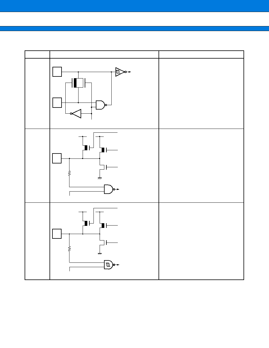
I/O CIRCUIT TYPE
(Continued)
Type
Circuit type
Remarks
A
∑ Oscillation circuit
∑ Oscillation feedback resistance :
approx. 1 M
C
∑ CMOS level output
∑ CMOS level input.
∑ With standby control
∑ With Pull-up control
∑ Pull-up resistance value
=
approx. 50 k
(Typ)
∑ I
OL
=
4 mA
D
∑ CMOS level output
∑ CMOS level hysteresis input.
∑ With standby control
∑ With Pull-up control
∑ Pull-up resistance value
=
approx. 50 k
(Typ)
∑ I
OL
=
4 mA
X1
X0
Clock input
Standby control
R
P-ch
N-ch
P-ch
Digital input
Pull-up control
Digital output
Digital output
Standby control
R
P-ch
P-ch
N-ch
Digital input
Pull-up control
Digital output
Digital output
Standby control
MB91260B Series
16
(Continued)
Type
Circuit type
Remarks
E
∑ CMOS level output
∑ CMOS level hysteresis input.
∑ Without standby control
∑ With Pull-up control
∑ Pull-up resistance value
=
approx. 50 k
(Typ)
∑ I
OL
=
4 mA
G
∑ Analog/CMOS level input/output pin
∑ CMOS level output
∑ CMOS level input.
(attached with standby control)
∑ Analog input
(Analog input is enabled when AICR's
corresponding bit is set to "1".)
∑ I
OL
=
4 mA
H
∑ CMOS level hysteresis input.
∑ Without standby control
R
P-ch
N-ch
P-ch
Digital input
Digital output
Digital output
Pull-up control
R
P-ch
N-ch
Analog input
Digital input
Digital output
Digital output
Standby control
R
N-ch
P-ch
Digital input
MB91260B Series
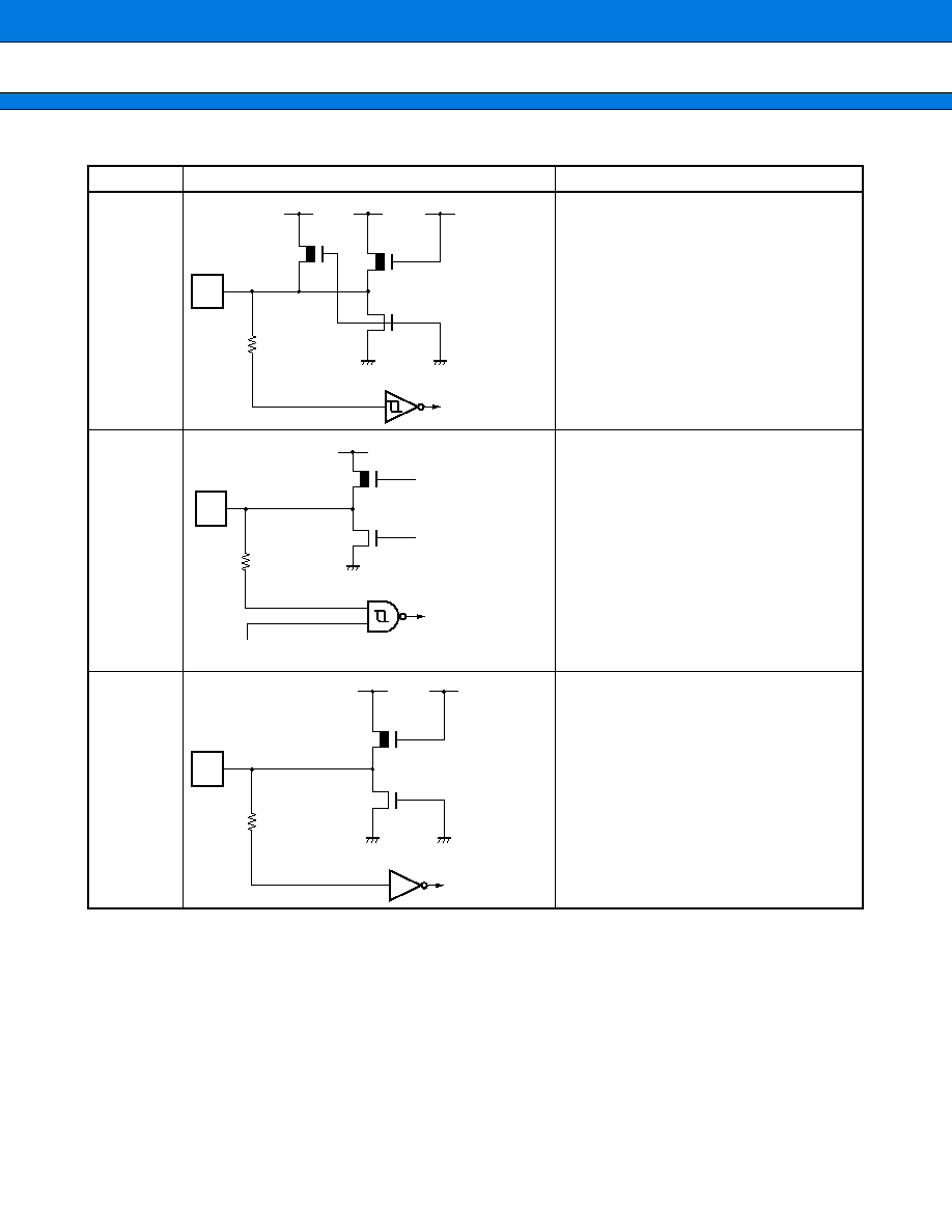
17
(Continued)
Type
Circuit type
Remarks
I
∑ CMOS level hysteresis input.
∑ With pull-up resistor
∑ Pull-up resistance value
=
approx. 50 k
(Typ)
∑ Without standby control
J
∑ CMOS level output
∑ CMOS level hysteresis input.
∑ With standby control
∑ I
OL
=
12 mA
K
∑ CMOS level input.
∑ Without standby control
R
P-ch
P-ch
N-ch
Digital input
R
P-ch
N-ch
Digital output
Digital output
Digital input
Standby control
R
P-ch
N-ch
Digital input

MB91260B Series
18
s
s
s
s
HANDLING DEVICES
∑
Preventing Latchup
Latch-up may occur in a CMOS IC if a voltage greater than V
CC
or less than V
SS
is applied to an input or output
pin or if an above-rating voltage is applied between V
CC
and V
SS
.
A latchup, if it occurs, significantly increases the power supply current and may cause thermal destruction of an
element. When you use a CMOS IC, be very careful not to exceed the maximum rating.
∑
Treatment of Unused Input Pins
Do not leave an unused input pin open, since it may cause a malfunction. Handle by, for example, using a pull-
up or pull-down resistor.
∑
About power supply pins
In products with multiple V
CC
or V
SS
pins, the pins of the same potential are internally connected in the device
to avoid abnormal operations including latch-up. However you must connect the pins to external a same potential
power supply and a ground line to lower the electro-magnetic emission level to prevent abnormal operation of
strobe signals caused by the rise in the ground level, and to conform to the total current rating.
The power pins should be connected to V
CC
and V
SS
of this device at the lowest possible impedance from the
current supply source.
It is also advisable to connect a ceramic bypass capacitor of approximately 0.1
µ
F between V
CC
and V
SS
near
this device.
∑
About Crystal oscillator circuit
Noise near the X0 and X1 pin may cause the device to malfunction.
Design the circuit board so that X0 and X1, the crystal oscillator (or ceramic oscillator), and the bypass capacitor
to ground are located as close to the device as possible.
It is strongly recommended to design the PC board artwork with the X0 and XI pins surrounded by ground plane
because stable operation can be expected with such a layout.
∑
Mode pins (MD0 to MD2)
These pins should be connected directly to V
CC
or V
SS
.
To prevent the device erroneously switching to test mode due to noise, design the printed circuit board such that
the distance between the mode pins and V
CC
or V
SS
is as short as possible and the connection impedance is low.
∑
Operation at start-up
Be sure to execute setting initialized reset (INIT) with INIT pin immediately after start-up.
Also, in order to provide a delay while the oscillator circuit stabilize immediately after start-up, maintain the "L"
level input to the INIT pin for the required stabilization wait time.
(For INIT via the INIT pin, the oscillation stabilization wait time setting is initialized to the minimum value.)
∑
About oscillation input at power on
When turning the power on, maintain clock input until the device is released from the oscillation stabilization
wait state.
MB91260B Series
19
∑
Caution operation during PLL clock mode
Even if the oscillator comes off or the clock input stops with the PLL clock selected for this device, the device
may continue to operate at the free-run frequency of the PLL's internal self-oscillating oscillator circuit.
Performance of this operation, however, cannot be guaranteed.
∑
External clock
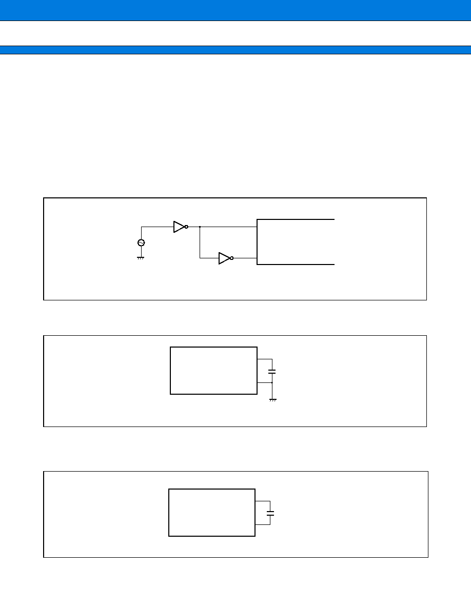
When external clock is selected, the opposite phase clock to X0 pin must be supplied to X1 pin simultaneously.
If the STOP mode (oscillation stop mode) is used simultaneously, the X1 pin is stopped with the "H" output. So,
when STOP mode is specified, approximately 1 k
of resistance should be added externally to avoid the conclift
of output.
The following figure shows using an external clock.
∑
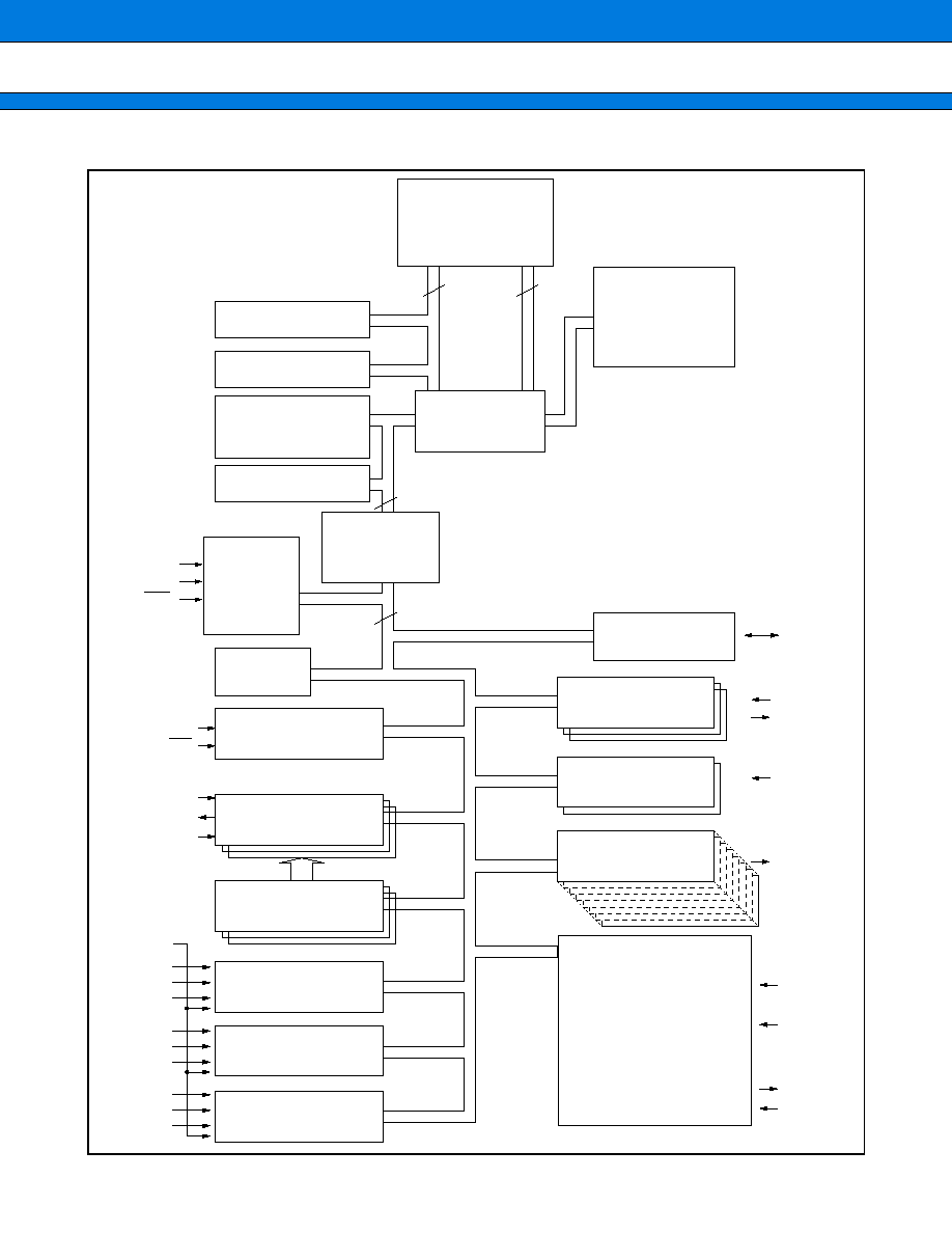
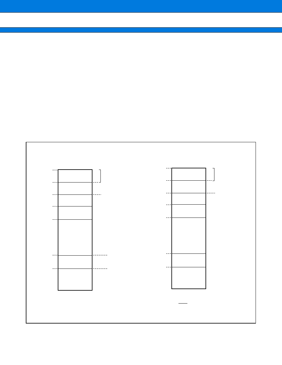
C pin
A bypass capacitor of approximately 0.1
µ
F should be connected the C pin for built-in regulator.
∑
ACC pin
A capacitor of approximately 0.1
µ
F should be inserted between the ACC pin and the AVcc pin as this product
has built-in A/D convertor.
X0
X1
Using an external clock
MB91260B series
C
0.1
µ
F
GND
V
SS
MB91260B series
ACC
0.1
µ
F
AV
SS
MB91260B series

MB91260B Series
20
∑
Clock control block
Take the oscillation stabilization wait time during Low level input to the INIT pin.
∑
Switch shared port function
To switch between the use as a port and the use as a dedicated pin, use the port function register (PFR).
∑
Low Power Consumption Mode
(1) To enter the standby mode, use the synchronous standby mode (set with the SYNCS bit as bit 8 in the TBCR:
or time-base counter control register) and be sure to use the following seaquence
In addition, please set I flag, ILM, and ICR to diverge to the interruption handler that is the return factor after
the standby returns.
(2) Please do not do the following when the monitor debugger is used.
∑
Break point setting for above instruction lines
∑
Step execution for above instruction lines
∑
Notes on the PS register
As the PS register is processed by some instructions in advance, exception handling below may cause the
interrupt handling routine to break when the debugger is used or the display contents of flags in the PS register
to be updated.
As the microcontroller is designed to carry out reprocessing correctly upon returning from such an EIT event, it
performs operations before and after the EIT as specified in either case.
1. The following operations are performed when the instruction followed by a DIV0U/DIV0S instruction results
in : (a) acceptance of a user interrupt or NMI, (b) step execution, or (c) a break at a data event or emulator menu.
(1) The D0 and D1 flags are updated in advance.
(2) An EIT handling routine (user interrupt, NMI, or emulator) is executed.
(3) Upon returning from the EIT, the DIV0U/DIV0S instruction is executed and the D0 and D1 flags are
updated to the same values as in (1).
2. The following operations are performed when the ORCCR/STILM/MOVRi and PS instructions are executed
to enable interruptions when a user interrupt or NMI trigger even has occurred.
(1) The PS register is updated in advance.
(2) An EIT handling routine (user interrupt, NMI) is executed.
(3) Upon returning from the EIT, the above instructions are executed and the PS register is updated to the
same value as in (1).
(LDI
#value_of_standby, R0)
: Value_of standby is write data to STCR.
(LDI
#_STCR, R12)
: _STCR is address (481H) of STCR.
STB
R0, @R12
: Writing to standby control register (STCR)
LDUB @R12, R0
: STCR read for synchronous standby
LDUB @R12, R0
: Dummy re-read of STCR
NOP
: NOP
◊
5 for arrangement of timing
NOP
NOP
NOP
NOP

MB91260B Series
21
∑
Watch dog timer
The watchdog timer built in this model monitors a program that it defers a reset within a certain period of time.
The watchdog timer resets the CPU if the program runs out of controls, preventing the reset defer function from
being executed. Once the function of the watchdog timer is enabled, therefore, the watchdog timer keeps on
operating programs until it resets the CPU.
As an exception, the watchdog timer defers a reset timing automatically under the condition in which the CPU
stops program execution.

MB91260B Series
22
s
s
s
s
NOTE ON DEBUGGER
∑
Step execution of RETI command
If an interrupt occurs frequently during step execution, the corresponding interrupt handling routine is executed
repeatedly after step execution.
This will prevent the main routine and low-interrupt-level programs from being executed.
Do not execute step of RETI instruction for escape.
Disable the corresponding interrupt and execute debugger when the corresponding interrupt handling routine
no longer needs debugging.
∑
Operand break
Do not apply a data event break to access to the area containing the address of a system stack pointer.
∑
Execution in an unused area of FLASH memory
Accidentally executing an instruction in an unused area of FLASH memory (with data placed at 0XFFFF) prevents
breaks from being accepted.
To prevent this, the code event address mask function of the debugger should be used to cause a break when
accessing an instruction in an unused area.
∑
Power-on debugging
All of the following three conditions must be satisfied when the power supply is turned off by power-on debugging.
(1) The time for the user power to fall from 0.9 VCC to 0.5 VCC is 25
µ
s or longer.
Note : In a dual-power system, VCC indicates the external I/O power supply voltage.
(2) CPU operating frequency must be higher than 1 MHz.
(3) During execution of user program
∑
Interrupt handler for NMI request (tool)
Add the following program to the interrupt handler to prevent the device from malfunctioning in case the factor
flag to be set only in response to a break request from the ICE is set, for example, by an adverse effect of noise
to the DSU pin while the ICE is not connected. Enable to use the ICE while adding this program.
Additional location
Next interrupt handler
Additional program
Interrupt source
: NMI request (tool)
Interrupt number
: #13 (decimal) , 0D
H
(hexa decimal)
Offset
: 3C8
H
Address TBR is default
: 000FFFC8
H
STM
(R0, R1)
LDI
#B00
H
, R0;
: B00
H
is the address of DSU break factor register.
LDI
#0, R1
STB
R1, @R0
: Clear the break factor register.
LDM
(R0, R1)
RETI
MB91260B Series
23
s
s
s
s
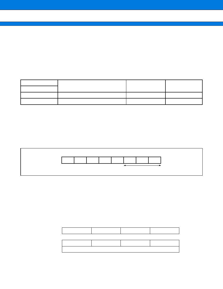
BLOCK DIAGRAM
ROM 128 KB/
FLASH 256 KB
RAM 8 KB
DMAC 5 ch
3 ch
UART
X0, X1
MD0 ~ MD2
INIT
INT0 ~ INT9
NMI
SIN0 ~ SIN2
SOT0 ~ SOT2
SCK0 ~ SCK2
AV
CC
ADTG0
AN0 ~ AN7
AVRH0
ADTG1
AVRH1
AN8, AN9
ADTG2
AVRH2
AN10, AN11
PORT
TIN0 ~ TIN2
TOT1, TOT2
PWI0, PWI1
PPG0 ~ PPG15
CKI
IC0 ~ IC3
RTO0 ~ RTO5
DTTI
32
32
16
32
Bit search
SUM of products macro
Clock
control
Interrupt
controller
10 ch
External interrupt
3 ch
U timer
FR60 Lite CPU core
Bus converter
Port I/F
3 ch
reload timer
8 ch
8/16 PPG timer
Free-run timer 1 ch
Input capture 4 ch
Output compare 6 ch
Waveform generator
Multi-function timer
8 ch input
8/10 bit A/D-0
2 ch input
8/10 bit A/D-1
2 ch input
8/10 bit A/D-2
32
16
Adapter
2 ch
PWC timer
MB91260B Series
24
s
s
s
s
MEMORY SPACE
1.
Memory space
The FR family has 4 Gbytes of logical address space (2
32
addresses) available to the CPU by linear access.
∑ Direct Addressing Areas
The following address space areas are used as I/O areas.
These areas are called direct addressing areas, in which the address of an operand can be specified directly
during an instruction.
The size of directly addressable areas depends on the data size to be being accessed as follows.
byte data access
: 000-0FF
H
half word data access
: 000-1FF
H
word data access
: 000-3FF
H
2.
Memory Map
000E 0000
H
0000 0000
H
0000 0400
H
0001 0000
H
0003 E000
H
0004 0000
H
0010 0000
H
FFFF FFFF
H
I/O
I/O
Single chip mode
Refer to I/O Map
Direct
addressing area
Access
disallowed
Internal RAM
8 KB
Access
disallowed
Internal RAM
128 KB
Access
disallowed
Each mode is set depending on the mode vector fetched after the INIT signal is nagated.
(Refer to
MODE SETTINGS for mode setting.)
MB91263B
000C 0000
H
0000 0000
H
0000 0400
H
0001 0000
H
0003 E000
H
0004 0000
H
0010 0000
H
FFFF FFFF
H
I/O
I/O
Single chip mode
Refer to I/O Map
Direct
addressing area
Access
disallowed
Internal RAM
8 KB
Access
disallowed
Internal RAM
256 KB
Access
disallowed
MB91F264B
MB91260B Series
25
s
s
s
s
MODE SETTINGS
The FR family uses mode pins (MD2 to MD0) and a mode data to set the operation mode.
1.
Mode Pins
The MD2, MD1, and MD0 pins specify how the mode vector fetch and reset vector fetch is performed.
Setting is prohibited other than that shown in the following table.
2.
Mode data
Data written to the internal mode register (MODR) by a mode vector fetch is called mode data.
After an operation mode has been set in the mode register, the device operates in the operation mode.
The mode data is set by all reset source. User programs cannot set data to the mode register.
<Details of mode data description>
[bit31-24] Reserved bit
Be sure to set this bit to "00000111".
Operation is not guaranteed when any value other than "00000111" is set.
3.
Note
Mode data set in the mode vector must be placed as byte data at 0X000FFFF8.
Use the highest byte from bit 31 to bit 24 for placement as the FR family uses the big endian method for byte
endian.
Mode Pins
Mode name
Reset vector access
area
Remarks
MD2
MD1
MD0
0
0
0
Internal ROM mode vector
Internal
1
0
0
Flash serial write mode
31 24 23
16 15
8 7
0
Incorrect 0x000FFFF8
XXXXXXXX
XXXXXXXX
XXXXXXXX
Mode Data
Correct
0x000FFFF8
Mode Data
XXXXXXXX
XXXXXXXX
XXXXXXXX
0x000FFFFC
Reset Vector
31
30
29
28
27
26
25
24
0
0
0
0
0
1
1
1
Operation mode setting bits
MB91260B Series
26
s
s
s
s
I/O MAP
This shows the location of the various peripheral resource registers in the memory space.
Note : Initial values of register bits are represented as follows :
" 1 "
: Initial Value : " 1 "
" 0 "
: Initial Value : " 0 "
" X "
: Initial Value : " undefined "
" - "
: No physical register at this location
Address
Register
Block
+
+
+
+
0
+
+
+
+
1
+
+
+
+
2
+
+
+
+
3
000000
H
PDR0 [R/W]B
XXXXXXXX
PDR1 [R/W]B
XXXXXXXX
PDR2 [R/W]B
XXXXXXXX
PDR3 [R/W]B
XXXXXXXX
Port data register
Read/write attribute, Access unit
(B : byte, H : half word, W : word)
Initial value after a reset
Register name (First-column register at address 4n; second-column
register at address 4n
+
2)
Location of left-most register (When using word access, the register in
column 1 is in the MSB side of the data.)
MB91260B Series
27
(Continued)
Address
Register
Block
+
+
+
+
0
+
+
+
+
1
+
+
+
+
2
+
+
+
+
3
000000
H
PDR0 [R/W] B
XXXXXXXX
PDR1 [R/W] B
XXXXXXXX
PDR2 [R/W] B
XXXXXXXX
PDR3 [R/W] B
XXXXXXXX
Port data register
000004
H
PDR4 [R/W] B
XXXXXXXX
PDR5 [R/W] B
XXXXXXXX
PDR6 [R/W] B
----XXXX
PDR7 [R/W] B
XXXXXXXX
000008
H
00000C
H
PDRC [R/W] B
XXXXXXXX
PDRD [R/W] B
------XX
PDRE [R/W] B
------XX
000010
H
PDRG [R/W] B
--XXXXXX
000014
H
to
00003C
H
Reserved
000040
H
EIRR0 [R/W] B, H, W
00000000
ENIR0 [R/W] B, H, W
00000000
ELVR0 [R/W] B, H, W
00000000 00000000
External interrupt
(INT0 to INT7)
000044
H
DICR [R/W] B, H, W
-------0
HRCL [R/W, R]
B, H, W
0--11111
Delay interrupt/
Hold request
000048
H
TMRLR0 [W] H, W
XXXXXXXX XXXXXXXX
TMR0 [R] H, W
XXXXXXXX XXXXXXXX
Reload
timer 0
00004C
H
TMCSR0 [R/W, R] B, H, W
---00000 00000000
000050
H
TMRLR1 [W] H, W
XXXXXXXX XXXXXXXX
TMR1 [R] H, W
XXXXXXXX XXXXXXXX
Reload
timer 1
000054
H
TMCSR1 [R/W, R] B, H, W
---00000 00000000
000058
H
TMRLR2 [W] H, W
XXXXXXXX XXXXXXXX
TMR2 [R] H, W
XXXXXXXX XXXXXXXX
Reload
timer 2
00005C
H
TMCSR2 [R/W, R] B, H, W
---00000 00000000
000060
H
SSR0 [R/W, R] B, H, W
00001000
SIDR0 [R]/SODR0[W]
B, H, W
XXXXXXXX
SCR0 [R/W] B, H, W
00000100
SMR0 [R/W, W] B, H, W
00--0-0-
UART0
000064
H
UTIM0 [R] H / UTIMR0 [W] H
00000000 00000000
DRCL0 [W] B
--------
UTIMC0 [R/W] B
0--00001
U-timer 0
000068
H
SSR1 [R/W, R] B, H, W
00001000
SIDR1 [R]/SODR1[W]
B, H, W
XXXXXXXX
SCR1 [R/W] B, H, W
00000100
SMR1 [R/W] B, H, W
00--0-0-
UART1
00006C
H
UTIM1 [R] H / UTIMR1 [W] H
00000000 00000000
DRCL1 [W] B
--------
UTIMC1 [R/W] B
0--00001
U-timer 1
000070
H
SSR2 [R/W, R] B, H, W
00001000
SIDR2 [R]/SODR2[W]
B, H, W
XXXXXXXX
SCR2 [R/W] B, H, W
00000100
SMR2 [R/W] B, H, W
00--0-0-
UART2
000074
H
UTIM2 [R] H / UTIMR2 [W] H
00000000 00000000
DRCL2 [W] B
--------
UTIMC2 [R/W] B
0--00001
U-timer 2
MB91260B Series
28
(Continued)
Address
Register
Block
+
+
+
+
0
+
+
+
+
1
+
+
+
+
2
+
+
+
+
3
000078
H
ADCH0 [R/W] B, H, W
XX000000
ADMD0 [R/W] B, H, W
00001111
ADCD01 [R] B, H, W
XXXXXXXX
ADCD00 [R] B, H, W
XXXXXXXX
A/D
converter 0/
AICR0
00007C
H
ADCS0 [R/W, W] B, H, W
00000X00
AICR0 [R/W] B, H, W
00000000
000080
H
ADCH1 [R/W] B, H, W
XXXX0XX0
ADMD1 [R/W] B, H, W
00001111
ADCD11 [R] B, H, W
XXXXXXXX
ADCD10 [R] B, H, W
XXXXXXXX
A/D
converter 1/
AICR1
000084
H
ADCS1 [R/W, W] B, H, W
00000X00
AICR1 [R/W] B, H, W
------00
000088
H
ADCH2 [R/W] B, H, W
XXXX0XX0
ADMD2 [R/W] B, H, W
00001111
ADCD21 [R] B, H, W
XXXXXXXX
ADCD20 [R] B, H, W
XXXXXXXX
A/D
converter 2/
AICR2
00008C
H
ADCS2 [R/W, W] B, H, W
00000X00
AICR2 [R/W] B, H, W
------00
000090
H
OCCPBH0, OCCPBL0[W]/
OCCPH0, OCCPL0[R] H, W
00000000 00000000
OCCPBH1, OCCPBL1[W]/
OCCPH1, OCCPL1 [R] H, W
00000000 00000000
OCU
000094
H
OCCPBH2, OCCPBL2[W]/
OCCPH2, OCCPL2 [R] H, W
00000000 00000000
OCCPBH3, OCCPBL3[W]/
OCCPH3, OCCPL3 [R] H, W
00000000 00000000
000098
H
OCCPBH4, OCCPBL4[W]/
OCCPH4, OCCPL4 [R] H, W
00000000 00000000
OCCPBH5, OCCPBL5[W]/
OCCPH5, OCCPL5 [R] H, W
00000000 00000000
00009C
H
OCSH1 [R/W] B, H, W
X1100000
OCSL0 [R/W] B, H, W
00001100
OCSH3 [R/W]
B, H, W
X1100000
OCSL2 [R/W]
B, H, W
00001100
0000A0
H
OCSH5 [R/W] B, H, W
X1100000
OCSL4 [R/W] B, H, W
00001100
OCMOD [R/W]
B, H, W
XX000000
0000A4
H
CPCLRBH, CPCLRBL[W]/
CPCLRH, CPCLRL[R] H, W
11111111 11111111
TCDTH, TCDTL [R/W] H, W
00000000 00000000
free-run
timer
0000A8
H
TCCSH [R/W] B, H, W
00000000
TCCSL [R/W] B, H, W
01000000
ADTRGC [R/W]
B, H, W
XXXX0000
0000AC
H
IPCPH0, IPCPL0 [R] H, W
XXXXXXXX XXXXXXXX
IPCPH1, IPCPL1 [R] H, W
XXXXXXXX XXXXXXXX
ICU
0000B0
H
IPCPH2, IPCPL2 [R] H, W
XXXXXXXX XXXXXXXX
IPCPH3, IPCPL3 [R] H, W
XXXXXXXX XXXXXXXX
0000B4
H
PICSH01 [W] B, H, W
000000--
PICSL01 [R/W] B, H, W
00000000
ICSH23 [R] B, H, W
XXXXXX00
ICSL23 [R/W]
B, H, W
00000000
0000B8
H
EIRR1 [R/W] B, H, W
------00
ENIR1 [R/W] B, H, W
------00
ELVR1 [R/W] B, H, W
-------- ----0000
External interrupt
(INT8, INT9)
MB91260B Series
29
(Continued)
Address
Register
Block
+
+
+
+
0
+
+
+
+
1
+
+
+
+
2
+
+
+
+
3
0000BC
H
TMRRH0, TMRRL0 [R/W] H, W
XXXXXXXX XXXXXXXX
TMRRH1, TMRRL1 [R/W] H, W
XXXXXXXX XXXXXXXX
Waveform
generator
0000C0
H
TMRRH2, TMRRL2 [R/W] H, W
XXXXXXXX XXXXXXXX
0000C4
H
DTCR0 [R/W] B, H, W
00000000
DTCR1 [R/W] B, H, W
00000000
DTCR2 [R/W] B, H, W
00000000
0000C8
H
SIGCR1 [R/W] B, H, W
10000000
SIGCR2 [R/W] B, H, W
XXXXXXX1
0000CC
H
ADCOMP0 [R/W] H, W
00000000 00000000
ADCOMP1 [R/W] H, W
00000000 00000000
A/D
COMP
0000D0
H
ADCOMP2 [R/W] H, W
00000000 00000000
ADCOMPC [R/W] B, H, W
XXXXX000
0000D4
H
to
0000DC
H
Reserved
0000E0
H
PWCSR0 [R/W, R] B, H, W
00000000 00000000
PWCR0 [R] H, W
00000000 00000000
PWC
0000E4
H
PWCSR1 [R/W, R] B, H, W
00000000 00000000
PWCR1 [R] H, W
00000000 00000000
0000E8
H
PDIVR0 [R/W] B, H, W
XXXXX000
PDIVR1 [R/W] B, H, W
XXXXX000
0000EC
H
to
000FC
H
Reserved
000100
H
PRLH0 [R/W] B, H, W
XXXXXXXX
PRLL0 [R/W] B, H, W
XXXXXXXX
PRLH1 [R/W] B, H, W
XXXXXXXX
PRLL1 [R/W] B, H, W
XXXXXXXX
PPG
000104
H
PRLH2 [R/W] B, H, W
XXXXXXXX
PRLL2 [R/W] B, H, W
XXXXXXXX
PRLH3 [R/W] B, H, W
XXXXXXXX
PRLL3 [R/W] B, H, W
XXXXXXXX
000108
H
PPGC0 [R/W] B, H, W
0000000X
PPGC1 [R/W] B, H, W
0000000X
PPGC2 [R/W] B, H, W
0000000X
PPGC3 [R/W] B, H, W
0000000X
00010C
H
PRLH4 [R/W] B, H, W
XXXXXXXX
PRLL4 [R/W] B, H, W
XXXXXXXX
PRLH5 [R/W] B, H, W
XXXXXXXX
PRLL5 [R/W] B, H, W
XXXXXXXX
000110
H
PRLH6 [R/W] B, H, W
XXXXXXXX
PRLL6 [R/W] B, H, W
XXXXXXXX
PRLH7 [R/W] B, H, W
XXXXXXXX
PRLL7 [R/W] B, H, W
XXXXXXXX
000114
H
PPGC4 [R/W] B, H, W
0000000X
PPGC5 [R/W] B, H, W
0000000X
PPGC6 [R/W] B, H,
W0000000X
PPGC7 [R/W] B, H, W
0000000X
000118
H
PRLH8 [R/W] B, H, W
XXXXXXXX
PRLL8 [R/W] B, H, W
XXXXXXXX
PRLH9 [R/W] B, H, W
XXXXXXXX
PRLL9 [R/W] B, H, W
XXXXXXXX
00011C
H
PRLH10 [R/W] B, H, W
XXXXXXXX
PRLL10 [R/W] B, H, W
XXXXXXXX
PRLH11 [R/W]
B, H, W
XXXXXXXX
PRLL11 [R/W] B, H, W
XXXXXXXX
000120
H
PPGC8 [R/W] B, H, W
0000000X
PPGC9 [R/W] B, H, W
0000000X
PPGC10 [R/W] B, H, W
0000000X
PPGC11 [R/W] B, H, W
0000000X
MB91260B Series
30
(Continued)
Address
Register
Block
+
+
+
+
0
+
+
+
+
1
+
+
+
+
2
+
+
+
+
3
000124
H
PRLH12 [R/W] B, H, W
XXXXXXXX
PRLL12 [R/W] B, H, W
XXXXXXXX
PRLH13 [R/W] B, H, W
XXXXXXXX
PRLL13 [R/W] B, H, W
XXXXXXXX
PPG
000128
H
PRLH14 [R/W] B, H, W
XXXXXXXX
PRLL14 [R/W] B, H, W
XXXXXXXX
PRLH15 [R/W] B, H, W
XXXXXXXX
PRLL15 [R/W] B, H, W
XXXXXXXX
00012C
H
PPGC12 [R/W] B, H, W
0000000X
PPGC13 [R/W] B, H, W
0000000X
PPGC14 [R/W] B, H, W
0000000X
PPGC15 [R/W] B, H, W
0000000X
000130
H
TRG [R/W] B, H, W
00000000 00000000
GATEC [R/W] B, H, W
XXXXXX00
000134
H
REVC [R/W] B, H, W
00000000 00000000
000138
H
to
0001FC
H
Reserved
000200
H
DMACA0 [R/W] B, H, W *
1
00000000 00000000 00000000 00000000
DMAC
000204
H
DMACB0 [R/W] B, H, W
00000000 00000000 00000000 00000000
000208
H
DMACA1 [R/W] B, H, W*
1
00000000 00000000 00000000 00000000
00020C
H
DMACB1 [R/W] B, H, W
00000000 00000000 00000000 00000000
000210
H
DMACA2 [R/W] B, H, W *
1
00000000 00000000 00000000 00000000
000214
H
DMACB2 [R/W] B, H, W
00000000 00000000 00000000 00000000
000218
H
DMACA3 [R/W] B, H, W *
1
00000000 00000000 00000000 00000000
00021C
H
DMACB3 [R/W] B, H, W
00000000 00000000 00000000 00000000
000220
H
DMACA4 [R/W] B, H, W *
1
00000000 00000000 00000000 00000000
000224
H
DMACB4 [R/W] B, H, W
00000000 00000000 00000000 00000000
000228
H
to
00023C
H
Reserved
000240
H
DMACR [R/W] B
0XX00000 XXXXXXXX XXXXXXXX XXXXXXXX
DMAC
000244
H
to
000398
H
Reserved
MB91260B Series
31
(Continued)
Address
Register
Block
+
+
+
+
0
+
+
+
+
1
+
+
+
+
2
+
+
+
+
3
00039C
H
Sum of
products
0003A0
H
DSP-PC [R/W]
XXXXXXXX
DSP-CSR [R/W, R, W]
00000000
DSP-LY [R/W]
XXXXXXXX XXXXXXXX
0003A4
H
DSP-OT0 [R]
XXXXXXXX XXXXXXXX
DSP-OT1 [R]
XXXXXXXX XXXXXXXX
0003A8
H
DSP-OT2 [R]
XXXXXXXX XXXXXXXX
DSP-OT3 [R]
XXXXXXXX XXXXXXXX
0003AC
H
0003B0
H
DSP-OT4 [R]
XXXXXXXX XXXXXXXX
DSP-OT5 [R]
XXXXXXXX XXXXXXXX
0003B4
H
DSP-OT6 [R]
XXXXXXXX XXXXXXXX
DSP-OT7 [R]
XXXXXXXX XXXXXXXX
0003B8
H
to
0003EC
H
Reserved
0003F0
H
BSD0 [W] W
XXXXXXXX XXXXXXXX XXXXXXXX XXXXXXXX
Bit search
0003F4
H
BSD1 [R/W] W
XXXXXXXX XXXXXXXX XXXXXXXX XXXXXXXX
0003F8
H
BSDC [W] W
XXXXXXXX XXXXXXXX XXXXXXXX XXXXXXXX
0003FC
H
BSRR [R]
XXXXXXXX XXXXXXXX XXXXXXXX XXXXXXXX
000400
H
DDR0 [R/W] B
00000000
DDR1 [R/W] B
00000000
DDR2 [R/W] B
00000000
DDR3 [R/W] B
00000000
Data
direction
register
000404
H
DDR4 [R/W] B
00000000
DDR5 [R/W] B
00000000
DDR6 [R/W] B
----0000
DDR7 [R/W] B
00000000
000408
H
00040C
H
DDRC [R/W] B
00000000
DDRD [R/W] B
------00
DDRE [R/W] B
------00
000410
H
DDRG [R/W] B
--000000
000414
H
to
00041C
H
Reserved
000420
H
PFR0 [R/W] B
00000000
PFR1 [R/W] B
-0000000
PFR2 [R/W] B
--00-00-
Port
function
register
000424
H
PFR7 [R/W] B
------00
000428
H
00042C
H
000430
H
PFRG [R/W] B
--00--0-
MB91260B Series
32
(Continued)
Address
Register
Block
+
+
+
+
0
+
+
+
+
1
+
+
+
+
2
+
+
+
+
3
000434
H
to
00043C
H
Reserved
000440
H
ICR00 [R/W, R] B, H, W
----1111
ICR01 [R/W, R] B, H, W
----1111
ICR02 [R/W, R] B, H, W
----1111
ICR03 [R/W, R] B, H, W
----1111
Interrupt
controller
000444
H
ICR04 [R/W, R] B, H, W
----1111
ICR05 [R/W, R] B, H, W
----1111
ICR06 [R/W, R] B, H, W
----1111
ICR07 [R/W, R] B, H, W
----1111
000448
H
ICR08 [R/W, R] B, H, W
----1111
ICR09 [R/W, R] B, H, W
----1111
ICR10 [R/W, R] B, H, W
----1111
ICR11 [R/W, R] B, H, W
----1111
00044C
H
ICR12 [R/W, R] B, H, W
----1111
ICR13 [R/W, R] B, H, W
----1111
ICR14 [R/W, R] B, H, W
----1111
ICR15 [R/W, R] B, H, W
----1111
000450
H
ICR16 [R/W, R] B, H, W
----1111
ICR17 [R/W, R] B, H, W
----1111
ICR18 [R/W, R] B, H, W
----1111
ICR19 [R/W, R] B, H, W
----1111
000454
H
ICR20 [R/W, R] B, H, W
----1111
ICR21 [R/W, R] B, H, W
----1111
ICR22 [R/W, R] B, H, W
----1111
ICR23 [R/W, R] B, H, W
----1111
000458
H
ICR24 [R/W, R] B, H, W
----1111
ICR25 [R/W, R] B, H, W
----1111
ICR26 [R/W, R] B, H, W
----1111
ICR27 [R/W, R] B, H, W
----1111
00045C
H
ICR28 [R/W, R] B, H, W
----1111
ICR29 [R/W, R] B, H, W
----1111
ICR30 [R/W, R] B, H, W
----1111
ICR31 [R/W, R] B, H, W
----1111
000460
H
ICR32 [R/W, R] B, H, W
----1111
ICR33 [R/W, R] B, H, W
----1111
ICR34 [R/W, R] B, H, W
----1111
ICR35 [R/W, R] B, H, W
----1111
000464
H
ICR36 [R/W, R] B, H, W
----1111
ICR37 [R/W, R] B, H, W
----1111
ICR38 [R/W, R] B, H, W
----1111
ICR39 [R/W, R] B, H, W
----1111
000468
H
ICR40 [R/W, R] B, H, W
----1111
ICR41 [R/W, R] B, H, W
----1111
ICR42 [R/W, R] B, H, W
----1111
ICR43 [R/W, R] B, H, W
----1111
00046C
H
ICR44 [R/W, R] B, H, W
----1111
ICR45 [R/W, R] B, H, W
----1111
ICR46 [R/W, R] B, H, W
----1111
ICR47 [R/W, R] B, H, W
----1111
000470
H
to
00047C
H
Reserved
000480
H
RSRR [R/W] B, H, W
10000000
STCR [R/W] B, H, W
00110011
TBCR [R/W] B, H, W
00XXXX00
CTBR [W] B, H, W
XXXXXXXX
Clock
control
unit
000484
H
CLKR [R/W] B, H, W
00000000
WPR [W] B, H, W
XXXXXXXX
DIVR0 [R/W] B, H, W
00000011
DIVR1 [R/W] B, H, W
00000000
000488
H
to
0005FC
H
Reserved
000600
H
PCR0 [R/W] B
00000000
PCR1 [R/W] B
00000000
PCR2 [R/W] B
00000000
PCR3 [R/W] B
00------
Pull-up
Control
000604
H
PCR4 [R/W] B
00000000
PCR5 [R/W] B
00000000
PCR6 [R/W] B
----0000
PCR7 [R/W] B
00000000
000608
H
00060C
H
MB91260B Series
33
(Continued)
Address
Register
Block
+
+
+
+
0
+
+
+
+
1
+
+
+
+
2
+
+
+
+
3
000610
H
PCRG [R/W] B
--000000
Pull-up
Control
000614
H
to
000FFC
H
Reserved
001000
H
DMASA0 [R/W] W
00000000 00000000 00000000 00000000
DMAC
001004
H
DMADA0 [R/W] W
00000000 00000000 00000000 00000000
001008
H
DMASA1 [R/W] W
00000000 00000000 00000000 00000000
00100C
H
DMADA1 [R/W] W
00000000 00000000 00000000 00000000
001010
H
DMASA2 [R/W] W
00000000 00000000 00000000 00000000
001014
H
DMADA2 [R/W] W
00000000 00000000 00000000 00000000
001018
H
DMASA3 [R/W] W
00000000 00000000 00000000 00000000
00101C
H
DMADA3 [R/W] W
00000000 00000000 00000000 00000000
001020
H
DMASA4 [R/W] W
00000000 00000000 00000000 00000000
001024
H
DMADA4 [R/W] W
00000000 00000000 00000000 00000000
001028
H
to
006FFC
H
Reserved
007000
H
FLCR [R/W]
0110X000
FLASH
007004
H
FLWC [R/W]
00000011*
2
007008
H
00700C
H
007010
H
007014
H
to
00BFFC
H
Reserved
MB91260B Series
34
(Continued)
*1 : The lower 16 bits (DTC[15: 0]) of DMACA0 to DMACA4 cannot be accessed in bytes.
*2 : The initial value of 1FLWC (7004
H
) is "00010011
B
" on EVA tool.
Writing "00000011
B
" on the evaluation model has no effect on its operation.
Notes :
∑
Do not excute Read Modify Write instructions on registers having a write-only bit.
∑
Data is undefined in reseved or (-) area.
Address
Register
Block
+
+
+
+
0
+
+
+
+
1
+
+
+
+
2
+
+
+
+
3
00C000
H
to
00C07C
H
X-RAM (coefficient RAM) [R/W]
64
◊
16 bit
Sum of
products
00C080
H
to
00C0FC
H
Y-RAM (variable RAM) [R/W]
64
◊
16 bit
00C100
H
to
00C2FC
H
I-RAM (instruction RAM) [R/W]
256
◊
16 bit
00C300
H
to
00FFFC
H
Reserved

MB91260B Series
35
s
s
s
s
INTERRUPT VECTOR
(Continued)
Interrupt source
Interrupt number
Interrupt
level
Offset
TBR default
address
RN
10
16
Reset
0
00
3FC
H
000FFFFC
H
Mode vector
1
01
3F8
H
000FFFF8
H
System reserved
2
02
3F4
H
000FFFF4
H
System reserved
3
03
3F0
H
000FFFF0
H
System reserved
4
04
3EC
H
000FFFEC
H
System reserved
5
05
3E8
H
000FFFE8
H
System reserved
6
06
3E4
H
000FFFE4
H
Coprocessor absent trap
7
07
3E0
H
000FFFE0
H
Coprocessor error trap
8
08
3DC
H
000FFFDC
H
INTE instruction
9
09
3D8
H
000FFFD8
H
Instruction break exception
10
0A
3D4
H
000FFFD4
H
Operand break trap
11
0B
3D0
H
000FFFD0
H
Step trace trap
12
0C
3CC
H
000FFFCC
H
NMI request (tool)
13
0D
3C8
H
000FFFC8
H
Undefined instruction exception
14
0E
3C4
H
000FFFC4
H
NMI request
15
0F
15 (F
H
) fixed
3C0
H
000FFFC0
H
External interrupt 0
16
10
ICR00
3BC
H
000FFFBC
H
6
External interrupt 1
17
11
ICR01
3B8
H
000FFFB8
H
7
External interrupt 2
18
12
ICR02
3B4
H
000FFFB4
H
External interrupt 3
19
13
ICR03
3B0
H
000FFFB0
H
External interrupt 4
20
14
ICR04
3AC
H
000FFFAC
H
External interrupt 5
21
15
ICR05
3A8
H
000FFFA8
H
External interrupt 6
22
16
ICR06
3A4
H
000FFFA4
H
External interrupt 7
23
17
ICR07
3A0
H
000FFFA0
H
Reload timer 0
24
18
ICR08
39C
H
000FFF9C
H
8
Reload timer 1
25
19
ICR09
398
H
000FFF98
H
9
Reload timer 2
26
1A
ICR10
394
H
000FFF94
H
10
UART0(Reception completed)
27
1B
ICR11
390
H
000FFF90
H
0
UART0 (RX completed)
28
1C
ICR12
38C
H
000FFF8C
H
3
DTTI
29
1D
ICR13
388
H
000FFF88
H
DMAC0 (end, error)
30
1E
ICR14
384
H
000FFF84
H
DMAC1 (end, error)
31
1F
ICR15
380
H
000FFF80
H
DMAC2/3/4 (end, error)
32
20
ICR16
37C
H
000FFF7C
H
MB91260B Series
36
(Continued)
Interrupt source
Interrupt number
Interrupt
level
Offset
TBR default
address
RN
10
16
UART1(Reception completed)
33
21
ICR17
378
H
000FFF78
H
1
UART1 (RX completed)
34
22
ICR18
374
H
000FFF74
H
4
UART2 (Reception completed)
35
23
ICR19
370
H
000FFF70
H
2
UART2 (RX completed)
36
24
ICR20
36C
H
000FFF6C
H
5
SUM of products macro
37
25
ICR21
368
H
000FFF68
H
PPG0
38
26
ICR22
364
H
000FFF64
H
PPG1
39
27
ICR23
360
H
000FFF60
H
PPG2/3
40
28
ICR24
35C
H
000FFF5C
H
PPG4/5/6/7
41
29
ICR25
358
H
000FFF58
H
PPG8/9/10/11/12/13/14/15
42
2A
ICR26
354
H
000FFF54
H
External interrupt 8/9
43
2B
ICR27
350
H
000FFF50
H
Waveform0 (under flow)
44
2C
ICR28
34C
H
000FFF4C
H
Waveform1 (under flow)
45
2D
ICR29
348
H
000FFF48
H
Waveform2 (under flow)
46
2E
ICR30
344
H
000FFF44
H
Timebase timer overflow
47
2F
ICR31
340
H
000FFF40
H
Free-run timer (Compare clear)
48
30
ICR32
33C
H
000FFF3C
H
Free-run timer (zero detection)
49
31
ICR33
338
H
000FFF38
H
A/D0
50
32
ICR34
334
H
000FFF34
H
A/D1
51
33
ICR35
330
H
000FFF30
H
A/D2
52
34
ICR36
32C
H
000FFF2C
H
PWC0 (measurment completed)
53
35
ICR37
328
H
000FFF28
H
PWC1 (measurment completed)
54
36
ICR38
324
H
000FFF24
H
PWC0 (overflow)
55
37
ICR39
320
H
000FFF20
H
PWC1 (overflow)
56
38
ICR40
31C
H
000FFF1C
H
ICU0 (capture)
57
39
ICR41
318
H
000FFF18
H
ICU1 (capture)
58
3A
ICR42
314
H
000FFF14
H
ICU2/3 (capture)
59
3B
ICR43
310
H
000FFF10
H
OCU0/1 (match)
60
3C
ICR44
30C
H
000FFF0C
H
OCU2/3 (match)
61
3D
ICR45
308
H
000FFF08
H
OCU4/5 (match)
62
3E
ICR46
304
H
000FFF04
H
Delay interrupt source bit
63
3F
ICR47
300
H
000FFF00
H
System reserved (Used by REALOS)
64
40
2FC
H
000FFEFC
H
System reserved (Used by REALOS)
65
41
2F8
H
000FFEF8
H
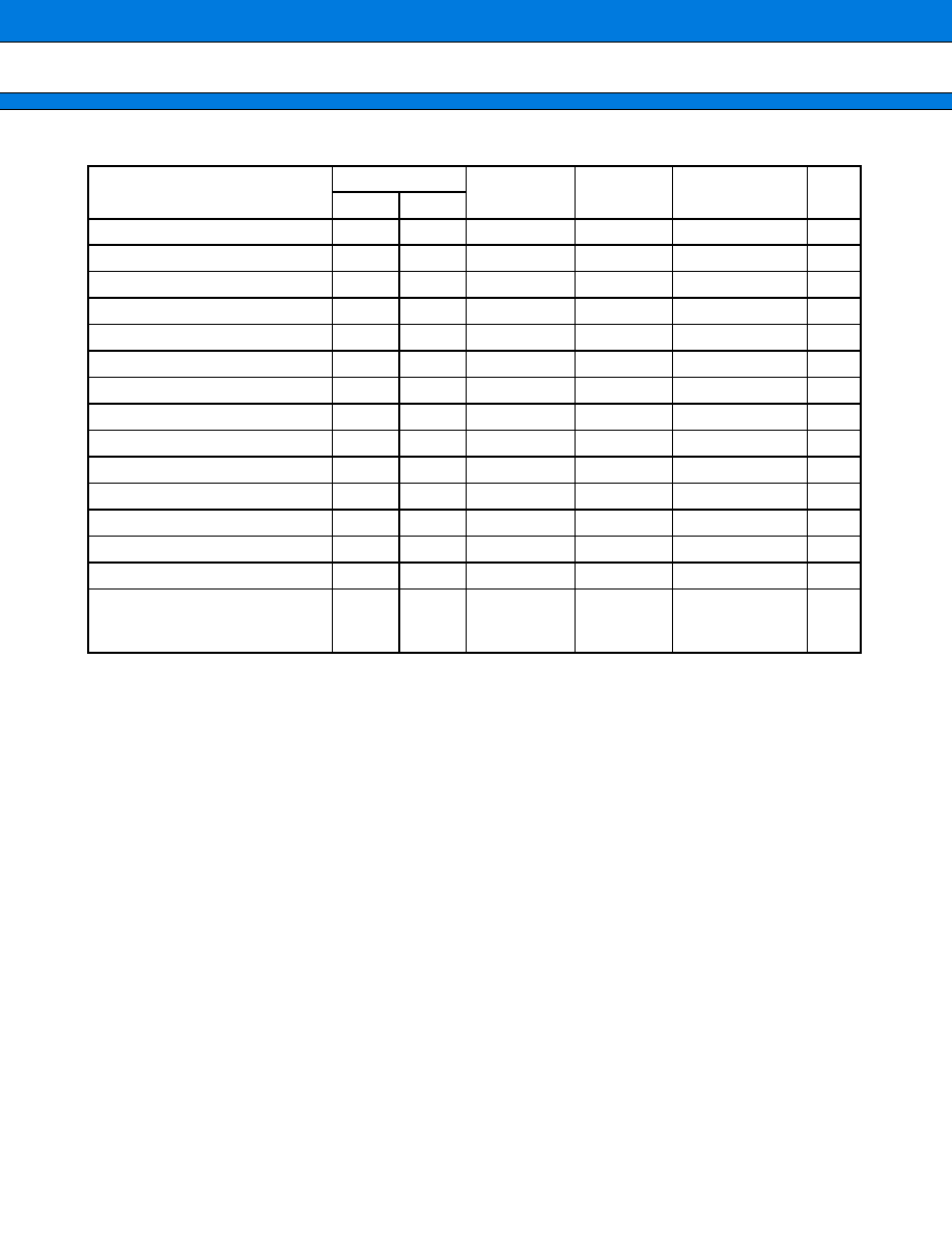
MB91260B Series
37
(Continued)
Interrupt source
Interrupt number
Interrupt
level
Offset
TBR default
address
RN
10
16
System reserved
66
42
2F4
H
000FFEF4
H
System reserved
67
43
2F0
H
000FFEF0
H
System reserved
68
44
2EC
H
000FFEEC
H
System reserved
69
45
2E8
H
000FFEE8
H
System reserved
70
46
2E4
H
000FFEE4
H
System reserved
71
47
2E0
H
000FFEE0
H
System reserved
72
48
2DC
H
000FFEDC
H
System reserved
73
49
2D8
H
000FFED8
H
System reserved
74
4A
2D4
H
000FFED4
H
System reserved
75
4B
2D0
H
000FFED0
H
System reserved
76
4C
2CC
H
000FFECC
H
System reserved
77
4D
2C8
H
000FFEC8
H
System reserved
78
4E
2C4
H
000FFEC4
H
System reserved
79
4F
2C0
H
000FFEC0
H
Used by INT instruction
80
to
255
50
to
FF
2BC
H
to
000
H
000FFEBC
H
to
000FFC00
H

MB91260B Series
38
s
s
s
s
PIN STATUS IN EACH CPU STATE
Terms used as the status of pins mean as follows.
∑ Input enabled
∑ Indicates that the input function can be used.
∑ Input 0 fixed
∑ Indicates that the input level has been internally fixed to be 0 to prevent leakage when the input is released.
∑ Output Hi-Z
∑ Means the placing of a pin in a high impedance state by preventing the transistor for driving the pin from driving.
∑ Output is maintained.
∑ Indicates the output in the output state existing immediately before this mode is established.
∑ If the device enters this mode with an internal output peripheral operating or while serving as an output port,
the output is performed by the internal peripheral or the port output is maintained, respectively.
∑ State existing immediately before is maintained.
∑ When the device serves for output or input immediately before entering this mode, the device maintains the
output or is ready for the input, respectively.
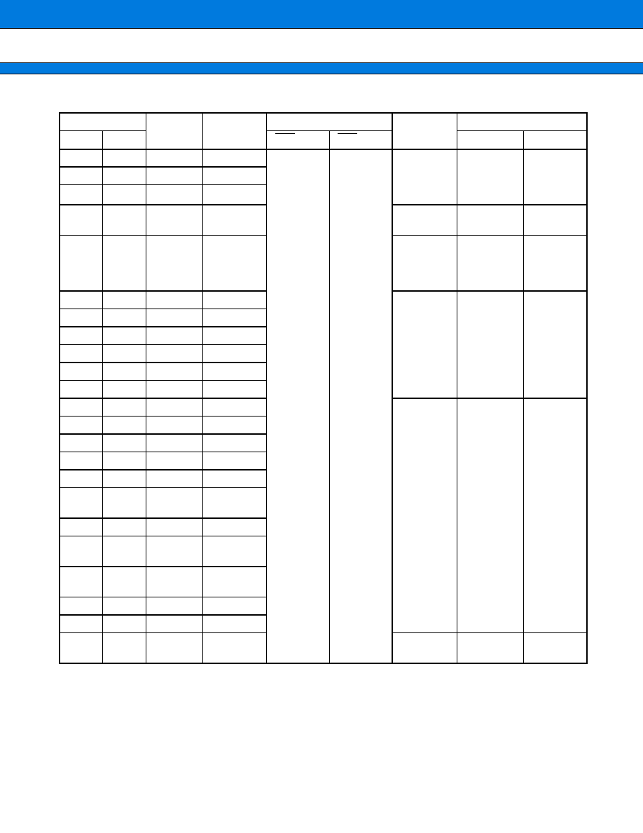
MB91260B Series
39
∑
List of pin status (single chip mode)
(Continued)
Pin no.
Pin name
Function
At initializing
At sleep
mode
At Stop mode
QFP
LQFP
INIT
=
=
=
=
L*
1
INIT
=
=
=
=
H*
2
Hi-Z
=
=
=
=
0
Hi-Z
=
=
=
=
1
1
99
P23
SIN1
Output Hi-Z/
Input
disabled
Output Hi-Z/
Input
disabled
Retention
of the
immediately
prior state
Retention
of the
immediately
prior state
Output Hi-Z/
Input 0 fixed
2
100
P24
SOT1
3
1
P25
SCK1
4, 5
2, 3
P26, P27
INT6, INT7
Input
enabled
Input
enabled
Input
enabled
6 to 9
4 to 7
P50 to P53
Ports
Retention
of the
immediately
prior state
Retention
of the
immediately
prior state
Output Hi-Z/
Input 0 fixed
10
8
P54
INT0
Input
enabled
Input
enabled
Input
enabled
11
9
P55
INT1
12
10
P56
INT2
13
11
P57
INT3
14
12
PG0
CKI/INT4
15
13
PG1
PPG0/INT5
16
14
PG2
Ports
Retention
of the
immediately
prior state
Retention
of the
immediately
prior state
Output Hi-Z/
Input 0 fixed
20
18
PG3
SIN2
21
19
PG4
SOT2
22
20
PG5
SCK2
23 to 30 21 to 28 P40 to P47
Ports
31, 32
29, 30
PE1, PE0
AN11,
AN10
38, 39
36, 37
PD1, PD0
AN9, AN8
41 to 48 39 to 46
PC7 to
PC0
AN7 to AN0
51 to 56 49 to 54 P30 to P35
RTO0 to
RTO5
57, 58
55, 56
P36, P37
IC0, IC1
59, 60
57, 58
P60, P61
IC2, IC3
61, 62
59, 60
P62, P63
INT8, INT9
Input
enabled
Input
enabled
Input
enabled
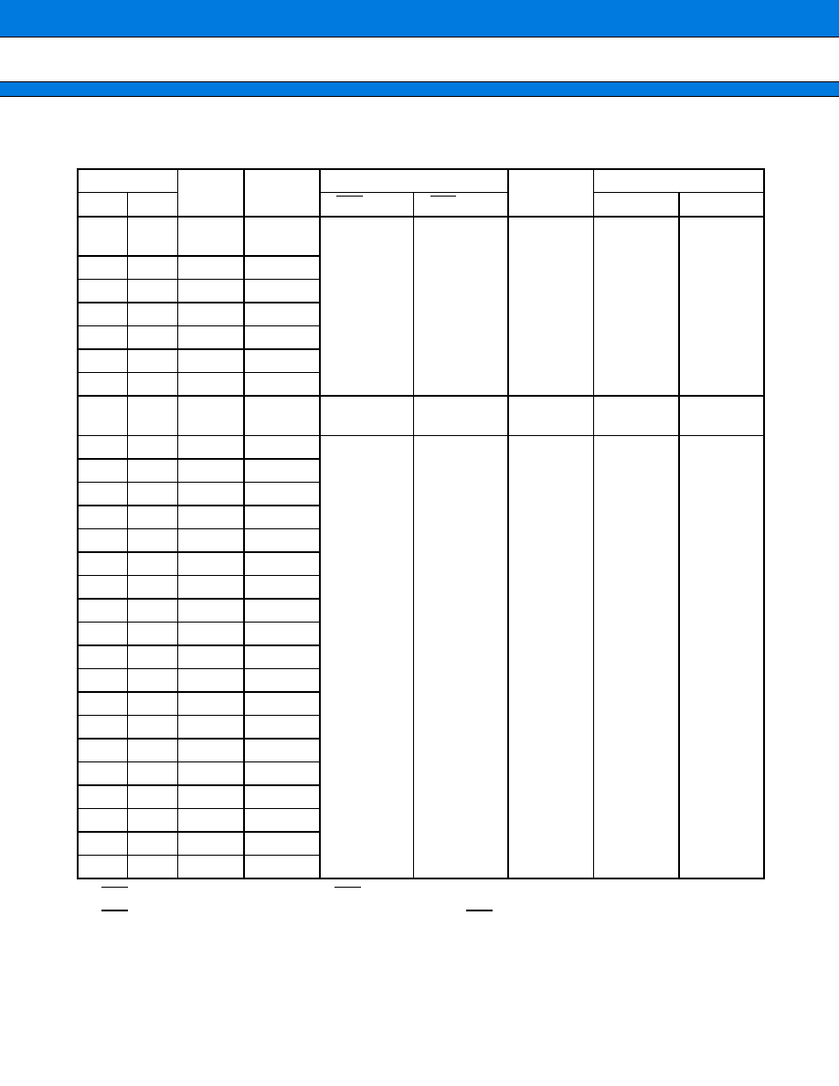
MB91260B Series
40
(Continued)
P : Selection of general purpose port, F : Selection of specified function
*1 : INIT = L : Indicates the pin status with INIT remaining at the "L" level.
*2 : INIT = H : Indicates the pin status existing immediately after INIT transition from "L" to "H" level.
Pin no.
Pin
name
Function
At initializing
At sleep
mode
At Stop mode
QFP
LQFP
INIT
=
=
=
=
L*
1
INIT
=
=
=
=
H*
2
Hi-Z
=
=
=
=
0
Hi-Z
=
=
=
=
1
63, 64 61, 62 P70, P71
TOT1,
TOT2
Output Hi-Z/
input disabled
Output Hi-Z/
input disabled
Retention
of the
immediately
prior state
Retention
of the
immediately
prior state
Output Hi-Z/
Input 0 fixed
65
63
P72
DTTI
66
64
P73
PWI0
69
67
P74
PWI1
70
68
P75
ADTG0
71
69
P76
ADTG1
72
70
P77
ADTG2
73
71
NMI
NMI
Input enabled Input enabled
Input
enabled
Input
enabled
Input
enabled
78
76
P00
PPG1
Output Hi-Z/
input disabled
output Hi-Z/
input disabled
Retention
of the
immediately
prior state
Retention
of the
immediately
prior state
Ouptut Hi-Z/
input 0 fixed
79
77
P01
PPG2
80
78
P02
PPG3
81
79
P03
PPG4
82
80
P04
PPG5
83
81
P05
PPG6
84
82
P06
PPG7
85
83
P07
PPG8
86
84
P10
PPG9
87
85
P11
PPG10
88
86
P12
PPG11
89
87
P13
PPG12
90
88
P14
PPG13
91
89
P15
PPG14
96
94
P16
PPG15
97
95
P17
Ports
98
96
P20
SIN0
99
97
P21
SOT0
100
98
P22
SCK0
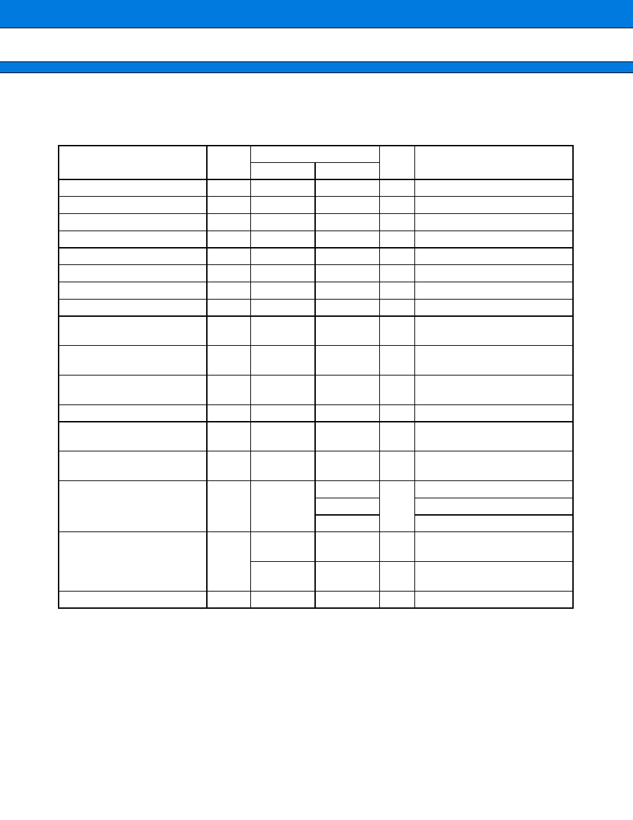
MB91260B Series
41
s
s
s
s
ELECTRICAL CHARACTERISTICS
1.
Absolute Maximum Ratings
(V
SS
=
AV
SS
=
0 V)
*1 : Be careful not to exceed V
CC
+
0.3 V, for example, when the power is turned on.
Be careful not to let AV
CC
exceed V
CC
, for example, when the power is turned on.
*2 : The maximum output current is the peak value for a single pin.
*3 : The average output current is the average current for a single pin over a period of 100 ms.
*4 : The total average output current is the average current for all pins over a period of 100 ms.
*5 : For use at Ta
=
+
105
∞
C, lower the operating frequency to reduce power consumption.
WARNING: Semiconductor devices can be permanently damaged by application of stress (voltage, current,
temperature, etc.) in excess of absolute maximum ratings. Do not exceed these ratings.
Parameter
Symbol
Rating
Unit
Remarks
Min
Max
Power supply voltage
V
CC
V
SS
-
0.5
V
SS
+
6.0
V
Analog power supply voltage
AV
CC
V
SS
-
0.5
V
SS
+
6.0
V
*1
Analog reference voltage
AVRH
V
SS
-
0.5
V
SS
+
6.0
V
*1
Input voltage
V
I
V
SS
-
0.3
V
CC
+
0.3
V
Analog pin input voltage
V
IA
V
SS
-
0.3
AVcc
+
0.3
V
Output voltage
V
O
V
SS
-
0.3
V
CC
+
0.3
V
L level maximum output current
I
OL
10
mA
*2
L level average output current
I
OLAV
8
mA
*3
L level total maximum output
current
I
OL
100
mA
L level total average output
current
I
OLAV
50
mA
*4
H level maximum output
current
I
OH
-
10
mA
*2
H level average output current
I
OHAV
-
4
mA
*3
H level total maximum output
current
I
OH
-
50
mA
H level total average output
current
I
OHAV
-
20
mA
*4
Power consumption
P
D
600
mW
FLASH product
600
MASK product Ta
+
85
∞
C
360
MASK product Ta
+
105
∞
C *
5
Operating temperature
Ta
-
40
+
105
∞
C
MASK product (at single chip
operating)
-
40
+
85
∞
C
FLASH product (at single chip
operating)
Storage temperature
Tstg
-
55
125
∞
C
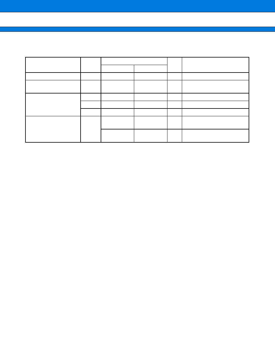
MB91260B Series
42
2.
Recommended Operating Conditions
(Vss
=
AVss
=
0 V)
WARNING: The recommended operating conditions are required in order to ensure the normal operation of the
semiconductor device. All of the device's electrical characteristics are warranted when the device is
operated within these ranges.
Always use semiconductor devices within their recommended operating condition ranges. Operation
outside these ranges may adversely affect reliability and could result in device failure.
No warranty is made with respect to uses, operating conditions, or combinations not represented on
the data sheet. Users considering application outside the listed conditions are advised to contact their
FUJITSU representatives beforehand.
Parameter
Symbol
Value
Unit
Remarks
Min
Max
Power supply voltage
V
CC
4.0
5.5
V
At normal operating
Analog power supply
voltage
AV
CC
V
SS
+
4.0
V
SS
+
5.5
V
Analog reference voltage
AVRH0
AV
SS
AV
CC
V
For A/D converter 0
AVRH1
AV
SS
AV
CC
V
For A/D converter 1
AVRH2
AV
SS
AV
CC
V
For A/D converter 2
Operating temperature
Ta
-
40
+
105
∞
C
MASK product (at single chip
operation)
-
40
+
85
∞
C
FLASH product (at single chip
operation)
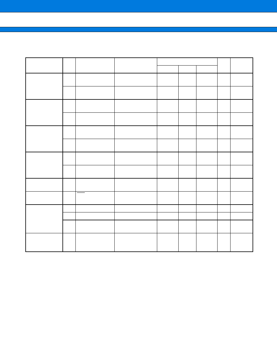
MB91260B Series
43
3.
DC Characteristics
(V
CC
=
4.0 to 5.5 V, V
SS
=
AV
SS
=
0 V)
Parameter
Sym
bol
Pin
Conditions
Value
Unit Remarks
Min
Typ
Max
"H" level input
voltage
V
IH
Other than hyster-
esis input pin
0.8
◊
Vcc
Vcc
V
V
IHS
Hysteresis input
pin
Vcc
-
0.4
Vcc
V
Input Low
Voltage
V
IL
Other than hyster-
esis input pin
Vss
0.2
◊
Vcc
V
V
ILS
Hysteresis input
pin
Vss
Vss
+
0.4
V
"H" level output
voltage
V
OH
Other than port 30
to 35
V
CC
=
5.0 V,
I
OH
=
4.0 mA
Vcc
-
0.5
V
V
OH2
Port 30 to 35
V
CC
=
5.0 V,
I
OH
=
8.0 mA
Vcc
-
0.7
V
Output Low
Voltage
V
OL
Other than port 30
to 35
V
CC
=
5.0 V,
I
OL
=
4.0 mA
0.4
V
V
OL2
Port 30 to 35
V
CC
=
5.0 V,
I
OL
=
12 mA
0.6
V
Input leak current
I
LI
V
CC
=
5.0 V,
V
SS
V
I
V
CC
-
5
5
µ
A
Pullup resistance R
PULL
INIT,
Pull-up pin
50
k
Power supply
current
I
CC
V
CC
V
CC
=
5.0 V, 33 MHz
90
100
mA
I
CCS
V
CC
V
CC
=
5.0 V, 33 MHz
60
80
mA
At SLEEP
I
CCH
V
CC
V
CC
=
5.0 V,
Ta
=
+
25
∞
C
300
µ
A
At STOP
Input
capacitance
C
IN
Other than V
CC
,
V
SS
, AV
CC
, AV
SS
,
AVRH0, 1, 2
10
pF
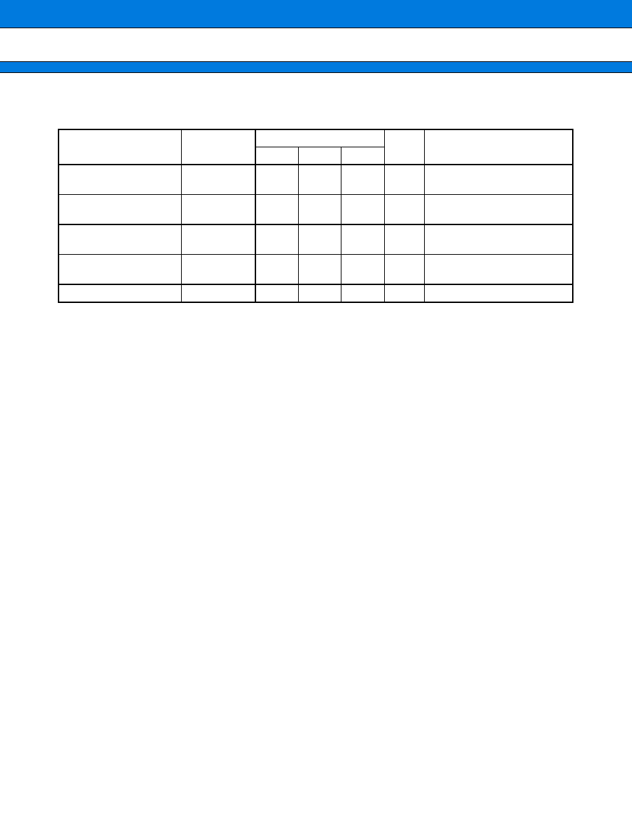
MB91260B Series
44
4.
FLASH MEMORY write/erase characteristics
Parameter
Conditions
Value
Unit
Remarks
Min
Typ
Max
Sector erase time
Ta
=
+
25
∞
C,
Vcc
=
5.0 V
1
15
s
Not including time for internal
writing before deletion.
Chip erase time
Ta
=
+
25
∞
C,
Vcc
=
5.0 V
10
s
Not including time for internal
writing before deletion.
Byte write time
Ta
=
+
25
∞
C,
Vcc
=
5.0 V
8
3,600
µ
s
Not including system-level
overhead time.
Chip write time
Ta
=
+
25
∞
C,
Vcc
=
5.0 V
2.1
s
Not including system-level
overhead time.
Erase/write cycle
10,000
Cycle

MB91260B Series
45
5.
AC Characteristics
(1) Clock Timing Ratings
(V
CC
=
4.0 to 5.5 V, V
SS
=
AV
SS
=
0 V)
* : The values assume a gear cycle of 1/16.
∑
Conditions for measuring the clock timing ratings
Parameter
Sym
bol
Pin
Conditions
Value
Unit
Remarks
Min
Typ
Max
Clock frequency
f
C
X0
X1
3.6
12
MHz
For using the PLL within
the self-oscillation enabled
range, set the multiplier for
the internal clock not to let
the operating frequency
exceed 33 MHz.
Clock cycle time
t
C
X0
X1
83.3
278
ns
Internal operating
clock frequency
f
CP
When 4.125 MHz is
input as the X0
clock frequency and
◊
8 multiplication is
set for the PLL of
the oscillator circuit.
2.06*
33
MHz CPU
f
CPP
2.06*
33
MHz Peripheral
Internal operating
clock cycle time
t
CP
30.3
485*
ns
CPU
t
CPP
30.3
485*
ns
Peripheral
0.8 V
CC
0.2 V
CC
t
CF
t
CR
t
C
P
WH
P
WL
C
=
50 pF
Output pin
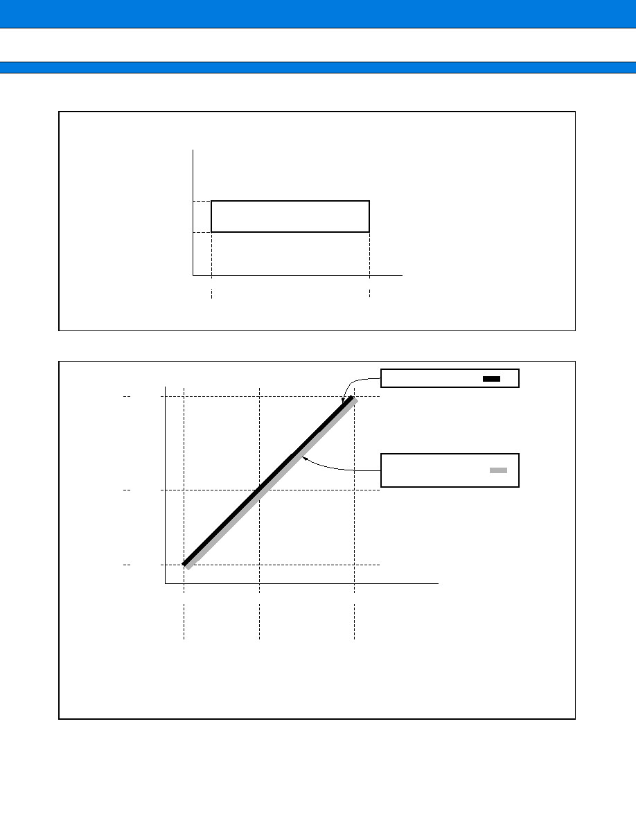
MB91260B Series
46
∑
Operation Assurance Range
∑
Internal clock setting range
0
(MHz)
5.5
4.0
f
CP
/ f
CPP
33
0.25
V
CC
(V)
Internal clock
Power supply
33
(MHz)
16.5
4.125
8 : 8
4 : 4
1 : 1
Notes :
∑
Oscillation stabilization time of PLL
>
600
µ
s
∑
The internal clock gear setting should be within the value shown in clock timing ratings table.
Oscillation input clock f
C
=
4
.
192 MHz
CPU : Divided ratio for
peripherals.
Internal clock
Peripheral (CLKP) :
CPU (CLKB) :
(PLL multiplied by 8)
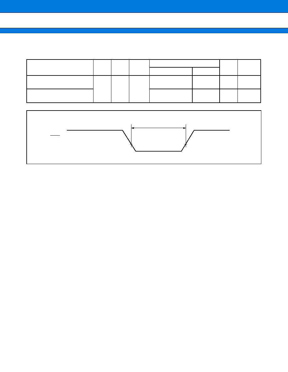
MB91260B Series
47
(2) Reset Input
(V
CC
=
4.0 to 5.5 V, V
SS
=
AV
SS
=
0 V)
Parameter
Sym-
bol
Pin
Condi-
tions
Value
Unit
Remarks
Min
Max
Init input time
(at power-on and STOP mode)
t
INTL
INIT
Oscillation time of
oscillator
+
t
C
◊
10
ns
Init input time
(other than the above)
t
C
◊
10
ns
INIT
0.2 V
CC
t
INTL
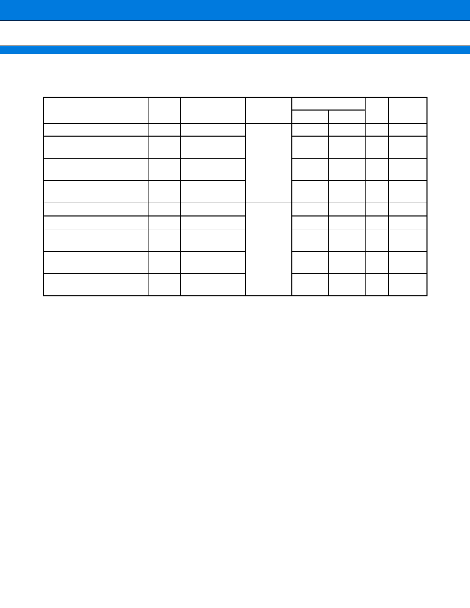
MB91260B Series
48
(3) UART Timing
(V
CC
=
4.0 to 5.5 V, V
SS
=
AV
SS
=
0 V)
Notes :
∑
There are the AC ratings for CLK synchronous mode.
∑
t
CYCP
indicates the peripheral clock cycle time.
Parameter
Symbol
Pin
Conditions
Value
Unit
Remarks
Min
Max
Serial clock cycle time
t
SCYC
SCK0 to SCK2
Internal shift
clock mode
8 t
CYCP
ns
SCK
SOT delay time
t
SLOV
SCK0 to SCK2,
SOT0 to SOT2
-
80
80
ns
Valid SIN
SCK
t
IVSH
SCK0 to SCK2,
SIN0 to SIN2
100
ns
SCK
valid SIN hold time
t
SHIX
SCK0 to SCK2,
SIN0 to SIN2
60
ns
Serial clock H pulse width
t
SHSL
SCK0 to SCK2
External
shift clock
mode
4 t
CYCP
ns
Serial clock L pulse width
t
SLSH
SCK0 to SCK2
4 t
CYCP
ns
SCK
SOT delay time
t
SLOV
SCK0 to SCK2,
SOT0 to SOT2
150
ns
Valid SIN
SCK
t
IVSH
SCK0 to SCK2,
SIN0 to SIN2
60
ns
SCK
valid SIN hold time
t
SHIX
SCK0 to SCK2,
SIN0 to SIN2
60
ns
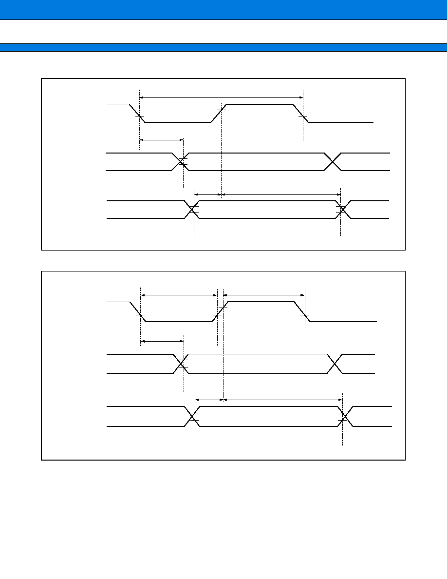
MB91260B Series
49
∑
Internal shift clock mode
∑
External shift clock mode
SCK0 to SCK2
t
SCYC
t
SLOV
t
IVSH
t
SHIX
V
OL
V
OL
V
OH
V
OH
V
OL
V
OH
V
OL
V
OH
V
OL
SOT0 to SOT2
SIN0 to SIN2
t
SLSH
t
SLOV
t
IVSH
t
SHIX
t
SHSL
V
OH
V
OL
V
OH
V
OL
V
OH
V
OL
V
OH
V
OL
V
OL
V
OL
SCK0 to SCK2
SOT0 to SOT2
SIN0 to SIN2
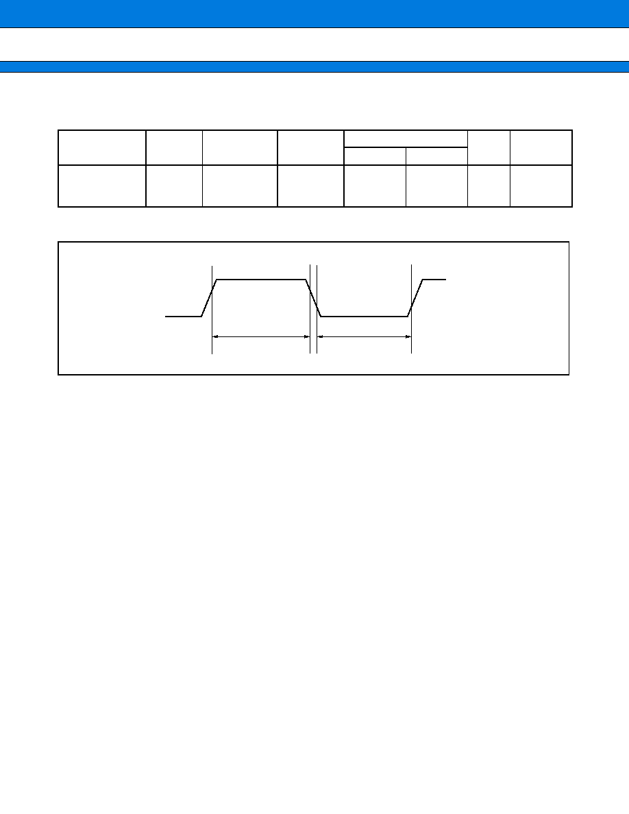
MB91260B Series
50
(4) Free-run Timer Clock, PWC Input and Reload Timer Trigger Timing
(V
CC
=
4.0 to 5.5 V, V
SS
=
AV
SS
=
0 V)
Note : t
CYCP
indicates the peripheral clock cycle time.
Parameter
Symbol
Pin
Conditions
Value
Unit
Remarks
Min
Max
Input pulse width
t
TIWH
t
TIWL
CKI
PWI0, PWI1
TIN0 to TIN2
4 t
CYCP
ns
t
TIWH
t
TIWL
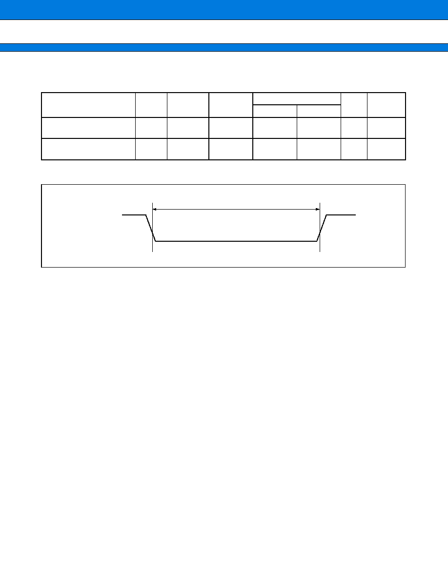
MB91260B Series
51
(5) Trigger Input Timing
(V
CC
=
4.0 to 5.5 V, V
SS
=
AV
SS
=
0 V)
Note : t
CYCP
indicates the peripheral clock cycle time.
Parameter
Symbol
Pin
Conditions
Value
Unit
Remarks
Min
Max
Input capture
trigger input
t
INP
IC0 to IC3
5 t
CYCP
ns
A/D activation trigger input
t
ATGX
ADTG0 to
ADTG2
5 t
CYCP
ns
IC0 to IC3
ADTG0 to ADTG2
t
ATGX
, t
INP
MB91260B Series
52
6.
Electrical Characteristics for the A/D Converter
(V
CC
=
AVcc
=
5.0 V, V
SS
=
AV
SS
=
0 V)
*1 : Measured in the CPU sleep state
*2 : Vcc
=
AVcc
=
5.0 V, machine clock at 33 MHz
*3 : The current when the CPU is in stop mode and the A/D converter is not operating (at Vcc
=
AVcc
=
AVRHn
=
5.0 V)
*4: AVRHn
=
AVRH0, AVRH1, AVRH2
Note : The above does not guarantee the inter-unit accuracy.
Set the output impedance of the external circuit
2 k
.
Parameter
Sym-
bol
Pin
Value
Unit
Remarks
Min
Typ
Max
Resolution
10
bit
Total error*
1
-
4
4
LSB
At AVRHn*
4
=
5.0 V
Linearity error*
-
3.5
3.5
LSB
Differential linearity
error*
1
-
3
3
LSB
Zero transition voltage*
1
V
OT
AN0 to
AN11
AVss
-
3.5 AVss
+
0.5 AVss
+
4.5 LSB
Full transition voltage*
1
V
FST
AN0 to
AN11
AVRH
-
5.5
AVRH
-
1.5
AVRH
+
2.5
LSB
Conversion time
1.2*
2
µ
S
Analog port
Input current
I
AIN
AN0 to
AN11
10
µ
A
Analog input voltage
V
AIN
AN0 to
AN11
AVss
AVRH
V
Reference voltage
AVRHn
AVss
AVcc
V
Analog power supply
current
(analog
+
digital)
I
A
AVcc
2
mA
Per 1 unit
I
AH
*
3
100
µ
A
Per 1 unit
reference power supply
current
(between AVRH and
AVSS)
I
R
AVRHn
1
mA
Per 1 unit
AVRHn*
4
=
5.0 V,
at AVss
=
0 V
I
RH
*
3
100
µ
A
per 1 unit
at STOP
Analog input capacitance
10
pF
Inter-channel disparity
AN0 to
AN11
4
LSB
MB91260B Series
53
Definition of A/D Converter Terms
∑ Resolution : Analog variation that is recognized by an A/D converter.
∑ Linearity error : Zero transition point (00 0000 0000
00 0000 0001) and full-scale transition point.
Difference between the line connected (11 1111 1110
11 1111 1111) and actual conversion character-
istics.
∑ Differential linearity error : Deviation of input voltage, that is required for changing output code by 1 LSB, from
an ideal value.
∑ Total error : This error indicates the difference between actual and ideal values, including the zero transition
error/full-scale transition error/linearity error.
(Continued)
3FF
3FE
3FD
004
003
002
001
AV
SS
AVRH
0.5 LSB'
{1 LSB' (N
-
1)
+
0.5 LSB'}
1.5 LSB'
Digital output
Analog input
Total error
Ideal characteristics
Actual conversion
characteristics
V
NT
(measurement value)
Actual conversion
characteristics
1LSB'
(Ideal value)
=
AVRH
-
AV
SS
[V] Total error of digital output N
=
V
NT
-
{1 LSB'
◊
(N
-
1)
+
0.5 LSB'}
1024
1 LSB'
V
OT
'
(Ideal value)
=
AV
SS
+
0.5 LSB' [V]
V
FST
'
(Ideal value)
=
AVRH
-
1.5 LSB' [V] V
NT
: A voltage at which digital output transitions from (N
+
1) to N.
MB91260B Series
54
(Continued)
3FF
3FE
3FD
004
003
002
001
AV
SS
AVRH
{1 LSB (N
-
1)
+
V
OT
}
N
-
1
AV
SS
AVRH
N
-
2
N
N
+
1
Digital output
Analog input
Linearity error
Ideal characteristics
Actual conversion
characteristics
V
FST
(measurement
value)
Actual conversion
characteris
tics
V
0T
(
measurement
Value)
Digital output
Analog input
Differential linear error
Actual conversion
characteristics
Ideal
characteristics
V
FST
(measurement
value)
V
NT
(measurement value)
V
NT
(measurement value)
Actual conversion
characteristics
V
OT
: A voltage at which digital output transitions from 000
H
to 001
H
.
V
FST
: A voltage at which digital output transitions from 3FE
H
to 3FF
H
.
Linearity error in digital output N
=
VNT
-
{ 1 LSB
◊
(N
-
1)
+
VOT }
[LSB]
1 LSB
Differential linearity error in digital output
N
=
V (
N
+
1
)
T
-
V
NT
-
1
[LSB]
1 LSB
1 LSB
=
V
FST
-
V
OT
[V]
1022
MB91260B Series
55
s
s
s
s
EXAMPLE CHARACTERISTICS
(Continued)
6
5
4
3
2
1
0
4.0
4.5
5.0
5.5
V
CC
(V)
V
OH
(V)
400
350
300
250
200
150
100
50
0
4.0
4.5
5.0
5.5
V
CC
(V)
V
OL
(mV)
80
70
60
50
40
30
20
10
0
4.0
4.5
5.0
5.5
V
CC
(V)
R
(k
)
100
90
80
70
60
50
40
30
20
10
0
4.0
4.5
5.0
5.5
V
CC
(V)
I
CC
(mA)
15
20
25
30
35
100
90
80
70
60
50
40
30
20
10
0
I
CC
(mA)
4.0 V
4.5 V
5.0 V
5.5 V
"H" Level Output Voltage vs.
Power Supply Voltage
"L"
Level Output Voltage vs.
Power Supply Voltage
Pull-up Resistor vs. Power Supply Voltage
Power Supply Current vs. Power Supply Voltage
Power Supply Current vs. Internal Operation Frequency (MB91263)
Internal operation frequency [MHz]
MB91260B Series
56
(Continued)
80
70
60
50
40
30
20
10
0
4.0
4.5
5.0
5.5
V
CC
(V)
I
CCS
(mA)
100
90
80
70
60
50
40
30
20
10
0
4.0
4.5
5.0
V
CC
(V)
I
CCH
(
µ
A)
5.5
2
1.5
1
0.5
0
4.0
4.5
5.0
V
CC
(V)
I
A
(mA)
5.5
1.0
0.8
0.6
0.4
0.2
0.0
4.0
4.5
5.0
V
CC
(V)
I
R
(mA)
5.5
Power Supply Current (at stop) vs.
Power Supply Voltage
A/D Conversion Block Per 1 Unit (33 MHz)
Analog Power Supply Current vs.
Power Supply Voltage
A/D Conversion Block Per 1 Unit (33 MHz)
Reference Voltage Supplying Current vs.
Power Supply Voltage
Power Supply Current (at sleep) vs.
Power Supply Voltageage
MB91260B Series
57
s
s
s
s
ORDERING INFORMATION
Part number
Package
Remarks
MB91F264BPF-G
100-pin plastic QFP
(FPT-100P-M06)
MB91F264BPF-G-E1
Lead-free Package
MB91F264BPFV-G
100-pin plastic LQFP
(FPT-100P-M05)
MB91F264BPFV-G-E1
Lead-free Package
MB91263BPF-G-xxx-BND
100-pin plastic QFP
(FPT-100P-M06)
MB91263BPF-G-xxx-BNDE1
Lead-free Package
MB91263BPFV-G-xxx-BND
100-pin plastic LQFP
(FPT-100P-M05)
MB91263BPFV-G-xxx-BNDE1
Lead-free Package
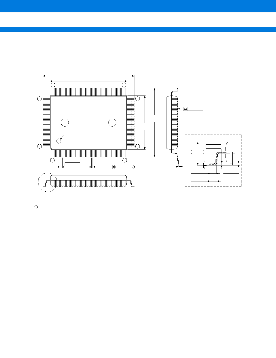
MB91260B Series
58
s
PACKAGE DIMENSION
(Continued)
100 - pin plastic QFP
(FPT-100P-M06)
Note 1) * : These dimensions do not include resin protrusion.
Note 2) Pins width and pins thickness include plating thickness.
Note 3) Pins width do not include tie bar cutting remainder.
Dimensions in mm (inches)
Note: The values in parentheses are reference values.
C
2002 FUJITSU LIMITED F100008S-c-5-5
1
30
31
50
51
80
81
100
20.00±0.20(.787±.008)
23.90±0.40(.941±.016)
14.00±0.20
(.551±.008)
17.90±0.40
(.705±.016)
INDEX
0.65(.026)
0.32±0.05
(.013±.002)
M
0.13(.005)
"A"
0.17±0.06
(.007±.002)
0.10(.004)
Details of "A" part
(.035±.006)
0.88±0.15
(.031±.008)
0.80±0.20
0.25(.010)
3.00
+0.35
≠0.20
+.014
≠.008
.118
(Mounting height)
0.25±0.20
(.010±.008)
(Stand off)
0~8∞
*
*
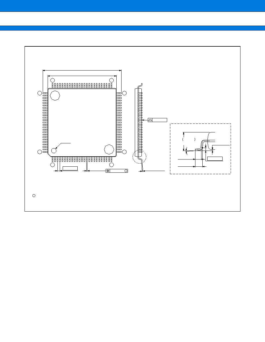
MB91260B Series
59
(Continued)
100-pin plastic LQFP
(FPT-100P-M05)
Note 1) * : These dimensions do not include resin protrusion.
Note 2) Pins width and pins thickness include plating thickness.
Note 3) Pins width do not include tie bar cutting remainder.
Dimensions in mm (inches)
Note: The values in parentheses are reference values.
C
2003 FUJITSU LIMITED F100007S-c-4-6
14.00±0.10(.551±.004)SQ
16.00±0.20(.630±.008)SQ
1
25
26
51
76
50
75
100
0.50(.020)
0.20±0.05
(.008±.002)
M
0.08(.003)
0.145±0.055
(.0057±.0022)
0.08(.003)
"A"
INDEX
.059
≠.004
+.008
≠0.10
+0.20
1.50
(Mounting height)
0∞~8∞
0.50±0.20
(.020±.008)
0.60±0.15
(.024±.006)
0.25(.010)
0.10±0.10
(.004±.004)
Details of "A" part
(Stand off)
*

MB91260B Series
FUJITSU LIMITED
All Rights Reserved.
The contents of this document are subject to change without notice.
Customers are advised to consult with FUJITSU sales
representatives before ordering.
The information, such as descriptions of function and application
circuit examples, in this document are presented solely for the
purpose of reference to show examples of operations and uses of
Fujitsu semiconductor device; Fujitsu does not warrant proper
operation of the device with respect to use based on such
information. When you develop equipment incorporating the
device based on such information, you must assume any
responsibility arising out of such use of the information. Fujitsu
assumes no liability for any damages whatsoever arising out of
the use of the information.
Any information in this document, including descriptions of
function and schematic diagrams, shall not be construed as license
of the use or exercise of any intellectual property right, such as
patent right or copyright, or any other right of Fujitsu or any third
party or does Fujitsu warrant non-infringement of any third-party's
intellectual property right or other right by using such information.
Fujitsu assumes no liability for any infringement of the intellectual
property rights or other rights of third parties which would result
from the use of information contained herein.
The products described in this document are designed, developed
and manufactured as contemplated for general use, including
without limitation, ordinary industrial use, general office use,
personal use, and household use, but are not designed, developed
and manufactured as contemplated (1) for use accompanying fatal
risks or dangers that, unless extremely high safety is secured, could
have a serious effect to the public, and could lead directly to death,
personal injury, severe physical damage or other loss (i.e., nuclear
reaction control in nuclear facility, aircraft flight control, air traffic
control, mass transport control, medical life support system, missile
launch control in weapon system), or (2) for use requiring
extremely high reliability (i.e., submersible repeater and artificial
satellite).
Please note that Fujitsu will not be liable against you and/or any
third party for any claims or damages arising in connection with
above-mentioned uses of the products.
Any semiconductor devices have an inherent chance of failure. You
must protect against injury, damage or loss from such failures by
incorporating safety design measures into your facility and
equipment such as redundancy, fire protection, and prevention of
over-current levels and other abnormal operating conditions.
If any products described in this document represent goods or
technologies subject to certain restrictions on export under the
Foreign Exchange and Foreign Trade Law of Japan, the prior
authorization by Japanese government will be required for export
of those products from Japan.
F0401
©
FUJITSU LIMITED Printed in Japan