 | –≠–ª–µ–∫—Ç—Ä–æ–Ω–Ω—ã–π –∫–æ–º–ø–æ–Ω–µ–Ω—Ç: MB91F355A | –°–∫–∞—á–∞—Ç—å:  PDF PDF  ZIP ZIP |
DS07-16504-3E
FUJITSU SEMICONDUCTOR
DATA SHEET
32-Bit Proprietary Microcontroller
CMOS
FR60 MB91350A Series
MB91F355A/F356B/355A/354A/V350A
DESCRIPTION
The FR families are lines of standard single-chip microcontrollers each based on a 32-bit high-performance RISC
CPU, incorporating a variety of I/O resources and bus control features for embedded control applications which
require high CPU performance for
This FR60 family is based on FR30 and FR40 families and enhanced is bus access. The FR60 family is a line of
single-chip oriented microcontrollers incorporating a wealth of peripheral resources.
The FR60 family is optimized for embedded control applications requiring high processing power of the CPU,
such as DVD player, navigation, high performance Fax machine, and printer controls.
FEATURES
1.
FR CPU
∑ 32-bit RISC, load/store architecture with a five-stage pipeline
∑ Maximum operating frequency: 50 MHz (using the PLL at an oscillation frequency of 12.5 MHz)
∑ 16-bit fixed length instructions (basic instructions), 1 instruction per cycle
∑ Instruction set optimized for embedded applications: Memory-to-memory transfer, bit manipulation, barrel shift
etc.
∑ Instructions adapted for high-level languages: Function entry/exit instructions, multiple-register load/store in-
structions
(Continued)
PACKAGE
I
2
C license
Purchase of Fujitsu I
2
C components conveys a license under the Philips I
2
C Patent Rights to use, these components in an I
2
C system
provided that the system conforms to the I
2
C Standard Specification as defined by Philips.
176-pin plastic LQFP
(FPT-176P-M02)
MB91350A Series
2
∑ Register interlock functions: Facilitating coding in assemblers
∑ On-chip multiplier supported at the instruction level.
Signed 32-bit multiplication: 5 cycles.
Signed 16-bit multiplication: 3 cycles
∑ Interrupt (PC, PS save): 6 cycles, 16 priority levels
∑ Harvard architecture allowing program access and data access to be executed simultaneously
∑ FR family instruction compatible
2.
Bus Interface
∑ Maximum operating frequency: 25 MHz
∑ Capable of up to 24-bit address full output (16 MB of space)
∑ 8,16-bit data output
∑ Built-in pre-fetch buffer
∑ Non-used data and address pin are usable as general I/O port.
∑ Capable of chip-select signal output for completely independent four areas settable in 64 KB minimum
∑ Support for various memory interfaces:
SRAM, ROM/Flash,
page mode Flash ROM, page mode ROM
∑ Basic bus cycle: 2 cycles
∑ Programmable automatic wait cycle generator capable of inserting wait cycles for each area
∑ RDY input for external wait cycles
∑ Support for fly-by transfer for DMA, which enables wait control of independent I/O
3.
Mounted Memory
4.
DMAC (DMA Controller)
∑ Capable of simultaneous operation of up to 5 channels (3 channels for external
external operation)
∑ Three transfer sources (external pin, internal peripheral, software) selectable by software. (Transfer can be
started from UART0/1/2.)
∑ Addressing using 32-bit full addressing mode (increment, decrement, fixed)
∑ Transfer modes (demand transfer, burst transfer, step transfer, block transfer)
∑ Support for fly-by transfer (between external I/O and memory)
∑ Selectable transfer data size: 8, 16, or 32-bit
∑ Multi-byte transfer enabled (by software)
∑ DMAC descriptor in IO areas (200
H
to 240
H
, 1000
H
to 1024
H
)
5.
Bit Search Module (for REALOS)
∑ Search for the position of the bit 1/0-changed first in 1 word from the MSB
6.
Various Timers
∑ 4 channels of 16-bit reload timer (including 1 channel for REALOS):
Internal clock frequency selectable from among divisions by 2/8/32 (division by 64/128 selectable only for ch3)
∑ 16-bit free-running timer: 1 channel.
Output compare module: 8 channels. Input capture module: 4 channels
∑ 16-bit PPG timer 6 channels
7.
UART
∑ UART Full duplex double buffer 5 channel
∑ Selectable parity On/Off
∑ Asynchronous (start-stop synchronized) or CLK-synchronous communications selectable
(Continued)
Memory
MB91V350A
MB91F355A
MB91F356B
MB91355A
MB91354A
ROM
No
512 KB
256 KB
512 KB
384 KB
RAM (stack)
16 KB
16 KB
16 KB
16 KB
8 KB
RAM (executable)
16 KB
8 KB
8 KB
8 KB
8 KB

MB91350A Series
3
(Continued)
∑ Internal timer for dedicated baud rate
∑ External clock can be used as transfer clock
∑ Assorted error detection functions (for parity, frame, and overrun errors)
∑ 115 Kbps support
8.
SIO
∑ 3 channels for 8-bit data serial transfer
∑ Shift clock selectable from among internal three and external one
∑ Shift direction selectable (transfer from LSB or MSB) selectable
9.
Interrupt Controller
∑ Total of 17 external interrupt lines (1 nonmaskable interrupt pin and 16 normal interrupt pins available for Wake
Up from STOP)
∑ interrupt from internal peripheral
∑ Programmable priorities (16 levels) for all interrupts except the non-maskable interrupt
10. D/A Converter
∑ 8-bit resolution. 3 channels
11. A/D Converter
∑ 10-bit resolution. 12 channels
∑ Casting time for serial/parallel conversion: 1.48
µ
s
∑ Conversion mode (single conversion mode, continuous conversion mode)
∑ Activation source (software, external trigger, peripheral interrupt)
12. Other Interval Timer/Counter
∑ 8/16-bit up/down counter
∑ 16-bit PPG timer 5 channels
∑ Watch dog timer
13.
I
2
C
Bus Interface (400 Kbps supported)
∑ 1channel master/slave sending and receiving
∑ Arbitration and clock synchronization
14. I/O Port
∑ 3 V I/O ports (16 ports shared for external interrupts support 5 V input.)
∑ Max 126 ports
15. Other Features
∑ Internal oscillator circuit as clock source, allowing PLL multiplication to be selected
∑ Provided with INIT as a reset pin (The CPU operates without oscillation stabilization wait interval when the
INIT pin is reset.)
∑ others, watch-dog timer reset, software reset enable
∑ Support for stop and sleep modes for low power consumption, capable of saving power during CPU operation
at 32 kHz.
∑ Gear function
∑ Built-in time base timer
∑ Package: LQFP-176 (lead pitch: 0.50 mm)
∑ CMOS technology(0.35
µ
m)
∑ Power supply voltage: 3.3 V
±
0.3 V
MB91350A Series
4
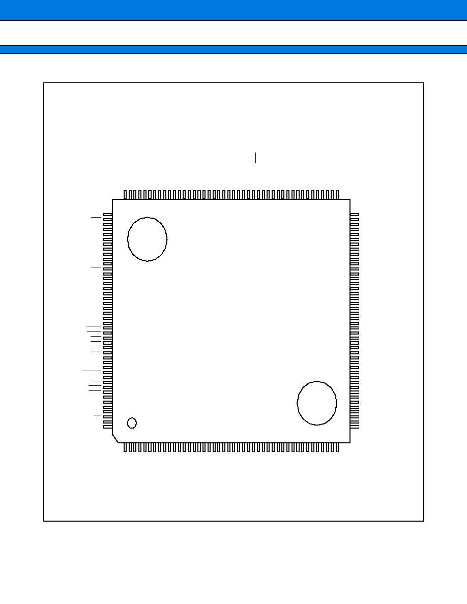
PIN ASSIGNMENT
(TOP VIEW)
(FPT-176P-M02)
133
134
135
136
137
138
139
140
141
142
143
144
145
146
147
148
149
150
151
152
153
154
155
156
157
158
159
160
161
162
163
164
165
166
167
168
169
170
171
172
173
174
175
176
PG5/SCK5
NMI
X1A
V
SS
X0A
MD2
MD1
MD0
X0
V
CC
X1
INIT
V
SS
V
CC
PC0/DREQ2
PC1/DACK2
PC2/DSTP2/DEOP2
PB0/DREQ0
PB1/DACK0
PB2/DSTP0/DEOP0
PB3/DREQ1
PB4/DACK1
PB5/DSTP1/DEOP1
PB6/IOWR
PB7/IORD
PA0/CS0
PA1/CS1
PA2/CS2
PA3/CS3
V
SS
V
CC
P80/IN0/RDY
P81/IN1/BGRNT
P82/IN2/BRQ
P83/RD
P84/WR0
P85/IN3/WR1
P90/SYSCLK
P91
P92/MCLK
P93
P94/AS
V
SS
V
CC
1
2
3
4
5
6
7
8
9
10
11
12
13
14
15
16
17
18
19
20
21
22
23
24
25
26
27
28
29
30
31
32
33
34
35
36
37
38
39
40
41
42
43
44
P
20/D16
P
21/D17
P
22/D18
P
23/D19
P
24/D20
P
25/D21
P
26/D22
P
27/D23
P
30/D24
P
31/D25
P
32/D26
P
33/D27
P
34/D28
P
35/D29
P
36/D30
P
37/D31
V
SS
V
CC
P40/A00
P41/A01
P42/A02
P43/A03
P44/A04
P45/A05
P46/A06
P47/A07
P50/A08
P51/A09
P52/A10
P53/A11
P54/A12
P55/A13
P56/A14
P57/A15
V
SS
V
CC
P60/A16
P61/A17
P62/A18
P63/A19
P64/A20
P65/A21
P66/A22
P67/A23
PG4/SO5
PG3/SI5
PG2/SCK4
PG1/SO4
PG0/SI4
PH5/SCK3
PH4/SO3
PH3/SI3
PH2/SCK2
PH1/SO2
PH0/SI2
PI5/SCK1
PI4/SO1
PI3/SI1
PI2/SCK0
PI1/SO0
PI0/SI0
V
CC
V
SS
PJ7/INT15
PJ6/INT14
PJ5/INT13
PJ4/INT12
PJ3/INT11
PJ2/INT10
PJ1/INT9
PJ0/INT8
PK7/INT7/ATG
PK6/INT6/FRCK
PK5/INT5
PK4/INT4
PK3/INT3
PK2/INT2
PK1/INT1
PK0/INT0
V
CC
V
SS
PL1/SCL
PL0/SDA
VSS
PM5/SCK7/ZIN1/TRG
5
PM4/SO7/BIN1/TRG4
PM3/SI7/AIN1/TRG3
PM2/SCK6/ZIN0/TRG
2
132
131
130
129
128
127
126
125
124
123
122
121
120
119
118
117
116
115
114
113
112
111
110
109
108
107
106
105
104
103
102
101
100
99
98
97
96
95
94
93
92
91
90
89
PM1/SO6/BIN0/TRG1
PM0/SI6/AIN0/TRG0
PN5/PPG5
PN4/PPG4
PN3/PPG3
PN2/PPG2
PN1/PPG1
PN0/PPG0
V
CC
V
SS
PO7/OC7
PO6/OC6
PO5/OC5
PO4/OC4
PO3/OC3
PO2/OC2
PO1/OC1
PO0/OC0
PP3/TOT3
PP2/TOT2
PP1/TOT1
PP0/TOT0
V
CC
V
SS
AV
SS
/AVRL
AVRH
AV
CC
AN11
AN10
AN9
AN8
AN7
AN6
AN5
AN4
AN3
AN2
AN1
AN0
DA2
DA1
DA0
DA
VC
DA
VS
88
87
86
85
84
83
82
81
80
79
78
77
76
75
74
73
72
71
70
69
68
67
66
65
64
63
62
61
60
59
58
57
56
55
54
53
52
51
50
49
48
47
46
45
MB91350A Series
5
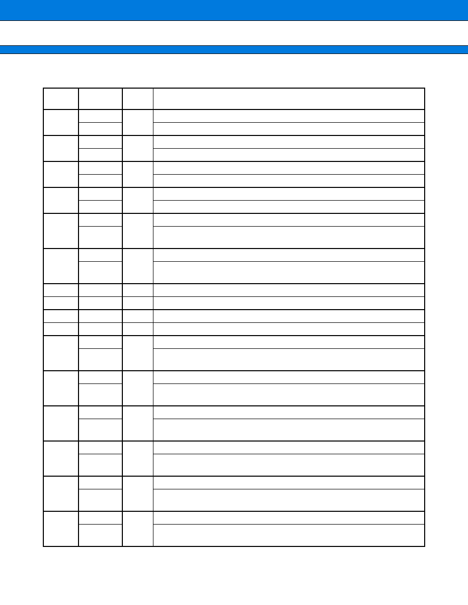
PIN DESCRIPTION
(Continued)
Pin no.
Pin name
Circuit
type
Description
1 to 8
D16 to D23
C
External data bus bit 16 to bit 23. Enabled in external bus mode.
P20 to P27
Available as a port in external bus 8-bit mode.
9 to 16
D24 to D31
C
external data bus bit 24 to bit 31. Enabled in external bus mode.
P30 to P37
Usable as port at single chip mode.
19 to 26
A00 to A07
C
Bits 0 to 7 of external address bus. Enabled in external bus mode.
P40 to P47
Usable as port at single chip mode.
27 to 34
A08 to A15
C
Bits 8 to 15 of external address bus. Enabled in external bus mode.
P50 to P57
Usable as port at single chip mode.
37 to 41
A16 to A20
C
Bits 16 to 20 of external address bus. Enabled in external bus mode.
P60 to P64
Available as a port either in single chip mode or with no external address bus in
use.
42 to 44
A21 to A23
C
Bits 21 to 23 of external address bus. Enabled in external bus mode.
P65 to P67
Available as a port either in single chip mode or with no external address bus in
use.
47 to 48
DA0, DA1
D/A converter output pin.
49
DA2
D/A converter output pin.
50 to 57 AN0 to AN7
G
Analog input pin.
58 to 61
AN8 to AN11
G
Analog input pin.
67 to 70
TOT0 to TOT3
D
Reload timer output port. This function is enabled when timer output is enabled.
PP0 to PP3
General purpose input/output port. This function is enabled when the timer out-
put function is disabled.
71
OC0
D
Output compare pin.
PO0
General purpose I/O. This function is available as a port when the output com-
pare output is not in use.
72
OC1
D
Output compare pin.
PO1
General purpose I/O. This function is available as a port when the output com-
pare output is not in use.
73
OC2
D
Output compare pin.
PO2
General purpose I/O. This function is available as a port when the output com-
pare output is not in use.
74 to 78
OC3 to OC7
D
Output compare pin.
PO3 to PO7
General purpose I/O. This function is available as a port when the output com-
pare output is not in use.
81
PPG0
D
PPG timer output pin.
PN0
General purpose I/O. This function is available as a port when the PPG timer out-
put is not in use.
MB91350A Series
6
(Continued)
Pin no.
Pin name
Circuit
type
Description
82
PPG1
D
PPG timer output pin.
PN1
General purpose I/O. This function is available as a port when the PPG timer out-
put is not in use.
83
PPG2
D
PPG timer output pin.
PN2
General purpose I/O. This function is available as a port when the PPG timer out-
put is not in use.
84
PPG3
D
PPG timer output pin.
PN3
General purpose I/O. This function is available as a port when the PPG timer out-
put is not in use.
85
PPG4
D
PPG timer output pin.
PN4
General purpose I/O. This function is available as a port when the PPG timer out-
put is not in use.
86
PPG5
D
PPG timer output pin.
PN5
General purpose I/O. This function is available as a port when the PPG timer out-
put is not in use.
87
SI6
D
Data input for serial I/O6. Since this input is used as required when serial I/O 6 is
in input operation, the port output must remain off unless intentionally turned on.
AIN0
8/16-bit up/down counter input. Since this input is used as required when en-
abled, the port output must remain off unless intentionally turned on.
TRG0
External trigger input for PPG timer0. Since this input is used as required when
enabled, the port output must remain off unless intentionally turned on.
PM0
General purpose I/O. This function is available a port when the serial I/O, 8/16-
bit up/down counter, and PPG timer outputs are not in use.
88
SO6
D
Data output for serial I/O 6. This function is enabled when the serial I/O6 data out-
put is enabled.
BIN0
8/16-bit up/down counter input. Since this input is used as required when en-
abled, the port output must remain off unless intentionally turned on.
TRG1
External trigger input for PPG timer1. Since this input is used as required when
enabled, the port output must remain off unless intentionally turned on.
PM1
General purpose I/O. This function is available a port when the serial I/O, 8/16-
bit up/down counter, and PPG timer outputs are not in use.
89
SCK6
D
Clock input/output for serial I/O 6. This function is enabled when serial I/O6 is us-
ing the external shift clock mode, or serial I/O5 clock output function is enabled.
ZIN0
8/16-bit up/down counter input. Since this input is used as required when en-
abled, the port output must remain off unless intentionally turned on.
TRG2
External trigger input for PPG timer2. Since this input is used as required when
enabled, the port output must remain off unless intentionally turned on.
PM2
General purpose I/O. This function is available a port when the serial I/O, 8/16-
bit up/down counter, and PPG timer outputs are not in use.
MB91350A Series
7
(Continued)
Pin no.
Pin name
Circuit
type
Description
90
SI7
D
Data input for serial I/O 7. Since this input is used as required when serial I/O 7
is in input operation, the port output must remain off unless intentionally turned
on.
AIN1
8/16-bit up/down counter input. Since this input is used as required when en-
abled, the port output must remain off unless intentionally turned on.
TRG3
External trigger input for PPG timer 3. Since this input is used as required when
enabled, the port output must remain off unless intentionally turned on.
PM3
General purpose I/O. This function is available a port when the serial I/O, 8/16-
bit up/down counter, and PPG timer outputs are not in use.
91
SO7
D
Data output for serial I/O 7. This function is enabled when the serial I/O 7 data
output is enabled.
BIN1
8/16-bit up/down counter input. Since this input is used as required when en-
abled, the port output must remain off unless intentionally turned on.
TRG4
External trigger input for PPG timer 4. Since this input is used as required when
enabled, the port output must remain off unless intentionally turned on.
PM4
General purpose I/O. This function is available a port when the serial I/O, 8/16-
bit up/down counter, and PPG timer outputs are not in use.
92
SCK7
D
Clock input/output for serial I/O5. This function is enabled when serial I/O 7 is us-
ing the external shift clock mode, or serial I/O 5 clock output function is enabled.
ZIN1
8/16-bit up/down counter input. Since this input is used as required when en-
abled, the port output must remain off unless intentionally turned on.
TRG5
External trigger input for PPG timer 5. Since this input is used as required when
enabled, the port output must remain off unless intentionally turned on.
PM5
General purpose I/O. This function is available a port when the serial I/O, 8/16-
bit up/down counter, and PPG timer outputs are not in use.
94
SDA
F
Clock input/output pin for I
2
C bus. This function is enabled when the I
2
C system
is enabled for operation in standard mode. The port output must remain off unless
intentionally turned on. (Open drain input)
PL0
General purpose input/output port. This function is available as a port when the
I
2
C system is disabled for operation. (Open drain input)
95
SCL
F
Clock input/output pin for I
2
C bus. This function is enabled when the I
2
C system
is enabled for operation in standard mode. The port output must remain off unless
intentionally turned on. (Open drain input)
PL1
General purpose input/output port. This function is available as a port when the
I
2
C system is disabled for operation. (Open drain input)
98 to 103
INT0 to
INT5
E
External interrupt input. Since this input is used as required when the correspond-
ing external interrupt is enabled, the port output must remain off unless intention-
ally turned on.
PK0 to PK5
General purpose input/output port.
MB91350A Series
8
(Continued)
Pin no.
Pin name
Circuit
type
Description
104
INT6
E
External interrupt input. Since this input is used as required when the correspond-
ing external interrupt is enabled, the port output must remain off unless intention-
ally turned on.
FRCK
External clock input pin for freerun timer. Since this input is used as required
when selected as the external clock input for the free running timer, the port out-
put must remain off unless intentionally turned on.
PK6
General purpose input/output port.
105
INT7
E
External interrupt input. Since this input is used as required when the correspond-
ing external interrupt is enabled, the port output must remain off unless intention-
ally turned on.
ATG
External trigger input for A/D converter. Since this input is used as required when
selected as an A/D activation source, the port output must remain off unless in-
tentionally turned on.
PK7
General purpose input/output port.
106 to
113
INT8 to
INT15
E
External interrupt input. Since this input is used as required when the correspond-
ing external interrupt is enabled, the port output must remain off unless intention-
ally turned on.
PJ0 to PJ7
General purpose input/output port.
116
SI0
D
UART0 data input. Since this input is used as required when UART0 is in input
operation, the port output must remain off unless intentionally turned on.
PI0
General purpose input/output port.
117
SO0
D
UART0 data output. This function is enabled when the UART0 data output is en-
abled.
PI1
General purpose input/output port. This function is enabled when the data output
function of UART0 is disabled.
118
SCK0
D
UART0 clock input/output pin. This function is enabled either when clock output
enabled or when UART0 inputs the external clock signal.
PI2
General purpose input/output port. This function is enabled when UART0 is not
using the external clock signal with the UART0 clock output function disabled.
119
SI1
D
UART1 data input. Since this input is used as required when UART1 is in input
operation, the port output must remain off unless intentionally turned on.
PI3
General purpose input/output port.
120
SO1
D
UART1 data outpu. This function is enabled when the UART1 data output is en-
abled.
PI4
General purpose input/output port. This function is enabled when the data output
function of UART1 is disabled.
121
SCK1
D
UART1 clock input/output pin. This function is enabled either when clock output
enabled or when UART1 inputs the external clock signal.
PI5
General purpose input/output port. This function is enabled when UART1 is not
using the external clock signal with the UART1 clock output function disabled.
MB91350A Series
9
(Continued)
Pin no.
Pin name
Circuit
type
Description
122
SI2
D
UART2 data input. Since this input is used as required when UART2 is in input
operation, the port output must remain off unless intentionally turned on.
PH0
General purpose input/output port.
123
SO2
D
UART2 data outpu. This function is enabled when the UART2 data output is en-
abled.
PH1
General purpose input/output port. This function is enabled when the data output
function of UART2 is disabled.
124
SCK2
D
UART2 clock input/output pin. This function is enabled either when the UART2
clock output is enabled or when UART2 inputs the external clock signal.
PH2
General purpose input/output port. This function is enabled when UART2 is not
using the external clock signal with the UART2 clock output function disabled.
125
SI3
D
UART3 data input. Since this input is used as required when UART3 is in input
operation, the port output must remain off unless intentionally turned on.
PH3
General purpose input/output port.
126
SO3
D
UART3 data outpu. This function is enabled when the UART3 data output is en-
abled.
PH4
General purpose input/output port. This function is enabled when the data output
function of UART3 is disabled.
127
SCK3
D
UART0 clock input/output pin. This function is enabled either when the UART3
clock output is enabled or when UART3 inputs the external clock signal.
PH5
General purpose input/output port. This function is enabled when UART3 is not
using the external clock signal with the UART3 clock output function disabled.
128
SI4
D
UART4 data input. Since this input is used as required when UART4 is in input
operation, the port output must remain off unless intentionally turned on.
PG0
General purpose input/output port.
129
SO4
D
UART4 data output. This function is enabled when the UART4 data output is en-
abled.
PG1
General purpose input/output port. This function is enabled when the data output
function of UART4 is disabled.
130
SCK4
D
UART4 clock input/output pin. This function is enabled either when the UART4
clock output is enabled or when UART4 inputs the external clock signal.
PG2
General purpose input/output port. This function is enabled when UART4 is not
using the external clock signal with the UART4 clock output function disabled.
131
SI5
D
Data input for serial I/O5. Since this input is used as required when serial I/O5 is
in input operation, the port output must remain off unless intentionally turned on.
PG3
General purpose input/output port.
132
SO5
D
Data output for serial I/O5. This function is enabled when the serial I/O5 data out-
put is enabled.
PG4
General purpose input/output port. This function is enabled when the I/O5 data
output function is disabled.
MB91350A Series
10
(Continued)
Pin no.
Pin name
Circuit
type
Description
133
SCK5
D
Clock innput/output for serial I/O5. This function is enabled when serial I/O5 is
using the external shift clock mode, or serial I/O5 clock output function is en-
abled.
PG5
General purpose input/output port. This function is enabled when serial I/O5 is
not using the external shift clock mode with the serial I/O5 clock output function
disabled.
134
NMI
H
NMI (Non Maskable Interrupt) input
135
X1A
B
Output clock cycle time. Sub clock
137
X0A
B
Input clock cycle time. Sub clock
138 to
140
MD2 to
MD0
H, J
2 to 0Mode Pins. The levels applied to these pins set the basic operating mode.
Connect VCC or VSS.
Input circuit configuration:
The production model (masked-ROM model) is type "H".
The Flash ROM model is type "J".
141
X0
A
Input clock cycle time. Main clock
143
X1
A
Output clock cycle time. Main clock
144
INIT
I
External reset input
147
DREQ2
C
External input for DMA transfer requests. Since this input is used as required
when selected as a DMA start source, the port output must remain off unless in-
tentionally turned on.
PC0
General purpose input/output port.
148
DACK2
C
External acknowledge output for DMA transfer requests. This function is enabled
when the transfer request acceptance output for DMA is enabled.
PC1
General purpose input/output port. This function is enabled when the transfer re-
quest acceptance output for DMA is enabled.
149
DEOP2
C
Completion output for DMA external transfer. This function is enabled when the
external transfer end output for DMA is enabled.
DSTP2
Stop input for DMA external transfer. This function is enabled when the external
transfer stop input for DMA is enabled.
PC2
General purpose input/output port. This function is enabled when the external
transfer end output and external transfer stop input for DMA are disabled.
150
DREQ0
C
External input for DMA transfer requests. Since this input is used as required
when selected as a DMA start source, the port output must remain off unless in-
tentionally turned on.
PB0
General purpose input/output port.
151
DACK0
C
External acknowledge output for DMA transfer requests. This function is enabled
when the transfer request acceptance output for DMA is enabled.
PB1
General purpose input/output port. This function is enabled when the transfer re-
quest acceptance output for DMA is disabled.
MB91350A Series
11
(Continued)
Pin no.
Pin name
Circuit
type
Description
152
DEOP0
C
Completion output for DMA external transfer. This function is enabled when the
external transfer end output for DMA is enabled.
DSTP0
Stop input for DMA external transfer. This function is enabled when the external
transfer stop input for DMA is enabled.
PB2
General purpose input/output port. This function is enabled when the external
transfer end output and external transfer stop input for DMA are disabled.
153
DREQ1
C
External input for DMA transfer requests. Since this input is used as required
when selected as a DMA start source, the port output must remain off unless in-
tentionally turned on.
PB3
General purpose input/output port.
154
DACK1
C
External acknowledge output for DMA transfer requests. This function is enabled
when the transfer request acceptance output for DMA is enabled.
PB4
General purpose input/output port. This function is enabled when the external
transfer request acceptance output for DMA is disabled.
155
DEOP1
C
Completion output for DMA external transfer. This function is enabled when the
external transfer end output for DMA is enabled.
DSTP1
Stop input for DMA external transfer. This function is enabled when the external
transfer stop input for DMA is enabled.
PB5
General purpose input/output port. This function is enabled when the external
transfer end output and external transfer stop input for DMA are disabled.
156
IOWR
C
Write strobe output for DMA fly-by transfer. This function is enabled when the
DMA fly-by transfer write strobe output is enabled.
PB6
General purpose input/output port. This function is enabled when the DMA fly-by
transfer write strobe output is disabled.
157
IORD
C
Read storobe output for DMA fly-by transfer. This function is enabled when the
DMA fly-by transfer read strobe output is enabled.
PB7
General purpose input/output port. This function is enabled when the DMA fly-by
transfer read strobe output is disabled.
158
CS0
C
Chip select 0 output. Enable at external bus mode
PA0
General purpose input/output port. This is enabled at single chip mode.
159
CS1
C
Chip select 1 output. This function is enabled when the chip select 1 output is en-
abled.
PA1
General purpose input/output port. This function is enabled when the chip select
1 output is disabled.
160
CS2
C
Chip select 2 output. This function is enabled when the chip select 2 output is en-
abled.
PA2
General purpose input/output port. This function is enabled when the chip select
2 output is disabled.
MB91350A Series
12
(Continued)
Pin no.
Pin name
Circuit
type
Description
161
CS3
C
Chip select 3 output. This function is enabled when the chip select 3 output is en-
abled.
PA3
General purpose input/output port. This function is enabled when the chip select
3 output is disabled.
164
RDY
D
External ready input. The pin has this function when external ready input is en-
abled.
IN0
Input capture input pin. Since this input is used as required when selected as an
input capture input, the port output must remain off unless intentionally turned on.
P80
General purpose input/output port. This function is enabled when external ready
signal input is disabled.
165
BGRNT
D
Acknowledge output for external bus release. Outputs "L" when the external bus
is released. The pin has this function when output is enabled.
IN1
Input capture input pin. Since this input is used as required when selected as an
input capture input, the port output must remain off unless intentionally turned on.
P81
General purpose input/output port. This function is enabled when external bus re-
lease acknowledge output is disabled.
166
BRQ
D
External bus release request input. Input "1" to request release of the external
bus. The pin has this function when input is enabled.
IN2
Input capture input pin. Since this input is used as required when selected as an
input capture input, the port output must remain off unless intentionally turned on.
P82
General purpose input/output port. The pin has this function when the external
bus release request input is disabled.
167
RD
D
External bus read strobe output. It is available in the external bus mode.
P83
General purpose input/output port. This is enabled at single chip mode.
168
WR0
D
External bus write strobe output. It is available in the external bus mode.
P84
General purpose input/output port. This is enabled at single chip mode.
169
WR1
D
External bus write strobe output. This function is enabled when WR1 output is en-
abled in external bus mode.
IN3
Input capture input pin. Since this input is used as required when selected as an
input capture input, the port output must remain off unless intentionally turned on.
P85
General purpose input/output port. The pin has this function when the external
bus write-enable output is disabled.
170
SYSCLK
C
System clock output The pin has this function when system clock output is en-
abled. This outputs the same clock as the external bus operating frequency. (Out-
put halts in stop mode.)
P90
General purpose input/output port. The pin has this function when system clock
output is disabled.
171
P91
C
General purpose input/output port.
MB91350A Series
13
(Continued)
∑
Power supply and GND pins
Pin no.
Pin name
Circuit
type
Description
172
MCLK
C
Memory clock output. This function is enabled when the memory clock output is
enabled. This outputs the same clock as the external bus operating frequency.
(Output halts in sleep/stop mode.)
P92
General purpose input/output port. This function is enabled when the memory
clock output is disabled.
173
P93
C
General purpose input/output port.
174
AS
C
Address strobe output. This function is enabled when address strobe output is
enabled.
P94
General purpose input/output port. This function is enabled when address load
output is disabled.
Pin no.
Pin name
Description
17, 35, 65, 79, 93, 96,
114, 136, 145, 162, 175
V
SS
GND pins. Apply equal potential to all of the pins.
18, 36, 66, 80, 97, 115,
142, 146, 163, 176
V
CC
3.3 V power supply pin. Apply equal potential to all of the pins.
45
DA
VS
GND pin for D/A converter
46
DA
VC
Power supply pin for D/A converter
62
AV
CC
Analog power supply pin for A/D converter
63
AVRH
Reference power supply pin for A/D converter
64
AV
SS
/AVRL
Analog GND pin for A/D converter
MB91350A Series
14
I/O CIRCUIT TYPE
(Continued)
Type
Circuit type
Remarks
A
∑ Oscillation feedback resistance:
approx. 1 M
B
∑ Oscillation feedback resistance for
low speed (subclock oscillation):
approx. 7 M
C
∑ CMOS level output
∑ CMOS level input
With standby control
With Pull-up control
Pull-up resistance
=
approx. 50 k
(Typ)
I
OL
=
8 mA
D
∑ CMOS level output
∑ CMOS level hysteresis input
With standby control
With Pull-up control
Pull-up resistance
=
approx. 50 k
(Typ)
I
OL
=
4 mA
X1
Standby control
X0
Clock input
X1A
Standby control
X0A
Clock input
Standby control
Digital input
Digital output
Digital output
Pull-up control
Standby control
Digital input
Digital output
Digital output
Pull-up control
MB91350A Series
15
(Continued)
Type
Circuit type
Remarks
E
∑ CMOS level output
∑ CMOS level hysteresis input
With stand voltage of 5 V
I
OL
=
4 mA
F
∑ Nch open drain output
∑ CMOS level hysteresis input
with standby control
With stand voltage of 5 V
I
OL
=
15 mA
G
∑ Analog input with switch
H
∑ CMOS level hysteresis input
I
∑ CMOS level hysteresis input
with pull-up resistor
Pull-up resistance
=
approx. 50 k
(Typ)
Digital input
Digital output
Digital output
Standby control
Digital input
Digital output
Control
Analog input
Digital input
Digital input
MB91350A Series
16
(Continued)
Type
Circuit type
Remarks
J
∑ CMOS level input
∑ Flash product only
Diffused resistor
Mode input
Control signal
MB91350A Series
17
HANDLING DEVICES
∑ Preventing Latchup
Latch-up may occur in a CMOS IC if a voltage greater than VCC or less than VSS is applied to an input or output
pin or if an above-rating voltage is applied between VCC and VSS. A latchup,if it occurs, significantly increases
the power supply current and may cause thermal destruction of an element. When you use a CMOS IC, be very
careful not to exceed the maximum rating.
∑ Treatment of Unused Input Pins
Do not leave an unused input pin open, since it may cause a malfunction. Handle by, for example, using a pull-
up or pull-down resistor.
∑ About power supply pins
In products with multiple V
CC
or V
SS
pins, the pins of the same potential are internally connected in the device
to avoid abnormal operations including latch-up. However, you must connect the pins to an external power supply
and a ground line to lower the electro-magnetic emission level, to prevent abnormal operation of strobe signals
caused by the rise in the ground level, and to conform to the total output current rating.
Moreover, connect the current supply source with the V
CC
and V
SS
pins of this device at the low impedance.
It is also advisable to connect a ceramic bypass capacitor of approximately 0.1
µ
F between V
CC
and V
SS
near
this device.
∑ About Crystal oscillator circuit
Noise near the X0, X1, X0A and X1A pins may cause the device to malfunction. Design the circuit board so that
X0, X1, X0A, X1A, the crystal oscillator (or ceramic oscillator), and the bypass capacitor to ground are located
as close to the device as possible.
It is strongly recommended to design the PC board artwork with the X0, X1, X0A and X1A pins surrounded by
ground plane because stable operation can be expected with such a layout.
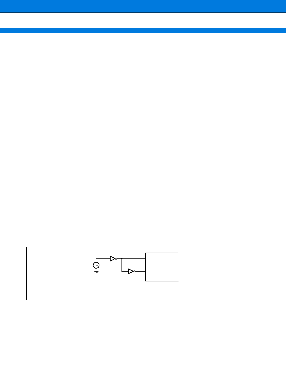
∑ Notes on Using External Clock
When external clock is selected, supply it to X0 pin generally, and simultaneously the opposite phase clock to
X0 must be supplied to X1 pin. However, in this case the stop mode(oscillator stop mode) must not be used.
(This is because the X1 pin stops at High level output in STOP mode.)
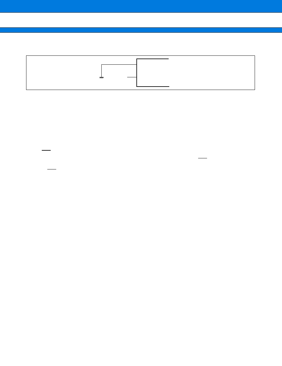
Using an external clock (normal)
∑ Clock control block
Take the oscillation stabilization wait time during Low level input to the INIT pin.
X0
X1
Note: STOP mode (oscillation stop mode) cannot be used.
MB91350A Series
18
∑ Notes on not using the sub clock
When no oscillator is connected to the X0A and X1A pins, pull down the X0A pin and open the X1A pin.
∑ Treatment of NC and OPEN pins
Pins marked as NC and OPEN must be left open-circuit.
∑ Mode pins (MD0 to MD2)
These pins should be connected directly to V
CC
or V
SS
.
To prevent the device erroneously switching to test mode due to noise, design the printed circuit board such that
the distance between the mode pins and V
CC
or V
SS
is as short as possible and the connection impedance is low.
∑ Operation at start-up
The INIT pin must be at Low level when the power supply is turned on.
Immediately after the power supply is turned on, hold the Low level input to the INIT pin for the settling time
required for the oscillator circuit to take the oscillation stabilization wait time for the oscillator circuit. (For INIT
via the INIT pin, the oscillation stabilization wait time setting is initialized to the minimum value.)
∑ About oscillation input at power on
When turning the power on, maintain clock input until the device is released from the oscillation stabilization
wait state.
∑ Caution on Operations during PLL Clock Mode
Even if the oscillator comes off or the clock input stops with the PLL clock selected for this microcontroller, the
microcontroller may continue to operate at the free-running frequency of the PLL's internal self-oscillating oscil-
lator circuit. Performance of this operation, however, cannot be guaranteed.
∑ External bus setting
This model guarantees an external bus frequency of 25 MHz.
Setting the base clock frequency to 50 MHz with DIVR1 (external bus base clock division setting register)
initialized sets the external bus frequency also to 50 MHz. Before changing the base clock frequency, set the
external bus frequency not exceeding 25 MHz.
∑ MCLK and SYSCLK
MCLK and SYSCLK has a difference that MCLK stops in SLEEP/STOP mode but SYSCLK stops only in STOP
mode. Use either depending on each application.
Upon initialization, MCLK becomes invalid (PORT) and SYSCLK becomes valid. To use MCLK, set the port
function register (PFR) to select the use of that clock.
∑ Pull-up control
Connecting a pull-up resistor to the pin serving as an external bus pin cannot a guarantee the "
ELECTRICAL
CHARACTERISTICS 4. AC Characteristics (4) Normal Bus Access Read/Write Operation, (5) Multiplex Bus
Access Read/Write operation and (7) Hold Timing".
Even the port for which a pull-up resistor has been set is invalid in stop mode with HIZ = 1 or in hardware standby
mode.
X0
X1
MB91350A
OPEN

MB91350A Series
19
∑ Sub clock select
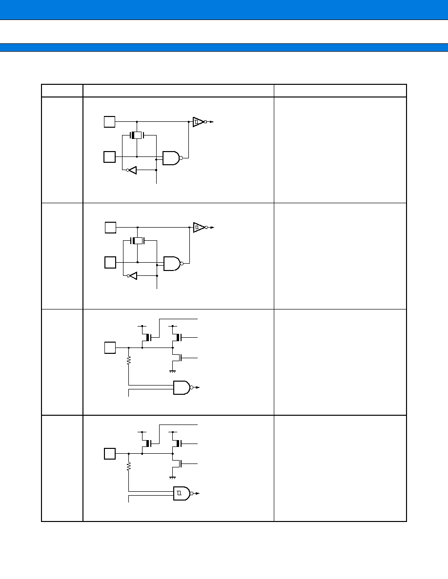
Immediately after switching from main clock mode to subclock mode for the clock source, insert at least one
NOP instruction.
∑ Bit Search Module
The BSD0, BSD1, and BDSC registers are accessed only in words.
∑ D-bus memory
Do not allocate the code area in memory on the D-bus because no instruction fetch takes place to the D-bus.
Executing an instruction fetch to the D-bus area causes wrong data to be interpreted as code, possibly letting
the device to run out of control.
∑ Low Power Consumption Mode
To enter the sleep or stop mode, be sure to read the standby control register (STCR) immediately after writing to it.
Precisely, use the following sequence.
Set the I flag, ILM, and ICR to, after returning from standby mode, branch to the interrupt handler having caused
the device to return.
∑ Switch shared port function
To switch between the use as a port and the use as a dedicated pin, use the port function register (PFR). Note,
however, that bus pins are switched depending on external bus settings.
∑ Pre-fetch
When accessing a prefetch-enabled little endian area, be sure to use word access (in 32-bit, word length) only.
Byte or halfword access results in wrong data read.
∑ I/O port access
Ports are accessed only in bytes.
∑ Built-in RAM
Immediately after a reset is canceled, the internal RAM allocation restricting function is still working, allowing
only 4 KB to be used for data and for program execution irrespective of the on-chip RAM capacity.
(ldi
#0x0b, r0)
(ldi
#_CLKR, r12)
stb
r0, @r12
// sub-clock mode
nop
// Must insert NOP instruction
(ldi
#value_of_standby, r0)
(ldi
#_STCR, r12)
stb
r0, @r12
// set STOP/SLEEP bit
ldub
@r12, r0
// Must read STCR
ldub
@r12, r0
// after reading, go into standby
mode
nop
// Must insert NOP *5
nop
nop
nop
nop

MB91350A Series
20
∑ Flash memory
In programming mode, Flash memory cannot be used as an interrupt vector table. A reset is possible.
∑ Notes on the PS register
As the PS register is processed by some instructions in advance, exception handling below may cause the
interrupt handling routine to break when the debugger is used or the display contents of flags in the PS register
to be updated.
As the microcontroller is designed to carry out reprocessing correctly upon returning from such an EIT event, it
performs operations before and after the EIT as specified in either case.
1. The following operations are performed when the instruction followed by a DIVOU/DIVOS instruction results in:
(a) acceptance of a user interrupt or NMI, (b) single-stepping, or (c) a break at a data event or emulator menu.
∑
The D0 and D1 flags are updated in advance.
∑
An EIT handling routine (user interrupt, NMI, or emulator) is executed.
∑
Upon returning from the EIT, the DIVOU/DIVOS instruction is executed and the D0 and D1 flags are
updated to the same values as in (1).
2. The following operations are performed when the ORCCR/STILM/MOVRi and PS instructions are executed.
∑
The PS register is updated in advance.
∑
An EIT handling routine (user interrupt, NMI, or emulator) is executed.
∑
Upon returning from the EIT, the above instructions are executed and the PS register is updated to the
same value as in (1).

MB91350A Series
21
[Note on debugger]
∑ Step execution of RETI command
If an interrupt occurs frequently during single-stepping, the corresponding interrupt handling routine is executed
repeatedly. This will prevent the main routine and low-interrupt-level programs from being executed. (Whenever
RETI is single-stepped when interrupts by the timebase timer have been enabled, for example, the timebase
timer routine causes a break at the beginning.)
Disable the corresponding interrupt when the corresponding interrupt handling routine no longer needs debug-
ging.
∑ Break function
If the address at which to cause a hardware break (including a event break) is set to the address currently
contained in the system stack pointer or in the area containing the stack pointer, the user program causes a
break after execution of one instruction.
To prevent this, do not set (word) access to the area containing the address in the system stack pointer as the
target of a hardware break (including an event break).
∑ Internal ROM area
Do not set an area of internal ROM as a DMAC transfer destination.
∑ Simultaneous occurrences of a software break (INTE instruction) and a user interrupt/NMI
When an INTE instruction and a user interrupt/NMI are accepted simultaneously, the emulator debugger reacts
as follows.
The emulator debugger stops while indicating a location in the user program, which is not a user-specified
breakpoint. (It stops with the beginning of the user interrupt/NMI handling routine indicated.)
The user program cannot be re-executed correctly.
To prevent this problem, follow the instructions below.
When a software break and a user interrupt/NMI occur simultaneously, the emulator debugger may react as
follows.
∑ The debugger stops pointing to a location other than the programmed breakpoints.
∑ The halted program is not re-executed correctly.
If this symptom occurs, use a hardware break in place of a hardware break. When using a monitor debugger,
do not set a break at the relevant location.
∑ A stack pointer placed in an area set for a DSU operand break can cause a malfunction. Do not apply a data
event break to access to the area containing the address of a system stack pointer.
MB91350A Series
22
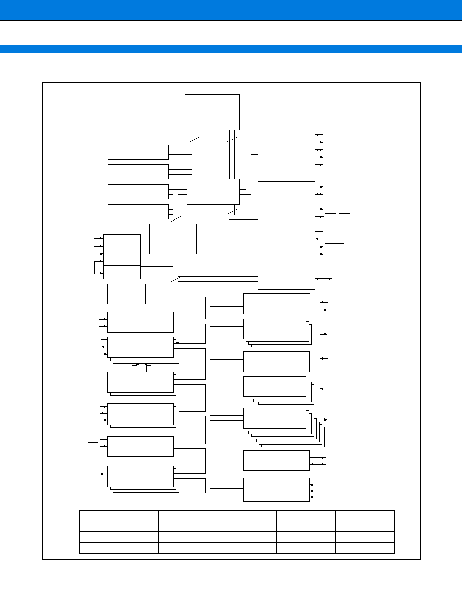
BLOCK DIAGRAM
DMAC 5 channels
PORT I/F
1 channel
I
2
C
FR CPU
Bus
Converter
32
32
32
32
32
16
Adapter
ROM/Flash
RAM (Executable)
16
5 channels
UART
5 channels
U-Timer
X0, X1
MD0 to MD2
INIT
INT0 to INT15
NMI
SI0 to SI4
SO0 to SO4
SCK0 to SCK4
SI5 to SI7
SO5 to SO7
SCK5 to SCK7
DA0 to DA2
DA
VC
, DA
VS
12 channels
A/D
AN0 to AN11
ATG
AVRH, AV
CC
AV
SS
/AVRL
DREQ0 to DREQ2
DACK0 to DACK2
DEOP0/DSTP0 to DEOP2/DSTP2
IOWR
IORD
A23 to A00
D31 to D16
RD
WR1, WR0
RDY
BRQ
BGRNT
SYSCLK
PORT
TRG0 to TRG5
PPG0 to PPG5
FRCK
IN0 to IN3
OC0 to OC7
AIN0, AIN1
BIN0, BIN1
ZIN0, ZIN1
SDA
SCL
TOT0 to TOT3
3 channels
SIO
X0A, X1A
Bit search
RAM (Stack)
Clock
control
Interrupt
DMAC (DMA
Controller)
16 channels
External interrupt
3 channels
D/A
8 channels
output compare
4 channels
input capture
16-bit free-run
timer
2 channels
8/16-bit up/down
counter
4 channels
reload timer
6 channels
PPG
External
memory
I/F
Clock timer
MB91F355A
MB91F356B
MB91355A
MB91354A
ROM/Flash
512 KB (Flash)
256 KB (Flash)
512 KB
384 KB
RAM (Stack)
16 KB
16 KB
16 KB
16 KB
RAM (Executable)
8 KB
8 KB
8 KB
8 KB

MB91350A Series
23
CPU AND CONTROL UNIT
Internal architecture
The FR family CPU is a high performance core based on a RISC architecture while incorporating advanced
instructions for embedded controller applications.
1.
Features
∑ RISC architecture employed. Basic instructions: Executed at 1 instruction per cycle
∑ General-purpose registers: 32-bit
◊
16 registers
∑ 4GB linear memory space
∑ Multiplier integrated.
32-bit x 32-bit multiplication: 5 cycles.
16-bit x 16-bit multiplication: 3 cycles
∑ Enhanced interrupt servicing.
Fast response speed (6 cycles).
Multiple interrupts supported.
Level masking (16 levels)
∑ Enhanced I/O manipulation instructions.
Memory-to-memory transfer instructions, Bit manipulation instructions
∑ High code efficiency. Basic instruction word length: 16-bit
∑ Low-power consumption. Sleep mode and stop mode
∑ Gear function
MB91350A Series
24
2.
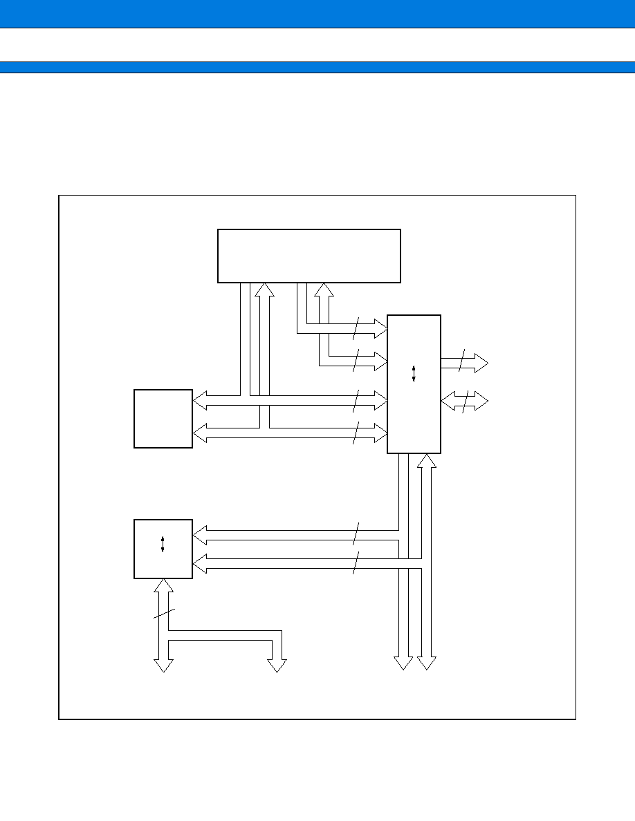
Internal architecture
The FR-family CPU has a Harvard architecture in which the instruction and data buses are separated.
The 32-bit/16-bit bus converter is connected to a 32-bit bus (F-bus), providing an interface between the CPU
and peripheral resources. The Harvard-Princeton bus converter is connected to both of the I-bus and D-bus,
providing an interface between the CPU and the bus controller.
FR CPU
Data
RAM
32-bit
16-bit
bus converter
Harvard
Princeton
bus
converter
D-bus
I-bus
D address
I address
External address
External data
D data
Address
Data
16
16
24
32
32
32
32
32
32
I data
R-bus
F-bus
Peripherals resource
Internal I/O
bus controller
MB91350A Series
25
3.
Programming model
∑ Basic programming model
R0
R1
R12
R13
R14
R15
PC
PS
ILM
SCR
CCR
TBR
RP
SSP
USP
MDH
MDL
AC
FP
SP
XXXX XXXX
H
XXXX XXXX
H
0 0 0 0 0 0 0 0
H
32-bit
Initial Value:
GENERAL
PURPOSE
REGISTERS
Program counter
program status
Table base register
Return pointer
System stack pointer
User stack pointer
Multiplication and division
result register
MB91350A Series
26
4.
Register
General purpose registers
Registers R0 to R15 are general-purpose registers. The registers are used as the accumulator and memory
access pointers for CPU operations.
Of these 16 registers, the registers listed below are intended for special applications, for which some instructions
are enhanced.
R13 : Virtual accumulator
R14 : frame pointer
R15 : Stack pointer
The initial values of R0 to R14 after a reset are indeterminate. R15 is initialized to 0000 0000
H
(SSP value).
∑ PS (Program Status)
This register holds the program status and is divided into the ILM, SCR, and CCR.
The undefined bits in the following illustration are all reserved bits. Reading these bits always returns "0". Writing
to them has no effect.
R0
R1
R12
R13
R14
R15
AC
FP
SP
XXXX XXXX
H
XXXX XXXX
H
0 0 0 0 0 0 0 0
H
32-bit
Initial Value:
Bit position
PS
31
20
16
ILM
SCR
CCR
10
7
8
0
MB91350A Series
27
∑ CCR (Condition Code Register )
∑ SCR (System Condition code Register )
Flag for step dividing
Stores intermediate data for stepwise multiplication operations.
Step trace trap flag
A flag specifying whether the step trace trap function is enabled or not.
Emulator use step trace trap function. The function cannot be used by the user program when using
the emulator.
∑ ILM
This register stores the interrupt level mask value. The value in the ILM register is used as the level mask.
Initialized to "15" (01111
B
) by a reset.
∑ PC (Program Counter)
The program counter contains the address of the instruction currently being executed.
The initial value after a reset is indeterminate.
S
: Stack flag. Cleared to "0" by a reset.
I
: Interrupt enable flag. Cleared to "0" by a reset.
N
: Negative flag. The initial value after a reset is indeterminate.
Z
: Zero flag. The initial value after a reset is indeterminate.
V
: Overflow flag. The initial value after a reset is indeterminate.
C
: Carry flag. The initial value after a reset is indeterminate.
Initial Value:
- - 00XXXX
B
CCR
7
6
5
4
3
2
1
0
S
I
N
Z
V
C
Initial Value:
XX0
B
SCR
10
9
8
D1
D0
T
Initial Value:
01111
B
ILM
20
19
18
17
16
ILM4 ILM3 ILM2 ILM1 ILM0
Initial Value:
XXXXXXXX
H
PC
31
0
PC

MB91350A Series
28
∑ TBR (Table Base Register)
The table base register contains the start address of the vector table used for servicing EIT events.
The initial value after a reset is 000FFC00
H
∑ RP (Return Pointer)
The return pointer contains the address to which to return from a subroutine.
When the CALL instruction is executed, the value in the PC is transferred to the RP.
When the RET instruction is executed, the value in the RP is transferred to the PC.
The initial value after a reset is indeterminate.
∑ SSP (System Stack Pointer)
The SSP is the system stack pointer and functions as R15 when the S flag is "0".
The SSP can be explicitly specified.
The SSP is also used as the stack pointer that specifies the stack for saving the PS and PC when an EIT event
occurs.
The initial value after a reset is 00000000
H
∑ USP (User Stack Pointer)
The USP is the user stack pointer and functions as R15 when the S flag is "1".
The SSP can be explicitly specified.
The initial value after a reset is indeterminate.
This pointer cannot be used by the RETI instruction.
Initial Value:
0 0 0 FFC0 0
H
TBR
31
0
TBR
Initial Value:
XXXXXXXX
H
RP
31
0
RP
Initial Value:
0 0 0 0 0 0 0 0
H
SSP
31
0
SSP
Initial Value:
XXXXXXXX
H
USP
31
0
USP

MB91350A Series
29
∑ Multiply & Divide registers
These registers hold the results of a multiplication or division. Each of them is 32-bit long.
The initial value after a reset is indeterminate.
Multiplication and division result register
31
0
MDH
MDL
MB91350A Series
30
MODE SETTINGS
The FR family uses mode pins (MD2 to MD0) and a mode register (MODR) to set the operation mode.
1.
Mode Pins
The MD2, MD1, and MD0 pins specify how the mode vector fetch is performed.
Values other than those listed in the table are prohibited.
2.
Mode Register (MODR)
The data written to the mode register at 000F FFF8
H
using mode vector fetch is called mode data.
After an operation mode has been set in the mode register (MODR), the device operates in the operation mode.
The mode register is set by any reset source. User programs cannot write data to the mode register.
Note : Conventionally the FR family has nothing at addresses (0000 07FF
H
) in the mode register.
<Register description>
[bit 7 to bit 3] Reserved bit
Be sure to set this bit to "00000". Operation is not guaranteed when any value other than "00000" is set.
[bit 2] ROMA (internal ROM enable bit)
The ROMA bit is used to set whether to enable the internal F-bus RAM and F-bus ROM areas.
Mode Pins
Mode name
Reset vector
access area
Remarks
MD2 MD1 MD0
0
0
0
Internal ROM mode vector
Internal
0
0
1
External ROM mode vector
External
The bus width is specified by the mode register.
ROMA
function
Remarks
0
External ROM mode
Internal F-bus RAM is valid; the area (80000
H
to 100000
H
) of internal ROM is used
as an external area.
1
Internal ROM mode Internal F-bus RAM and F-bus ROM become valid.
MODR
Initial Value
000F FFF8
H
XXXXXXXX
B
7
6
5
4
3
2
1
0
0
0
0
0
0
ROMA
WTH1
WTH0
Operation mode setting bits
MB91350A Series
31
[bit 1, bit 0] WTH1, WTH0 (Bus width setting bits)
Used to set the bus width to be used in external bus mode.
When the operation mode is the external bus mode, this value is set in bits BW1 and BW0 in AMD0 (CS0 area).
WTH1
WTH0
function
Remarks
0
0
8-bit bus width
External bus mode
0
1
16-bit bus width
1
0
Setting disabled
1
1
single chip mode
single chip mode
MB91350A Series
32
MEMORY SPACE
1.
Memory space
The FR family has 4 GB of logical address space (2
32
addresses) available to the CPU by linear access.
∑ Direct Addressing Areas
The following address space areas are used as I/O areas.
These areas are called direct addressing areas, in which the address of an operand can be specified directly
during an instruction.
The size of directly addressable areas depends on the length of the data being accessed as shown below.
byte data access
: 000
H
to 0FF
H
half word data access : 000
H
to 1FF
H
word data access
: 000
H
to 3FF
H
2.
Memory Map
∑
Memory map of MB91F355A/MB91355A
∑ Each mode is set depending on the mode vector fetch after INIT is negated.
∑ The MB91V350A uses the area of 512 KB of internal ROM as emulation RAM in the MB91355A memory map.
The internal RAM (Instruction) has been expanded from 8 KB to 16 KB.
∑ The available area of internal RAM is restricted immediately after a reset is canceled. When the setting of the
available area is updated, the instruction must be followed by at least 1 NOP instruction.
0008 0000
H
0000 0000
H
0000 0400
H
0001 0000
H
0003 E000
H
0004 0000
H
0004 4000
H
0005 0000
H
0010 0000
H
FFFF FFFF
H
I/O
I/O
I/O
I/O
I/O
I/O
Single chip mode
Internal ROM
external bus mode
Access
disallowed
Direct
addressing area
Refer to "3. I/O Map"
Built-in RAM 8 KB
(Executable)
Built-in RAM
512 KB
Access
disallowed
Access
disallowed
Built-in RAM 8 KB
(
Executable
)
Built-in RAM
512 KB
External area
Access
disallowed
Built-in RAM 8 KB
(Executable)
External area
Built-in RAM 16 KB
(Stack)
Access
disallowed
External ROM
external bus mode
External area
Access
disallowed
Access
disallowed
Built-in RAM 16 KB
(Stack)
Built-in RAM 16 KB
(Stack)
MB91350A Series
33
∑
Memory Map of MB91354A
∑ Each mode is set depending on the mode vector fetch after INIT is negated.
∑ The available area of internal RAM is restricted immediately after a reset is canceled. When the setting of the
available area is updated, the instruction must be followed by at least 1 NOP instruction.
0008 0000
H
0000 0000
H
0000 0400
H
0001 0000
H
0003 E000
H
0004 0000
H
0004 2000
H
0005 0000
H
0010 0000
H
FFFF FFFF
H
I/O
I/O
I/O
I/O
I/O
I/O
000A 0000
H
Single chip mode
Internal ROM
external bus mode
Access
disallowed
Direct
addressing area
Refer to "3. I/O Map"
Built-in RAM 8 KB
(Executable)
Built-in ROM
384 KB
Access
disallowed
Access
disallowed
Built-in RAM 8 KB
(Executable)
Built-in ROM
384 KB
External area
Access
disallowed
Built-in RAM 8 KB
(Executable)
External area
Built-in RAM 8 KB
(Stack)
Access
disallowed
External ROM
external bus mode
External area
Access
disallowed
Access
disallowed
Built-in RAM 8 KB
(Stack)
Built-in RAM 8 KB
(Stack)
Access
disallowed

MB91350A Series
34
∑
Memory Map of MB91356B
∑ Each mode is set depending on the mode vector fetch after INIT is negated.
∑ The available area of internal RAM is restricted immediately after a reset is canceled. When the setting of the
available area is updated, the instruction must be followed by at least 1 NOP instruction.
0008 0000
H
0000 0000
H
0000 0400
H
0001 0000
H
0003 E000
H
0004 0000
H
0004 4000
H
0005 0000
H
0010 0000
H
FFFF FFFF
H
I/O
I/O
I/O
I/O
I/O
I/O
000C 0000
H
Single chip mode
Internal ROM
external bus mode
Access
disallowed
Direct
addressing area
Refer to "3. I/O Map"
Built-in RAM 8 KB
(Executable)
Built-in ROM
256 KB
Access
disallowed
Access
disallowed
Built-in RAM 8 KB
(Executable)
Built-in ROM
256 KB
External area
Access
disallowed
Built-in RAM 8 KB
(Executable)
External area
Built-in RAM 16 KB
(Stack)
Access
disallowed
External ROM
external bus mode
External area
Access
disallowed
Access
disallowed
Built-in RAM 16 KB
(Stack)
Built-in RAM 16 KB
(Stack)
Access
disallowed
MB91350A Series
35
3.
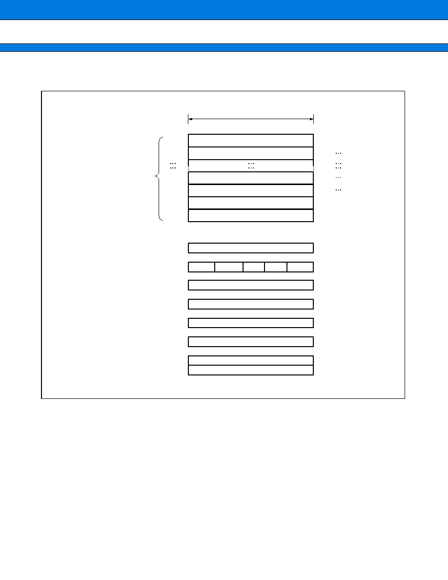
I/O Map
This shows the location of the various peripheral resource registers in the memory space.
(How to read the table)
Note : Initial values of register bits are represented as follows :
(Continued)
"1" : Initial value is "1".
"0" : Initial Value: "0".
"X" : Initial value is "X".
"
-
" : No physical register at this location
Address
Register
Block
diagram
+
0
+
1
+
2
+
3
000000
H
PDR2 [R/W] B
XXXXXXXX
PDR3 [R/W] B
XXXXXXXX
T-unit
Port Data
Register
000004
H
PDR4 [R/W] B
XXXXXXXX
PDR5 [R/W] B
XXXXXXXX
PDR6 [R/W] B
XXXXXXXX
000008
H
PDR8 [R/W] B
- - XXXXXX
PDR9 [R/W] B
- - - XXXXX
PDRA [R/W] B
- - - - XXXX
PDRB [R/W] B
XXXXXXXX
00000C
H
PDRC [R/W] B
- - - - - XXX
000010
H
PDRG[R/W] B
- - XXXXXX
PDRH [R/W] B
- - XXXXXX
PDRI [R/W] B
- - XXXXXX
PDRJ [R/W] B
XXXXXXXX
R-bus
Port Data
Register
000014
H
PDRK [R/W] B
XXXXXXXX
PDRL [R/W] B
- - - - - - XX
PDRM [R/W] B
- - XXXXXX
PDRN [R/W] B
- - XXXXXX
000018
H
PDRO [R/W] B
XXXXXXXX
PDRP [R/W] B
- - - - XXXX
00001C
H
000020
H
Reserved
000024
H
SMCS5 [R/W] B, H*
3
00000010 - - - - 00 - -
SES5 [R/W] B*
3
- - - - - - 00
SDR5 [R/W] B*
3
XXXXXXXX
SIO 5*
3
Address
Register
Block diagram
+
0
+
1
+
2
+
3
000000
H
PDR0 [R/W] B
XXXXXXXX
PDR1 [R/W] B
XXXXXXXX
PDR2 [R/W] B
XXXXXXXX
PDR3 [R/W] B
XXXXXXXX
T-unit
Port Data Register
Read/write attribute, Access unit
(B : Byte, H : Half Word, W : Word)
Initial value after a reset
Register name (First-column register at address 4n, second-column register at
address 4n + 2)
Location of left-most register (When using word access, the register in column
1 is in the MSB side of the data.)

MB91350A Series
36
(Continued)
Address
Register
Block
diagram
+
0
+
1
+
2
+
3
000028
H
SMCS6 [R/W] B, H
00000010 - - - - 00 - -
SES6 [R/W] B
- - - - - - 00
SDR6 [R/W] B
XXXXXXXX
SIO 6
00002C
H
SMCS7 [R/W] B, H
00000010 - - - - 00 - -
SES7 [R/W] B
- - - - - - 00
SDR7 [R/W] B
XXXXXXXX
SIO 7
000030
H
CDCR5 [R/W] B
0---1111
*
1
SIO Prescaler
5
000034
H
CDCR6 [R/W] B
0 - - - 1111
*
1
CDCR7 [R/W] B
0 - - - 1111
*
1
SIO Prescaler
6, 7
000038
H
SRCL5 [W] B
- - - - - - - -
SRCL6 [W] B
- - - - - - - -
SRCL7 [W] B
- - - - - - - -
SIO5 to SIO7
00003C
H
Reserved
000040
H
EIRR0 [R/W] B, H, W
00000000
ENIR0 [R/W] B, H, W
00000000
ELVR0 [R/W] B, H, W
00000000
Ext int
(INT0 to INT7)
000044
H
DICR [R/W] B, H, W
- - - - - - - 0
HRCL [R/W] B, H, W
0 - - 11111
DLYI/I-unit
000048
H
TMRLR [W] H, W
XXXXXXXX XXXXXXXX
TMR [R] H, W
XXXXXXXX XXXXXXXX
Reload Timer 0
00004C
H
TMCSR [R/W] B, H, W
- - - - 0000 00000000
000050
H
TMRLR [W] H, W
XXXXXXXX XXXXXXXX
TMR [R] H, W
XXXXXXXX XXXXXXXX
Reload Timer 1
000054
H
TMCSR [R/W] B, H, W
- - - - 0000 00000000
000058
H
TMRLR [W] H, W
XXXXXXXX XXXXXXXX
TMR [R] H, W
XXXXXXXX XXXXXXXX
Reload Timer 2
00005C
H
TMCSR [R/W] B, H, W
- - - - 0000 00000000
000060
H
SSR [R/W] B, H, W
00001000
SIDR/SODR [R/W]
B, H, W
XXXXXXXX
SCR [R/W] B, H, W
00000100
SMR [R/W] B, H, W
00 - - 0 - - -
UART0
000064
H
UTIM [R] H (UTIMR [W] H)
00000000 00000000
DRCL [W] B
- - - - - - - -
UTIMC [R/W] B
0 - - 00001
U-Timer/
UART 0
000068
H
SSR [R/W] B, H, W
00001000
SIDR/SODR [R/W]
B, H, W
XXXXXXXX
SCR [R/W] B, H, W
00000100
SMR [R/W] B, H, W
00 - - 0 - - -
UART1
00006C
H
UTIM [R] H (UTIMR [W] H)
00000000 00000000
DRCL [W] B
- - - - - - - -
UTIMC [R/W] B
0 - - 00001
U-Timer/
UART 1
000070
H
SSR [R/W] B, H, W
00001000
SIDR/SODR [R/W]
B, H, W
XXXXXXXX
SCR [R/W] B, H, W
00000100
SMR [R/W] B, H, W
00 - - 0 - - -
UART2
000074
H
UTIM [R] H (UTIMR [W] H)
00000000 00000000
DRCL [W] B
- - - - - - - -
UTIMC [R/W] B
0 - - 00001
U-Timer/
UART 2
MB91350A Series
37
(Continued)
Address
Register
Block
diagram
+
0
+
1
+
2
+
3
000078
H
ADCS2 [R/W]B, H, W
X000XX00
ADCS1 [R/W]B, H, W
000X0000
ADCT [R/W] H, W
XXXXXXXX_XXXXXXXX
A/D
converter:
Successive
approxima-
tion
00007C
H
ADTH0 [R] B, H, W
XXXXXXXX
ADTL0 [R] B, H, W
000000XX
ADTH1 [R] B, H, W
XXXXXXXX
ADTL1 [R] B, H, W
000000XX
000080
H
ADTH2 [R] B, H, W
XXXXXXXX
ADTL2 [R] B, H, W
000000XX
ADTH3 [R] B, H, W
XXXXXXXX
ADTL3 [R] B, H, W
000000XX
000084
H
DACR2 [R/W] B, H, W
- - - - - - - 0
DACR1 [R/W] B, H, W
- - - - - - - 0
DACR0 [R/W] B, H, W
- - - - - - - 0
D/A
Converter
000088
H
DADR2 [R/W] B, H, W
XXXXXXXX
DADR1 [R/W] B, H, W
XXXXXXXX
DADR0 [R/W] B, H, W
XXXXXXXX
00008C
H
Reserved
000090
H
*
1
Reserved
000094
H
IBCR [R/W] B, H, W
00000000
IBSR [R] B, H, W
00000000
ITBA [R/W] B, H, W
- - - - - - 00 00000000
I
2
C
interface
000098
H
ITMK [R/W] B, H, W
00 - - - - 11 11111111
ISMK [R/W] B, H, W
01111111
ISBA [R/W] B, H, W
- 0000000
00009C
H
IDAR [R/W] B, H, W
00000000
ICCR [R/W] B, H, W
0 - 011111
IDBL [R/W] B, H, W
- - - - - - - 0
0000A0
H
*
1
*
1
Reserved
0000A4
H
*
1
*
1
*
1
0000A8
H
TMRLR [W] H, W
XXXXXXXX XXXXXXXX
TMR [R] H, W
XXXXXXXX XXXXXXXX
Reload
Timer 3
0000AC
H
TMCSR [R/W] B, H, W
- - - - 0000 00000000
0000B0
H
RCR1 [W] B, H, W
00000000
RCR0 [W] B, H, W
00000000
UDCR1 [R] B, H, W
00000000
UDCR0 [R] B, H, W
00000000
8/16-bit
Up/Down
Counter
0, 1
0000B4
H
CCRH0 [R/W] B, H, W
00001000
CCRL0 [R/W] B, H, W
00001000
CSR0 [R/W] B, H, W
00000000
0000B8
H
CCRH1 [R/W] B, H, W
00001000
CCRL1 [R/W] B, H, W
00001000
CSR1 [R/W] B, H, W
00000000
0000BC
H
Reserved
0000C0
H
SSR [R/W] B, H, W
00001000
SIDR/SODR [R/W]
B, H, W
XXXXXXXX
SCR [R/W] B, H, W
00000100
SMR [R/W] B, H, W
00 - - 0 - - -
UART3
0000C4
H
UTIM [R] H (UTIMR [W] H)
00000000 00000000
UTIMC [R/W] B
0 - - 00001
U-Timer/
UART 3
0000C8
H
SSR [R/W] B, H, W
00001000
SIDR/SODR [R/W]
B, H, W
XXXXXXXX
SCR [R/W] B, H, W
00000100
SMR [R/W] B, H, W
00 - - 0 - - -
UART4
MB91350A Series
38
(Continued)
Address
Register
Block
diagram
+
0
+
1
+
2
+
3
0000CC
H
UTIM [R] H (UTIMR [W] H)
00000000 00000000
UTIMC [R/W] B
0 - - 00001
U-Timer/
UART 4
0000D0
H
EIRR1 [R/W] B, H, W
00000000
ENIR1 [R/W]B, H, W
00000000
ELVR1 [R/W] B, H, W
00000000
Ext int
(INT8-15)
0000D4
H
TCDT [R/W] H, W
00000000 00000000
TCCS [R/W] B, H, W
00000000
16-bit
Free run
Timer
0000D8
H
IPCP1 [R] H, W
XXXXXXXX XXXXXXXX
IPCP0 [R] H, W
XXXXXXXX XXXXXXXX
16-bit ICU
0000DC
H
IPCP3 [R] H, W
XXXXXXXX XXXXXXXX
IPCP2 [R] H, W
XXXXXXXX XXXXXXXX
0000E0
H
ICS23 [R/W] B, H, W
00000000
ICS01 [R/W] B, H, W
00000000
0000E4
H
OCCP1 [R/W] H, W
XXXXXXXX XXXXXXXX
OCCP0 [R/W] H, W
XXXXXXXX XXXXXXXX
16-bit
OCU
*3
0000E8
H
OCCP3 [R/W] H, W
XXXXXXXX XXXXXXXX
OCCP2 [R/W] H, W
XXXXXXXX XXXXXXXX
0000EC
H
OCCP5 [R/W] H, W
XXXXXXXX XXXXXXXX
OCCP4 [R/W] H, W
XXXXXXXX XXXXXXXX
0000F0
H
OCCP7 [R/W] H, W
XXXXXXXX XXXXXXXX
OCCP6 [R/W] H, W
XXXXXXXX XXXXXXXX
0000F4
H
OCS23 [R/W] B, H, W
1110110 00001100
OCS01 [R/W] B, H, W
1110110 00001100
0000F8
H
OCS67 [R/W] B, H, W
1110110 00001100
OCS45 [R/W] B, H, W
1110110 00001100
0000FC
H
Reserved
000100
H
to
000114
H
Reserved
000118
H
GCN10 [R/W] H
00110010_00010000
GCN20 [R/W] B
00000000
PPG
Control 0
00011C
H
Reserved
000120
H
PTMR0 [R] H, W
11111111_11111111
PCSR0 [W] H, W
XXXXXXXX_XXXXXXXX
PPG0
000124
H
PDUT0 [W] H, W
XXXXXXXX_XXXXXXXX
PCNH0 [R/W] B, H, W
00000000
PCNL0 [R/W] B, H, W
00000000
000128
H
PTMR1 [R] H, W
11111111_11111111
PCSR1 [W] H, W
XXXXXXXX_XXXXXXXX
PPG1
00012C
H
PDUT1 [W] H, W
XXXXXXXX_XXXXXXXX
PCNH1 [R/W] B, H, W
00000000
PCNL1 [R/W] B, H, W
00000000
MB91350A Series
39
(Continued)
Address
Register
Block
diagram
+
0
+
1
+
2
+
3
000130
H
PTMR2 [R] H, W
11111111_11111111
PCSR2 [W] H, W
XXXXXXXX_XXXXXXXX
PPG2
000134
H
PDUT2 [W] H, W
XXXXXXXX_XXXXXXXX
PCNH2 [R/W] B, H, W
00000000
PCNL2 [R/W] B, H, W
00000000
000138
H
PTMR3 [R] H, W
11111111_11111111
PCSR3 [W] H, W
XXXXXXXX_XXXXXXXX
PPG3
00013C
H
PDUT3 [W] H, W
XXXXXXXX_XXXXXXXX
PCNH3 [R/W] B, H, W
00000000
PCNL3[R/W] B, H, W
00000000
000140
H
PTMR4 [R] H, W
11111111_11111111
PCSR4 [W] H, W
XXXXXXXX_XXXXXXXX
PPG4
000144
H
PDUT4 [W] H, W
XXXXXXXX_XXXXXXXX
PCNH4 [R/W] B, H, W
00000000
PCNL4 [R/W] B, H, W
00000000
000148
H
PTMR5 [R] H, W
11111111_11111111
PCSR5 [W] H, W
XXXXXXXX_XXXXXXXX
PPG5
00014C
H
PDUT5 [W] H, W
XXXXXXXX_XXXXXXXX
PCNH5 [R/W] B, H, W
00000000
PCNL5 [R/W] B, H, W
00000000
000150
H
to
0001FC
H
Reserved
000200
H
DMACA0 [R/W] B, H, W*
2
00000000 0000XXXX XXXXXXXX XXXXXXXX
DMAC
000204
H
DMACB0 [R/W] B, H, W
00000000 00000000 XXXXXXXX XXXXXXXX
000208
H
DMACA1 [R/W] B, H, W*
2
00000000 0000XXXX XXXXXXXX XXXXXXXX
00020C
H
DMACB1 [R/W] B, H, W
00000000 00000000 XXXXXXXX XXXXXXXX
000210
H
DMACA2 [R/W] B, H, W*
2
00000000 0000XXXX XXXXXXXX XXXXXXXX
000214
H
DMACB2 [R/W] B, H, W
00000000 00000000 XXXXXXXX XXXXXXXX
000218
H
DMACA3 [R/W] B, H, W*
2
00000000 0000XXXX XXXXXXXX XXXXXXXX
00021C
H
DMACB3 [R/W] B, H, W
00000000 00000000 XXXXXXXX XXXXXXXX
000220
H
DMACA4 [R/W] B, H, W*
2
00000000 0000XXXX XXXXXXXX XXXXXXXX
000224
H
DMACB4 [R/W] B, H, W
00000000 00000000 XXXXXXXX XXXXXXXX
000228
H
MB91350A Series
40
(Continued)
Address
Register
Block
diagram
+
0
+
1
+
2
+
3
00022C
H
to
00023C
H
Reserved
000240
H
DMACR [R/W] B
0XX00000 XXXXXXXX XXXXXXXX XXXXXXXX
DMAC
000244
H
to
00027C
H
Reserved
000280
H
FRLR [R/W] B, H, W
- - - - - - 01*
3
F-bus RAM
capacity limit
000284
H
to
00038C
H
Reserved
000390
H
DRLR [R/W] B, H, W
- - - - - - 01*
3
D-bus RAM
capacity limit
000394
H
to
0003EC
H
Reserved
0003F0
H
BSD0 [W]
XXXXXXXX XXXXXXXX XXXXXXXX XXXXXXXX
Bit Search
Module
0003F4
H
BSD1 [R/W]
XXXXXXXX XXXXXXXX XXXXXXXX XXXXXXXX
0003F8
H
BSDC [W]
XXXXXXXX XXXXXXXX XXXXXXXX XXXXXXXX
0003FC
H
BSRR [R]
XXXXXXXX XXXXXXXX XXXXXXXX XXXXXXXX
000400
H
DDRG[R/W] B
- - 000000
DDRH [R/W] B
- - 000000
DDRI [R/W] B
- - 000000
DDRJ [R/W] B
00000000
R-bus
Data
Direction
Register
000404
H
DDRK [R/W] B
00000000
DDRL [R/W] B
- - - - - - 00
DDRM [R/W] B
- - 000000
DDRN [R/W] B
- - 000000
000408
H
DDRO [R/W] B
00000000
DDRP [R/W] B
- - - - 0000
00040C
H
000410
H
PFRG [R/W] B
- - 00 - 00 -
PFRH [R/W] B
- - 00 - 00 -
PFRI [R/W] B
- - 00 - 00 -
R-bus
Port Function
Register
000414
H
________
PFRL [R/W] B
- - - - - - 00
PFRM [R/W] B
- - 00 - 00 -
PFRN [R/W] B
- - 000000
000418
H
PFRO [R/W] B
00000000
PFRP [R/W] B
- - - - 0000
00041C
H
Reserved
MB91350A Series
41
(Continued)
Address
Register
Block
diagram
+
0
+
1
+
2
+
3
000420
H
PCRG [R/W] B
- - 000000
PCRH [R/W] B
- - 000000
PCRI [R/W] B
- - 000000
R-bus
Pull-up
Control
Register
000424
H
PCRM [R/W] B
- - 000000
PCRN [R/W] B
- - 000000
000428
H
PCRO [R/W] B
00000000
PCRP [R/W] B
- - - - 0000
00042C
H
to
00043C
H
Reserved
000440
H
ICR00 [R/W] B, H, W
- - - 11111
ICR01 [R/W] B, H, W
- - - 11111
ICR02 [R/W] B, H, W
- - - 11111
ICR03 [R/W] B, H, W
- - - 11111
Interrupt
Control unit
000444
H
ICR04 [R/W] B, H, W
- - - 11111
ICR05 [R/W] B, H, W
- - - 11111
ICR06 [R/W] B, H, W
- - - 11111
ICR07 [R/W] B, H, W
- - - 11111
000448
H
ICR08 [R/W] B, H, W
- - - 11111
ICR09 [R/W] B, H, W
- - - 11111
ICR10 [R/W] B, H, W
- - - 11111
ICR11 [R/W] B, H, W
- - - 11111
00044C
H
ICR12 [R/W] B, H, W
- - - 11111
ICR13 [R/W] B, H, W
- - - 11111
ICR14 [R/W] B, H, W
- - - 11111
ICR15 [R/W] B, H, W
- - - 11111
000450
H
ICR16 [R/W] B, H, W
- - - 11111
ICR17 [R/W] B, H, W
- - - 11111
ICR18 [R/W] B, H, W
- - - 11111
ICR19 [R/W] B, H, W
- - - 11111
000454
H
ICR20 [R/W] B, H, W
- - - 11111
ICR21 [R/W] B, H, W
- - - 11111
ICR22 [R/W] B, H, W
- - - 11111
ICR23 [R/W] B, H, W
- - - 11111
000458
H
ICR24 [R/W] B, H, W
- - - 11111
ICR25 [R/W] B, H, W
- - - 11111
ICR26 [R/W] B, H, W
- - - 11111
ICR27 [R/W] B, H, W
- - - 11111
00045C
H
ICR28 [R/W] B, H, W
- - - 11111
ICR29 [R/W] B, H, W
- - - 11111
ICR30 [R/W] B, H, W
- - - 11111
ICR31 [R/W] B, H, W
- - - 11111
000460
H
ICR32 [R/W] B, H, W
- - - 11111
ICR33 [R/W] B, H, W
- - - 11111
ICR34 [R/W] B, H, W
- - - 11111
ICR35 [R/W] B, H, W
- - - 11111
000464
H
ICR36 [R/W] B, H, W
- - - 11111
ICR37 [R/W] B, H, W
- - - 11111
ICR38 [R/W] B, H, W
- - - 11111
ICR39 [R/W] B, H, W
- - - 11111
000468
H
ICR40 [R/W] B, H, W
- - - 11111
ICR41 [R/W] B, H, W
- - - 11111
ICR42 [R/W] B, H, W
- - - 11111
ICR43 [R/W] B, H, W
- - - 11111
00046C
H
ICR44 [R/W] B, H, W
- - - 11111
ICR45 [R/W] B, H, W
- - - 11111
ICR46 [R/W] B, H, W
- - - 11111
ICR47 [R/W] B, H, W
- - - 11111
000470
H
to
00047C
H
000480
H
RSRR [R/W] B, H, W
10000000
STCR [R/W] B, H, W
00110011
TBCR [R/W] B, H, W
00XXXX00
CTBR [W] B, H, W
XXXXXXXX
Clock
Control unit
000484
H
CLKR [R/W] B, H, W
00000000
WPR [W] B, H, W
XXXXXXXX
DIVR0 [R/W] B, H, W
00000011
DIVR1 [R/W] B, H, W
00000000
000488
H
OSCCR [R/W] B
XXXXXXX0
MB91350A Series
42
(Continued)
Address
Register
Block
diagram
+
0
+
1
+
2
+
3
00048C
H
WPCR [R/W] B
00 - - - 000
Clock timer
000490
H
OSCR [R/W] B
000 - - XX0
Main oscillation
stabilization
timer
000494
H
RSTOP0 [W] B
00000000
RSTOP1 [W] B
00000000
RSTOP2 [W] B
00000000
RSTOP3 [W] B
- - - - - 000
Peripheral stop
control
000498
H
Reserved
00049C
H
to
0005FC
H
Reserved
000600
H
DDR2 [R/W] B
00000000
DDR3 [R/W] B
00000000
T-unit
Data Direction
Register
000604
H
DDR4 [R/W] B
00000000
DDR5 [R/W] B
00000000
DDR6 [R/W] B
00000000
000608
H
DDR8 [R/W] B
- - 000000
DDR9 [R/W] B
- - - 00000
DDRA [R/W] B
- - - - 0000
DDRB [R/W] B
00000000
00060C
H
DDRC [R/W] B
- - - - - 000
000610
H
T-unit
Port Function
Register
000614
H
PFR6 [R/W] B
11111111
000618
H
PFR8 [R/W] B
- - 1 - - 0 - -
PFR9 [R/W] B
- - - 010 - 1
PFRA [R/W] B
- - - - 1111
PFRB1 [R/W] B
00000000
00061C
H
PFRB2 [R/W] B
00 - - - - 00
PFRC [R/W] B
- - - 00000
000620
H
PCR2 [R/W] B
00000000
PCR3 [R/W] B
00000000
T-unit
Pull-up Control
Register
000624
H
PCR4 [R/W] B
00000000
PCR5 [R/W] B
00000000
PCR6 [R/W] B
00000000
000628
H
PCR8 [R/W] B
--000000
PCR9 [R/W] B
00000000
PCRA [R/W] B
00000000
PCRB [R/W] B
00000000
00062C
H
PCRC [R/W] B
-----000
000630
H
to
00063C
H
Reserved
000640
H
ASR0 [R/W] H, W
00000000 00000000
ACR0 [R/W] B, H, W
1111XX00 00000000
T-unit
000644
H
ASR1 [R/W] H, W
00000000 00000000
ACR1 [R/W] B, H, W
XXXXXXXX XXXXXXXX
000648
H
ASR2 [R/W] H, W
00000000 00000000
ACR2 [R/W] B, H, W
XXXXXXXX XXXXXXXX
MB91350A Series
43
(Continued)
Address
Register
Block
diagram
+
0
+
1
+
2
+
3
00064C
H
ASR3 [R/W] H, W
00000000 00000000
ACR3 [R/W] B, H, W
XXXXXXXX XXXXXXXX
T-unit
000650
H
ASR4 [R/W] H, W
00000000 00000000
ACR4 [R/W] B, H, W
XXXXXXXX XXXXXXXX
000654
H
ASR5 [R/W] H, W
00000000 00000000
ACR5 [R/W] B, H, W
XXXXXXXX XXXXXXXX
000658
H
ASR6 [R/W] H, W
00000000 00000000
ACR6 [R/W] B, H, W
XXXXXXXX XXXXXXXX
00065C
H
ASR7 [R/W] H, W
00000000 00000000
ACR7 [R/W] B, H, W
XXXXXXXX XXXXXXXX
000660
H
AWR0 [R/W] B, H, W
01111111 11111111
AWR1 [R/W] B, H, W
XXXXXXXX XXXXXXXX
000664
H
AWR2 [R/W] B, H, W
XXXXXXXX XXXXXXXX
AWR3 [R/W] B, H, W
XXXXXXXX XXXXXXXX
000668
H
AWR4 [R/W] B, H, W
XXXXXXXX XXXXXXXX
AWR5 [R/W] B, H, W
XXXXXXXX XXXXXXXX
00066C
H
AWR6 [R/W] B, H, W
XXXXXXXX XXXXXXXX
AWR7 [R/W] B, H, W
XXXXXXXX XXXXXXXX
000670
H
000674
H
000678
H
IOWR0 [R/W] B, H, W
XXXXXXXX
IOWR1 [R/W] B, H, W
XXXXXXXX
IOWR2 [R/W] B, H, W
XXXXXXXX
00067C
H
000680
H
CSER [R/W] B, H, W
00000001
TCR [W] B, H, W
0000XXXX
000684
H
to
000AFC
H
Reserved
000B00
H
ESTS0 [R/W]
X0000000
ESTS1 [R/W]
XXXXXXXX
ESTS2 [R]
1XXXXXXX
DSU
(Evalua-
tion chip
only)
000B04
H
ECTL0 [R/W]
0X000000
ECTL1 [R/W]
00000000
ECTL2 [W]
000X0000
ECTL3 [R/W]
00X00X11
000B08
H
ECNT0 [W]
XXXXXXXX
ECNT1 [W]
XXXXXXXX
EUSA [W]
XXX00000
EDTC [W]
0000XXXX
MB91350A Series
44
(Continued)
Address
Register
Block
diagram
+
0
+
1
+
2
+
3
000B0C
H
EWPT [R]
00000000 00000000
DSU
(Evaluation
chip only)
000B10
H
EDTR0 [W]
XXXXXXXX XXXXXXXX
EDTR1 [W]
XXXXXXXX XXXXXXXX
000B14
H
to
000B1C
H
000B20
H
EIA0 [W]
XXXXXXXX XXXXXXXX XXXXXXXX XXXXXXXX
000B24
H
EIA1 [W]
XXXXXXXX XXXXXXXX XXXXXXXX XXXXXXXX
000B28
H
EIA2 [W]
XXXXXXXX XXXXXXXX XXXXXXXX XXXXXXXX
000B2C
H
EIA3 [W]
XXXXXXXX XXXXXXXX XXXXXXXX XXXXXXXX
000B30
H
EIA4 [W]
XXXXXXXX XXXXXXXX XXXXXXXX XXXXXXXX
000B34
H
EIA5 [W]
XXXXXXXX XXXXXXXX XXXXXXXX XXXXXXXX
000B38
H
EIA6 [W]
XXXXXXXX XXXXXXXX XXXXXXXX XXXXXXXX
000B3C
H
EIA7 [W]
XXXXXXXX XXXXXXXX XXXXXXXX XXXXXXXX
000B40
H
EDTA [R/W]
XXXXXXXX XXXXXXXX XXXXXXXX XXXXXXXX
000B44
H
EDTM [R/W]
XXXXXXXX XXXXXXXX XXXXXXXX XXXXXXXX
000B48
H
EOA0 [W]
XXXXXXXX XXXXXXXX XXXXXXXX XXXXXXXX
000B4C
H
EOA1 [W]
XXXXXXXX XXXXXXXX XXXXXXXX XXXXXXXX
000B50
H
EPCR [R/W]
XXXXXXXX XXXXXXXX XXXXXXXX XXXXXXXX
000B54
H
EPSR [R/W]
XXXXXXXX XXXXXXXX XXXXXXXX XXXXXXXX
000B58
H
EIAM0 [W]
XXXXXXXX XXXXXXXX XXXXXXXX XXXXXXXX
000B5C
H
EIAM1 [W]
XXXXXXXX XXXXXXXX XXXXXXXX XXXXXXXX
000B60
H
EOAM0/EODM0 [W]
XXXXXXXX XXXXXXXX XXXXXXXX XXXXXXXX
MB91350A Series
45
(Continued)
Address
Register
Block
diagram
+
0
+
1
+
2
+
3
000B64
H
EOAM1/EODM1 [W]
XXXXXXXX XXXXXXXX XXXXXXXX XXXXXXXX
DSU
(Evaluation
chip only)
000B68
H
EOD0 [W]
XXXXXXXX XXXXXXXX XXXXXXXX XXXXXXXX
000B6C
H
EOD1 [W]
XXXXXXXX XXXXXXXX XXXXXXXX XXXXXXXX
000B70
H
to
000BFC
H
Reserved
000C00
H
Register access disallowed
Interrupt
Control unit
000C04
H
to
000C14
H
Register access disallowed
R-bus test
000C18
H
to
000FFC
H
Reserved
001000
H
DMASA0 [R/W] W
XXXXXXXX_XXXXXXXX_XXXXXXXX_XXXXXXXX
DMAC
001004
H
DMADA0 [R/W] W
XXXXXXXX_XXXXXXXX_XXXXXXXX_XXXXXXXX
001008
H
DMASA1 [R/W] W
XXXXXXXX_XXXXXXXX_XXXXXXXX_XXXXXXXX
00100C
H
DMADA1 [R/W] W
XXXXXXXX_XXXXXXXX_XXXXXXXX_XXXXXXXX
001010
H
DMASA2 [R/W] W
XXXXXXXX_XXXXXXXX_XXXXXXXX_XXXXXXXX
001014
H
DMADA2 [R/W] W
XXXXXXXX_XXXXXXXX_XXXXXXXX_XXXXXXXX
001018
H
DMASA3 [R/W] W
XXXXXXXX_XXXXXXXX_XXXXXXXX_XXXXXXXX
00101C
H
DMADA3 [R/W] W
XXXXXXXX_XXXXXXXX_XXXXXXXX_XXXXXXXX
001020
H
DMASA4 [R/W] W
XXXXXXXX_XXXXXXXX_XXXXXXXX_XXXXXXXX
001024
H
DMADA4 [R/W] W
XXXXXXXX_XXXXXXXX_XXXXXXXX_XXXXXXXX
001028
H
to
001FFC
H
Reserved
MB91350A Series
46
(Continued)
*1 : Test register access barred
*2 : The lower 16-bit (DTC(15: 0)) of DMACA0 to DMACA4 cannot be accessed in byte.
*3 : The available area of internal RAM is restricted by the function described in 6-209 immediately after a reset is
canceled. When the setting of the available area is updated, the instruction must be followed by at least 1 NOP
instruction.
Address
Register
Block
diagram
+
0
+
1
+
2
+
3
007000
H
FLCR [R/W]
0110X000
Flash
memory
007004
H
FLWC [R/W]
00010011
007008
H
00700C
H
007010
H
007014
H
to
0070FF
H
Reserved
MB91350A Series
47
VECTOR TABLE
(Continued)
Interrupt source
Interrupt
number
Interrupt
level
Offset
TBR default
address
RN
10
16
Reset
0
00
3FC
H
000FFFFC
H
Mode vector
1
01
3F8
H
000FFFF8
H
System reserved
2
02
3F4
H
000FFFF4
H
System reserved
3
03
3F0
H
000FFFF0
H
System reserved
4
04
3EC
H
000FFFEC
H
System reserved
5
05
3E8
H
000FFFE8
H
System reserved
6
06
3E4
H
000FFFE4
H
Coprocessor absent trap
7
07
3E0
H
000FFFE0
H
Coprocessor error trap
8
08
3DC
H
000FFFDC
H
INTE instruction
9
09
3D8
H
000FFFD8
H
Instruction break exception
10
0A
3D4
H
000FFFD4
H
Operand break trap
11
0B
3D0
H
000FFFD0
H
Step trace trap
12
0C
3CC
H
000FFFCC
H
NMI request (tool)
13
0D
3C8
H
000FFFC8
H
Undefined instruction exception
14
0E
3C4
H
000FFFC4
H
NMI request
15
0F
15 (F
H
)
fixed15
3C0
H
000FFFC0
H
External interrupt 0
16
10
ICR00
3BC
H
000FFFBC
H
6
External interrupt 1
17
11
ICR01
3B8
H
000FFFB8
H
7
External interrupt 2
18
12
ICR02
3B4
H
000FFFB4
H
11
External interrupt 3
19
13
ICR03
3B0
H
000FFFB0
H
External interrupt 4
20
14
ICR04
3AC
H
000FFFAC
H
External interrupt 5
21
15
ICR05
3A8
H
000FFFA8
H
External interrupt 6
22
16
ICR06
3A4
H
000FFFA4
H
External interrupt 7
23
17
ICR07
3A0
H
000FFFA0
H
Reload timer 0
24
18
ICR08
39C
H
000FFF9C
H
8
Reload timer 1
25
19
ICR09
398
H
000FFF98
H
9
Reload timer 2
26
1A
ICR10
394
H
000FFF94
H
10
UART(Reception completed)
27
1B
ICR11
390
H
000FFF90
H
0
UART(Reception completed)
28
1C
ICR12
38C
H
000FFF8C
H
1
UART(Reception completed)
29
1D
ICR13
388
H
000FFF88
H
2
UART0 (RX completed)
30
1E
ICR14
384
H
000FFF84
H
3
UART1 (RX completed)
31
1F
ICR15
380
H
000FFF80
H
4
UART2 (RX completed)
32
20
ICR16
37C
H
000FFF7C
H
5
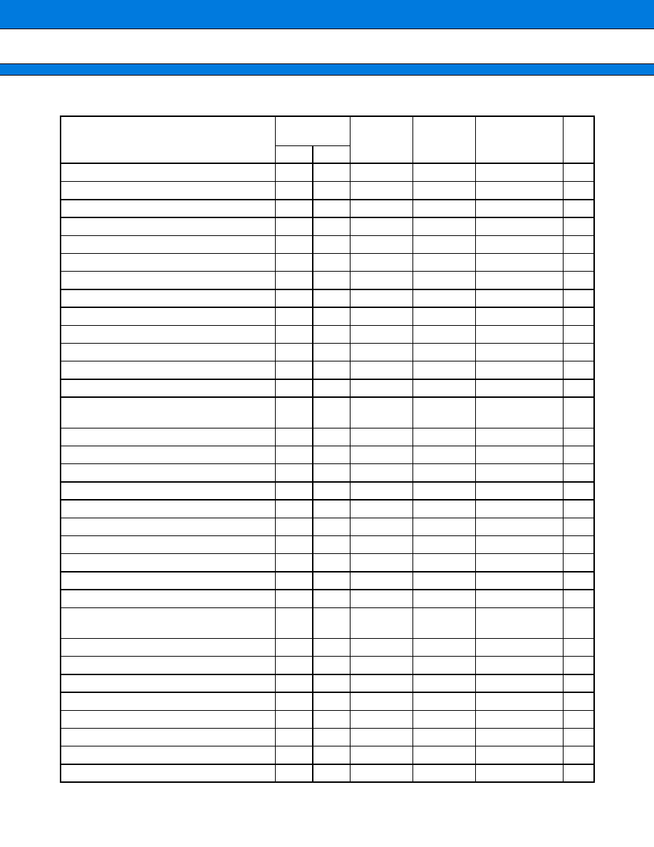
MB91350A Series
48
(Continued)
Interrupt source
Interrupt
number
Interrupt
level
Offset
TBR default
address
RN
10
16
DMAC0 (end, error)
33
21
ICR17
378
H
000FFF78
H
DMAC1 (end, error)
34
22
ICR18
374
H
000FFF74
H
DMAC2 (end, error)
35
23
ICR19
370
H
000FFF70
H
DMAC3 (end, error)
36
24
ICR20
36C
H
000FFF6C
H
DMAC4 (end, error)
37
25
ICR21
368
H
000FFF68
H
A/D
38
26
ICR22
364
H
000FFF64
H
15
I
2
C
39
27
ICR23
360
H
000FFF60
H
UART4 (Reception completed)
40
28
ICR24
35C
H
000FFF5C
H
SIO 5
41
29
ICR25
358
H
000FFF58
H
12
SIO 6
42
2A
ICR26
354
H
000FFF54
H
13
SIO 7
43
2B
ICR27
350
H
000FFF50
H
14
UART3 (Reception completed)
44
2C
ICR28
34C
H
000FFF4C
H
UART3 (RX completed)
45
2D
ICR29
348
H
000FFF48
H
Reload timer 3/main oscillation stabilization
wait timer
46
2E
ICR30
344
H
000FFF44
H
Timebase timer overflow
47
2F
ICR31
340
H
000FFF40
H
External interrupt: FPINT(8-15)
48
30
ICR32
33C
H
000FFF3C
H
Clock counter
49
31
ICR33
338
H
000FFF38
H
U/D Counter0
50
32
ICR34
334
H
000FFF34
H
U/D Counter1
51
33
ICR35
330
H
000FFF30
H
PPG 0/1
52
34
ICR36
32C
H
000FFF2C
H
PPG 2/3
53
35
ICR37
328
H
000FFF28
H
PPG 4/5
54
36
ICR38
324
H
000FFF24
H
16-bit free-run timer
55
37
ICR39
320
H
000FFF20
H
ICU2/3 (capture)
56
38
ICR40
31C
H
000FFF1C
H
ICU1 (capture)/UART4 (transmission
complete)
57
39
ICR41
318
H
000FFF18
H
ICU0 (capture)
58
3A
ICR42
314
H
000FFF14
H
OCU0/1 (match)
59
3B
ICR43
310
H
000FFF10
H
OCU2/3 (match)
60
3C
ICR44
30C
H
000FFF0C
H
OCU4/5 (match)
61
3D
ICR45
308
H
000FFF08
H
OCU6/7 (match)
62
3E
ICR46
304
H
000FFF04
H
Interrupt delay source bit
63
3F
ICR47
300
H
000FFF00
H
System reserved (Used by REALOS)
64
40
2FC
H
000FFEFC
H
System reserved (Used by REALOS)
65
41
2F8
H
000FFEF8
H
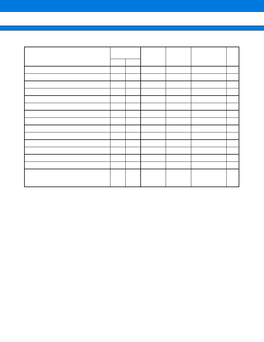
MB91350A Series
49
(Continued)
Interrupt source
Interrupt
number
Interrupt
level
Offset
TBR default
address
RN
10
16
System reserved
66
42
2F4
H
000FFEF4
H
System reserved
67
43
2F0
H
000FFEF0
H
System reserved
68
44
2EC
H
000FFEEC
H
System reserved
69
45
2E8
H
000FFEE8
H
System reserved
70
46
2E4
H
000FFEE4
H
System reserved
71
47
2E0
H
000FFEE0
H
System reserved
72
48
2DC
H
000FFEDC
H
System reserved
73
49
2D8
H
000FFED8
H
System reserved
74
4A
2D4
H
000FFED4
H
System reserved
75
4B
2D0
H
000FFED0
H
System reserved
76
4C
2CC
H
000FFECC
H
System reserved
77
4D
2C8
H
000FFEC8
H
System reserved
78
4E
2C4
H
000FFEC4
H
System reserved
79
4F
2C0
H
000FFEC0
H
Used by INT instruction
80
to
255
50
to
FF
2BC
H
to
000
H
000FFEBC
H
to
000FFC00
H
MB91350A Series
50
PERIPHERAL RESOURCES
1.
Interrupt controller
(1)Description
The interrupt controller manages interrupt reception and arbitration.
∑ Hardware configuration
This module consists of the following components:
∑ ICR register
∑ Interrupt priority determination circuit
∑ Interrupt level and interrupt number (vector) generator
∑ HOLD request cancellation request generator
∑ Main function
This module has the following major functions:
∑ Detect NMI and interrupt requests
∑ Prioritize interrupts (according to level and number)
∑ Notify interrupt level of selected interrupt request (to CPU)
∑ Notify interrupt number of selected interrupt request (to CPU)
∑ Request (to the CPU) to return from stop mode in response to an NMI or interrupt request with interrupt level
other than "11111"
∑ Hold request cancellation request issued to the bus master
(2)Register list
(Continued)
ICR register
7
6
5
4
3
2
1
0
ICR00
ICR4
ICR3
ICR2
ICR1
ICR0
ICR01
ICR4
ICR3
ICR2
ICR1
ICR0
ICR02
ICR4
ICR3
ICR2
ICR1
ICR0
ICR03
ICR4
ICR3
ICR2
ICR1
ICR0
ICR04
ICR4
ICR3
ICR2
ICR1
ICR0
ICR05
ICR4
ICR3
ICR2
ICR1
ICR0
ICR06
ICR4
ICR3
ICR2
ICR1
ICR0
ICR07
ICR4
ICR3
ICR2
ICR1
ICR0
ICR08
ICR4
ICR3
ICR2
ICR1
ICR0
ICR09
ICR4
ICR3
ICR2
ICR1
ICR0
ICR10
ICR4
ICR3
ICR2
ICR1
ICR0
ICR11
ICR4
ICR3
ICR2
ICR1
ICR0
ICR12
ICR4
ICR3
ICR2
ICR1
ICR0
ICR13
ICR4
ICR3
ICR2
ICR1
ICR0
ICR14
ICR4
ICR3
ICR2
ICR1
ICR0
ICR15
ICR4
ICR3
ICR2
ICR1
ICR0
MB91350A Series
51
(Continued)
Hold request cancel request resister (HRCL)
7
6
5
4
3
2
1
0
ICR16
ICR4
ICR3
ICR2
ICR1
ICR0
ICR17
ICR4
ICR3
ICR2
ICR1
ICR0
ICR18
ICR4
ICR3
ICR2
ICR1
ICR0
ICR19
ICR4
ICR3
ICR2
ICR1
ICR0
ICR20
ICR4
ICR3
ICR2
ICR1
ICR0
ICR21
ICR4
ICR3
ICR2
ICR1
ICR0
ICR22
ICR4
ICR3
ICR2
ICR1
ICR0
ICR23
ICR4
ICR3
ICR2
ICR1
ICR0
ICR24
ICR4
ICR3
ICR2
ICR1
ICR0
ICR25
ICR4
ICR3
ICR2
ICR1
ICR0
ICR26
ICR4
ICR3
ICR2
ICR1
ICR0
ICR27
ICR4
ICR3
ICR2
ICR1
ICR0
ICR28
ICR4
ICR3
ICR2
ICR1
ICR0
ICR29
ICR4
ICR3
ICR2
ICR1
ICR0
ICR30
ICR4
ICR3
ICR2
ICR1
ICR0
ICR31
ICR4
ICR3
ICR2
ICR1
ICR0
ICR32
ICR4
ICR3
ICR2
ICR1
ICR0
ICR33
ICR4
ICR3
ICR2
ICR1
ICR0
ICR34
ICR4
ICR3
ICR2
ICR1
ICR0
ICR35
ICR4
ICR3
ICR2
ICR1
ICR0
ICR36
ICR4
ICR3
ICR2
ICR1
ICR0
ICR37
ICR4
ICR3
ICR2
ICR1
ICR0
ICR38
ICR4
ICR3
ICR2
ICR1
ICR0
ICR39
ICR4
ICR3
ICR2
ICR1
ICR0
ICR40
ICR4
ICR3
ICR2
ICR1
ICR0
ICR41
ICR4
ICR3
ICR2
ICR1
ICR0
ICR42
ICR4
ICR3
ICR2
ICR1
ICR0
ICR43
ICR4
ICR3
ICR2
ICR1
ICR0
ICR44
ICR4
ICR3
ICR2
ICR1
ICR0
ICR45
ICR4
ICR3
ICR2
ICR1
ICR0
ICR46
ICR4
ICR3
ICR2
ICR1
ICR0
ICR47
ICR4
ICR3
ICR2
ICR1
ICR0
7
6
5
4
3
2
1
0
HRCL
MHALT1
LVL4
LVL3
LVL2
LVL1
LVL0
MB91350A Series
52
(3)Block diagram
RI00
5
6
LEVEL4 to LEVEL0
MHALTI
VCT5 to
VCT0
R-bus
UNMI
WAKEUP
ICR00
NMI
NMI
("1" when LEVEL
11111)
Determine order of priority
LEVEL determination
VECTOR
determination
LEVEL,
VECTOR
Genera-
tion
HLDREQ
Cancel
NMI
request
MB91350A Series
53
2.
External interrupt/NMI control
(1)Description
The external interrupt control unit is the block that controls external interrupt requests input to NMI and INT0 to
INT15.
The level can be selected from "H", "L", rising edge, or falling edge (except for NMI).
(2)Register list
(3)blockdiagram
External interrupt enable register (ENIR)
External interrupt request register (EIRR)
Request level setting register (ELVR)
The above registers (for 8 channels) are available in two sets; there are a total of 16 channels.
7
6
5
4
3
2
1
0
EN6
EN7
EN5
EN4
EN3
EN2
EN1
EN0
15
14
13
12
11
10
9
8
ER6
ER7
ER5
ER4
ER3
ER2
ER1
ER0
15
14
13
12
11
10
9
8
LA7
LB7
LB6
LA6
LB5
LA5
LB4
LA4
7
6
5
4
3
2
1
0
LA3
LB3
LB2
LA2
LB1
LA1
LB0
LA0
17
17
INT0 to INT15
NMI
8
8
16
R-bus
Interrupt
request
Interrupt enable register
Gate
Request F/F
Edge detection
circuit
Interrupt source register
Interrupt level setting register
MB91350A Series
54
3.
REALOS-related Hardware
REALOS-related hardware is used by the real-time OS. Therefore, REALOS-related hardware cannot be used
by user programs when REALOS is used.
∑
Delay interrupt module
(1)Description
The delayed interrupt module generates a task switching interrupt.
This module enables software to issue or cancel an interrupt request to the CPU.
(2)Register list
(3)Block diagram
Delayed Interrupt Control Register (DICR)
7
6
5
4
3
2
1
0
DLY1
DLYI
R-bus
Interrupt request
MB91350A Series
55
∑
Bit Search Module
(1)Description
The bit search module searches data written to an input register for "0", "1", or a change point and returns the
detected bit position.
(2)Register list
(3)Block diagram
31 0
0 detection data register (BSD0)
1 detection data register (BSD1)
Data register for transition detection (BSDC)
Detection result register (BSRR)
D-bus
Address decoder
Input latch
Detection
mode
Creating 1 detection data
Bit search circuit
Search results

MB91350A Series
56
4.
8/16-bit up/down counter
(1)Description
This block is the up/down counter consisting of 6 event input pins, an 8/16-bit up/down counter, an 8-bit reload/
compare register, and their control circuit.
The MB91F355A/MB91F356B/MB91355A/MB91354A/MB91V350A contain 2 channels of 8/16-bit up/down
counter in this block.
This module has the following features.
∑ 8-bit count register enabling counting from (0)d to (255)d (enabling counting from (0)d to (65535)d in "16-bit
x 1 operation mode" ).
∑ Four different count modes available with selectable count clocks
∑ Capable of selecting a count clock signal in timer mode, from among the inputs from two internal clocks and
an internal circuit
∑ Capable of selecting the detection edge of the external pin input signal in up/down counter mode
∑ Phase difference count mode suitable for counting for an encoder such as a motor, capable of easily counting
the rotation angle and the number of revolutions at high precision by inputting the phase-A, phase-B, and
phase-Z outputs of the encoder
∑ ZIN pin available for two functions selectable (valid in all modes)
∑ Compare and reload functions available not only separately but also in combination for up/down counting at
an arbitrary width
∑ Count direction flag used to identify the preceding count direction
∑ Capable of controlling the independent generations of interrupts at a compare match, reload (underflow),
overflow, or at a count direction change
Count mode
Timer mode
Up/down counter mode
Phase difference count mode (2 multiplication)
Phase difference count mode (4 multiplication)
Count clock
80 ns (12.5 MHz : 2-frequency division)
(When operating at 25 MHz )
320 ns (3.125 Hz : 8-frequency division)
Detection edge
Falling Edge detection
Rising Edge detection
Detection at rising edge, falling edge, or both edges
Edge detection disabled
ZIN Pin
Counter clear function
Gate function
Compare/reload function
Compare function (comparison interrupt request output)
Compare function (comparison interrupt request output and counter clear)
Reload function (underflow interrupt request output and reload)
Compare/reload function(Comparison interrupt request output and counter
clear; underflow interrupt request output and reload)
Compare/reload disabled
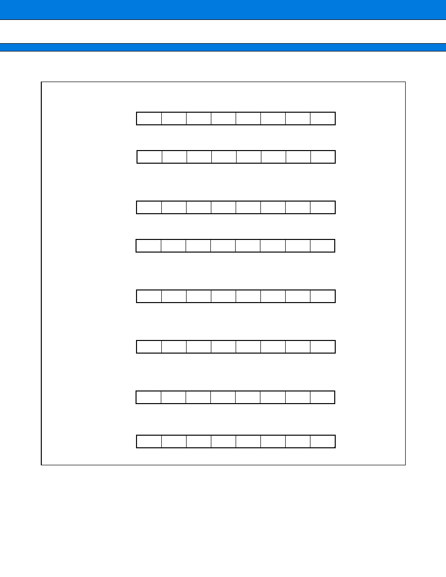
MB91350A Series
57
(2)Register list
∑ Up/down count resister (UDCR)
Up/down count resister ch0 (UDCR0)
Up/down count resister ch1 (UDCR1)
∑ Reload compare resister (RCR)
Reload compare resister ch0 (RCR0)
Reload compare resister ch1 (RCR1)
∑ Counter status register (CSR)
Counter status register ch(0, 1) (CSR0, 1)
∑ Counter control resister (CCRL)
Counter control resister ch(0, 1) (CCRL0, 1)
∑ Counter control resister (CCRH)
Counter control resister ch0 (CCRH0)
∑ Counter control resister ch1 (CCRH1)
7
6
5
4
3
2
1
0
D06
D07
D05
D04
D03
D02
D01
D00
15
14
13
12
11
10
9
8
D14
D15
D13
D12
D11
D10
D09
D08
7
6
5
4
3
2
1
0
D06
D07
D05
D04
D03
D02
D01
D00
15
14
13
12
11
10
9
8
D14
D15
D13
D12
D11
D10
D09
D08
7
6
5
4
3
2
1
0
CIT
CST
UDI
CM
OVF
UD
UD
UD
7
6
5
4
3
2
1
0
CTU
UC
RLD
UD
CGS
CGE
CGE
Reserved
15
14
13
12
11
10
9
8
CDC
M16
CFI
CLK
CM
CM
CES
CES
15
14
13
12
11
10
9
8
CDC
CFI
CLK
CM
CM
CES
CES
Reserved
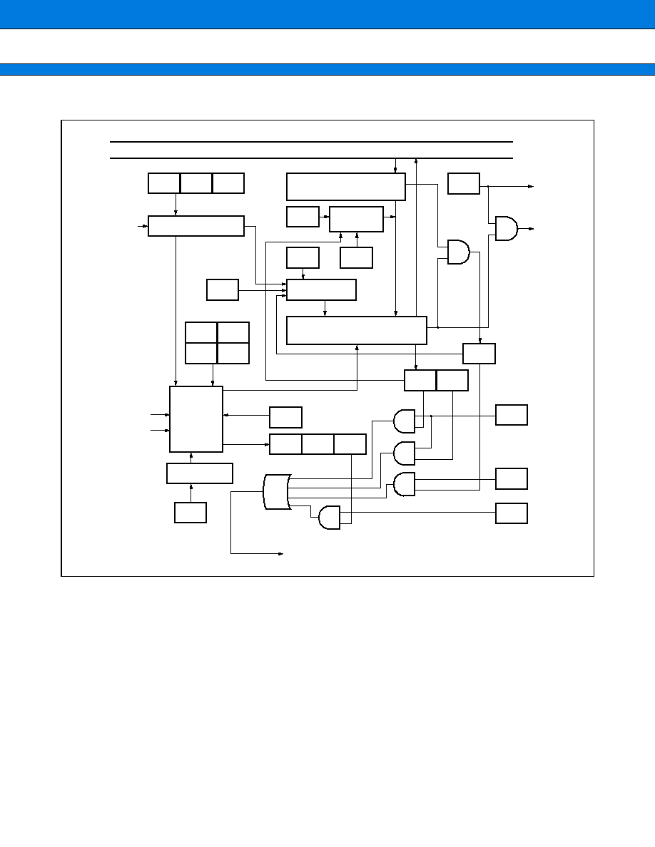
MB91350A Series
58
(3)Block diagram
CGE
CGE
CGS
CTU
UC
UD
CES
CES
CM
CLK
AIN0, AIN1
ZIN0, ZIN1
BIN0, BIN1
CM
CST
UD
UD
CDC
UD
OVF
CM
M16
Carry
UDI
CIT
CFI
RLD
8 bit
8 bit
Data bus
Edge/level detection
Up/down
count
clock
select
Prescaler
UDCR0(up/down
counter register ch0
Counter clear
Reload
control
RCR0(Reload
compare register ch0
Interrupt output
To ch1
Count
Clock
MB91350A Series
59
5.
16-bit Reload Timer
(1)Description
The 16-bit timer consists of a 16-bit down counter, 16-bit reload register, internal clock, clock generation prescaler,
and control register.
The clock source can be selected from among three internal clocks (prepared by frequency dividing the machine
clock by 2/8/32, and also by 64/128 only for ch3) and an external event.
The interrupt can be used to initiate DMA transfer.
The MB91F355A/MB91F356B/MB91355A/MB91354A/MB91V350A contain 4 channels of this timer.
(2)Register list
Control status register (TMCSR)
16-bit timer register(TMR)
16-bit reload register(TMRLR)
(ch3 only)
15
14
13
12
11
10
9
8
CSL2
CSL1
CSL0
Reserved
Reserved Reserved
7
6
5
4
3
2
1
0
OUTL
RELD
INTE
UF
CNTE
TRG
Reserved
15
0
15
0
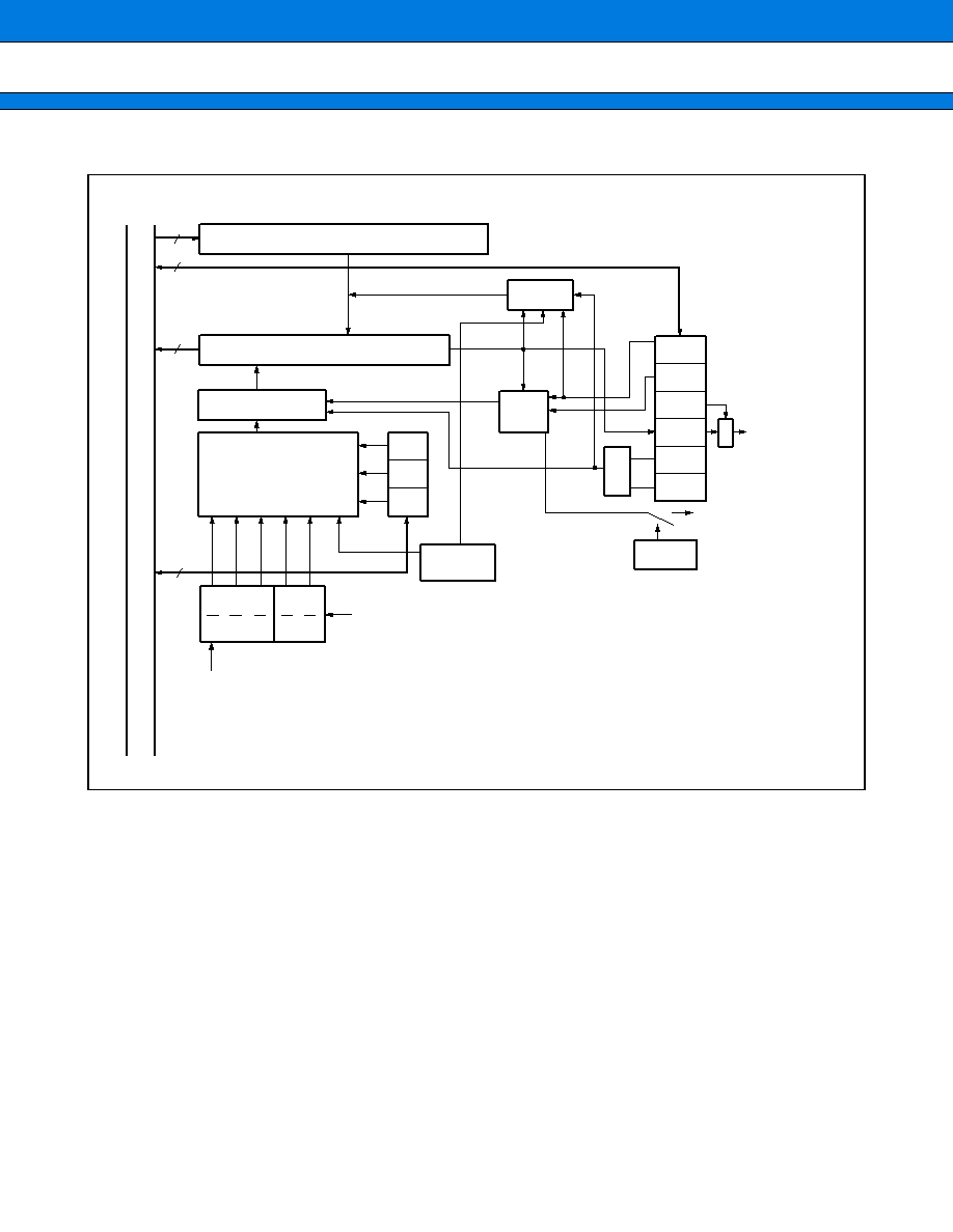
MB91350A Series
60
(3)Block diagram
RELD
OUTL
INTE
UF
CNTE
TRG
OUT
CTL.
CSL2
CSL1
CSL0
16
7
16
3
IN CTL.
TOE0 to 3
2
2
2
1
3
5
EXCK
IRQ
2
2
6
7
R
|
b
u
s
16-bit reload register (TMRLR)
16-bit timer register (TMR) UF
Reload
Clock selector
Re-trigger
Prescaler clear
Machine clock input
Bit in PFRP
Count enable
(ch3 only)
External timer output
(TOT0 to TOT3)
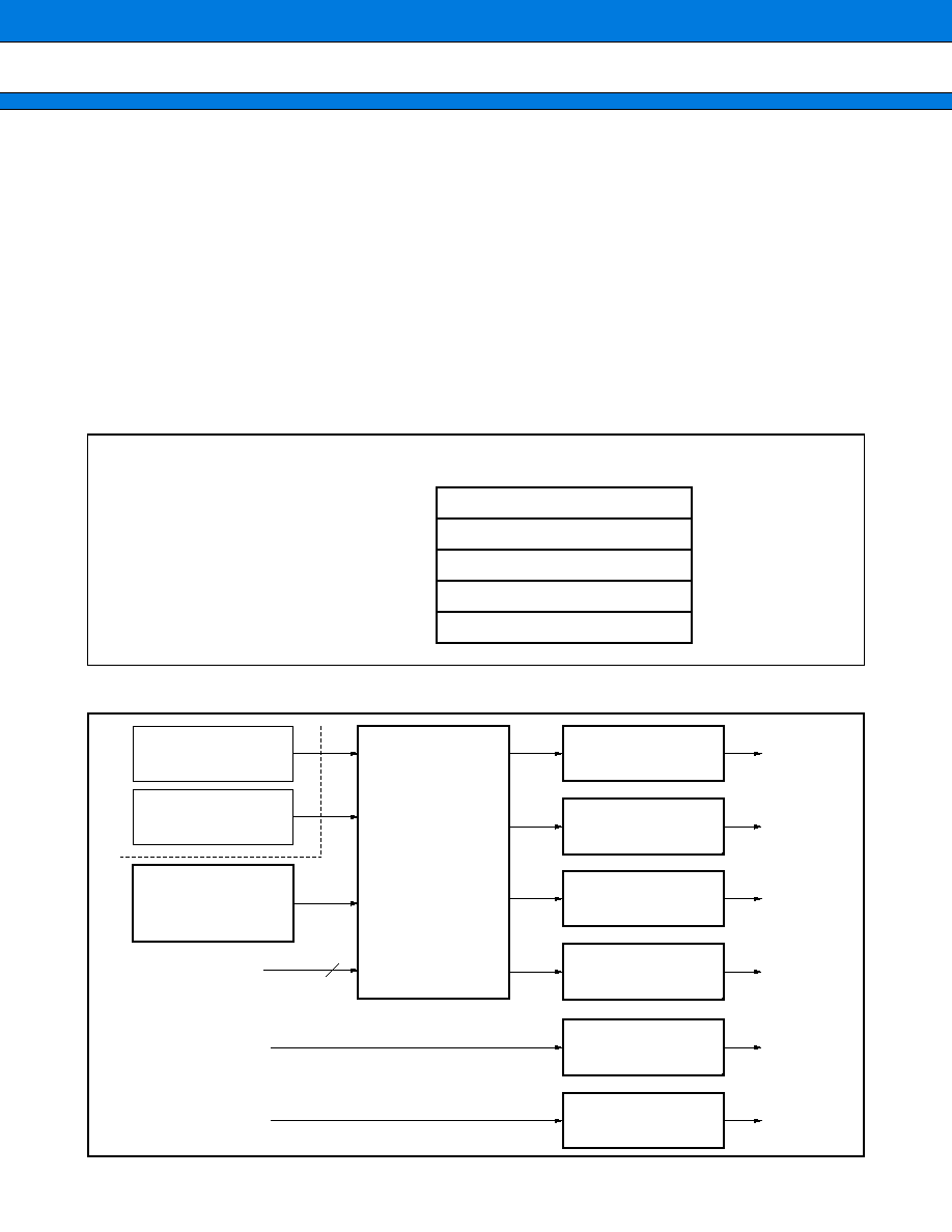
MB91350A Series
61
6.
PPG (Programable Pulse Generator)
The PPG can efficiently output highly precise PWM waveforms.
The MB91F355A/MB91F356B/MB91355A/MB91354A/MB91V350A contain 6 channels of PPG timer.
(1)Description
Each channel consists of a 16-bit down counter, 16-bit data register with cycle setting buffer, 16-bit compare
register with duty ratio setting buffer, and pin control unit.
The count clocks for the 16-bit down counter can be selected from the following 4 types :(peripheral clock
,
/
4,
/16,
/64)
The counter is initialized to "FFFF
H
" at a reset or counter borrow.
PPG outputs (PPG0 to PPG5) are provided for each channel.
(2)Register list
(3)Block diagram (overall configuration for 1 channel)
15 0
General control register 10 (GCN10)
General control register 20 (GCN20)
Timer register (PTMR0 to 5)
Cycle setting register (PCSR0 to 5)
Duty setting register (PDUT0)
4
PPG0
PPG4
PPG2
PPG1
PPG5
PPG3
16-bit reload timer ch0
16-bit reload timer ch1
General D/A control
ICR register 20
General D/A control
ICR register 10
(resource select)
TRG input
PPG timer ch4
TRG input
PPG timer ch2
External TRG0 to
TRG3
TRG input
PPG timer ch1
TRG input
PPG timer ch3
TRG input
PPG timer ch5
TRG input
PPG timer ch0
External TRG4
External TRG5
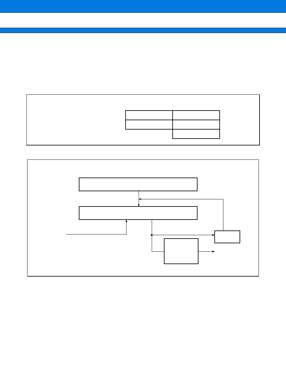
MB91350A Series
62
7.
U-Timer (16-bit timer for UART baud rate generation)
(1) Description
The U-Timer is a 16-bit timer for generating the baud rate for the UART. An arbitrary baud rate can be set
depending on the combination of the chip operating frequency and U-Timer reload value.
The MB91F355A/MB91F356B/MB91355A/MB91354A/MB91V350A contain 5 channels of this timer.
(2) Register list
(3) Block diagram
15 8 7 0
U-Timer Register (UTIM)
Reload Register (UTIMR)
U-Timer Control Register (UTIMC)
UTIMR (reload register)
UTIM (U-timer)
clock
load
underflow
to UART
control
f.f.
15
15
0
0
(Peripheral clock)
MB91350A Series
63
8.
UART
(1) Description
The UART is a serial I/O port for asynchronous (start-stop) or CLK synchronous communication. This module
has the features listed below. The MB91F355A/MB91F356B/MB91355A/MB91354A/MB91V350A contain 5
channels of UART.
∑ Full duplex double buffer
∑ Asynchronous (start-stop synchronized) or CLK synchronized transmission
∑ Supports multi-processor mode
∑ Completely programmable baud rate.
Arbitrary baud rate set by built-in timer (See the section for "U-Timer".)
∑ Variable baud rate can be input from an external clock.
∑ Error detection functions(parity, framing, overrun)
∑ Transmission signal format is NRZ
∑ UART Ch0 to Ch2 can start DMA transfer using interrupts (Ch3 and Ch4 cannot start DMA transfer).
∑ Capable of clearing DMAC interrupt source by writing to DRCL register
(2)Register list
Serial input register/serial output register (SIDR/SODR)
Serial status register(SSR)
Serial mode register
Serial control register(SCR)
DECL register (DRCL)
7
6
5
4
3
2
1
0
D6
D7
D5
D4
D3
D2
D1
D0
7
6
5
4
3
2
1
0
ORE
PE
FRE
RDRF
TDRE
BDS
RIE
TIE
7
6
5
4
3
2
1
0
MD0
MD1
CS0
7
6
5
4
3
2
1
0
P
PEN
SBL
CL
A/D
REC
RXE
TXE
7
6
5
4
3
2
1
0
MB91350A Series
64
(3) Block diagram
MD1
MD0
CS0
PEN
P
SBL
CL
A
/
D
REC
RXE
TXE
PE
ORE
FRE
RDRF
TDRE
BDS
RIE
TIE
R - bus
SIDR
SODR
Control signal
From U-Timer
External clock
SCK
Clock
selection
circuit
Receive status
decision circuit
For DMA
received error generating
signal (to DMAC)
Reception clock
Reception control
circuit
Start bit
detection circuit
Received bit
Counter
Received parity
Counter
RX shifter
RX
complete
Transmission clock
RX interrupt
(to CPU)
TX interrupt
(to CPU)
Transmission
control circuit
Transmission
start circuit
Sending bit
Counter
Sending parity
Counter
TX shifter
Start
transmis-
sion
SMR
Register
Control signal
SCR
Register
SSR
Register
SCK (clock)
SI (Receive data)
SO (Send data)
MB91350A Series
65
9.
Extended I/O Serial Interface (SIO)
(1) Description
This block is a serial I/O interface that allows data transfer using clock synchronization. It is composition of a
single 8-bit
◊
1 channel.
LSB-first or MSB-first transfer mode can be selected for data transfer.
The MB91F355A/MB91F356B/MB91355A/MB91354A/MB91V350A contain 3 channels of this SIO.
The serial I/O interface operates in 2 modes:
∑ Internal shift clock mode: Transfer data in synchronization with the internal clock.
∑ External shift clock mode: Transfer data in synchronization with the clock supplied via the external pin (SCK).
By manipulating the general-purpose port sharing the external pin (SCK) in this
mode, data can also be transferred by a CPU instruction.
(2) Register list
Serial mode control status register (SMCS)
SIO test resister(SES)
SDR (Serial Data Register)
SIO prescaler control register (CDCR)
DMAC interrupt source clear register (SRCL)
15
14
13
12
11
10
9
8
SMD1
SMD2
SMD0
SIE
SIR
BUSY
STOP
STRT
7
6
5
4
3
2
1
0
MODE
BDS
15
14
13
12
11
10
9
8
TST1
TST0
7
6
5
4
3
2
1
0
D6
D7
D5
D4
D3
D2
D1
D0
15
14
13
12
11
10
9
8
MD
DIV3
DIV2
DIV1
DIV0
7
6
5
4
3
2
1
0
MB91350A Series
66
(3)Block diagram
SI5 to SI7
SO5 to SO7
SCK5 to SCK7
SMD2 SMD1 SMD0
SIE
SIR
BUSY STOP STRT MODE BDS
2
1
0
SCE
(MSB fast) D0 to D7
(MSB fast) D0 to D7
SDR (Serial Data Register)
Internal clock
Internal data bus
Select transmitting direction
Read
write
Control circuit
Shift clock counter
Interrupt
request
Internal data bus
Initial Value
PFR
Register
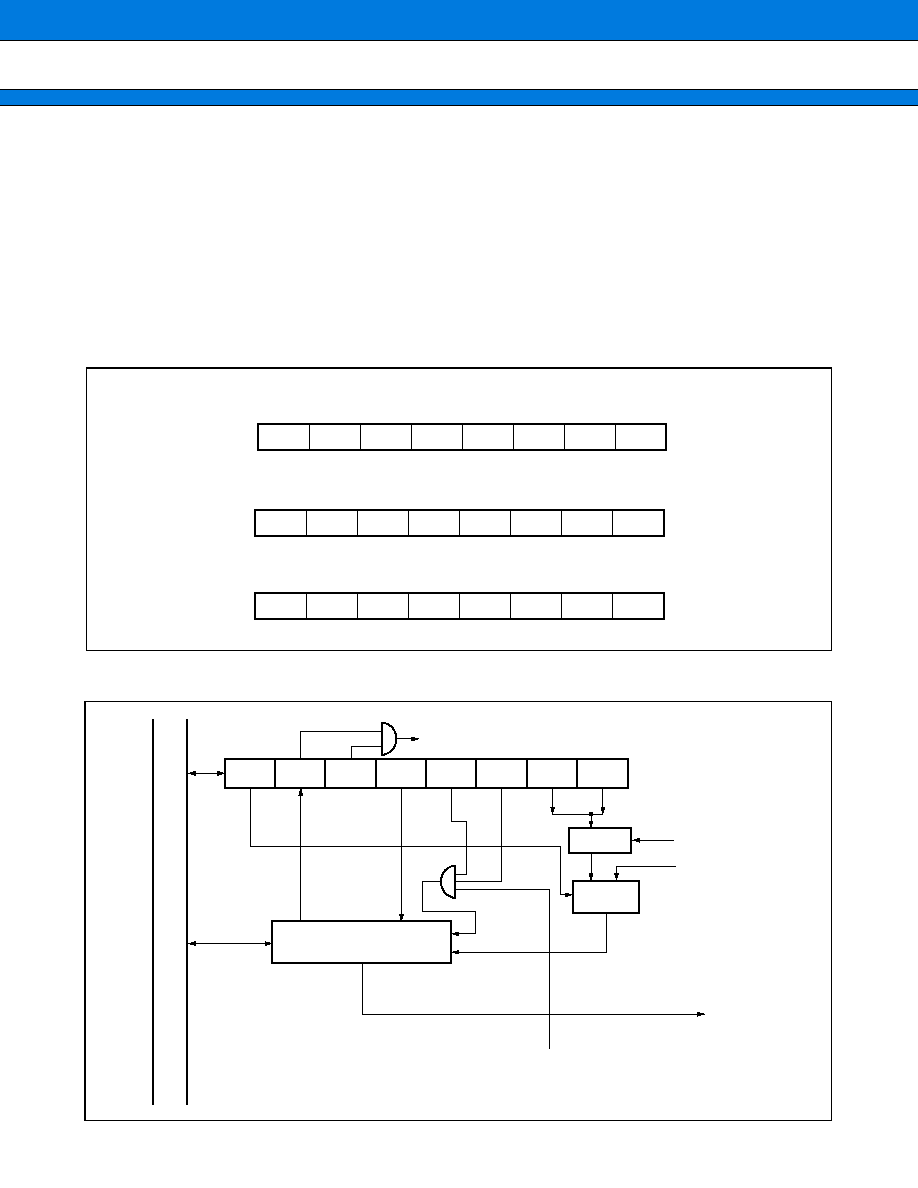
MB91350A Series
67
10. 16-bit free-run timer
(1)Description
The 16-bit free-running timer consists of a 16-bit up counter, control register, and status register. The count
values of this timer are used as the base timer for the output compares and input capture modules.
∑ Four count clock frequencies are available.
∑ An interrupt can be generated at a counter overflow.
∑ The counter can be initialized upon a match with compare register 0 of the output compare unit, depending
on the mode.
(2)Register list
(3)Block diagram
Timer data register (upper) (TCDT)
Timer data register (lower) (TCDT)
Timer control status register (lower) (TCCS)
15
14
13
12
11
10
9
8
T14
T15
T13
T12
T11
T10
T9
T8
7
6
5
4
3
2
1
0
T06
T07
T05
T04
T03
T02
T01
T00
7
6
5
4
3
2
1
0
IVF
ECLK
IVFE
STOP
MODE
CLR
CLK1
CLK0
ECLK
IVF
IVFE
STOP
MODE
CLR
CLK1
CLK0
FRCK
R-b
us
Interrupt
Timer data register
(TCDT)
Divider
Clock
select
to internal circuit (T15 to T00)
Comparator 0
Clock
MB91350A Series
68
11. Input Capture
(1) Description
This module detects a rising or falling edge or both edges of an external input signal and stores the 16-bit free-
running timer value in a register.
This module stores the 16-bit free-running timer value in a register. In addition, the module can generate an
interrupt upon detection of an edge.
The input capture module consists of input capture data registers and a control register.
Each input capture unit has a corresponding external input pin.
∑ The detection edge of an external input can be selected from among 3 types.
Rising edge
Falling edge
Both edges
∑ An interrupt can be generated upon detection of a valid edge of an external input.
(2) Register list
Input capture data register (upper) (IPCP)
Input capture data register (lower) (IPCP)
Capture control register (ICS23)
Capture control register (ICS01)
15
14
13
12
11
10
9
8
CP14
CP15
CP13
CP12
CP11
CP10
CP09
CP08
7
6
5
4
3
2
1
0
CP06
CP07
CP05
CP04
CP03
CP02
CP01
CP00
7
6
5
4
3
2
1
0
ICP2
ICP3
ICE3
ICE2
EG31
EG30
EG21
EG20
7
6
5
4
3
2
1
0
ICP0
ICP1
ICE1
ICE0
EG11
EG10
EG01
EG00
MB91350A Series
69
(3) Block diagram
EG11
EG10
EG01
EG00
EG31
EG30
EG21
EG20
ICP1
ICP0
ICE1
ICE0
ICP3
ICP2
ICE3
ICE2
R-b
us
16-bit timer counter value
(T15 to T00)
Input capture data register
ch (0, 2)
16-bit timer counter value
(T15 to T00)
Input capture data register
ch (1, 3)
Edge
detection
Edge
detection
IN0, IN2
Input pin
IN1, IN3
Input pin
Interrupt
Interrupt
MB91350A Series
70
12. Output Compare
(1) Description
The output compare module consists of 16-bit compare registers, compare output latch, and control register.
When the 16-bit free-running timer value matches the compare register value, the output level is inverted and
an interrupt is issued.
The MB91F355A/MB91F356B/MB91355A/MB91354A/MB91V350A contain 8 channels of this block.
This module has the features listed below.
∑ Capable of using the 8 compare registers independently. Output pins and interrupt flags corresponding to the
compare registers
∑ A pair of compare registers can be used to control output pins. Using tow compare registers to invert output pins
∑ Capable of setting the initial value for each output pin.
∑ Interrupts can be generated upon a compare match.
∑ The ch0 compare register is used as the compare clear register for the 16-bit free-running timer.
(2)Register list
Output compare register(upper) (OCCP)
Output compare register(lower) (OCCP)
Output control register(upper) (OCS)
Output control register(lower) (OCS)
15
14
13
12
11
10
9
8
C14
C15
C13
C12
C11
C10
C09
C08
7
6
5
4
3
2
1
0
C06
C07
C05
C04
C03
C02
C01
C00
15
14
13
12
11
10
9
8
CMOD
OTD1
OTD0
7
6
5
4
3
2
1
0
ICP0
ICP1
ICE1
ICE0
CST1
CST0
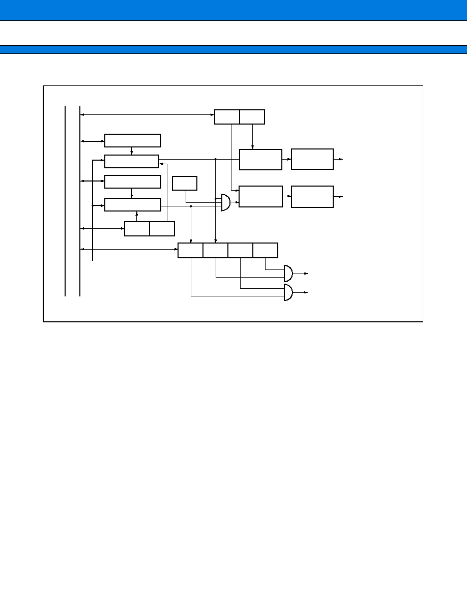
MB91350A Series
71
(3) Block diagram
ICP1
ICP0
ICE1
ICE0
OTD1
OTD0
CST1
CST0
CMOD
OTE0, OTE2,
OTE4, OTE6
R-b
us
OTE1, OTE3,
OTE5, OTE7
(Only ch0 is used as a free running timer
clear register.)
Output compare
register
Compare circuit
Output compare
register
Compare circuit
16-bit free-run timer
Interrupt output
Compare
Output latch
Compare
Output latch
OTE0 and OTE7 exist in PFRO.
There is in PFRO.
Output
Interrupt output
Output

MB91350A Series
72
13. I
2
C Interface
(1) Description
The I
2
C interface is a serial I/O port supporting the Inter-IC bus, operating as a master/slave device on the I
2
C
bus. It has the following features
∑ Master/slave sending and receiving
∑ Arbitration function
∑ Clock sync function
∑ Slave address and general call address detection function
∑ Ditecting function of transmitting direction
∑ Repeated start condition generation and detection function
∑ Bus error detection function
∑ 10-bit/7-bit slave address
∑ Slave address receive acknowledge control when in master mode
∑ Support for composite slave addresses
∑ Capable of interruption when a transmission or bus error occurs
∑ Standard mode (Max 100K bps)/High speed mode (Max 400K bps) supported
MB91350A Series
73
(2)Register list
Bus control register(IBCR)
Bus status register(IBSR)
10-bit slave address resister (ITBA)
10-bit slave address mask resister(ITMK)
7-bit slave address resister (ISBA)
7-bit slave address mask resister (ISMK)
Data register (IDAR)
Clock control register (ICCR)
Clock disable register (IDBL)
15
14
13
12
11
10
9
8
BER
BEIE
SCC
MSS
ACK GCAA INTE
INT
7
6
5
4
3
2
1
0
BB
RSC
AL
LRB
TRX
AAS
GCA
ADT
15
14
13
12
11
10
9
8
TA9
TA8
7
6
5
4
3
2
1
0
TA7
TA6
TA5
TA4
TA3
TA2
TA1
TA0
15
14
13
12
11
10
9
8
ENTB
RAL
TM9
TM8
7
6
5
4
3
2
1
0
TM7
TM6
TM5
TM4
TM3
TM2
TM1
TM0
7
6
5
4
3
2
1
0
SA6
SA5
SA4
SA3
SA2
SA1
SA0
15
14
13
12
11
10
9
8
ENSB
SM6
SM5
SM4
SM3
SM2
SM1
SM0
7
6
5
4
3
2
1
0
D7
D6
D5
D4
D3
D2
D1
D0
15
14
13
12
11
10
9
8
TEST
EN
CS4
CS3
CS2
CS1
CS0
7
6
5
4
3
2
1
0
DBL
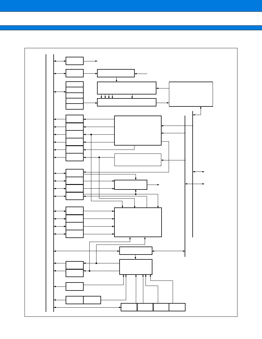
MB91350A Series
74
(3) Block diagram
ICCR
EN
IDBL
DBL
ICCR
IBSR
BB
RSC
LRB
Last Bit
TRX
ADT
AL
IBCR
BER
BEIE
INTE
INT
IBCR
SCC
MSS
ACK
GCAA
IBSR
ISMK
ITMK
IDAR
AAS
GCA
FNSB
ENTB
RAL
ITBA
ITMK
ISBA
ISMK
CS4
CS3
CS2
CS1
CS0
2 3 4 5
32
Sync
CLKP
First Byte
IRQ
SCLI
SCLO
SDA
SDAO
Operation enable
Clock enable
Clock divide 2
Clock selector2 (1/12)
Bus busy
Start
Sending/
receiving
Start stop condition
generation
Arbitration lost detection
Interrupt request
Start
Master
ACK enable
ACK enable
Slave
Global call
Slave address
compare
End
Error
Shift clock edge
changing timing
Start stop condition
detection
Generating shift clock
R-bus
MB91350A Series
75
14. A/D Converter
(1) Description
The A/D converter converts the analog input voltage into a digital value. It has the following features:
∑ Conversion time: 1.48
µ
s minimum per channel
∑ Employing serial/parallel conversion type for sample & hold circuit
∑ 10-bit resolution (switchable between 8 and 10 bits)
∑ Program selection of the analog input from among 12 channels
∑ Conversion mode
Single conversion mode : Convert 1 selected channel
Scan conversion mode
: Scan up to 4 channels.
∑ Converted data is stored in the data buffer.
∑ An interrupt request to the CPU can be generated upon completion of A/D conversion. The interrupt can be
used to start DMA transfer.
∑ The startup source can be selected from among software, external trigger (falling edge), and reload timer ch2
(rising edge).
(2) Register list
ADCS1
ADCS2
15
0
ADTL0
ADTH0
ADTL2
ADTL1
ADTH1
ADTH2
ADTL3
ADTH3
8 7
Control status register (ADCS2/ADSC1)
Conversion time setting resister (ADCT)
Converted data register 0 (ADTH0/ADTL0)
Converted data register 1 (ADTH1/ADTL1)
Converted data register 2 (ADTH2/ADTL2)
Converted data register 3 (ADTH3/ADTL3)
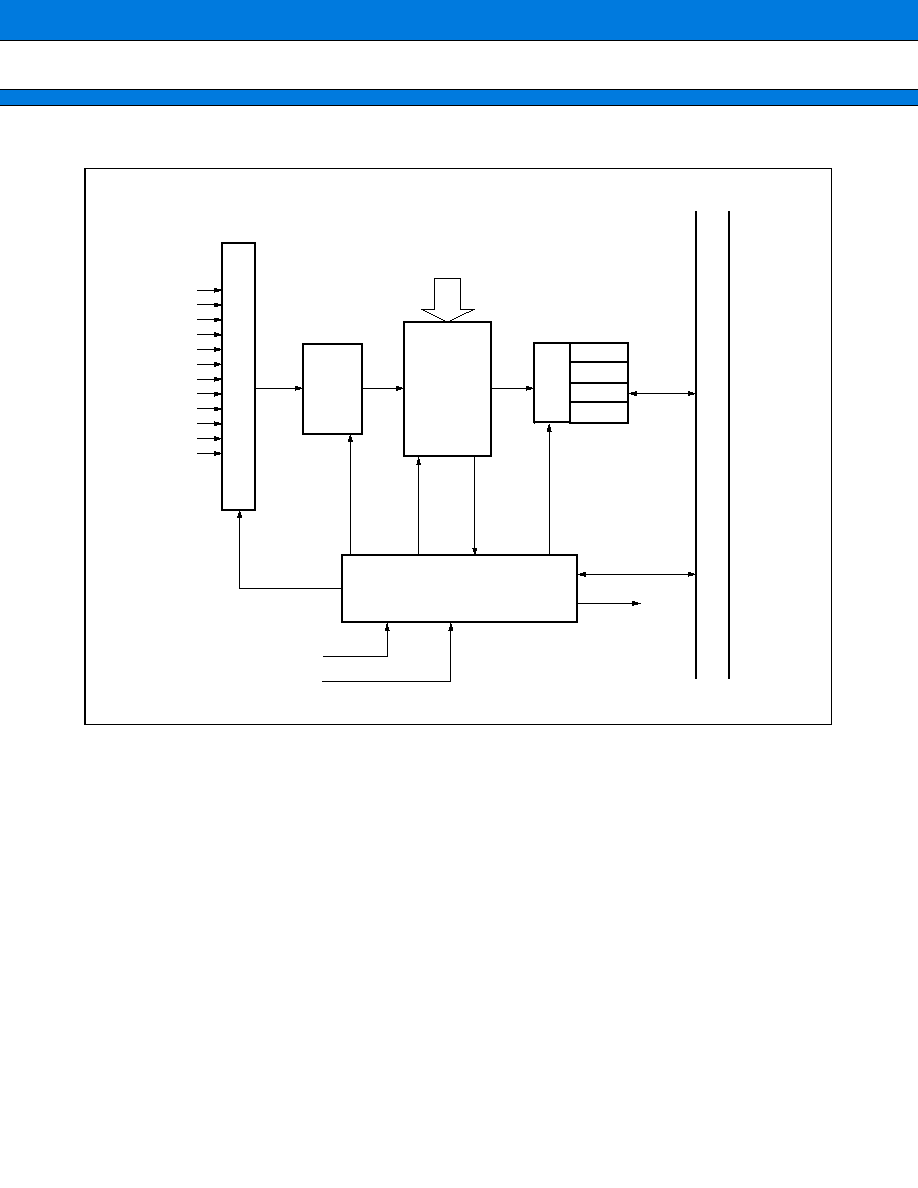
MB91350A Series
76
(3) Block diagram
AV
CC
, AVRH, AV
SS
/AVRL
AN0
AN1
AN2
AN3
AN4
AN5
AN6
AN7
AN8
AN9
AN10
AN11
M
P
X
M
P
X
S/H
ADT0
ADT1
ADT2
ADT3
10 bit
A/D
Converter
R-bus
Control logic
Interrupt
16-bit reload timer ch2
External input
Analog input
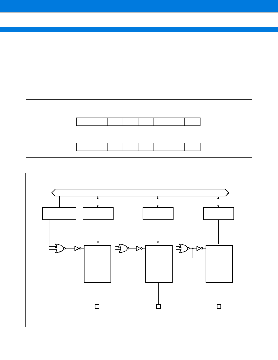
MB91350A Series
77
15. 8-bit D/A Converter
(1) Description
This block contains 2 channels of 8-bit D/A converters. The D/A converter register can be used to control the
independent output of each channel. The block has the following features.
∑ Power saving function
∑ 3.3 V Interface
(2) Register list
(3) Block diagram
D/A data register 0 to 2(DADR0 to DADR2)
D/A control register 0 to 2 (DACR0 to DACR2)
7
6
5
4
3
2
1
0
DA6
DA7
DA5
DA4
DA3
DA2
DA1
DA0
7
6
5
4
3
2
1
0
DAE
DAE0
PD
R-bus
DAE1
STOP
STOP
PD
D/A
D/A
DAE2
STOP
PD
D/A
D/A control
D/A
converter
D/A
converter
D/A output 0
D/A output 1
D/A
converter
D/A output 2

MB91350A Series
78
16. DMAC (DMA Controller)
(1) Description
This module realize direct memory access (DMA) transfer with the FR family device.
DMA transfer controlled by this module enables many types of data transfer to be performed at high speed
without CPU intervention, thereby improving system performance.
∑ Hardware configuration
This model consists mainly of the following components:
∑ Independent DMA channels
◊
5 channels
∑ 5 channels independent access control circuits
∑ 32-bit address register (Supports reloading: 2 per channel)
∑ 16-bit transfer count register (Supports reloading: 1 per channel)
∑ 4-bit block count register (1 per channel)
∑ External transfer request input pins: DREQ0, DREQ1, DREQ2 (ch0, ch1, ch2 only)
∑ External transfer request acceptance output pins: DACK0, DACK1, DACK2 (ch0, ch1,ch2 only)
∑ DMA end output pins: DEOP0, DEOP1, DEOP2 (ch0, ch1, ch2 only)
∑ (ch3 only) fly-by transfer (memory to I/O, I/O to memory)
∑ 2-cycle transfer
∑ Main function
This module has the following major functions for data transfer:
∑ Supports independent data transfer for multiple channels (5 channels)
(1) Priority order (ch0
>
ch1
>
ch2
>
ch3
>
ch4)
(2) Order can be reversed for ch0 and ch1
(3) DMAC activation triggers
∑ External dedicated pin input (edge detection/level detection: ch0 to ch2 only)
∑ Internal peripheral request (Interrupt request sharing, including external interrupts)
∑ Software request (register write)
(4) Transmission mode
∑ Demand transfer, burst transfer, step transfer, or block transfer
∑ Addressing mode: 32-bit full addressing (increment, decrement, or fixed)
(address increment can be in the range - 255 to + 255)
∑ Data length: Byte, halfword, or word
∑ Single-shot or reload operation selectable
MB91350A Series
79
(2) Register Description
31 16 15 0
Ch0 control/status
register A (DMACA0)
register B (DMACB0)
Ch1 control/status
register A (DMACA1)
register B (DMACB1)
Ch2 control/status
register A (DMACA2)
register B (DMACB2)
Ch3 control/status
register A (DMACA3)
register B (DMACB3)
Ch4 control/status
register A (DMACA4)
register B (DMACB4)
Overall control register
(DMACR)
Ch0 transfer source address register
(DMASA0)
(DMADA0)
Ch1 transfer source address register
(DMASA1)
(DMADA1)
Ch2 transfer source address register
(DMASA2)
(DMADA2)
Ch3 transfer source address register
(DMASA3)
(DMADA3)
Ch4 transfer source address register
(DMASA4)
(DMADA4)
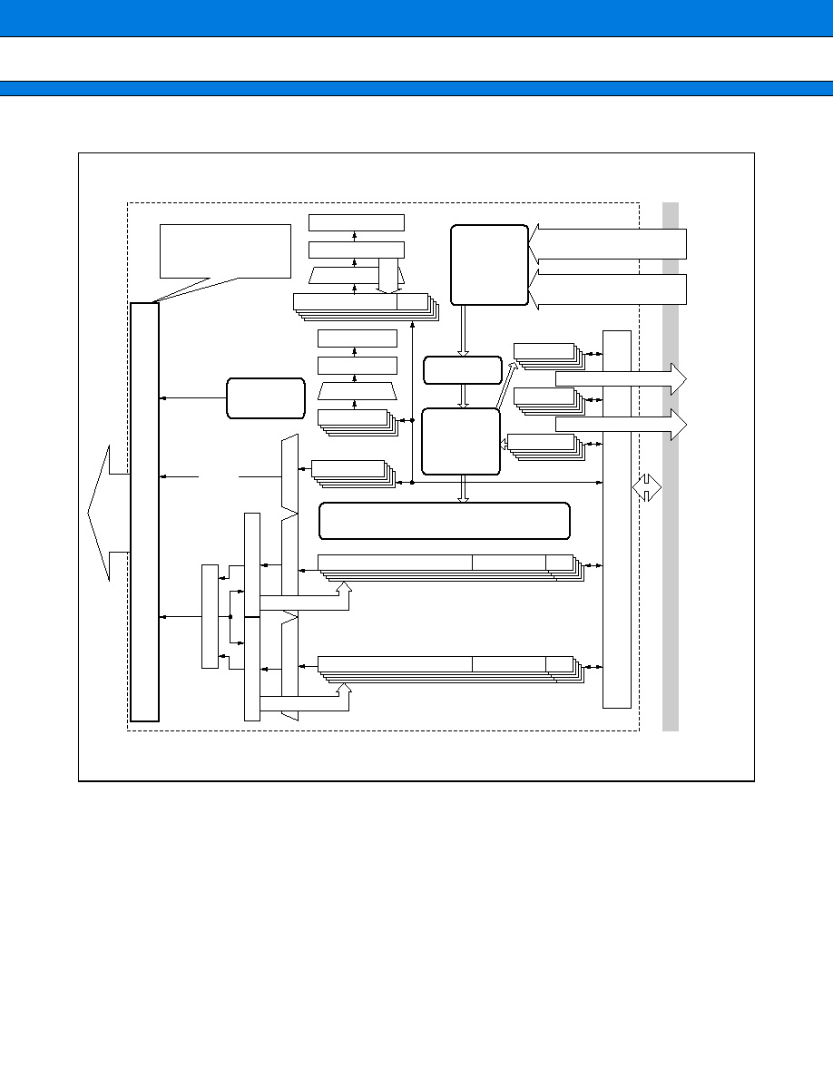
MB91350A Series
80
(3) Block diagram
Read
Write
DDNO
BLK register
DDNO register
DTCR
DSS [3:0]
ERIR, EDIR
TYPE, MOD, WS
IRQ
[4:0]
MCLREQ
X-bus
DADM, DASZ [7:0] DADR
SADM, SASZ [7:0] SADR
DMA transfer request
to bus controller
Read/write
control
T
o
bus
con-
troller
Bus control block
Access
Address
Address counter
Counter buffer
C
ounter buffer
Selector
Selector
Write back
Selector
Buffer
Counter
Selector
Write
back
DTC two-stage register
Buffer
Counter
Selector
DMA start
source select
circuit & request
acceptance
control
Priority
circuit
Status
transition
circuit
DMA control
DSAD two-stage register
DDAD two-stage register
Bus control block
Peripheral start request/
Stop input
External pin start
request/stop input
To interrupt controller
Clear peripheral interrupt
5-channel DMAC block diagram
Write back
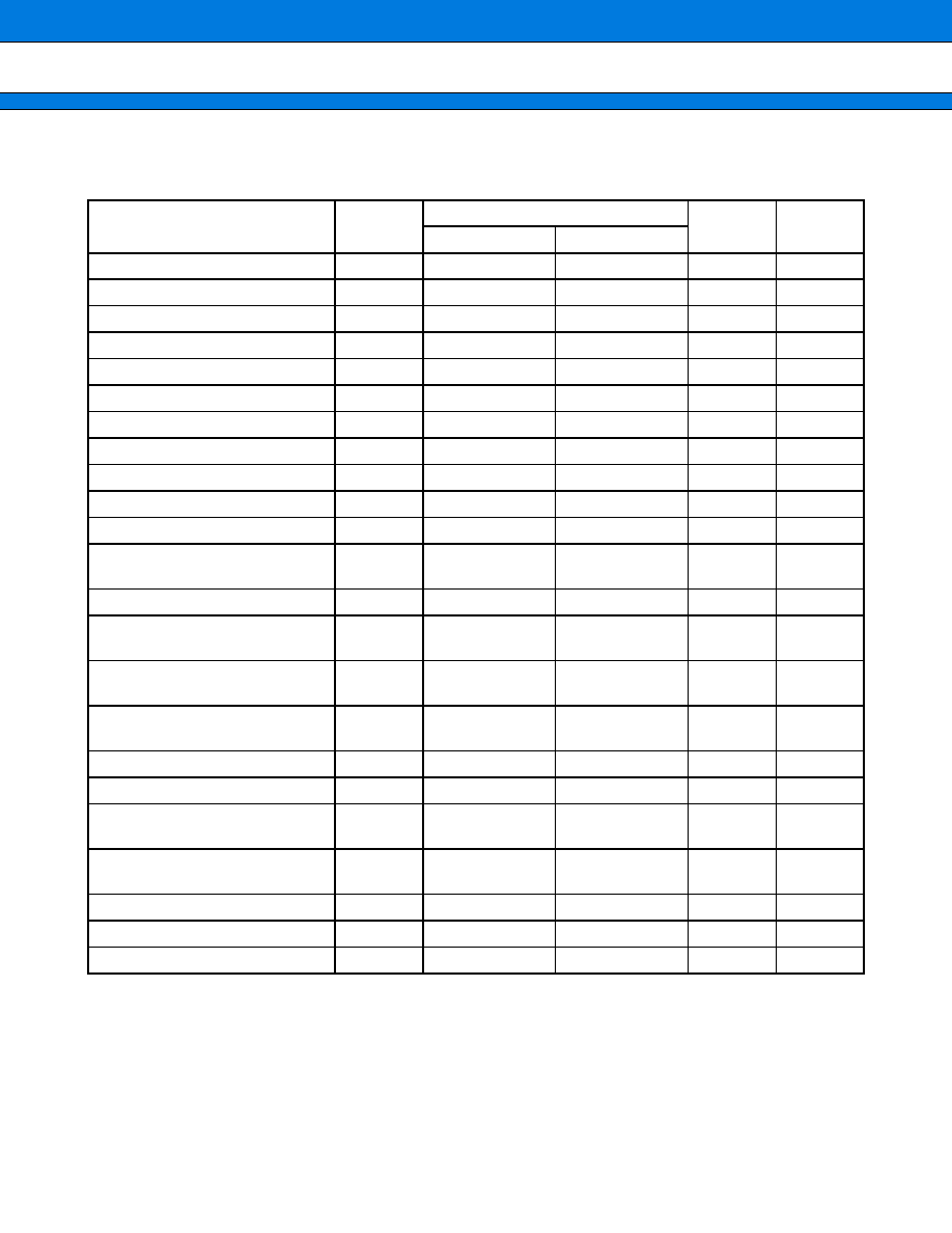
MB91350A Series
81
ELECTRICAL CHARACTERISTICS
1.
Abusolute Maximum Rating
*1 : The parameter is based on V
SS
=
DA
VS
=
AV
SS
=
0 V.
*2 : V
CC
must not be lower than V
SS
- 0.3 V.
*3 : Be careful not to exceed "V
CC
+ 0.3 V", for example, when the power is turned on.
*4 : The maximum output current is the peak value for a single pin.
*5 : The average output current is the average current for a single pin over a period of 100 ms.
*6 : The total average output current is the average current for all pins over a period of 100 ms.
Parameter
Symbol
Rating
Unit
Remarks
Min
Max
Power supply voltage*
1
V
CC
V
SS
-
0.5
V
SS
+
4.0
V
*2
Analog power supply voltage*
1
DA
VC
V
SS
-
0.5
V
SS
+
4.0
V
*3
Analog power supply voltage*
1
AV
CC
V
SS
-
0.5
V
SS
+
4.0
V
*3
Analog reference voltage*
1
AVRH
V
SS
-
0.5
V
SS
+
4.0
V
*3
Input voltage*
1
V
I
V
SS
-
0.5
V
CC
+
0.5
V
*8
Input voltage (Nch open-drain) *
1
V
IND
V
SS
-
0.5
V
SS
+
5.5
V
*8
Analog pin input voltage*
1
V
IA
V
SS
-
0.5
AV
CC
+
0.5
V
*8
Output voltage*
1
V
O
V
SS
-
0.5
V
CC
+
0.5
V
Maximum clamp current
I
CLAMP
-
2.0
+
2.0
mA
*7
Total maximum clamp current
|I
CLAMP
|
20
mA
*7
"L" level maximum output current
I
OL
10
mA
*4
"H" level maximum output current
(Nch open-drain)
I
OLND
20
mA
"L" level average output current
I
OLAV
8
mA
*5
"H" level average output current
(Nch open-drain)
I
OLAVND
15
mA
"L" level total maximum output
current
I
OL
100
mA
"L" level total average output
current
I
OLAV
50
mA
*6
"H" level maximum output current
I
OH
-
10
mA
*4
"H" level average output current
I
OHAV
-
4
mA
*5
"H" level total maximum output
current
I
OH
-
50
mA
"H" level total average output
current
I
OHAV
-
20
mA
*6
Power consumption
P
D
850
mW
Operating temperature
T
a
-
40
+
85
∞
C
Storage temperature
T
STG
+
125
∞
C
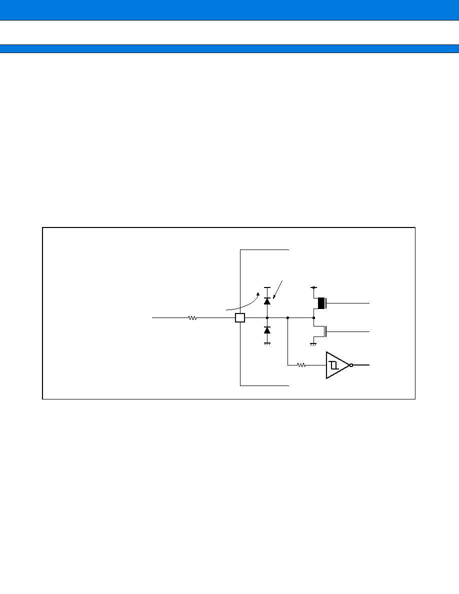
MB91350A Series
82
*7 :
∑
Relevant pins: Port2, 3, 4, 5, 6, 8, 9, A, B, C, G, H, I, J, K, M, N, O, P, and AN (A/D input)
∑
Use within recommended operating conditions.
∑
Use at DC voltage (current).
∑
The + B signal should always be applied a limiting resistance placed between the + B signal and
the microcontroller.
∑
The value of the limiting resistance should be set so that when the + B signal is applied the input current to
the microcontroller pin does not exceed rated values, either instantaneously or for prolonged periods.
∑
Note that, when the microcontroller drive current is low as in low power consumption mode, the + B input
potential can increase the potential at the V
CC
pin via a protective diode, possibly affecting other devices.
∑
Note that, if the + B input exists when the microcontroller is off (not fixed at 0 V), power is supplied through
the pin, possibly causing the microcontroller to operate imperfectly.
∑
Note that, if the + B input exists when the power supply is turned on, power is supplied through the pin,
possibly resulting in a power-supply voltage at which a power-on reset does not work.
∑
Be careful not to let the + B input pin open.
∑
Note that the analog I/O pins (such as the LCD drive and comparator input pins) other than the A/D input pin
cannot input + B.
∑
Sample recommended circuits:
*8: V
I
should not exceed the specified ratings. However, if the maximum current to/from an input is limited by some
means with external components, the I
CLAMP
rating supersedes the V
I
rating.
WARNING: Semiconductor devices can be permanently damaged by application of stress (voltage, current,
temperature, etc.) in excess of absolute maximum ratings. Do not exceed these ratings.
∑ Input/output equivalent circuits
Vcc
Pch
R
Nch
Protective diode
Limiting
resistance
+ B input (0 V to 16 V)
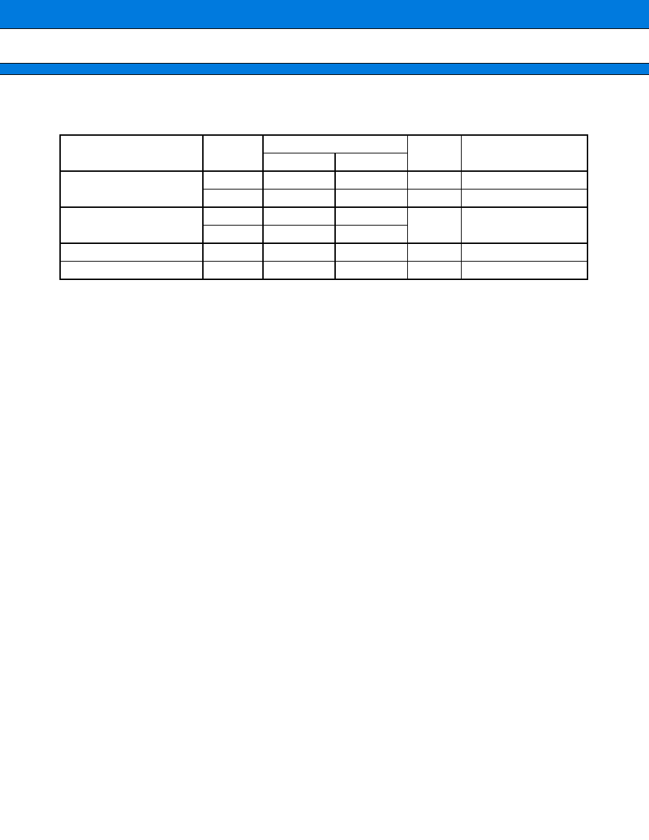
MB91350A Series
83
2.
Recommended Operating Conditions
(V
SS
=
DA
VS
=
AV
SS
=
0 V)
WARNING: The recommended operating conditions are required in order to ensure the normal operation of the
semiconductor device. All of the device's electrical characteristics are warranted when the device is
operated within these ranges.
Always use semiconductor devices within their recommended operating condition ranges. Operation
outside these ranges may adversely affect reliability and could result in device failure.
No warranty is made with respect to uses, operating conditions, or combinations not represented on
the data sheet. Users considering application outside the listed conditions are advised to contact their
FUJITSU representatives beforehand.
Parameter
Symbol
Value
Unit
Remarks
Min
Max
Power supply voltage
V
CC
3.0
3.6
V
At normal operating
V
CC
3.0
3.6
V
hold RAM status at stop
Analog power supply voltage
DA
VC
V
SS
-
0.3
V
SS
+
3.6
V
AV
CC
V
SS
-
0.3
V
SS
+
3.6
Analog reference voltage
AVRH
AV
SS
AV
CC
V
Operating temperature
Ta
-
40
+
85
∞
C
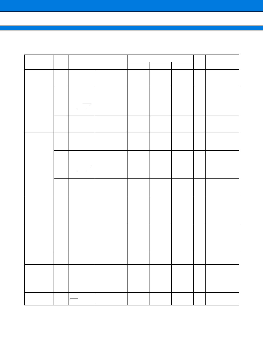
MB91350A Series
84
3.
DC Characteristics
(V
CC
=
3.0 V to 3.6 V, V
SS
=
DA
VS
=
AV
SS
=
0 V, Ta
=
-
40
∞
C to
+
85
∞
C)
(Continued)
Parameter
Sym-
bol
Pin
Conditions
Value
Unit
Remarks
Min
Typ
Max
"H" level
input voltage
V
IH
Port 2, 3, 4,
5, 6, 9, A, B,
C
V
CC
◊
0.65
V
CC
-
0.3
V
V
IHS
Port 8, G, H,
I, M, N, O, P,
MD0, MD1,
MD2, INIT,
NMI
V
CC
◊
0.8
V
CC
-
0.3
V
Hysteresis
input
V
IHST
Port J, K, L
V
CC
◊
0.8
5.25
V
Hysteresis input
with stand
voltage of 5 V
"L" level
input voltage
V
IL
Port 2, 3, 4,
5, 6, 9, A, B,
C
V
SS
V
CC
◊
0.25
V
V
ILS
Port 8, G, H,
I, M, N, O, P,
MD0, MD1,
MD2, INIT,
NMI
V
SS
V
CC
◊
0.2
V
Hysteresis input
V
ILST
Port J, K, L
V
SS
V
CC
◊
0.2
V
Hysteresis input
with stand
voltage of 5 V
"H" level
output voltage
V
OH
Port 2, 3, 4,
5, 6, 8, 9, A,
B, C, G, H, I,
J, K, M, N,
O, P
V
CC
=
3.0 V
I
OH
=
-
4.0 mA
V
CC
-
0.5
V
CC
V
"L" level
output voltage
V
OL1
Port 2, 3, 4,
5, 6, 8, 9, A,
B, C, G, H, I,
J, K, M, N,
O, P
V
CC
=
3.0 V
I
OL
=
4.0 mA
V
SS
0.4
V
V
OL2
Port L
V
CC
=
3.0 V
I
OL
=
15.0 mA
V
SS
0.4
V
Nch open-drain
Input leak
current
(High-Z
output Leak-
age current)
I
LI
All input pin
V
CC
=
3.6 V
0<V
I
<V
CC
-
5
+
5
µ
A
Pull-up
resistance
R
UP
setting pin
INIT, Pull up
V
CC
=
3.6 V
V
I
=
0.45 V
25
50
200
k

MB91350A Series
85
(Continued)
(V
CC
=
3.0 V to 3.6 V, V
SS
=
DA
VS
=
AV
SS
=
0 V, Ta
=
-
40
∞
C to
+
85
∞
C)
Parameter
Sym-
bol
Pin
Conditions
Value
Unit
Remarks
Min
Typ
Max
Power
supply
current
I
CC
V
CC
f
C
=
12.5 MHz
V
CC
=
3.3 V
160
220
mA
Multiply by 4
CLKB : 50 MHz
CLKT : 25 MHz
When operating at
25 MHz
I
CCS
f
C
=
12.5 MHz
V
CC
=
3.3 V
100
140
mA
Sleep
When operating at
25 MHz
I
CCH
Ta
=
+
25
∞
C
V
CC
=
3.3 V
1
100
µ
A
at stop
I
CCL
Ta
=
+
25
∞
C
f
C
=
32.768 kHz
V
CC
=
3.3 V
0.3
3.0
mA
Sub RUN
CLKB : 32.768 kHz
CLKT : 32.768 kHz
When operating at
32.768 kHz
I
CCLS
Ta
=
+
25
∞
C
f
C
=
32.768 kHz
V
CC
=
3.3 V
0.2
2.0
mA
Sub sleep
When operating at
32.768 kHz
I
CCT
Ta
=
+
25
∞
C
f
C
=
32.768 kHz
V
CC
=
3.3 V
5
120
µ
A
at watch mode
operating
(Main Off, STOP)
Input
capacitance
C
IH
Other than
V
CC
, V
SS
,
AV
CC
, AV
SS
,
DA
VC
, DA
VS
5
15
pF
MB91350A Series
86
4.
AC Characteristics
(1) Clock timing
(V
CC
=
3.0 V to 3.6 V, V
SS
=
DA
VS
=
AV
SS
=
0 V, Ta
=
-
40
∞
C to
+
85
∞
C)
* : The values assume a gear cycle of 1/16.
Parameter
Sym-
bol
Pin
Conditions
Value
Unit
Remarks
Min
Typ
Max
Clock
frequency
f
C
X0
X1
10
12.5
MHz
Main PLL
(When operating at
max internal frequency
(50 MHz)
=
12.5 MHz
self-oscillation with
◊
4
PLL)
Clock cycle time
t
C
X0
X1
80
100
ns
Clock
frequency
f
C
X0
X1
10
25
MHz
Main self-oscillation
(frequency-halved
input)
Internal operating
clock frequency
f
CP
When a minimum
value of 12.5 MHz
is input as the X0
clock frequency
and
◊
4 multiplica-
tion is set for the
PLL of the oscillator
circuit
2.94*
50
MHz CPU
f
CPP
2.94*
25
MHz Peripheral
f
CPT
2.94*
25
MHz External bus
Internal operating
clock cycle time
t
CP
20
340*
ns
CPU
t
CPP
40
340*
ns
Peripheral
t
CPT
40
340*
ns
External bus
Clock
frequency
f
C
X0A
X1A
30
32.768
35
kHz
SUB
self-oscillation
Clock cycle time
t
C
X0A
X1A
28.6
30.51
33.3
µ
s
Input clock palse
width
X0
X1
P
WH
/tc
P
WL
/tc
40
60
%
Internal operating
clock frequency
f
CP
,
f
CPP
,
f
CPT
When a standard
value of 32.768 kHz
is input as the X0A
clock frequency
2*
32
kHz
Internal operating
clock cycle time
t
CP
,
t
CPP
,
t
CPT
30.51
500*
µ
s
MB91350A Series
87
∑ Conditions for measuring the clock timing ratings
∑ Operation Assurance Range
0.8 V
CC
0.2 V
CC
t
CF
t
CR
t
C
P
WH
P
WL
C
=
50 pF
Output pin
0
(MHz)
3.6
3.0
f
CP
, f
CPP
50
25
2.94
V
CC
(V)
Internal clock
Power supply
Operation Assurance Range (Ta
=
-
40
∞
C to
+
85
∞
C)
f
CPP
is represented by the shaded area.
MB91350A Series
88
∑ External/internal clock setting range
Notes :
∑
When the PLL is used, the external clock input must fall between 10.0 and 12.5 MHz.
∑
Set the PLL oscillation stabilization wait time longer than 454.5
µ
s. The internal clock gear setting should
not exceed the relevant value in the table in "(1) Clock timing ratings".
50
(MHz)
25
12.5
4 : 4
2 : 2
1 : 2
f
CP
f
CPP
,
f
CPT
Internal clock
CPU :
CPU (CLKB) :
Peripheral
External bus(CLKT) :
Oscillation input clock f
C
= 12.5 MHz
MB91350A Series
89
(2)Clock output timing
(V
CC
=
3.0 V to 3.6 V, V
SS
=
DA
VS
=
AV
SS
=
0 V, Ta
=
-
40
∞
C to
+
85
∞
C)
*1 : t
CYC
is the frequency of one clock cycle after gearing.
*2 : The following ratings are for the gear ratio set to
◊
1. For the ratings when the gear ratio is set to between 1/2,
1/4 and 1/8, substitute 1/2, 1/4 or 1/8 for n in the following equation.
(1
/
2
◊
1
/
n )
◊
t
CYC
-
10
*3 : The following rating are for the gear ratio set to
◊
1.
Note : t
CPT
indicates the internal operating clock cycle time. See "(1) Clock timing".
In the following AC ratings, MCLK is equivalent to SYSCLK.
(3) Reset and hardware standby ratings
(V
CC
=
3.0 V to 3.6 V, V
SS
=
DA
VS
=
AV
SS
=
0 V, Ta
=
-
40
∞
C to
+
85
∞
C)
Note : t
C
indicates the clock cycle time. See "(1) Clock timing".
Parameter
Symbol
Pin
Condi-
tions
Value
Unit
Remarks
Min
Max
Cycle time
t
CYC
MCLK,
SYSCLK
t
CPT
ns
*1
SYSCLK
SYSCLK
t
CHCL
MCLK,
SYSCLK
t
CYC
-
5
t
CYC
+
5
ns
*2
SYSCLK
SYSCLK
t
CLCH
MCLK,
SYSCLK
t
CYC
-
5
t
CYC
+
5
ns
*3
Parameter
Symbol
Pin
Condi-
tions
Value
Unit
Remarks
Min
Max
INIT input time
(at power-on)
t
INTL
INIT
t
C
◊
10
ns
INIT input time
(other than at power-on)
t
C
◊
10
ns
MCLK
SYSCLK
V
OH
V
OL
V
OH
t
CYC
t
CLCH
t
CHCL
INIT
0.2 V
CC
t
INTL
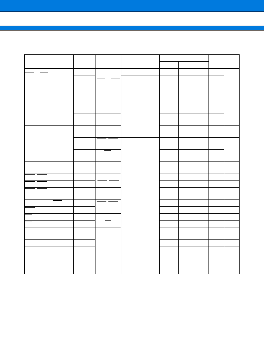
MB91350A Series
90
(4) Normal bus access read/write operation
(V
CC
=
3.0 V to 3.6 V, V
SS
=
DA
VS
=
AV
SS
=
0 V, Ta
=
-
40
∞
C to
+
85
∞
C)
*1 : When the bus timing is delayed by automatic wait insertion or RDY input, add the time (t
CYC
◊
the number of
cycles added for the delay) to this rating.
*2 : The following ratings are for the gear ratio set to
◊
1. For the ratings when the gear ratio is set to between 1/2 to
1/16, substitute 1/2 to 1/16 for n in the following equation.
Calculation expression: 3/(2n)
◊
t
CYC
-
15
*3 : AWRxL : Area Wait Register
Note : t
CYC
indicates the cycle time. See "(2) Clock output timing".
Parameter
Symbol
Pin
Conditions
Value
Unit
Remarks
Min
Max
CS0 to CS3 setup
t
CSLCH
MCLK,
CS0 to CS3
AWRxL*
3
: W02
=
0
3
ns
t
CSDLCH
AWR0L : W02
=
1
-
3
ns
CS0 to CS3 hold
t
CHCSH
3
t
CYC
/2
+
6
ns
Address setup
t
ASCH
MCLK,
A23 to A00
3
ns
t
ASWL
WR0, WR1,
A23 to A00
3
ns
t
ASRL
RD,
A23 to A00
3
ns
Address hold
t
CHAX
MCLK,
A23 to A00
3
t
CYC
/2
+
6
ns
t
WHAX
WR0, WR1,
A23 to A00
3
ns
t
RHAX
RD,
A23 to A00
3
ns
Valid address
Valid data input time
t
AVDV
A23 to A00,
D31 to D16
3 / 2
◊
t
CYC
-
15
ns
*1
*2
WR0, WR1 delay time
t
CHWL
MCLK,
WR0, WR1
6
ns
WR0, WR1 delay time
t
CHWH
6
ns
WR0, WR1 minimum
pulse width
t
WLWH
WR0, WR1
t
CYC
-
5
ns
Data setup
WRx
t
DSWH
WR0, WR1,
D31 to D16
t
CYC
ns
WRx
Data hold time
t
WHDX
3
ns
RD delay time
t
CHRL
MCLK,
RD
6
ns
RD delay time
t
CHRH
6
ns
RD
Valid data input time
t
RLDV
RD,
D31 to D16
t
CYC
-
10
ns
*1
Data setup
RD
Time
t
DSRH
10
ns
RD
Data hold time
t
RHDX
0
ns
RD minimum pulse width
t
RLRH
RD
t
CYC
-
5
ns
AS setup
t
ASLCH
MCLK,
AS
3
ns
AS hold
t
CHASH
3
t
CYC
/2
+
6
ns
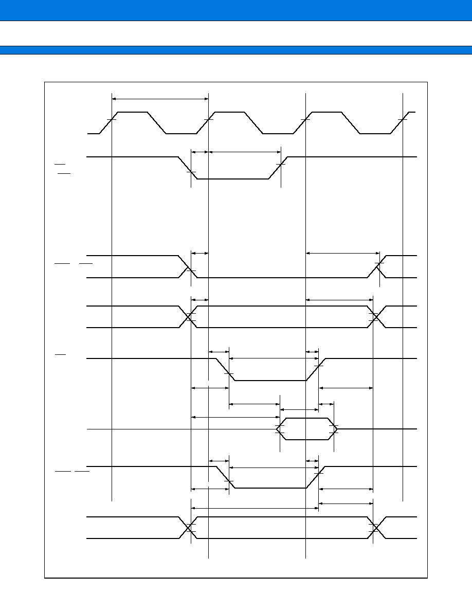
MB91350A Series
91
MCLK
CS0 to CS3
V
OH
V
OH
V
OH
V
OL
V
OL
V
OH
V
OH
V
OL
V
OH
V
OL
V
OL
V
OL
A23 to A00
RD
D31 to D16
WR0, WR1
D31 to D16
V
OH
V
OH
V
OH
V
OH
V
OL
V
OH
V
OL
V
OH
V
OL
V
OH
t
ASCH
t
AVDV
t
RLDV
t
DSRH
t
RHDX
t
WLWH
t
CHWL
t
CHWH
t
CHAX
t
CHRH
t
DSWH
t
WHDX
t
CYC
t
CHCSH
t
CHRL
t
RLRH
t
CSLCH
AS
(LBA)
V
OL
V
OH
t
CHASH
t
ASLCH
BA1
t
ASRL
t
RHAX
t
ASWL
t
WHAX
write
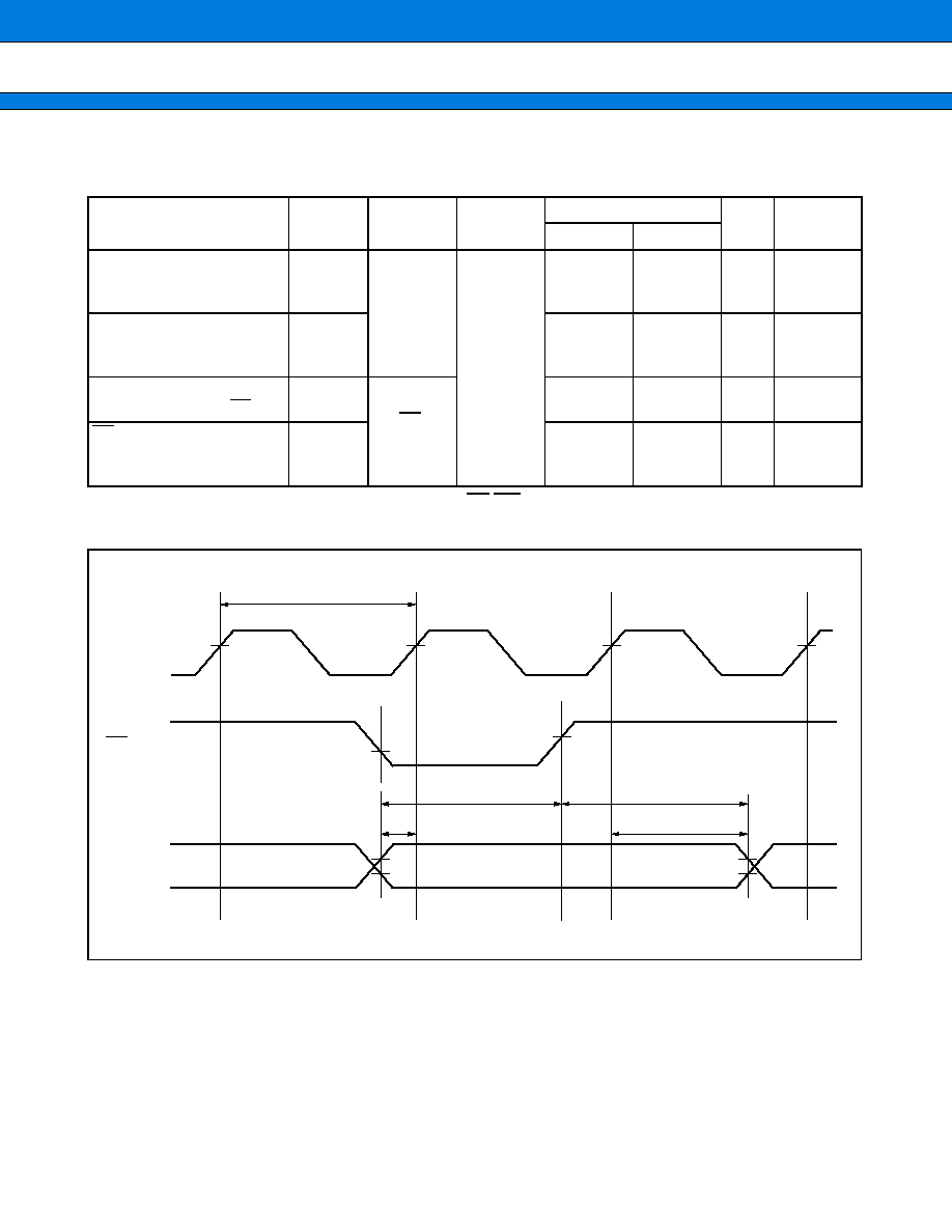
MB91350A Series
92
(5) Multiplex bus access read/write operation
(V
CC
=
3.0 V to 3.6 V, V
SS
=
DA
VS
=
AV
SS
=
0 V, Ta
=
-
40
∞
C to
+
85
∞
C)
Notes :
∑
This rating is not guaranteed when the CS
RD/WR, and setup delay setting by AWR: bit 1 is "0".
∑
Beside This rating, normal bus interface ratings are applicable.
∑
t
CYC
indicates the cycle time. See "(2) Clock output timing".
Parameter
Symbol
Pin
Condi-
tions
Value
Unit
Remarks
Min
Max
AD15 to AD0 Address
AUDI setup time
MCLK
t
ASCH
MCLK,
D31 to D16
3
ns
MCLK
AD15 to AD0 Address
AUDI Hold Time
t
CHAX
3
t
CYC
/2
+
6
ns
AD15 to AD0 Address
AUDI setup time
AS
t
ASASH
AS,
D31 to D16
12
ns
AS
AD15 to AD0 Address
AUDI Hold Time
t
ASHAX
t
CYC
-
3
t
CYC
+
3
ns
MCLK
V
OH
V
OL
D31 to D16
V
OH
V
OH
V
OH
V
OH
V
OL
V
OH
t
ASCH
t
CHAX
t
ASASH
t
ASHAX
t
CYC
AS
V
OL
V
OH
BA1
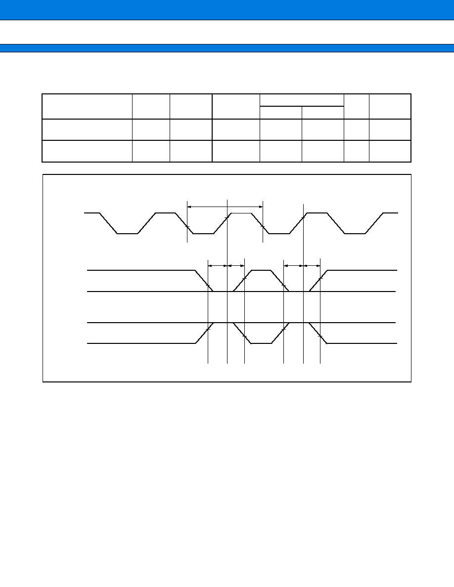
MB91350A Series
93
(6) Ready input timings
(V
CC
=
3.0 V to 3.6 V, V
SS
=
DA
VS
=
AV
SS
=
0 V, Ta
=
-
40
∞
C to
+
85
∞
C)
Parameter
Symbol
Pin
Conditions
Value
Unit
Remarks
Min
Max
RDY setup time
MCLK
t
RDYS
MCLK,
RDY
15
ns
MCLK
RDY hold time
t
RDYH
MCLK,
RDY
0
ns
MCLK
V
OH
V
OH
V
OL
V
OL
V
OL
V
OH
V
OL
V
OH
V
OH
V
OL
V
OH
V
OL
t
RDYH
t
RDYH
RDY
RDY
t
CYC
t
RDYS
t
RDYS
with wait
without wait
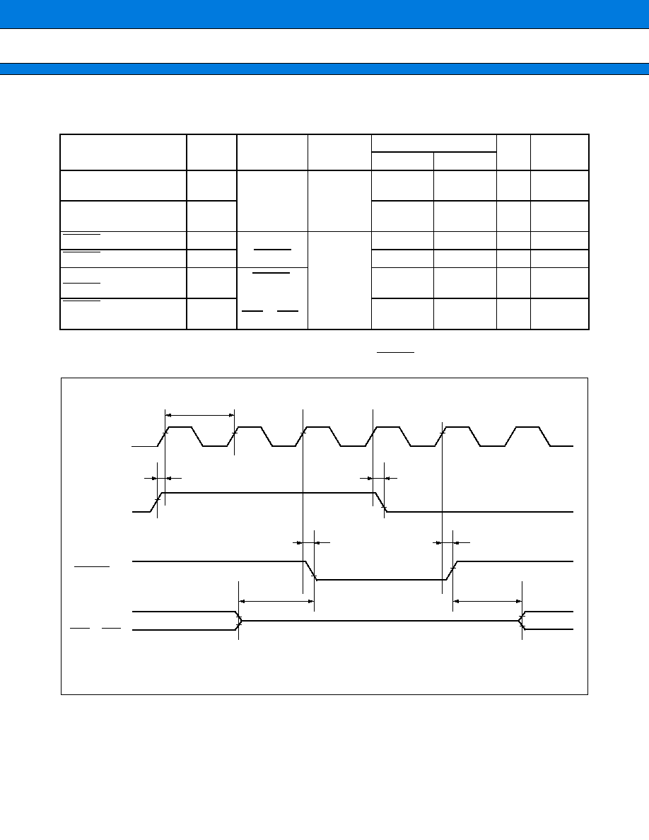
MB91350A Series
94
(7) Hold timing
(V
CC
=
3.0 V to 3.6 V, V
SS
=
DA
VS
=
AV
SS
=
0 V, Ta
=
-
40
∞
C to
+
85
∞
C)
* : These are applied to only the case that SREN bit of area select register (ACR) is set to "1".
Notes :
∑
It takes 1 cycle or more from when BRQ is captured until BGRNT changes.
∑
t
CYC
indicates the cycle time. See "(2) Clock output timing".
Parameter
Symbol
Pin
Conditions
Value
Unit
Remarks
Min
Max
BRQ setup time
MCLK
t
BRQS
MCLK,
BRQ
15
ns
MCLK
BRQ
AUDI Hold Time
t
BRQH
0
ns
BGRNT delay time
t
CHBGL
MCLK,
BGRNT
t
CYC
/2
-
6
t
CYC
/2
+
6
ns
BGRNT delay time
t
CHBGH
t
CYC
/2
-
6
t
CYC
/2
+
6
ns
Pin floating
BGRNT
time
t
XZBGL
BGRNT,
D31 to D16,
A23 to A00,
CS3 to CS0*
t
CYC
-
10
t
CYC
+
10
ns
BGRNT
Pin valid time
t
BGHXV
t
CYC
-
10
t
CYC
+
10
ns
MCLK
V
OH
t
CHBGL
V
OL
V
OH
V
OH
V
OL
V
OH
V
OH
V
OH
t
CHBGH
BRQ
BGRNT
t
CYC
t
BGHXV
t
XZBGL
t
BRQS
t
BRQH
D31 to D16,
A23 to A00,
CS3 to CS0 *
High-Z
* : These are applied to only the case that SREN bit of area select register (ACR) is set to "1".
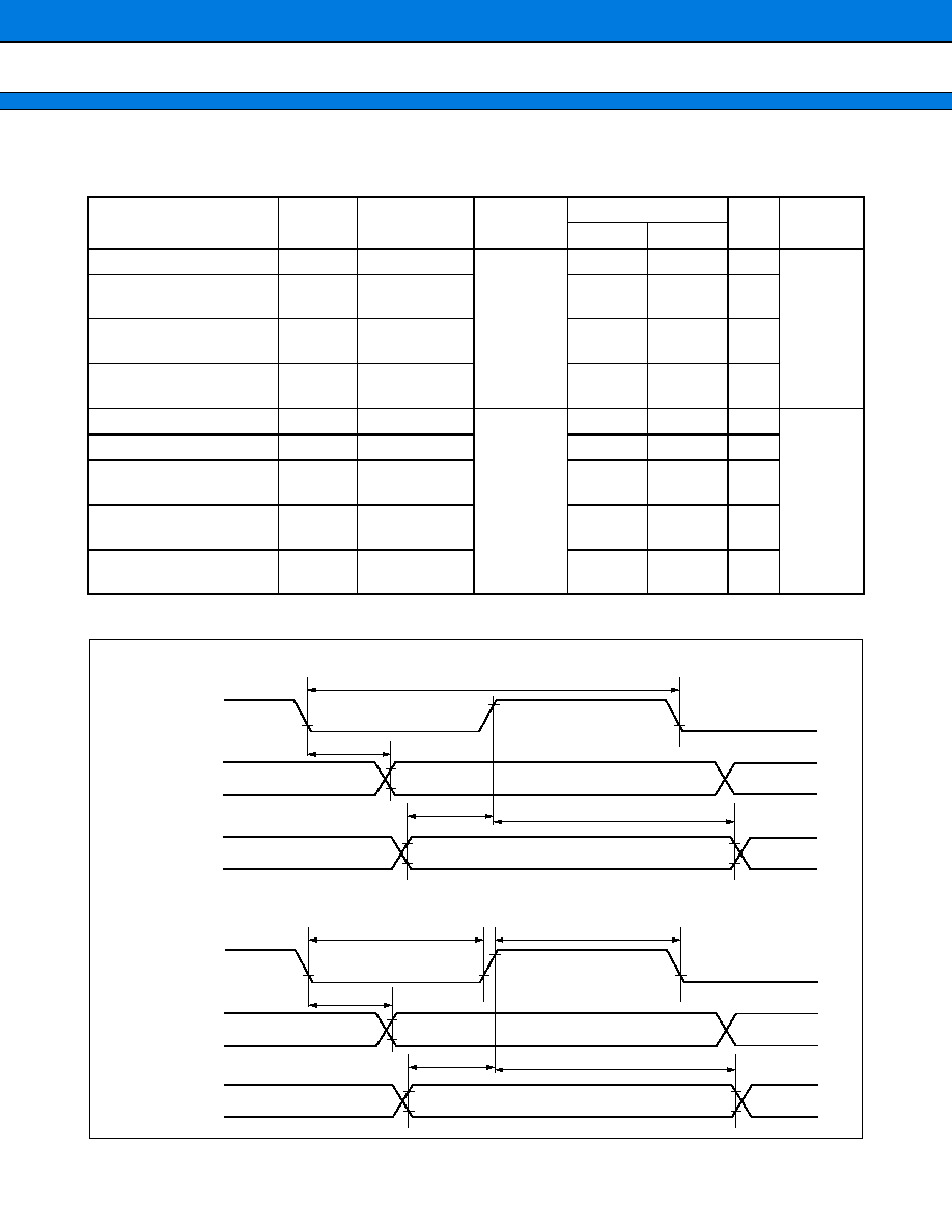
MB91350A Series
95
(8) UART, SIO timing
(V
CC
=
3.0 V to 3.6 V, V
SS
=
DA
VS
=
AV
SS
=
0 V, Ta
=
-
40
∞
C to
+
85
∞
C)
Notes :
∑
Above rating is for CLK synchronous mode.
∑
t
CPP
indicates the peripheral clock cycle time. See "(1) Clock timing".
Parameter
Symbol
Pin
Conditions
Value
Unit
Remarks
Min
Max
Serial clock cycle time
t
SCYC
SCK0 to SCK7
Internal shift
clock
mode
8 t
CPP
ns
SCK
BGRNT delay time
t
SLOV
SCK0 to SCK7,
SO0 to SO7
-
80
+
80
ns
Valid SI
SCK
t
IVSH
SCK0 to SCK7,
SI0 to SI7
100
ns
SCK
valid SIN hold
time
t
SHIX
SCK0 to SCK7,
SI0 to SI7
60
ns
Serial clock H Pulse Width
t
SHSL
SCK0 to SCK7
External
shift clock
mode
4 t
CPP
ns
Serial clock L Pulse Width
t
SLSH
SCK0 to SCK7
4 t
CPP
ns
SCK
SO delay time
t
SLOV
SCK0 to SCK7,
SO0 to SO7
150
ns
Valid SI
SCK
t
IVSH
SCK0 to SCK7,
SI0 to SI7
60
ns
SCK
valid SI hold
time
t
SHIX
SCK0 to SCK7,
SI0 to SI7
60
ns
∑ Internal shift clock mode
∑ External shift clock mode
SCK0 to SCK7
SO0 to SO7
SI0 to SI7
t
SCYC
t
SLOV
t
IVSH
t
SHIX
V
OL
V
OH
V
OL
V
OH
V
OL
V
OH
V
OL
V
OH
V
OL
SCK0 to SCK7
SO0 to SO7
SI0 to SI7
t
SLOV
t
SLSH
t
SHSL
t
IVSH
t
SHIX
V
OH
V
OL
V
OH
V
OL
V
OL
V
OL
V
OH
V
OL
V
OH
V
OL
MB91350A Series
96
(9) Free-run timer clock, PPG timer input timing
(V
CC
=
3.0 V to 3.6 V, V
SS
=
DA
VS
=
AV
SS
=
0 V, Ta
=
-
40
∞
C to
+
85
∞
C)
Note : t
CPP
indicates the peripheral clock cycle time. See "(1) Clock timing".
(10) Trigger input timing
(V
CC
=
3.0 V to 3.6 V, V
SS
=
DA
VS
=
AV
SS
=
0 V, Ta
=
-
40
∞
C to
+
85
∞
C)
Note : t
CPP
indicates the peripheral clock cycle time. See "(1) Clock timing".
Parameter
Symbol
Pin
Conditions
Value
Unit
Remarks
Min
Max
Input pulse width
t
TIWH
t
TIWL
FRCK,
TRG0 to TRG5,
AIN0 to AIN1,
BIN0 to BIN1,
ZIN0 to ZIN1
2 t
CPP
ns
Parameter
Symbol
Pin
Conditions
Value
Unit
Remarks
Min
Max
A/D activation trigger input
time
t
ATGX
ATG
5 t
CPP
ns
input capture
input trigger
t
INP
IN0 to IN3
5 t
CPP
ns
t
TIWH
t
TIWL
ATG,
IN0 to IN3
t
ATGX
, t
INP
MB91350A Series
97
(11)DMA controller timing
∑ For edge detection (block/step transfer mode,burst transfer mode)
(V
CC
=
3.0 V to 3.6 V, V
SS
=
DA
VS
=
AV
SS
=
0 V, Ta
=
-
40
∞
C to
+
85
∞
C)
* : t
CYC
becomes t
CP
when f
CPT
is greater than f
CP
.
∑ For level detection (demand transfer mode)
(V
CC
=
3.0 V to 3.6 V, V
SS
=
DA
VS
=
AV
SS
=
0 V, Ta
=
-
40
∞
C to
+
85
∞
C)
∑ Common operation mode
(V
CC
=
3.0 V to 3.6 V, V
SS
=
DA
VS
=
AV
SS
=
0 V, Ta
=
-
40
∞
C to
+
85
∞
C)
* : AWRxL: Area Wait Register.
Note : t
CYC
indicates the cycle time. See "(2) Clock output timing".
Parameter
Symbol
Pin
Conditions
Value
Unit
Remarks
Min
Max
DREQ Input pulse width
t
DRWL
DREQ 0 to DREQ2
2 t
CYC
*
ns
DREQ Input pulse width
t
DSWH
DSTP 0 to DSTP2
2 t
CYC
*
ns
Parameter
Symbol
Pin
Condi-
tions
Value
Unit Remarks
Min
Max
DREQ setup time
t
DRS
MCLK, DREQ 0 to DREQ2
15
ns
DREQ Hold Time
t
DRH
MCLK, DREQ 0 to DREQ2
0.0
ns
DSTP setup time
t
DSTPS
MCLK, DSTP 0 to DSTP2
15
ns
DSTP Hold Time
t
DSTPH
MCLK,DSTP 0 to DSTP2
0.0
ns
Parameter
Symbol
Pin
Condi-
tions
Value
Unit
Remarks
Min
Max
DACK delay time
t
DALCH
MCLK,
DACK 0 to
DACK2
AWRxL* :
W02
=
0
3
ns
CS timing
6
ns
FR30 compatible
t
DADLCH
AWR0L :
W02
=
1
-
3
ns
CS timing
6
ns
FR30 compatible
t
CHDAH
t
CYC
/2
+
6
ns
CS timing
6
ns
FR30 compatible
DEOP delay time
t
DELCH
MCLK,
DEOP 0 to
DEOP2
AWR0L :
W02
=
0
3
ns
CS timing
6
ns
FR30 compatible
t
DEDLCH
AWRxL* :
W02
=
1
-
3
ns
CS timing
6
ns
FR30 compatible
t
CHDEH
t
CYC
/2
+
6
ns
CS timing
6
ns
FR30 compatible
IORD delay time
t
CHIRL
MCLK,
IORD
6
ns
t
CHIRH
6
ns
IOWR delay time
t
CHIWL
MCLK,
IOWR
6
ns
t
CHIWH
6
ns
IORD minimum pulse width
t
IRLIRH
IORD
12
ns
IOWR minimum pulse width
t
IWLIWH
IOWR
12
ns
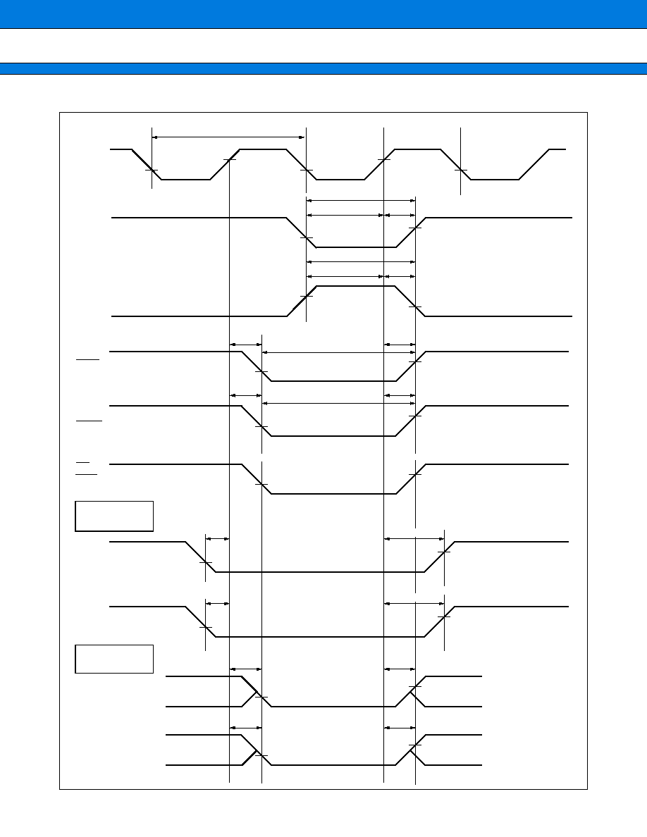
MB91350A Series
98
MCLK
DACK0 to DACK2
DACK0 to DACK2
DREQ0 to DREQ2
DSTP0 to DSTP2
IORD
V
OL
V
OH
V
OL
V
OL
V
OH
V
OL
V
OH
V
OL
V
OH
V
OL
V
OH
V
OL
V
OH
V
OL
V
OH
V
OL
V
OH
V
OL
V
OH
t
DALCH
t
DADLCH
t
CHIRL
t
CHIWL
t
IRLIRH
t
IWLIWH
t
DALCH
t
DADLCH
t
CYC
t
CHIRH
t
CHIWH
t
DRS
t
DRH
t
DSTPS
t
DSTPH
t
DRWL
t
DSWH
t
CHDAH
DEOP0 to DEOP2
V
OL
V
OH
t
DELCH
t
DEDLCH
t
CHDEH
IOWR
RD,
WRn
DEOP0 to DEOP2
V
OL
V
OH
t
DELCH
t
DEDLCH
t
CHDAH
t
CHDEH
Chip select
timing
FR30 compatible
timing
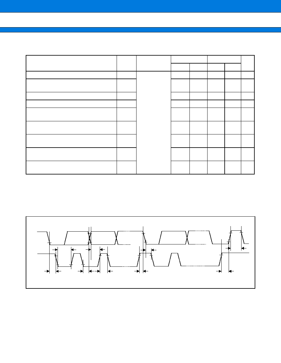
MB91350A Series
99
(12) I
2
C Timing
(V
CC
=
3.0 V to 3.6 V, V
SS
=
DA
VS
=
AV
SS
=
0 V, Ta
=
-
40
∞
C to
+
85
∞
C)
*1 : R,C : Pull-up resistor and load capacitor of the SCL and SDA lines.
*2 : The maximum t
HDDAT
only has to be met if the device does not stretch the "L" width (t
LOW
) of the SCL signal.
*3 : A Fast-mode I
2
C-bus device can be used in a Standard-mode I
2
C-bus system, but the requirement
t
SUDAT
250 ns must then be met.
*4 : For use at over 100 kHz, set the machine clock to at least 6 MHz.
Parameter
Symbol
Condition
Standard-mode
Fast-mode*
4
Unit
Min
Max
Min
Max
SCL clock frequency*
4
f
SCL
R
=
1.0 k
,
C
=
50 pF*
1
0
100
0
400
kHz
Hold time (repeated) START condition
SDA
SCL
t
HDSTA
4.0
0.6
µ
s
"L" width of the SCL clock
t
LOW
4.7
1.3
µ
s
"H" width of the SCL clock
t
HIGH
4.0
0.6
µ
s
Set-up time for a repeated START condition
SCL
SDA
t
SUSTA
4.7
0.6
µ
s
Data hold time
SCL
SDA
t
HDDAT
0
3.45*
2
0
0.9*
3
µ
s
Data set-up time
SDA
SCL
t
SUDAT
250
100
ns
Set-up time for STOP condition
SCL
SDA
t
SUSTO
4.0
0.6
µ
s
Bus free time between a STOP and START
condition
t
BUS
4.7
1.3
µ
s
SDA
SCL
t
LOW
t
SUDAT
t
HDSTA
t
BUS
t
HDSTA
t
HDDAT
t
HIGH
t
SUSTA
t
SUSTO
MB91350A Series
100
5.
Electrical Characteristics for the A/D Converter
(V
CC
=
AV
CC
=
3.0 V to 3.6 V, V
SS
=
DA
VS
=
AV
SS
=
0 V, AVRH
=
3.0 V to 3.6 V, Ta
=
-
40
∞
C to
+
85
∞
C)
*1: Measured in the CPU sleep state
*2: When the peripheral resource clock frequency is 25.0 MHz, set the Conversion Time Setting Register (ADCT)
to a value equal to or greater than 5334
H
.
Set each bit as follow :
Sampling time
: SAMP3 to SAMP0
5
H
Conversion time a : CV03 to CV0
3
H
Conversion time b : CV13 to CV0
3
H
Conversion time c : CV23 to CV0
4
H
Parameter
Symbol
Pin
Value
Unit
Remarks
Min
Typ
Max
Resolution
10
bit
Total error*
1
-
5.0
+
5.0
LSB
AVcc
=
3.3 V,
AVRH
=
3.3 V
Nonlinear error*
1
-
3.5
+
3.5
LSB
Differential linear error*
1
-
2.5
+
2.5
LSB
Zero transition voltage*
1
AN11
to AN0
AVRL
-
2.0
AVRL
+
1.0
AVRL
+
6.0
LSB
Full-transition voltage*
1
AN11
to AN0
AVRH
-
5.5
AVRH
+
1.5
AVRH
+
3.0
LSB
Conversion time
1.48*
2
300
µ
s
Analog power supply current
(analog + digital)
I
A
AV
CC
8
mA
I
AH
5
µ
A
At stop
Reference power supply
current
(between AVRH and AVRL)
I
R
AVRH
470
µ
A
AVRH
=
3.0 V,
AVRL
=
0.0 V
I
RH
10
µ
A
At stop
Analog input capacitance
AN11
to AN0
40
pF
Interchannel disparity
AN11
to AN0
4
LSB
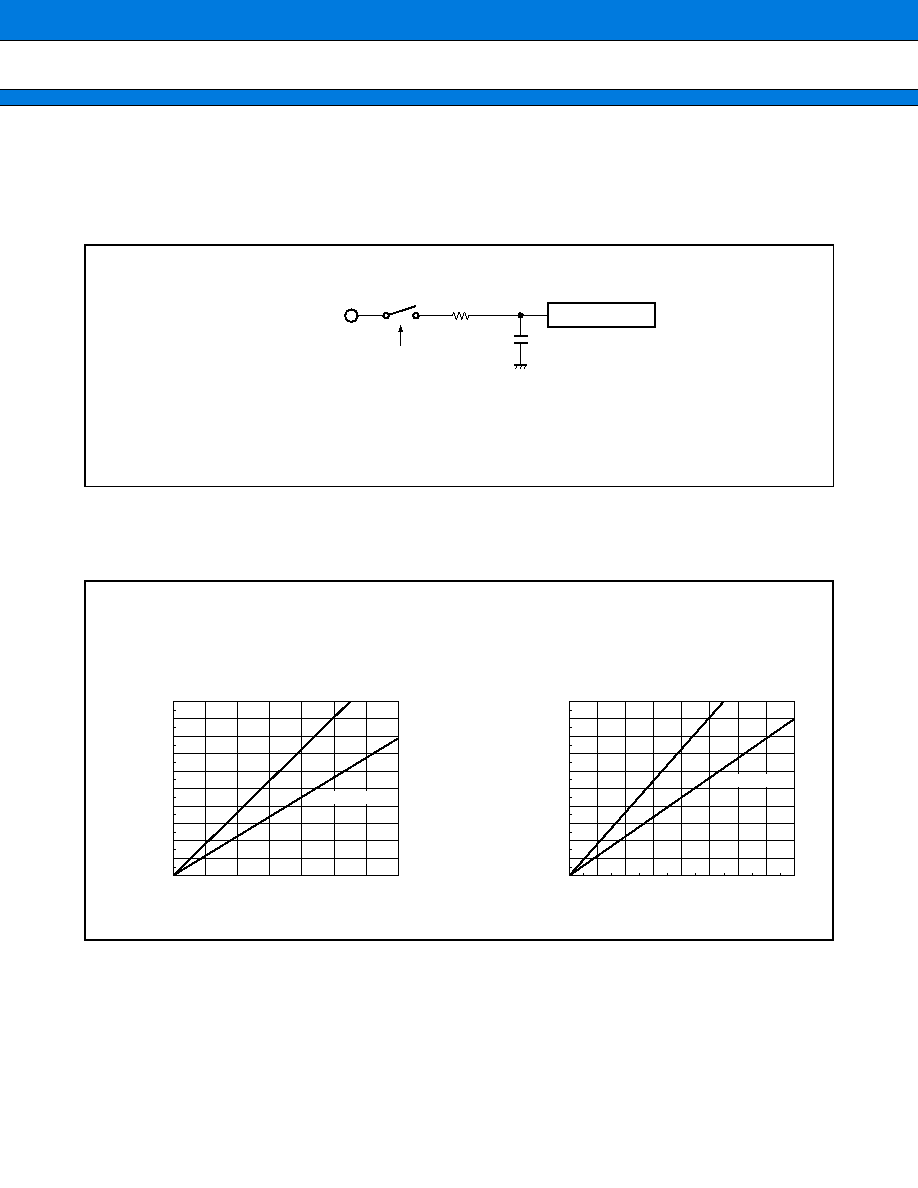
MB91350A Series
101
∑
About the external impedance of the analog input and its sampling time
∑ A/D converter with sample and hold circuit. If the external impedance is too high to keep sufficient sampling
time, the analog voltage charged to the internal sample and hold capacitor is insufficient, adversely affecting
A/D conversion precision.
∑ To satisfy the A/D conversion precision standard, consider the relationship between the external impedance
and minimum sampling time and either adjust the resistor value and operating frequency or decrease the
external impedance so that the sampling time is longer than the minimum value.
∑ If the sampling time cannot be sufficient, connect a capacitor of about 0.1
µ
F to the analog input pin.
∑
About errors
As |AVRH-AV
SS
| becomes smaller, values of relative errors grow larger.
R
C
Analog input
Comparator
∑
Analog input circuit model
During Sampling : ON
Note : The values are reference values.
R
C
MB91355A
0.18 k
(Max)
63.0 pF (Max)
MB91F355A
0.18 k
(Max)
39.0 pF (Max)
MB91F356B
0.18 k
(Max)
39.0 pF (Max)
100
90
80
70
60
50
40
30
20
10
0
0
5
10
15
20
25
30
35
MB91F355A/MB91F356B
MB91355A
20
18
16
14
12
10
8
6
4
2
0
0
1
2
3
4
5
6
8
7
MB91F355A/MB91F356B
MB91355A
(External impedance
=
0 k
to 100 k
)
External impedance [k
]
Minimum sampling time [
µ
s]
(External impedance
=
0 k
to 20 k
)
External impedance [k
]
Minimum sampling time [
µ
s]
∑
The relationship between the external impedance and minimum sampling time
MB91350A Series
102
Definition of A/D Converter Terms
∑ Resolution
Analog variation that is recognized by an A/D converter.
∑ Linearity error
Zero transition point ( "0000000000" - "0000000001") and full-scale transition point
Difference between the line connected ("1111111110" - "1111111111") and actual conversion characteristics.
∑ Differential linear error
Deviation of input voltage, which is required for changing output code by 1 LSB, from an ideal value.
V
NT
: A voltage at which digital output transitions from (N - 1) to N.
Linear error in digital output N
=
V
NT
-
{1 LSB'
◊
(N
-
1)
+
{V
OT
}
1 LSB'
[LSB]
Differential linear error in digital output N
=
V
(N
+
1) T
-
V
NT
1 LSB'
-
1 [LSB]
1 LSB
=
V
FST
-
V
OT
1022
[V]
V
FST
: A voltage at which digital output transitions from (3FE)
H
to (3FF)
H
.
3FF
H
3FE
H
3FD
H
004
H
003
H
002
H
001
H
AV
SS
AVRH
{1 LSB' (N
-
1)
+
V
OT
}
N
-
1
AV
SS
AVRH
N
-
2
N
N
+
1
Linearity error
Differential linear error
Digital output
Digital output
Actual conversion
characteristic
V
FST
(measure-
ment value)
V
NT
(measurement value)
Actual conversion
characteristic
Ideal characteristics
V
OT
(measurement value)
Analog input
Analog input
Ideal characteristics
Actual conversion
characteristic
V
(N+1)T
(measurement
value)
V
NT
(measurement value)
Actual conversion characteristic
V
OT
: A voltage at which digital output transitions from (000)
H
to (001)
H
.
MB91350A Series
103
∑ Total error
This error indicates the difference between actual and ideal values, including the zero transition error/full-scale
transition error/linearity error.
3FF
H
3FE
H
3FD
H
004
H
003
H
002
H
001
H
AV
SS
AVRH
1.5 LSB'
0.5 LSB'
{1 LSB' (N
-
1)
+
0.5 LSB'}
Total error
Digital output
Actual conversion
characteristic
V
NT
(measurement
value)
Analog input
Total error of digital output N
=
V
NT
-
{1 LSB'
◊
(N
-
1)
◊
{0.5 LSB'}
1 LSB'
V
OT
'(Ideal value)
=
AV
SS
+
{0.5 LSB' [V]
V
FST
'(Ideal value)
=
AVRH
-
1.5 LSB' [V]
V
NT
: A voltage at which digital output transitions from (N + 1) to (N).
1LS' (Ideal value) 1
=
AVRH
-
AV
SS
1024
[V]
Actual
characteristics
Ideal characteristics
MB91350A Series
104
6.
Electrical Characteristics for the D/A Converter
(V
CC
=
DA
VC
=
3.0 V
=
3.6 V, V
SS
=
DA
VS
=
0 V, Ta
=
-
40
∞
C to
+
85
∞
C)
* : This D/A converter varies in current consumption depending on each input digital code.
This rating indicates the current consumption when the digital code that maximizes current consumption is input.
Parameter
Symbol
Pin
Value
Unit
Remarks
Min
Typ
Max
Resolution
8
bit
Nonlinear error
-
2.0
+
2.0
LSB
When the output is unloaded
Differential linear error
-
1.0
+
1.0
LSB
When the output is unloaded
Convertion speed
0.6
µ
s
When load capacitance (C
L
) = 20 pF
3.0
µ
s
When load capacitance (C
L
) = 100 pF
Output high impedance
DA0 to
DA2
2.0
2.9
3.8
k
Analog current
DA
VC
40
µ
A
10
µ
s conversion when the output is
unloaded
I
ADA
460*
µ
A
Input digital code
When fixed at 7A
H
or 85
H
I
ADAH
0.1
µ
A
At power-down
MB91350A Series
105
FLASH MEMORY WRITE/ERASE CHARACTERISTICS
*: This value comes from the technology qualification (using Arrhenius equation to translate high temperature
measurements into normalized value at
+
85
∞
C).
Parameter
Condition
Value
Unit
Remarks
Min
Typ
Max
Sector erase time
Ta
=
+
25
∞
C,
V
CC
=
3.3 V
1
15
s
Excludes 00
H
programming
prior erasure.
Chip erase time
8
s
Excludes 00
H
programming
prior erasure.
Half word (16-bit
width) writing time
16
3,600
µ
s
Excludes system-level
overhead.
Write/erase cycle
10,000
cycle
Flash data retention
time
Average
Ta
=
+
85
∞
C
20
year
*
MB91350A Series
106
EXAMPLE CHARACTERISTICS
(Continued)
(1) "H" level output voltage
(2) "L" level output voltage
(3) "L" level output voltage (Nch open-drain)
(4) Input leak current
(5) Pull-up resistance
4
3
2
1
0
2.7
3.0
3.3
3.6
3.9
V
OH
[V]
V
CC
[V]
V
OH
- V
CC
Ta = +25
∞
C
V
OL1
[mV]
V
CC
[V]
2.7
3.0
3.3
3.6
3.9
0
100
200
300
400
500
V
OL1
- V
CC
Ta = +25
∞
C
V
OL2
[mV]
V
CC
[V]
2.7
3.0
3.3
3.6
3.9
0
100
200
300
400
500
V
OL2
- V
CC
Ta = +25
∞
C
2.7
3.0
3.3
3.6
3.9
-
6
-
4
-
2
0
2
4
6
I
LI
[
µ
A]
V
CC
[V]
I
LI
- V
CC
Ta = +25
∞
C
2.7
3.0
3.3
3.6
3.9
V
CC
[V]
R
UP
[k
]
200
160
120
80
40
0
R
UP
- V
CC
Ta = +25
∞
C
MB91350A Series
107
(Continued)
(6) Power supply current
(7) Power supply current
(8) Power supply current at sleep
(9) Power supply current at sleep
(10) Power supply current at stop
(11) Sub RUN power supply current
(12) Sub sleep power supply current
(13) Watch mode power supply current
I
CC
[mA]
V
CC
[V]
2.7
3.0
3.3
3.6
3.9
300
250
200
150
100
50
0
I
CC
- V
CC
Ta = +25
∞
C, f
CP
= 50 MHz,
f
CCP
= f
CPT
= 25 MHz
1
10
100
300
250
200
150
100
50
0
I
CC
[mA]
f
C
[MHz]
I
CC
- f
C
Ta = +25
∞
C, V
CC
= 3.3 V,
f
CP
= 4
◊
f
C (multiplied by 4)
I
CCS
[mA]
V
CC
[V]
2.7
3.0
3.3
3.6
3.9
300
250
200
150
100
50
0
I
CCS
- V
CC
Ta = +25
∞
C, f
CP
= 50 MHz,
f
CCP
= f
CPT
= 25 MHz
1
10
100
300
250
200
150
100
50
0
I
CCS
[mA]
f
C
[MHz]
I
CCS
- f
C
Ta = +25
∞
C, V
CC
= 3.3 V,
f
CP
= 4
◊
f
C (multiplied by 4)
V
CC
[V]
2.7
3.0
3.3
3.6
3.9
I
CCH
[
µ
A]
-
20
0
20
40
60
80
100
I
CCH
- V
CC
Ta = +25
∞
C
V
CC
[V]
2.7
3.0
3.3
3.6
3.9
I
CCL
[
µ
A]
0
100
200
300
400
500
I
CCL
- V
CC
Ta = +25
∞
C, f
CP
= 32 kHz,
f
CCP
= f
CPT
= 32 kHz
500
400
300
200
100
0
2.7
3.0
3.3
3.6
3.9
I
CCLS
[
µ
A]
V
CC
[V]
I
CCLS
- V
CC
Ta = +25
∞
C, f
CP
= 32 kHz,
f
CCP
= f
CPT
= 32 kHz
V
CC
[V]
I
CCT
[
µ
A]
100
80
60
40
20
0
-
20
2.7
3.0
3.3
3.6
3.9
I
CCT
- V
CC
Ta = +25
∞
C, f
CP
= 32 kHz,
f
CCP
= f
CPT
= 32 kHz
MB91350A Series
108
(Continued)
(14) A/D converter power supply current
(15) A/D converter reference power supply voltage
(16) A/D converter power supply current at stop
(17) A/D converter reference power supply current at stop
(18) D/A converter power supply current
< per 1 channel >
(19) D/A converter power supply current at power down
10
8
6
4
2
0
2.7
3.0
3.3
3.6
3.9
I
A
[mA]
V
CC
[V]
I
A
- V
CC
Ta = +25
∞
C
1000
800
600
400
200
0
2.7
3.0
3.3
3.6
3.9
I
R
[
µ
A]
V
CC
[V]
I
R
- V
CC
Ta = +25
∞
C
20
10
0
2.7
3.0
3.3
3.6
3.9
V
CC
[V]
I
AH
[
µ
A]
-
10
I
AH
- V
CC
Ta = +25
∞
C
20
10
0
2.7
3.0
3.3
3.6
3.9
V
CC
[V]
I
RH
[
µ
A]
-
10
I
RH
- V
CC
Ta = +25
∞
C
500
400
300
200
100
0
2.7
3.0
3.3
3.6
3.9
I
AD
A
[
µ
A]
V
CC
[V]
I
ADA
- V
CC
Ta = +25
∞
C
20
10
0
2.7
3.0
3.3
3.6
3.9
V
CC
[V]
I
AD
AH
[
µ
A]
-
10
I
ADAH
- V
CC
Ta = +25
∞
C
MB91350A Series
109
ORDERING INFORMATION
Part number
Package
Remarks
MB91F355APMT-002
176-pin plastic LQFP
(FPT-176P-M02)
Lead-free Package
MB91F356BPMT
176-pin plastic LQFP
(FPT-176P-M02)
Lead-free Package
MB91355APMT
176-pin plastic LQFP
(FPT-176P-M02)
Lead-free Package
MB91354APMT
176-pin plastic LQFP
(FPT-176P-M02)
Lead-free Package
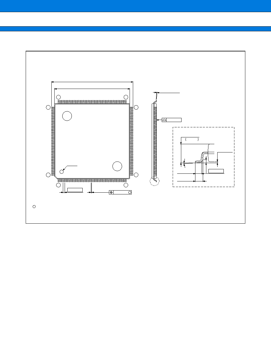
MB91350A Series
110
PACKAGE DIMENSION
176-pin plastic LQFP
(FPT-176P-M02)
Note 1) * : Values do not include resin protrusion.
Resin protrusion is
+
0.25 (.010) Max (each side) .
Note 2) Pins width and pins thickness include plating thickness.
Note 3) Pins width do not include tie bar cutting remainder.
Dimensions in mm (inches).
Note: The values in parentheses are reference values.
C
2003 FUJITSU LIMITED F176006S-c-4-6
Details of "A" part
0∞~8∞
0.50±0.20
(.020±.008)
0.60±0.15
(.024±.006)
0.25(.010)
(Stand off)
(.004±.004)
0.10±0.10
1.50
+0.20
≠0.10
+.008
≠.004
.059
(Mounting height)
0.08(.003)
(.006±.002)
0.145±0.055
"A"
INDEX
1
LEAD No.
44
45
88
89
132
133
176
0.50(.020)
0.22±0.05
(.009±.002)
M
0.08(.003)
24.00±0.10(.945±.004)SQ
26.00±0.20(1.024±.008)SQ
*

MB91350A Series
FUJITSU LIMITED
All Rights Reserved.
The contents of this document are subject to change without notice.
Customers are advised to consult with FUJITSU sales
representatives before ordering.
The information, such as descriptions of function and application
circuit examples, in this document are presented solely for the
purpose of reference to show examples of operations and uses of
Fujitsu semiconductor device; Fujitsu does not warrant proper
operation of the device with respect to use based on such
information. When you develop equipment incorporating the
device based on such information, you must assume any
responsibility arising out of such use of the information. Fujitsu
assumes no liability for any damages whatsoever arising out of
the use of the information.
Any information in this document, including descriptions of
function and schematic diagrams, shall not be construed as license
of the use or exercise of any intellectual property right, such as
patent right or copyright, or any other right of Fujitsu or any third
party or does Fujitsu warrant non-infringement of any third-party's
intellectual property right or other right by using such information.
Fujitsu assumes no liability for any infringement of the intellectual
property rights or other rights of third parties which would result
from the use of information contained herein.
The products described in this document are designed, developed
and manufactured as contemplated for general use, including
without limitation, ordinary industrial use, general office use,
personal use, and household use, but are not designed, developed
and manufactured as contemplated (1) for use accompanying fatal
risks or dangers that, unless extremely high safety is secured, could
have a serious effect to the public, and could lead directly to death,
personal injury, severe physical damage or other loss (i.e., nuclear
reaction control in nuclear facility, aircraft flight control, air traffic
control, mass transport control, medical life support system, missile
launch control in weapon system), or (2) for use requiring
extremely high reliability (i.e., submersible repeater and artificial
satellite).
Please note that Fujitsu will not be liable against you and/or any
third party for any claims or damages arising in connection with
above-mentioned uses of the products.
Any semiconductor devices have an inherent chance of failure. You
must protect against injury, damage or loss from such failures by
incorporating safety design measures into your facility and
equipment such as redundancy, fire protection, and prevention of
over-current levels and other abnormal operating conditions.
If any products described in this document represent goods or
technologies subject to certain restrictions on export under the
Foreign Exchange and Foreign Trade Law of Japan, the prior
authorization by Japanese government will be required for export
of those products from Japan.
F0505
©
2005 FUJITSU LIMITED Printed in Japan