 | –≠–ª–µ–∫—Ç—Ä–æ–Ω–Ω—ã–π –∫–æ–º–ø–æ–Ω–µ–Ω—Ç: MB91V301 | –°–∫–∞—á–∞—Ç—å:  PDF PDF  ZIP ZIP |
DS07-16502-1E
FUJITSU SEMICONDUCTOR
DATA SHEET
32-Bit Proprietary Microcontroller
CMOS
FR65E Series
MB91301/MB91V301
s
DESCRIPTION
The MB91301/MB91V301 are a line of microcontrollers based on a 32-bit RISC CPU core (FR family), incorpo-
rating a variety of I/O resources and a bus control mechanism for embedded control that requires the processing
of a high-performance, fast CPU as well as an SDRAM interface that can connect SDRAM directly to the chip.
The large address space supported by the 32-bit CPU addressing means that operation is primarily based on
external bus access although a large internal RAM area is included for high-speed execution of CPU instructions.
The MB91301 and MB91V301 are FR65E series products based on the FR30/40 series CPU with enhanced bus
access for higher speed operation. The device specifications include a D/A converter to facilitate motor control
and are ideal for use in DVD players that support fly-by transfer.
s
FEATURES
1.
FR CPU
∑ 32-bit RISC, load/store architecture, 5-stage pipeline
∑ 68 MHz internal operating frequency (Max) [external (Max) 68 MHz] (when using PLL with base frequency
(Max) = 17 MHz)
∑ General purpose registers : 32 bits
◊
16
∑ 16-bit fixed length instructions (basic instructions), 1 instruction per cycle
(Continued)
s
PACKAGE
144-pin, Plastic LQFP
179-pin, Ceramic PGA
(FPT-144P-M12)
(PGA-179C-A03)

MB91301/MB91V301
2
∑ Instruction set optimized for embedded applications: Memory-to-memory transfer, bit manipulation, barrel shift
etc.
∑ Instructions adapted for high-level languages: Function entry/exit instructions, multiple-register load/store
instructions
∑ Easier assembler coding: Register interlock function
∑ Branch instructions with delay slots : Reduced overhead time in branch executions
∑ Built-in multiplier with instruction-level support
Signed 32-bit multiplication : 5 cycles
Signed 16-bit multiplication : 3 cycles
∑ Interrupt (PC, PS save) : 6 cycles, 16 priority levels
2.
Bus interface
∑ Operating frequency : Max 68 MHz (when using SDRAM)
∑ Full 24-bit address output (16 MB memory space)
∑ 8-bit, 16-bit or 32-bit data input/output
∑ Built-in pre-fetch buffer
∑ Unused data and address pins can be used as general-purpose input/output ports.
∑ Eight fully independent chip select outputs, can be set in minimum 64 KB units.
∑ Supports the following memory interfaces
Asynchronous SRAM, asynchronous ROM/Flash
Page mode ROM/Flash ROM (selectable page size
=
1, 2, 4, or 8)
Burst mode ROM/Flash ROM (MBM29BL160D/161D/162D)
∑ SDRAM (FCRAM Type, CAS Latency 1 to 8, 2/4 bank products.)
∑ Address/Data multiplex bus (only 8/16-bit width)
∑ Basic bus cycle : 2 cycles
∑ Automatic wait cycle generation function can insert wait cycles, independently programmable for each memory
area.
∑ RDY input for external wait cycles
∑ Endian setting of byte ordering (Big/Little)
CS0 area only for big endian
∑ Prohibition setting of write (only for Read)
∑ Permission/prohibition setting of fetch into built-in cache
∑ Permission/prohibition setting of prefetch function
∑ DMA supports fly-by transfer with independent I/O wait control
∑ External bus arbitration can be used using BRQ and BGRNT.
3.
Built-in memory
∑ 4 KB data RAM
∑ Built-in 8 KB Data RAM and 8 KB instruction, DATA sharing RAM in EVA chip.
4.
Instruction cache (MB91V301 only)
∑ Size : 4 KB
∑ 2-way set associative
∑ 128 blocks/way, 4 entries/block
∑ Lock function enables program code to be made cache-resident
∑ Areas not used for instruction cache can be used as instruction RAM
(Continued)

MB91301/MB91V301
3
(Continued)
5.
DMAC (DMA Controller)
∑ 5-channel (2-channel external-to-external)
∑ 3 transfer triggers : External pin, internal peripheral, software
∑ Capable of selecting an internal peripheral as a transfer source freely for each channel
∑ Addressing using 32-bit full addressing mode (increment, decrement, fixed)
∑ Transfer modes : Demand transfer, burst transfer, step transfer, or block transfer
∑ Supports fly-by transfer (between external I/O and memory)
∑ Selectable transfer data size : 8, 16, or 32-bit
6.
Bit search module
∑ Searches words from MSB for position of first 1/0 bit value change
7.
Reload Timers
∑ 16-bit timer : 3 channels
∑ Internal clock : 2 clock cycle resolution, divide by 2/8/32 selective
8.
UART
∑ Full duplex, double buffer UART
∑ Independent 3 channels
∑ Data length : 7 bits to 9 bits (without parity) , 6 bits to 8 bits (with parity)
∑ Asynchronous (start-stop synchronized) or CLK-synchronous communications selectable
Multi-processor mode
∑ Built-in 16-bit timer (U-TIMER) as a baud rate generator to generate arbitrary baud rates
∑ External clock can be used as transfer clock
∑ Variety of error detection functions (parity, frame, overrun)
9.
Interrupt controller
∑ External interrupt input : 1 non-maskable interrupt pin and 8 normal interrupt pins (INT0 to INT7)
∑ Internal interrupt resources : UART, DMAC, A/D, UTIMER, delay interrupt
∑ Programmable priorities (16 levels) for all interrupts except the non-maskable interrupt
10. A/D converter
∑ 10-bit resolution, 4 channels
∑ Successive approximation type, conversion time : 4.1
µ
s at 34 MHz
∑ Built-in sample and hold circuit
∑ Conversion modes : Single conversion mode, scan conversion mode and repeat conversion mode selectable
∑ Conversion triggers : Software, external trigger and built-in timer selectable
11. Other interval timers
∑ 16-bit timer : 3 channels (U-TIMER)
∑ PPG timer : 4 channels
∑ Watchdog timer : 1 channel
12. Other features
∑ Reset resources : watchdog timer/software reset/external reset (INIT pin)
∑ Power-saving modes : Stop mode, sleep mode
∑ Clock control
Gear function : Allows arbitrary different operating clock frequencies to be set for the CPU and peripherals.
You can select one of the 16 gear clock factors of 1/1 to 1/16. PLL multiplication can also be selected. Note,
however, that peripherals operate at a maximum of 34 MHz.
∑ Packages : MB91301 FPT-144P-M12, MB91V301 PGA-179C-A03
∑ CMOS technology : 0.25
µ
m
∑ Power supply (analog power supply): 3.3 V
±
0.3 V (internal regulator used)
MB91301/MB91V301
4
s
PRODUCT LINEUP
MB91301
MB91V301
Type
External ROM version
(for volume production)
Evaluation version
(For evaluation and development)
RAM
4 KB (only for data)
16 KB (data 8 KB
+
8 KB)
DSU
DSU4
Package
LQFP-144 (0.4 mm pitch)
PGA-179
Other
Currently in production
Currently available
MB91301/MB91V301
5
s
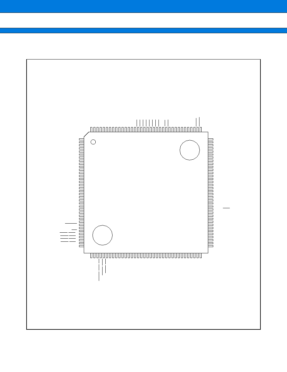
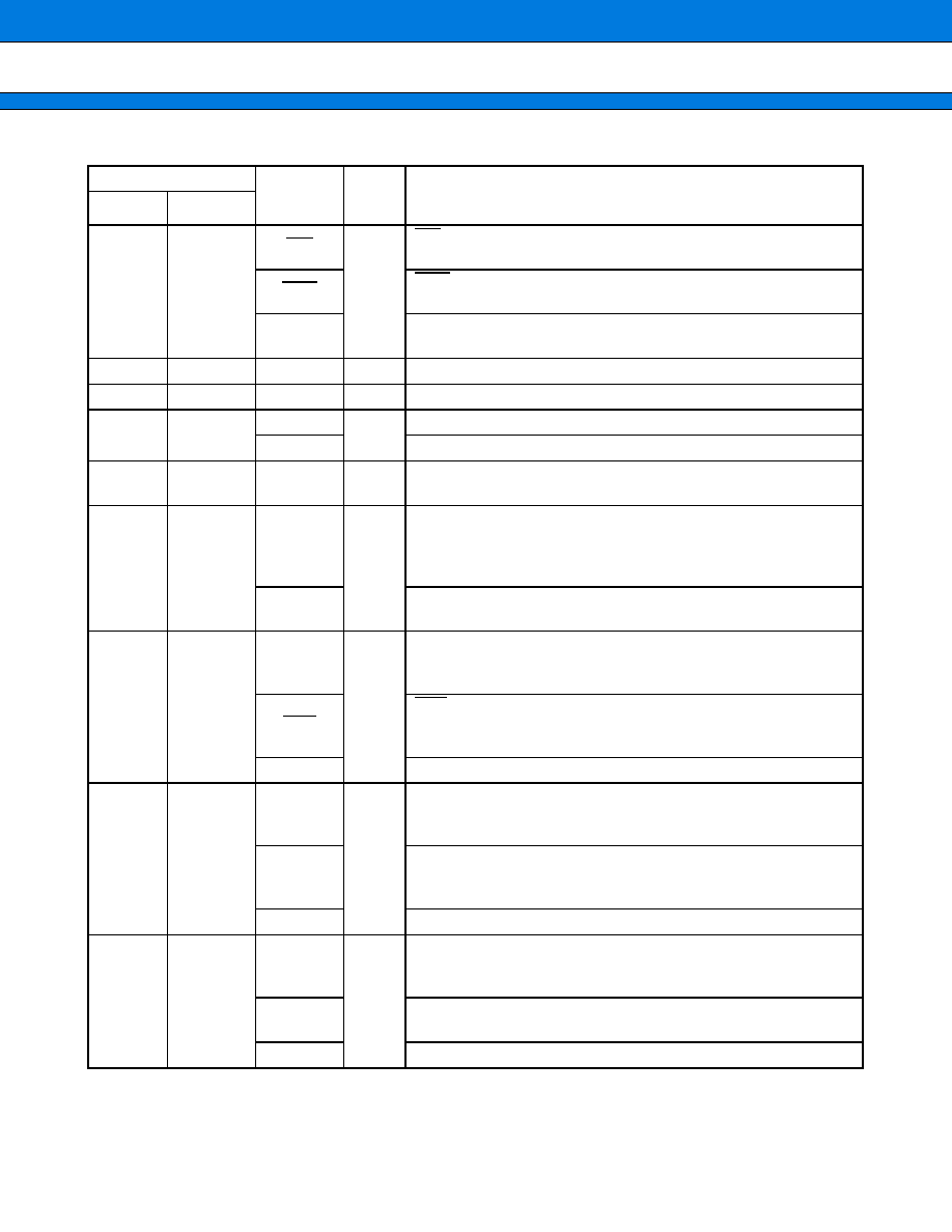
PIN ASSIGNMENTS
∑ MB91301
(TOP VIEW)
(FPT-144P-M12)
1
2
3
4
5
6
7
8
9
10
11
12
13
14
15
16
17
18
19
20
21
22
23
24
25
26
27
28
29
30
31
32
33
34
35
36
37
38
39
40
41
42
43
44
45
46
47
48
49
50
51
52
53
54
55
56
57
58
59
60
61
62
63
64
65
66
67
68
69
70
71
72
108
107
106
105
104
103
102
101
100
99
98
97
96
95
94
93
92
91
90
89
88
87
86
85
84
83
82
81
80
79
78
77
76
75
74
73
144
143
142
141
140
139
138
137
136
135
134
133
132
131
130
129
128
127
126
125
124
123
122
121
120
119
118
117
116
115
114
113
112
111
110
109
P13/D11
P14/D12
P15/D13
P16/D14
P17/D15
V
SS
V
CC
P20/D16
P21/D17
P22/D18
P23/D19
P24/D20
P25/D21
P26/D22
P27/D23
V
SS
V
CC
D24
D25
D26
D27
D28
D29
D30
D31
V
SS
V
CC
P80/RDY
P81/BGRNT
P82/BRQ
RD
DQMUU/WR0(UUB)
P85/DQMUL/WR1(ULB)
P86/DQMLU/WR2(LUB)
P87/DQMLL/WR3(LLB)
P90/SYSCLK
D10/P12
D09/P11
D08/P10
V
CC
V
SS
D07/P07
D06/P06
D05/P05
D04/P04
D03/P03
D02/P02
D01/P01
D00/P00
V
CC
V
SS
CS7/PA7
CS6/PA6
CS5/PPG2/PA5
CS4/TRG2/PA4
CS3/PA3
CS2/PA2
CS1/PA1
CS0/PA0
V
CC
NMI
INIT
MD2
MD1
MD0
V
CC
V
SS
X1
X0
V
CC
IORD/PB7
IOWR/PB6
DEOP1/PPG1/PB5
DACK1/TRG1/PB4
DREQ1/PB3
DEOP0/PB2
DACK0/PB1
DREQ0/PB0
C
V
SS
TIN2/TRG3/PH2
TIN1/PPG3/PH1
TIN0/PH0
TRG0/PJ7
PPG0/PJ6
SCK1/PJ5
SOT1/PJ4
SIN1/PJ3
SCK0/PJ2
SOT0/PJ1
SIN0/PJ0
V
CC
INT7/SCK2/PG7
INT6/SOT2/PG6
INT5/SIN2/PG5
INT4/ATG/PG4
INT3/PG3
INT2/PG2
INT1/PG1
INT0/PG0
AV
SS
/AVRL
AN0
AN1
AN2
AN3
AVR
AVRH
AV
CC
P91/MCLKE
P92/MCLK
P93
P94/SRAS/LBA/AS
P95/SCAS/BAA
P96/SWE/WR
V
SS
V
CC
A00
A01
A02
A03
A04
A05
A06
A07
V
SS
V
CC
A08
A09
A10
A11
A12
A13
A14
A15
V
SS
P60/A16
P61/A17
P62/A18
P63/A19
P64/A20
P65/A21
P66/A22
P67/A23
V
CC
MB91301
MB91301/MB91V301
6
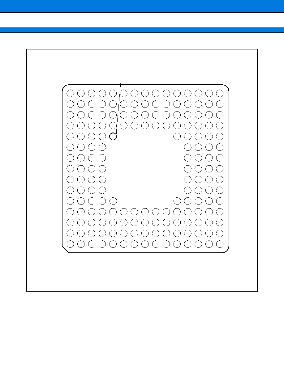
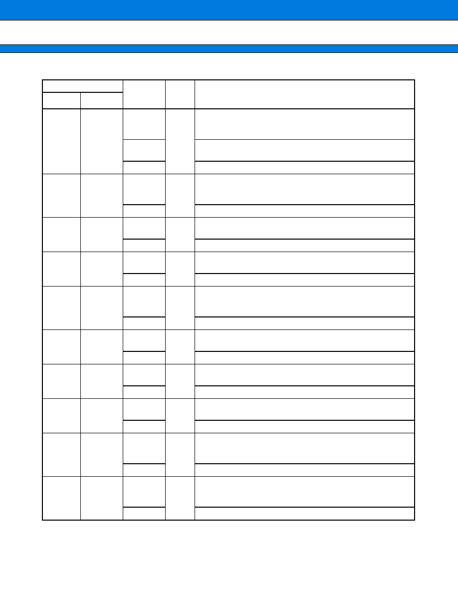
∑ MB91V301
(TOP VIEW)
(PGA-179C-A03)
A
B
C
D
E
F
G
H
J
K
L
M
N
P
INDEX
7
179
177
10
4
2
15
9
3
173
176
180
169
171
175
166
167
170
1
162
163
164
157
159
158
154
153
152
149
147
146
148
143
141
144
138
135
139
137
131
134
132
128
136
16
13
8
6
20
14
12
21
19
18
11
17
25
22
24
23
26
27
28
29
30
31
32
35
33
34
36
37
38
41
40
46
45
39
42
47
48
43
44
49
54
50
52
55
60
53
58
61
57
59
65
63
62
64
66
69
68
51
56
67
70
73
74
80
85
72
71
77
76
75
81
79
78
86
90
96
91
101
107
113
119
125
130
83
82
92
93
98
102
108
114
118
122
126
87
84
94
99
103
104
109
112
117
121
124
89
88
R
133
1
2
3
4
5
6
7
8
9
10
11
12
13
14
15
5
178
174
172
168
165
161
160
156
155
151
150
145
142
140
129
127
100
105
106
110
111
115
116
120
123
97
95
MB91301/MB91V301
7
∑
∑
∑
∑
MB91V301 Pin No. Table
(Continued)
No.
PIN
Pin Name
No.
PIN
Pin Name
No.
PIN
Pin Name
1
E5
N.C.
36
C11
RD
71
J15
A15
2
C3
P13/D11
37
A12
DQMUU/WR0 (UUB) 72
J14
V
SS
3
C4
V
SS
38
B12
P85/DQMUL/WR1 (ULB) 73
J13
V
CC
4
B3
V
CC
39
A13
P86/DQMLU/WR2 (LUB) 74
J12
P60/A16
5
A1
P14/D12
40
D11
P87/DQMLL/WR3 (LLB) 75
K15
P61/A17
6
D5
P15/D13
41
C12
V
SS
76
K14
P62/A18
7
A2
P16/D14
42
B13
V
CC
77
K13
P63/A19
8
C5
P17/D15
43
A14
P90/SYSCLK
78
L15
P64/A20
9
B4
V
SS
44
B14
P91/MCLKE
79
L14
P65/A21
10
A3
V
CC
45
D12
P92/MCLK
80
K12
P66/A22
11
D6
P20/D16
46
E11
P93
81
L13
P67/A23
12
C6
P21/D17
47
C13
V
SS
82
M15
V
CC
13
B5
P22/D18
48
D13
V
CC
83
M14
V
CC
14
B6
P23/D19
49
C14
P94/SRAS/LABA/AS
84
N15
EWR3
15
A4
P24/D20
50
A15
P95/SCAS/BAA
85
L12
EWR2
16
A5
P25/D21
51
E12
P96/SWE/WR
86
M13
EWR1
17
D7
P26/D22
52
B15
V
SS
87
N14
EWR0
18
C7
P27/D23
53
E13
V
CC
88
P15
ECS
19
B7
V
SS
54
D14
A00
89
P14
EMRAM
20
A6
V
CC
55
C15
A01
90
M12
ICD3
21
A7
D24
56
F12
A02
91
L11
ICD2
22
B8
D25
57
F13
A03
92
N13
ICD1
23
D8
D26
58
E14
A04
93
N12
ICD0
24
C8
D27
59
F14
A05
94
P13
V
SS
25
A8
V
SS
60
D15
A06
95
R15
V
CC
26
A9
V
CC
61
E15
A07
96
M11
BREAK
27
B9
D28
62
G12
V
SS
97
R14
ICLK
28
C9
D29
63
G13
V
CC
98
N11
ICS2
29
D9
D30
64
G14
A08
99
P12
ICS1
30
A10
D31
65
F15
A09
100
R13
ICS0
31
B10
V
SS
66
G15
A10
101
M10
TRST
32
C10
V
CC
67
H14
A11
102
N10
C
33
A11
P80/RDY
68
H12
A12
103
P11
AV
CC
34
B11
P81/BGRNT
69
H13
A13
104
P10
AVRH
35
D10
P82/BRQ
70
H15
A14
105
R12
AVR
MB91301/MB91V301
8
No.
PIN
Pin Name
No.
PIN
Pin Name
No.
PIN
Pin Name
106
R11
AN3
141
L4
V
CC
176
D3
V
SS
107
M9
AN2
142
P1
V
SS
177
C2
V
CC
108
N9
AN1
143
L3
X0
178
B1
D08/P10
109
P9
AN0
144
M2
X1
179
B2
D09/P11
110
R10
AV
SS
/AVRL
145
N1
V
SS
180
D4
D10/P12
111
R9
INT0/PG0
146
K4
V
CC
112
P8
INT1/PG1
147
K3
MD0
113
M8
INT2/PG2
148
L2
MD1
114
N8
INT3/PG3
149
K2
MD2
115
R8
INT4/ATG/PG4
150
M1
V
CC
116
R7
INT5/SIN2/PG5
151
L1
V
CC
117
P7
INT6/SOT2/PG6
152
J4
INIT
118
N7
INT7/SCK2/PG7
153
J3
NMI
119
M7
V
CC
154
J2
V
SS
120
R6
SIN0/PJ0
155
K1
V
CC
121
P6
SOT0/PJ1
156
J1
CS0/PA0
122
N6
SCK0/PJ2
157
H2
CS1/PA1
123
R5
SIN1/PJ3
158
H4
CS2/PA2
124
P5
SOT1/PJ4
159
H3
CS3/PA3
125
M6
SCK1/PJ5
160
H1
CS4/TRG2/PA4
126
N5
PPG0/PJ6
161
G1
CS5/PPG2/PA5
127
R4
TRG0/PJ7
162
G2
CS6/PA6
128
P4
TIN0/PH0
163
G3
CS7/PA7
129
R3
TIN1/PPG3/PH1
164
G4
V
SS
130
M5
TIN2/TRG3/PH2
165
F1
V
CC
131
N4
V
SS
166
F2
D00/P00
132
P3
C
167
F3
D01/P01
133
R2
DREQ0/PB0
168
E1
D02/P02
134
P2
DACK0/PB1
169
E2
D03/P03
135
M4
DEOP0/PB2
170
F4
V
SS
136
L5
DREQ1/PB3
171
E3
V
CC
137
N3
DACK1/TRG1/PB4 172
D1
D04/P04
138
M3
DEOP1/PPG1/PB5 173
D2
D05/P05
139
N2
IOWR/PB6
174
C1
D06/P06
140
R1
IORD/PB7
175
E4
D07/P07
MB91301/MB91V301
9
s
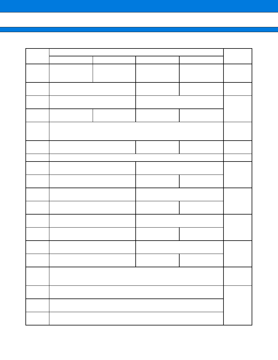
PIN DESCRIPTIONS
∑ Except for Power supply , GND, and Tool pins
(Continued)
Pin no.
Pin name
I/O
circuit
type
Function
MB91301
MB91V301
132 to 139
166 to 169,
172 to 175
D00 to D07
J
External data bus bits 0 to 7. It is available in the external bus
mode.
P00 to P07
Can be used as ports in 8-bit or 16-bit external bus mode.
142 to 144,
1 to 5
178 to 180,
2, 5 to 8
D08 to D15
J
External data bus bits 08 to 15. It is available in the external bus
mode.
P10 to P17
Can be used as ports in 8-bit or 16-bit external bus mode.
8 to 15
11 to 18
D16 to D23
J
External data bus bits 16 to 23. It is available in the external bus
mode.
P20 to P27
Can be used as ports in 8-bit external bus mode.
18 to 25
21 to 24,
27 to 30
D24 to D31
C
External data bus bits 24 to 31. It is available in the external bus
mode.
28
33
RDY
J
[RDY] External ready input. The pin has this function when
external ready input is enabled.
P80
[P80] General purpose input/output port. The pin has this
function when external ready input is disabled.
29
34
BGRNT
J
[BGRNT] Acknowledge output for external bus release.
Outputs "L" when the external bus is released. The pin has this
function when output is enabled.
P81
[P81] General purpose input/output port. The pin has this
function when output is disabled for external bus release
acknowledge.
30
35
BRQ
J
[BRQ] External bus release request input. Input "1" to request
release of the external bus. The pin has this function when input
is enabled.
P82
[P82] General purpose input/output port. The pin has this
function when the external bus release request input is disabled.
31
36
RD
C
[RD] External bus read strobe output.
32
37
WR0/ (UUB)
/DQMUU
C
[WR0] External bus write strobe output. When WR is used as the
write strobe, this becomes the byte-enable pin (UUB). Select
signal (DQMUU) of D31 to D24 at using of SDRAM.
33
38
WR1/ (ULB)
/DQMUL
J
[WR1] External bus write strobe output. The pin has this function
when WR1 output is enabled. When WR is used as the write
strobe, this becomes the byte-enable pin (ULB). Select signal
(DQMUL) of D23 to D16 at using of SDRAM.
P85
[P85] General purpose input/output port. The pin has this
function when the external bus write-enable output is disabled.
MB91301/MB91V301
10
(Continued)
Pin no.
Pin name
I/O
circuit
type
Function
MB91301 MB91V301
34
39
WR2/ (LUB)
/DQMLU
J
[WR2] External bus write strobe output. The pin has this function
when WR2 output is enabled. When WR is used as the write
strobe, this becomes the byte-enable pin (LUB). Select signal
(DQMLU) of D08 to D05 at using of SDRAM.
P86
[P86] General purpose input/output port. The pin has this function
when the external bus write-enable output is disabled.
35
40
WR3/ (LLB)
/DQMLL
J
[WR3] External bus write strobe output. The pin has this function
when WR3 output is enabled. When WR is used as the write
strobe, this becomes the byte-enable pin (LLB). Select signal
(DQMLL) of D07 to D00 at using of SDRAM.
P87
[P87] General purpose input/output port. The pin has this func-
tions when the external bus write-enable output is disabled.
36
43
SYSCLK
C
[SYSCLK] System clock output. The pin has this function when
system clock output is enabled. This outputs the same clock as
the external bus operating frequency. (Output halts in stop mode.)
P90
[P90] General purpose input/output port. The pin has this function
when system clock output is disabled.
37
40
MCLKE
J
[MCLKE] Clock enable signal for memory.
P91
[P91] General purpose input/output port. The pin has this function
when clock enable output is disabled.
38
45
MCLK
C
[MCLK] Memory clock output. The pin has this function when
memory clock output is enabled. This outputs the same clock as
the external bus operating frequency. (Output halts in sleep
mode.)
P92
[P92] General purpose input/output port. The pin has this function
when memory clock output is disabled.
39
46
P93
C
[P93] General purpose input/output port.
40
49
AS
J
[AS] Address strobe output. The pin has this function when ASE
bit of port function register 9 is enabled "1".
LBA
[LBA] Address strobe output for burst flash ROM. The pin has this
function when ASE bit of port function register 9 is enabled "1".
SRAS
[SRAS] RAS single for SDRAM. This pin has this function when
ASE bit of port function register 9 is enabled "1".
P94
[P94] General purpose input/output port. The pin has this function
when ASE bit of port function register 9 is "0" general purpose
port.
41
50
BAA
J
[BAA] Address advance output for burst Flash ROM. The pin has
this function when BAAE bit of port function register is enabled.
SCAS
[SCAS] CAS signal for SDRAM. This pin has this function when
BAAE bit of port function register is enabled.
P95
[P95] General purpose input/output port. The pin has this function
when BAAE bit of port function register is general purpose port.
MB91301/MB91V301
11
(Continued)
Pin no.
Pin name
I/O
circuit
type
Function
MB91301 MB91V301
42
51
WR
J
[WR] Memory write strobe output. This pin has this function when
WEXE bit of port function register is enabled.
SWE
[SWE] Write output for SDRAM. This pin has this function when
WEXE bit of port function register is enabled.
P96
[P96] General purpose input/output port. This pin has this function
when WEXE bit of port function register is general purpose port.
45 to 52
54 to 61
A00 to A07
C
External address bit 0 to 7.
55 to 62
64 to 71
A08 to A15
C
External address bit 8 to 15.
64 to 71
74 to 81
A16 to A23
J
External address bit 16 to 23. It is available in external bus mode.
P60 to P67
Can be used as ports when external address bus is not used.
76 to 79
106 to 109
AN3 to
AN0
D
Analog input pin.
81 to 84
111 to 114
INT0 to
INT3
L
[INT0 to INT3] External interrupt inputs. These inputs are used
continuously when the corresponding external interrupt is en-
abled. In this case, do not output to these ports unless doing so
intentionally.
PG0 to
PG3
[PG0 to PG3] General purpose input/output ports.
85
115
INT4
L
[INT4] External interrupt input. These inputs are used continuously
when the corresponding external interrupt is enabled. In this case,
do not output to these ports unless doing so intentionally.
ATG
[ATG] External trigger input for A/D converter. This input is used
continuously when selected as the A/D converter start trigger. In
this case, do not output to this port unless doing so intentionally.
PG4
[PG4] General purpose input/output ports.
86
116
INT5
L
[INT5] External interrupt input. These inputs are used continuously
when the corresponding external interrupt is enabled. In this case,
do not output to these ports unless doing so intentionally.
SIN2
[SIN2] UART2 data input pin. This input is used continuously when
UART2 is performing input. In this case, do not output to this port
unless doing so intentionally.
PG5
[PG5] General purpose input/output port.
87
117
INT6
L
[INT6] External interrupt input. This input is used continuously
when the corresponding external interrupt is enabled. In this case,
do not output to these ports unless doing so intentionally.
SOT2
[SOT2] UART2 data output pin. The pin has this function when
UART2 data output is enabled.
PG6
[PG6] General purpose input/output port.
MB91301/MB91V301
12
(Continued)
Pin no.
Pin name
I/O
circuit
type
Function
MB91301 MB91V301
88
118
INT7
L
[INT7] External interrupt input. This input is used continuously
when the corresponding external interrupt is enabled. In this case,
do not output to these ports unless doing so intentionally.
SCK2
[SCK2] UART2 clock input/output pin. The pin has this function
when UART2 clock output is enabled.
PG7
[PG7] General purpose input/output port.
90
120
SIN0
K
[SIN0] UART0 data input pin. This input is used continuously when
UART0 is performing input. In this case, do not output to this port
unless doing so intentionally.
PJ0
[PJ0] General purpose input/output port.
91
121
SOT0
J
[SOT0] UART0 data output pin. The pin has this function when
UART0 data output is enabled.
PJ1
[PJ1] General purpose input/output port.
92
122
SCK0
K
[SCK0] UART0 clock input/output pin. The pin has this function
when UART0 clock output is enabled.
PJ2
[PJ2] General purpose input/output port.
93
123
SIN1
K
[SIN1] UART1 data input pin. This input is used continuously
when UART1 is performing input. In this case, do not output to this
port unless doing so intentionally.
PJ3
[PJ3] General purpose input/output port.
94
124
SOT1
J
[SOT1] UART1 data output pin. The pin has this function when
UART1 data output is enabled.
PJ4
[PJ4] General purpose input/output port.
95
125
SCK1
K
[SCK1] UART1 clock input/output pin. The pin has this function
when UART1 clock output is enabled.
PJ5
[PJ5] General purpose input/output port.
96
126
PPG0
J
[PPG0] PPG timer output. This pin has this function when PPG0
output is enabled.
PJ6
[PJ6] General purpose input/output port.
97
127
TRG0
J
[TRG0] External trigger input for PPG timer. This input is used
continuously when the corresponding timer input is enabled. In
this case, do not output to this port unless doing so intentionally.
PJ7
[PJ7] General purpose input/output port.
98
128
TIN0
J
[TIN0] Reload timer input. This input is used continuously when
the corresponding timer input is enabled. In this case, do not out-
put to this port unless doing so intentionally.
PH0
[PH0] General purpose input/output port.
MB91301/MB91V301
13
(Continued)
Pin no.
Pin name
I/O
circuit
type
Function
MB91301 MB91V301
99
129
TIN1
J
[TIN1] Reload timer input. This input is used continuously when
the corresponding timer input is enabled. In this case, do not out-
put to this port unless doing so intentionally.
PPG3
[PPG3] PPG timer output. The pin has this function when PPG3
output is enabled.
PH1
[PH1] General purpose input/output port.
100
130
TIN2
J
[TIN2] Reload timer input. This input is used continuously when
the corresponding timer input is enabled. In this case, do not out-
put to this port unless doing so intentionally.
TRG3
[TRG3] External trigger input for PPG timer. This input is used con-
tinuously when the corresponding timer input is enabled. In this
case, do not output to this port unless doing so intentionally.
PH2
[PH2] General purpose input/output port.
103
133
DREQ0
J
[DREQ0] External input for DMA transfer requests. This input is
used continuously when selected as a DMA activation trigger. In
this case, do not output to this port unless doing so intentionally.
PB0
[PB0] General purpose input/output port.
104
134
DACK0
J
[DACK0] External acknowledge output for DMA transfer requests.
The pin has this function when outputting DMA transfer request
acknowledgement is enabled.
PB1
[PB1] General purpose input/output port.
105
135
DEOP0
J
[DEOP0] Completion output for DMA external transfer. The pin
has this function when outputting DMA transfer completion is en-
abled.
PB2
[PB2] General purpose input/output port.
106
136
DREQ1
J
[DREQ1] DMA External input for DMA transfer requests. This input
is used continuously when selected as a DMA activation trigger. In
this case, do not output to this port unless doing so intentionally.
PB3
[PB3] General purpose input/output port. The pin has this function
when completion output and stop input are disabled for DMA
transfer.
107
137
DACK1
J
[DACK1] External acknowledge output for DMA transfer requests.
The pin has this function when outputting DMA transfer request
acknowledgement is enabled.
TRG1
[TRG1] External trigger input for PPG timer. This input is used con-
tinuously when the corresponding timer input is enabled. In this
case, do not output to this port unless doing so intentionally.
PB4
[PB4] General purpose input/output port.
MB91301/MB91V301
14
(Continued)
Pin no.
Pin name
I/O
circuit
type
Function
MB91301 MB91V301
108
138
DEOP1
J
[DEOP1] Completion output for DMA external transfer. The pin
has this function when outputting DMA transfer completion is en-
abled.
PPG1
[PPG1] PPG timer output. The pin has this function when PPG1
bit is enabled.
PB5
[PB5] General purpose input/output port.
109
139
IOWR
C
[IOWR] Write strobe output for DMA fly-by transfer. The pin has
this function when outputting a write strobe for DMA fly-by transfer
is enabled.
PB6
[PB6] General purpose input/output port. The pin has this function
when outputting a write strobe for DMA fly-by transfer is disabled.
110
140
IORD
J
[IORD] Read strobe output for DMA fly-by transfer. The pin has
this function when outputting a read strobe for DMA fly-by transfer
is disabled.
PB7
[PB7] General purpose input/output port. The pin has this function
when outputting a write strobe for DMA fly-by transfer is disabled.
112
143
X0
A
Clock (oscillation) input.
113
144
X1
A
Clock (oscillation) output.
116 to
118
147 to 149
MD0 to
MD2
C
[MD0 to MD2] Mode pins to 0 to 2. The levels applied to these pins
set the basic operating mode. Connect VCC or VSS.
119
152
INIT
C
External reset input (Reset to initialize settings) ("L" active)
120
053
NMI
M
NMI (Non Maskable Interrupt) input ("L" active)
122
156
CS0
J
[CS0] Chip select 0 output. The pin has this function when chip se-
lect 0 output is enabled.
PA0
[PA0] General purpose input/output port. The pin has this function
when chip select 0 output is disabled.
123
157
CS1
J
[CS1] Chip select 1 output. The pin has this function when chip se-
lect 1 output is enabled.
PA1
[PA1] General purpose input/output port. The pin has this function
when chip select 1 output is disabled.
124
158
CS2
J
[CS2] Chip select 2 output. The pin has this function when chip se-
lect 2 output are enabled.
PA2
[PA2] General purpose input/output port. The pin has this function
when chip select 2 output is disabled.
125
159
CS3
J
[CS3] Chip select 3 output. The pin has this function when chip se-
lect 3 output are enabled.
PA3
[PA3] General purpose input/output port. The pin has this function
when chip select 3 output is disabled.
MB91301/MB91V301
15
(Continued)
* : Shaded pins are only present on the MB91V301.
∑ Power supply and GND pins
Pin no.
Pin name
I/O
circuit
type
Function
MB91301 MB91V301
126
160
CS4
J
[CS4] Chip select 4 output. The pin has this function when chip se-
lect 4 output is enabled.
TRG2
[TRG2] External trigger input for PPG timer. This input is used con-
tinuously when the corresponding timer input is enabled. In this
case, do not output to this port unless doing so intentionally.
PA4
[PA4] General purpose input/output port. The pin has this function
when chip select 4 output is disabled.
127
161
CS5
J
[CS5] Chip select 5 output. The pin has this function when chip se-
lect 5 output are enabled.
PPG2
[PPG2] PPG timer output. The pin has this function when PPG2 bit
is enabled.
PA5
[PA5] General purpose input/output port. The pin has this function
when chip select 5 output and PPG timer outputare disabled.
128
162
CS6
J
[CS6] Chip select 6 output. The pin has this function when chip se-
lect 6 output is enabled.
PA6
[PA6] General purpose input/output port. The pin has this function
when chip select 6 output are disabled.
129
163
CS7
J
[CS7] Chip select 7 output. The pin has this function when chip se-
lect 7 output are enabled.
PA7
[PA7] General purpose input/output port. The pin has this function
when chip select 7 output is disabled.
Pin no.
Pin name
Function
MB91301
MB91V301
6, 16, 26, 43, 53,
63, 101, 114, 130,
140
3, 9, 19, 25, 31, 41, 47, 52,
62, 72, 94, 131, 142, 145,
154, 164, 170, 176
V
SS
GND pins.
Connect all pins at the same potential.
7, 17, 27, 44, 54,
72, 89, 111, 115,
121, 131, 141
4, 10, 20, 26, 32, 42, 48, 53,
63, 73, 82, 83, 95, 119, 141,
146, 150, 151, 155, 165,
171, 177
V
CC
3 V power supply pins.
Connect all pins at the same potential.
73
103
AV
CC
Analog power supply pin for A/D converter
74
104
AVRH
Reference power supply pin for A/D converter
75
105
AVR
Capacitor coupling pin for the A/D converter
80
110
AV
SS
/AVRL
Analog GND pin for A/D converter
1
OPEN
Open pin. Use at open
102
102, 132
C
Capacitor coupling pin for the internal regula-
tor
MB91301/MB91V301
16
∑ Tool pins
Pin no.
Pin name
I/O circuit
type
Function
MB91301
MB91V301
97
ICLK
S
Clock output
101
TRST
Q
Tool reset
98 to 100
ICS2 to
ICS0
N
Device status output (during TRC)
DSU4 operation status output (during
EML)
90 to 93
ICD3 to
ICD0
R
Trace information output (during TRC)
Program/data I/O (duuring EML)
96
BREAK
P
DSU4 break reqest input
89
EMRAM
O
Emulation memory detection
88
ECS
N
Chip select for emuration memory
84 to 87
EWR3 to
EWR0
N
Write strobe for emuration memory
MB91301/MB91V301
17
s
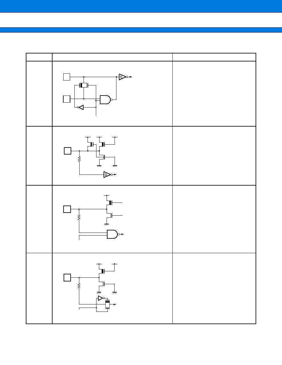
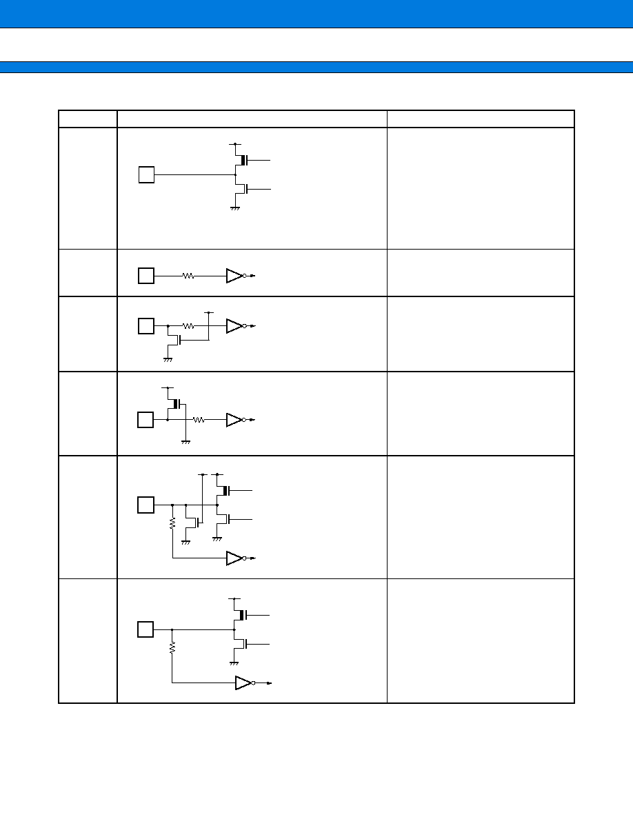
I/O CIRCUIT TYPE
(Continued)
Type
Circuit
Remarks
A
∑ Oscillation feedback resistance
approx. 1 M
B
∑ CMOS hysteresis input with pull-up
resistor
Pull-up resistor = 25 k
approx.
(Typ)
C
∑ CMOS level I/O with standby con-
trol
∑ I
OL
=
4 mA
D
∑ Analog input
With switch
X1
X0
Clock input
Standby control
Digital input
Digital input
Digital output
Digital output
Standby control
Analog input
Control
MB91301/MB91V301
18
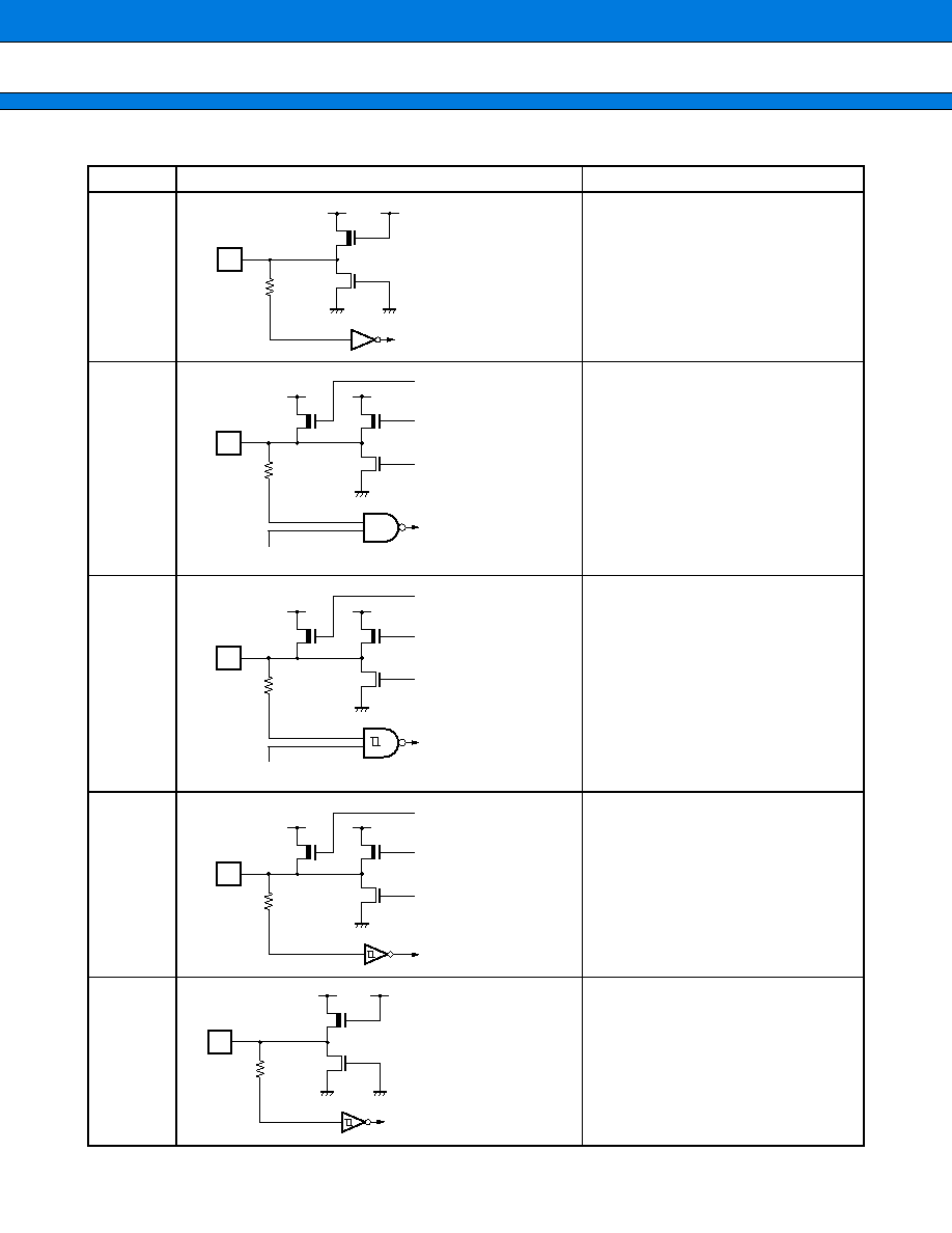
(Continued)
Type
Circuit
Remarks
G
∑ CMOS level output
No standby control
J
∑ With Pull-up control
Pull-up resistor value
=
25 k
approx. (Typ)
∑ CMOS level I/O
with standby control
∑ With Pull-up control
∑ I
OL
=
4 mA
K
∑ With Pull-up control
Pull-up resistor value
=
25 k
approx. (Typ)
∑ CMOS level output
CMOS level hysteresis input
with standby control
∑ I
OL
=
4 mA
L
∑ With Pull-up control
Pull-up resistor value
=
25 k
approx. (Typ)
∑ CMOS level output
CMOS level hysteresis input
no standby control
∑ I
OL
=
4 mA
M
∑ CMOS level hysteresis input
no standby control
Digital input
Digital output
Digital output
Digital input
Pull-up control
Standby control
Digital output
Digital output
Digital input
Pull-up control
Standby control
Digital output
Digital output
Digital input
Pull-up control
Digital input
MB91301/MB91V301
19
(Continued)
Type
Circuit
Remarks
N
∑ Output buffer
∑ CMOS level output
∑ I
OL
=
4 mA
O
∑ Input buffer
∑ CMOS level input
P
∑ Input buffer with pull-down
∑ Pull-down resistor value
=
25 k
approx. (Typ)
Q
∑ Input buffer with Pull-up
∑ Pull-up resistor value
=
25 k
approx. (Typ)
R
∑ I/O buffer with pull-down
∑ CMOS level output
∑ I
OL
=
4 mA
∑ Pull-up resistor value
=
25 k
approx. (Typ)
S
∑ I/O buffer
∑ CMOS level output
∑ I
OL
=
4 mA
Digital output
Digital output
Digital input
Digital input
Digital input
Digital input
Digital output
Digital output
Digital input
Digital output
Digital output
MB91301/MB91V301
20
s
HANDLING DEVICES
r
MB91301/MB91V301
∑
∑
∑
∑
Operation at start-up
Always apply a settings initialization (INIT) to the INIT pin immediately after turning on the power.
Also, in order to provide a delay while the oscillator circuits stabilize immediately after start-up, maintain the "L"
level input to the INIT pin for the required stabilization delay time. (The initialization processing (INIT) triggered
by the INIT pin initializes the oscillation stabilization delay time to the minimum setting.)
∑
∑
∑
∑
External clock input at start-up
At power-on start-up, always input a clock signal until the oscillation stabilization delay time is ended.
∑
∑
∑
∑
Output indeterminate at power-on time
When the power is turned on, the output pin may remain indeterminate until the internal power supply becomes
stable.
∑
∑
∑
∑
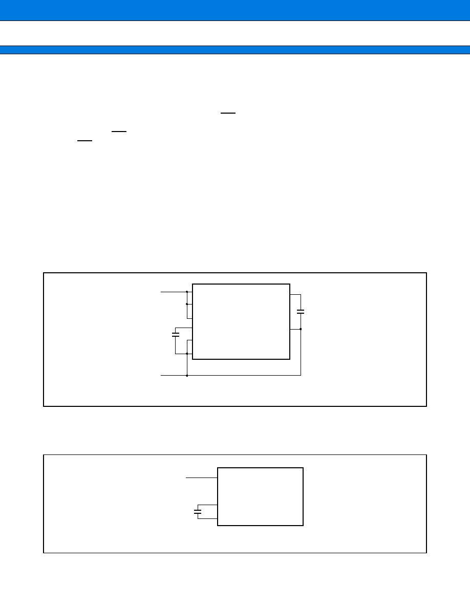
Built-in DC/DC regulator
This device has a built-in regulator, requiring 3.3 V input to the Vcc pin and a bypass capacitor of approximately
4.7
µ
F connected to the C pin for the regulator.
∑
∑
∑
∑
Note on use of the A/D converter
As the MB91301/MB91V301 contains an A/D converter, be sure to supply power to AVcc at 3.3 V and insert a
capacitor of at least 0.05
µ
F between the AVR pin and the AVss/AVRL pin.
3.3 V
V
CC
C
V
SS
AV
CC
AVR
AVRH
AV
SS
/AVRL
V
SS
GND
0.05
µ
F
4.7
µ
F
MB91301/MB91V301
Note of built-in DC/DC regulator
3.3 V
AV
CC
AVR
AVRH
AV
SS
/AVRL
0.05
µ
F
MB91301/
MB91V301
Note on Use of A/D Converter

MB91301/MB91V301
21
∑
∑
∑
∑
Preventing Latchup
When CMOS integrated circuit devices are subjected to applied voltages higher than V
CC
at input and output
pins, or to voltages lower than V
SS
, as well as when voltages in excess of rated levels are applied between V
CC
and V
SS
, a phenomenon known as latchup can occur. When a latchup condition occurs, the supply current can
increase dramatically and may destroy semiconductor elements. In using semiconductor devices, always take
sufficient care to avoid exceeding maximum ratings.
∑
∑
∑
∑
Power supply pins
Devices with multiple V
CC
and V
SS
supply pins are designed to prevent problems such as latchup occurring by
providing internal connections between pins at the same potential. However, in order to reduce unwanted
radiation, prevent abnormal operation of strobe signals due to a rise in ground level, and to maintain the total
output current ratings, all such pins should always be connected externally to power supply or ground. Also,
ensure that the impedance of the V
CC
and V
SS
connections to the power supply are as low as possible.
In addition, it is recommended that a bypass capacitor of approximately 0.1
µ
F be connected between V
CC
and
V
SS
. Connect the capacitor close to the V
CC
and V
SS
pins.
∑
∑
∑
∑
Crystal oscillators
Noise in proximity to the X0 and X1 pins can cause abnormal operation in this device. Printed circuit boards
should be designed so that the X0 and X1 pins, crystal (or ceramic) oscillator, and bypass capacitor connected
to ground are placed as close together as possible.
Also, to ensure stable operation, it is strongly recommended that the printed circuit board art work be designed
such that the X0 and X1 pins are surrounded by ground.
∑
∑
∑
∑
Treatment of NC and OPEN pins
Pins marked as "NC" or "OPEN" must be left open-circuit.
∑
∑
∑
∑
Treatment of unused input pins
If unused input pins are left open, abnormal operation may result. Any unused input pins should be connected
to pull-up or pull-down resistors.
∑
∑
∑
∑
Mode pins (MD0 to MD2)
These pins should be connected directly to V
CC
or V
SS
. To prevent the device erroneously switching to test mode
due to noise, design the printed circuit board such that the distance between the mode pins and V
CC
or V
SS
is
as short as possible and the connection impedance is low.
∑
∑
∑
∑
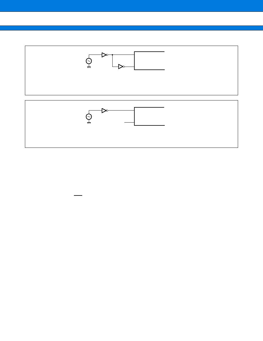
Remarks for External Clock Operation
When external clock is selected, supply it to X0 pin generally, and simultaneously the opposite phase clock to
X0 must be supplied to X1 pin. However, in this case the stop mode must not be used (because X1 pin stops at
"H" output in stop mode) .
When operating at 12.5 MHz or less, the microcontroller can be used with the clock signal supplied only to pin X0.
"Using an external clock (normal) and (12.5 MHz) " shows examples of how the MB91301 uses the external clock.
MB91301/MB91V301
22
∑
∑
∑
∑
Notes on during operation of PLL clock mode
If the PLL clock mode is selected, the microcontroller attempt to be working with the self-oscillating circuit even
when there is no external oscillator or external clock input is stopped. Performance of this operation, however,
cannot be guaranteed.
∑
∑
∑
∑
Clock control block
For L-level input to the INIT pin, allow for the regulator settling time or oscillation settling time.
∑
∑
∑
∑
Bit search module
The 0-detection, 1-detection, and transition-detection data registers (BSD0, BSD1, and BSDC) are only word-
accessible.
∑
∑
∑
∑
I/O port access
Byte access only for access to port
∑
∑
∑
∑
Shared port function switching
To switch a pin that also serves as a port, use the port function register (PFR). Note, however, that bus pins are
switched depending on external bus settings.
∑
∑
∑
∑
D-bus memory
Do not set a code area in D-bus memory.
No instruction fetch is performed to the D-bus.
Instruction fetches to the D-bus area result in incorrect data interpreted as code, which can cause the micro-
controller to lose control.
Do not set a data area in I-bus memory.
X0
X1
MB91301/MB91V301
Using an external clock (normal)
Note: Stop mode (oscillation stop mode) can not be used.
X0
X1
OPEN
MB91301/MB91V301
Using an external clock (12.5 MHz Max)

MB91301/MB91V301
23
∑
∑
∑
∑
I-bus memory
Do not set a stack area or vector table in I-bus memory.
It may cause a hang during EIT processing (including RETI).
Recovery from the hang requires a reset.
Do not perform DMA transfer to I-bus memory.
Do not access data in the instruction cache control register or the instruction cache RAM immediately before
the RETI instruction.
∑
∑
∑
∑
Low-power consumption modes
∑
To enter the standby mode, use the synchronous standby mode (set with the SYNCS bit as bit 8 in the
TBCR, or time-base counter control register) and be sure to use the following sequence:
(LDI
#value_of_standby, R0)
(LDI
#_STCR, R12)
STB
R0, @R12
; Write to standby control register (STCR)
LDUB
@R12, R0
; Read STCR for synchronous standby
LDUB
@R12, R0
; Read STCR again for dummy read
NOP
; NOP x 5 for timing adjustment
NOP
NOP
NOP
NOP
Set the I-flag and the ILM and ICR registers to branch to an interrupt handler when the interrupt handler
triggers the microcontroller to return from the standby mode.
∑
If you use the monitor debugger, follow the precautions below:
Do not set a breakpoint within the above array of instructions.
Do not single-step the above instructions.
∑
∑
∑
∑
Prefetch
When accessing a prefetch-enabled little endian area, use word access only (access in 32 bits).
Byte or halfword access results in wrong data read.
∑
∑
∑
∑
Terminal and timing control register (TCR)
The terminal and timing control register (TCR) is a write-only register. Do not therefore use a bit manipulation
instruction to access the TCR.
To disable bus sharing by setting the BREN bit as bit 7 in the TCR from 1 to 0, be sure to follow the procedure
below. Failure to follow it may hang the device.
1) Write 0 to the BRQE bit as bit 2 in the port-8 function register (PFR8).
2) Write 0 to the BREN bit as bit 7 in the TCR.
∑
∑
∑
∑
MCLK and SYSCLK
MCLK causes a stop in SLEEP/STOP mode while SYSCLK causes a stop only in STOP mode. Use either
depending on each application.

MB91301/MB91V301
24
∑
∑
∑
∑
Pull-up control
When function pins listed in the AC specifications (such as external bus control pins) have pull-up control,
enabling the pull-up resistor for a pin causes the actual pin load conditions to change. As all AC specifications
for this device were measured under the condition of pull-up resistors disabled, the values are not guaranteed
of AC specifications when pull-up resistors are enabled.
Even if the pull-up resistor is set to enabled for a pin, if the HIZ bit in the standby control register (STCR) specifies
setting output pins to high impedance during stop mode (HIZ
=
1) , changing to stop mode (STOP
=
1) causes
the pull-up resistor to be disabled.
∑
∑
∑
∑
R15 (General purpose register)
When any of the following instructions is executed, the SSP* or USP* value is not used as R15, resulting in an
incorrect value written to memory.
* : R15 is a virtual register. When a program attempts to access R15, the SSP or USP is accessed depending
on the status of the "S" flag as an SP flag. When coding the above ten instructions using an assembler,
specify a general-purpose register other than R15.
∑
∑
∑
∑
Notes on the PS register
Since some instructions manipulate the PS register earlier, the following exceptions may cause the interrupt
handler to break or the PS flag to update its display setting when the debugger is being used. As the microcon-
troller is designed to carry out reprocessing correctly upon returning from such an EIT event, it performs oper-
ations before and after the EIT as specified in either case.
∑
The following operations may be performed when the instruction immediately followed by a DIVOU/DIVOS
instruction is (a) halted by a user interrupt or NMI, (b) single-stepped, or (c) breaks in response to a data
event or emulator menu:
(1) D0 and D1 flags are updated earlier.
(2) The EIT handler (user interrupt/NMI or emulator) is executed.
(3) Upon returning from the EIT, the DIVOU/DIVOS instruction is executed and the D0 and D1 flags are
updated to the same values as those in (1) above.
∑
The following operations are performed when the ORCCR/STILM/MOV Ri and PS instructions are executed
to enable interruptions when a user interrupt or NMI trigger event has occurred.
(1) The PS register is updated earlier.
(2) The EIT handler (user interrupt/NMI or emulator) is executed.
(3) Upon returning from the EIT, the above instructions are executed and the PS register is updated to the
same value as that in (1) above.
∑
∑
∑
∑
A/D converter
When the device is turned on or returns from a reset or stop, it takes time for the external capacitor to be charged,
requiring the A/D converter to wait for at least 10 ms.
∑
∑
∑
∑
Watchdog timer
The watchdog timer function of this model monitors that a program delays a reset within a certain period of time
and resets the CPU if the program fails to delay it, for example, because the program runs out of control. Once
the watchdog timer function is enabled, therefore, the watchdog timer countinues to operate until a reset takes
place.
An exception, for example during stop, sleep and DMA transfer modes, is the automatic delaying of a reset under
a condition in which the CPU stops program execution.
Note, however, that a watchdog reset may not occur in the above state caused when the system runs out of
control. If this is the case, use the external INIT pin to cause a reset (INIT) .
AND
R15, @Ri
ANDH
R15, @Ri
ANDB
R15, @Ri
OR
R15, @Ri
ORH
R15, @Ri
ORB
R15, @Ri
EOR
R15, @Ri
EORH
R15, @Ri
EORB
R15, @Ri
XCHB
@Rj, R15
MB91301/MB91V301
25
r
Unique to the evaluation chip MB91V301
∑
∑
∑
∑
Tool reset
On an evaluation board, use the chip with INIT and TRST connected together.
∑
∑
∑
∑
Simultaneous occurrences of a software break and a user interrupt/NMI
When a software break and a user interrupt /NMI take place at the same time, the emulator debugger can cause
the following phenomena:
∑
The debugger stops pointing to a location other than the programmed breakpoints.
∑
The halted program is not re-executed correctly.
If these phenomena occur, use a hardware break instead of the software break. If the monitor debugger has
been used, avoid setting any break at the relevant location.
∑
∑
∑
∑
Single-stepping the RETI instruction
If an interrupt occurs frequently during single stepping, execute only the relevant processing routine repeatedly
after single-stepping RETI. This will prevent the main routine and low-interrupt-level programs from being
executed. Do not single-step the RETI instruction for avoidance purposes. When the debugging of the relevant
interrupt routine becomes unnecessary, perform debugging with that interrupt disabled.
∑
∑
∑
∑
Operand break
A stack pointer placed in an area set for a DSU operand break can cause a malfunction. Do not apply a data
event break to access to the area containing the address of a system stack pointer.
∑
∑
∑
∑
ICE startup sequence
When using the ICE, when you start debugging, ensure that the bus configuration is set correctly for the area
being used before downloading. After turning on the power to the target, the states of the RD and WR0 to WR3
pins are undefined until you perform the above setting. Accordingly, include enabling pull-up as part of the startup
sequence. If using these pins as general-purpose ports, set as output ports to prevent conflict with the output
signals during the time the pin states are undefined.
* : Use as output ports.
External bus width
Pin name
32 bit
16 bit
8 bit
RD
Pull-up
Pull-up
Pull-up
WR0
Pull-up
Pull-up
Pull-up
WR1 (P85)
Pull-up
Pull-up
*
WR2 (P86)
Pull-up
*
*
WR3 (P87)
Pull-up
*
*

MB91301/MB91V301
26
∑
∑
∑
∑
Configuration batch file
The example batch file below sets the mode vector and sets up the CS0 configuration register for the download
area. Use values appropriate to the hardware in the wait, timing, and other settings.
#---------------------------------------------------------
# Set MODR (0x7fd) =Enable In memory+16 bit External Bus
set mem/byte 0x7fd=0x5
#---------------------------------------------------------
# Set ASR0 (0x640) ; 0x0010_0000 - 0x002f_ffff
set mem/halfword 0x640=0x0010
#---------------------------------------------------------
# Set ACR0 (0x642)
#
; ASZ [3:0]=0101:2 MByte
#
; DBW [1:0]=01:16 bit width, automatically set from
MODR
#
; BST [1:0]=00:1 burst (16 bit x 2)
#
; SREN=0:Disable BRQ
#
; PFEN=1:Enable Pre fetch buffer
#
; WREN=1:Enable Write operation
#
; LEND=0: Big endian
#
; TYPE [3:0]=0010:WEX: Disable RDY
set mem/harfword 0x642=0x5462
#---------------------------------------------------------
# Set AWR0 (0x660)
#
; W15-12=0010:auto wait=2
#
; WR07, 06=01:RD, WR delay=1cycle
#
; W05, 04=01:WR->WR delay=1cycle (for WEX)
#
; W03 =1:MCLK->RD/WR delay=0.5cycle
#
;
:for async Memory
#
; W02 =0:ADR->CS delay=0
#
; W01 =0:ADR->RD/WR setup 0cycle
#
; W00 =RD/WR->ADR hold 0cycle
set mem/halfword 0x660=0x2058
#---------------------------------------------------------
MB91301/MB91V301
27
s
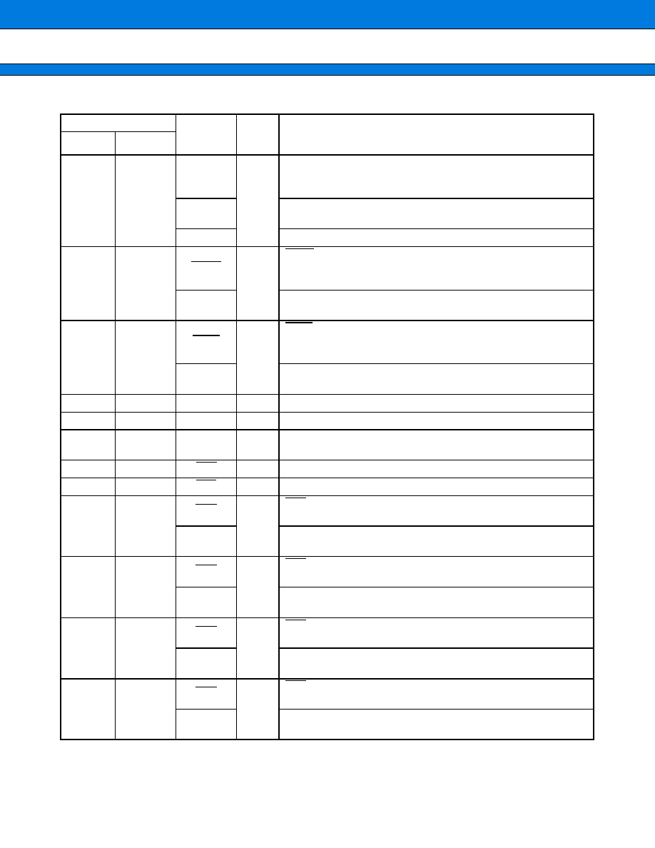
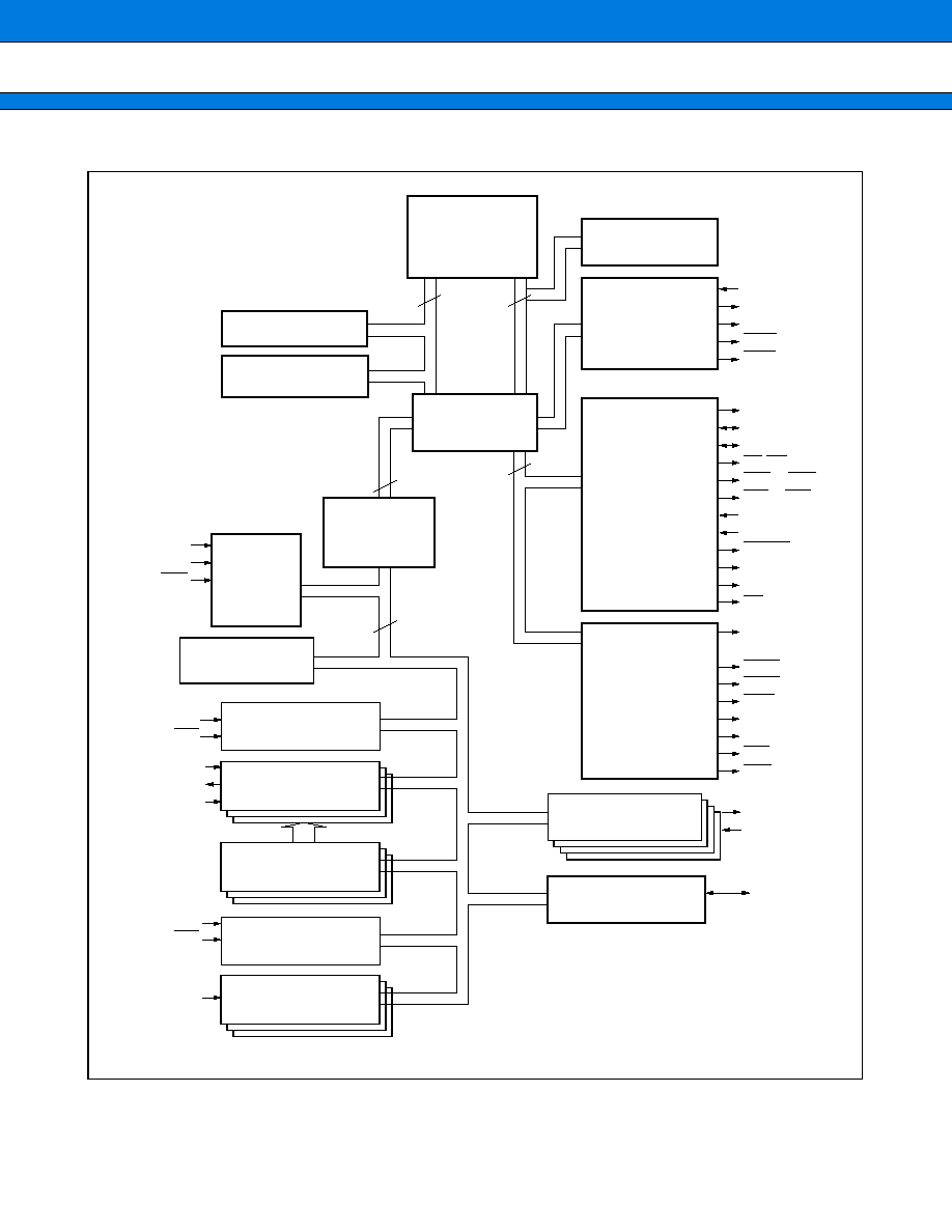
BLOCK DIAGRAM
I-Cache 4 KB
DMAC 5 ch
SDRAM I/F
PORT I/F
FR CPU
Core
Bus
Converter
32
32
32
32
32 to 16
Adapter
16
3 ch
UART
3 ch
U-TIMER
4 ch
A/D
X0, X1
MD0 to MD2
INIT
INT0 to INT7
NMI
SIN0 to SIN2
SOT0 to SOT2
SCK0 to SCK2
AN0 to AN3
AVR, ATG
AVRH, AV
CC
AV
SS
/AVRL
TIN0 to TIN2
DREQ0, DREQ1
DACK0, DACK1
DEOP0, DEOP1
IOWR
IORD
A23 to A00
D31 to D16
D15 to D0
RD, WR
WR0 to WR3
CS0 to CS7
RDY
BRQ
BGRNT
SYSCLK
MCLK
AS
MCLKE
SRAS
SCAS
SWE
DQMUU, L
DQMLU,L
LBA
BAA
PORT
PPG0 to PPG3
TRG0 to TRG3
Bit search
RAM 4 Kbytes
(stack)
Clock
control
Interrupt
controller
8 ch
External interrupts
4 ch
PPG timer
3 ch
Reload timer
External memory
I/F
MB91301/MB91V301
28
s
CPU
1.
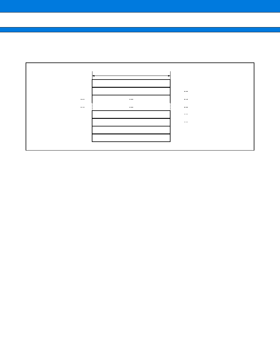
Memory Space
The FR family has 4 GB (2
32
addresses) of logical address space with linear access from the CPU.
∑
Direct Addressing Areas
The following areas of address space are used for I/O operations.
These areas are called direct addressing areas, in which the address of an operand can be specified directly
during an instruction.
The direct areas differ according to the size of the data accessed, as follows.
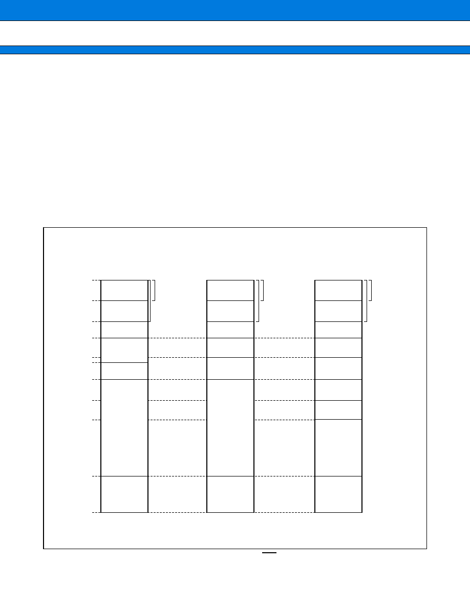
∑
Memory map
Note : Each mode is set depending on the mode vector fetch after INIT is negated. (For mode setting, see "
s
MODE
SETTINGS".)
byte data access
: 000
H
to 0FF
H
half word data access : 000
H
to 1FF
H
word data access
: 000
H
to 3FF
H
0000 0000
H
0000 0400
H
0001 0000
H
0002 0000
H
0003 E000
H
0003 F000
H
0004 0000
H
0004 2000
H
0006 0000
H
0010 0000
H
FFFF FFFF
H
I/O
I/O
I/O
I/O
I/O
I/O
I-RAM
I-RAM
I-RAM
* : On specific area between 10000
H
and 2000
H
, 4 Kbyte RAM can be used.
External ROM/
External bus mode
(volume production)
Direct
addressing
area
External
area
Internal RAM
4 Kbytes
Internal ROM/
External bus mode
(Evaluation product)
(at MODR register ROMA
=
1)
Access
prohibited
External ROM/
External bus mode
(Evaluation product)
(at MODR register ROMA
=
0)
External
area
External
area
External
area
External
area
External
area
Access
prohibited
Access
prohibited
Internal RAM
8 Kbytes
Internal RAM
8 Kbytes
See "
s
I/O MAP"
I/O
Internal RAM
8 Kbytes
Access
prohibited
Direct
addressing
area
Direct
addressing
area
See "
s
I/O MAP"
I/O
See "
s
I/O MAP"
I/O
MB91301/MB91V301
29
2.
Registers
The FR series has two types of registers: application-specific registers in the CPU and general purpose registers
in memory.
∑
Dedicated registers
∑
PC (Program Counter)
The PC is the program counter and stores the address of the currently executing instruction.
∑
Table base register (TBR)
The TBR is the table base register and stores the top address of the vector table used by the EIT function.
Program counter (PC)
: 32-bit register. Stores the current instruction address.
Program status (PS)
: 32-bit register. Contains the register pointer and condition code.
Table base register (TBR)
: Stores the top address of the vector table used by the EIT (exception/interrupt/
trap) function.
Return pointer (RP)
: Stores the subroutine return address.
System stack pointer (SSP) : Points to the system stack area.
User stack pointer (USP)
: Points to the user stack area.
Multiplication and division
result register (MDH/MDL)
: 32-bit registers used for multiplication and division.
PC
PS
TBR
RP
SSP
USP
MDH
MDL
XXXX XXXX
H
XXXX XXXX
H
XXXX XXXX
H
XXXX XXXX
H
XXXX XXXX
H
0000 0000
H
000F FC00
H
32 bit
Program counter
Program status
Table base register
Return pointer
System stack pointer
User stack pointer
Multiplication and division
result register
Initial value
PC
31
0
PC
TBR
31
0
TBR

MB91301/MB91V301
30
∑
Return pointer (RP)
The RP is the return pointer and stores the subroutine return address.
∑
System stack pointer (SSP)
The SSP is the system stack pointer and functions as R15 when the S flag is "0".
∑
User stack pointer (USP)
The USP is the user stack pointer and functions as R15 when the S flag is "1".
∑
Multiplication and division result register (MDH/MDL)
MDH/MDL : 32-bit registers used for multiplication and division.
MDH
: Remainder
MDL
: Quotient
RP
31
0
RP
SSP
31
0
SSP
USP
31
0
USP
Multiplication and division result register
31
0
MDH
MDL
MB91301/MB91V301
31
∑
Program status (PS)
This register holds the program status and is divided into the ILM, SCR, and CCR.
∑
Condition code register (CCR)
∑
System condition code register (SCR)
∑
Interrupt level mask register(ILM)
S flag
: Specifies which stack pointer to use as R15.
I flag
: Enables or disables user interrupt requests.
N flag
: Indicates the sign when an operation result is represented as a 2's complement integer.
Z flag
: Indicates whether an operation result is zero.
V flag
: Indicates whether an overflow occurred for an operation result when the operation operand is
represented as a 2's complement integer.
C flag
: Indicates whether an operation resulted in a borrow or a carry from the most significant bit.
D1, D0 flags
: Stores intermediate data for stepwise multiplication operations.
T flags
: A flag specifying whether the step trace trap function is enabled or not.
ILM4 to ILM0 : This register stores the interrupt level mask value. The value in the ILM register is used as
the level mask. Only interrupt requests to the CPU that have an interrupt level that is higher
than the level specified in ILM are accepted.
20
19
18
17
16
Initial Value
ILM4
ILM3
ILM2
ILM1
ILM0
Interrupt Level
01111
B
0
0
0
0
0
0
High
∑
∑
∑
∑
∑
∑
0
1
0
0
0
15
(Medium)
∑
∑
∑
∑
∑
∑
1
1
1
1
1
31
Low
ILM
Bit position
PS
31
20
16
ILM
SCR
CCR
10
7
8
0
Initial Value
- - 00XXXX
B
CCR
7
6
5
4
3
2
1
0
S
I
N
Z
V
C
Initial Value
XX0
B
SCR
10
9
8
D1
D0
T
MB91301/MB91V301
32
s
GENERAL PURPOSE REGISTERS
General purpose registers R0 to R15 are used by the CPU. The registers are used as the accumulator and
memory access pointers for CPU operations.
The following three registers are treated as having special meanings to enhance the operation of some instruc-
tions.
R13 : Virtual accumulator (AC)
R14 : Frame pointer (FP)
R15 : Stack pointer (SP)
The values of R0 to R14 after a reset are undefined. R15 is initialized to 0000 0000
H
(SSP value) .
R0
R1
R12
R13
R14
R15
AC (Accumulator)
FP (Frame Pointer)
SP (Stack Pointer)
XXXX XXXX
H
XXXX XXXX
H
0000 0000
H
Initial Value
32-bit
MB91301/MB91V301
33
s
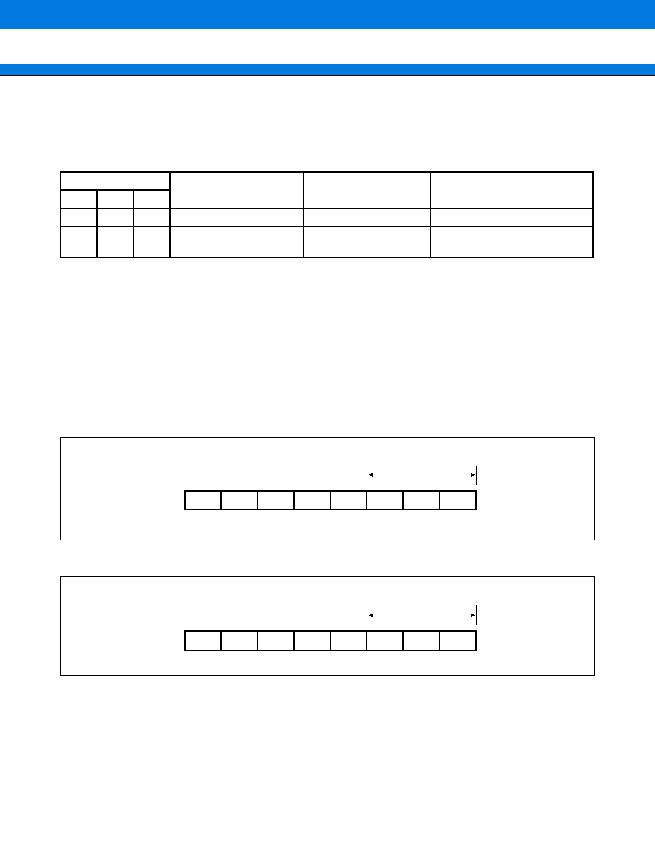
MODE SETTINGS
In the FR series, the mode is set by the mode pins (MD2, 1, 0) and mode register (MODR).
1.
Mode Pins
The MD2, MD1, and MD0 pins specify how the mode vector fetch is performed.
Values other than those listed in the table are prohibited.
* : Single-chip mode is not set.
2.
Mode Register (MODR)
∑ Details of mode register (MODR)
The data written to the mode register by the mode vector fetch operation (see "3.11.3 reset sequences") is
called the mode data.
After the data is set to the mode register (MODR), the device operates with the operating mode specified by
this data. The mode register is set by all types of reset. The register cannot be written to by user programs.
<Details of mode register (MODR) >
<Details of mode data>
[bit31 to bit27] Reserved bits
These bits should always be set to "00000." If set to any other value, stable operation is not assured.
Mode Pins
Mode name
Reset vector access
area
Remarks
MD2
MD1
MD0
0
0
0
Internal ROM vector mode
Internal
Single-chip mode*
0
0
1
External ROM vector mode
External
The bus width is specified by the
mode register.
bit
Initial Value
Address
XXXXXXXX
B
23
22
21
20
19
18
17
16
ROMA
WTH1
WTH0
W
W
W
Operation mode setting bits
bit
Initial Value
Address
XXXXXXXX
B
31
30
29
28
27
26
25
24
ROMA
WTH1
WTH0
W
W
W
Operation mode setting bits

MB91301/MB91V301
34
∑ Operating mode
∑ Bus mode
The bus mode controls the operations of internal ROM and the external access function. It is specified with
the mode setting pins (MD2, MD1, MD0) and the ROMA bit in mode data.
∑ Access mode
The access mode controls the external data bus width. It is specified with the WTH1 and WTH0 bits in the
mode register and the DBW1 and DBW0 bits in area configuration registers 0 to 7 (ACR0 to ACR7).
∑ Bus Modes
The FR family has three bus modes: bus mode 0 (single-chip mode), bus mode 1 (internal-ROM, external-bus
mode), and bus mode 2 (external-ROM, external-bus mode).
The MB91301 supports only bus mode 2 (external-ROM, external-bus mode).
See "Memory Space" in
s
CPU for details.
∑ Bus mode 2 (External-ROM, external-bus mode)
This mode enables internal I/O and D-bus RAM, in which any access is access to external space. Some
external pins serve as bus pins.
Bus mode
Access mode
32-bit bus width
External ROM, external bus
16-bit bus width
8-bit bus width
MB91301/MB91V301
35
s
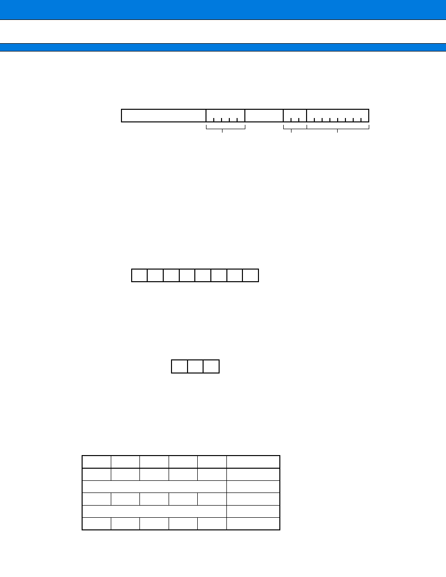
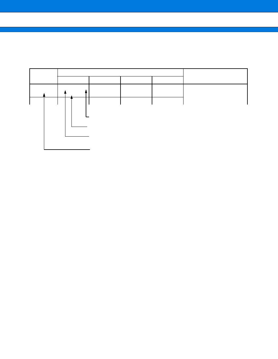
I/O MAP
This shows the location of the various peripheral resource registers in the memory space.
[How to read the table]
Note : Initial values of register bits are represented as follows :
"1" : Initial value"1"
"0" : Initial value"0"
"X" : Initial value"X"
"-"
: No physical register at this location
address
register
block
+
+
+
+
0
+
+
+
+
1
+
+
+
+
2
+
+
+
+
3
000000
H
PDR0 [R/W]
XXXXXXXX
PDR1 [R/W]
XXXXXXXX
PDR2 [R/W]
XXXXXXXX
PDR3 [R/W]
XXXXXXXX
T-unit
Port Data Register
Read/write attribute, Access type
Register name (Address of column 1 register is 4n, address of column
2 register is 4n+2, etc.)
Location of left-most register (When using word access,
the register in column 1 is in the MSB side of the data.)
Initial value after a reset
MB91301/MB91V301
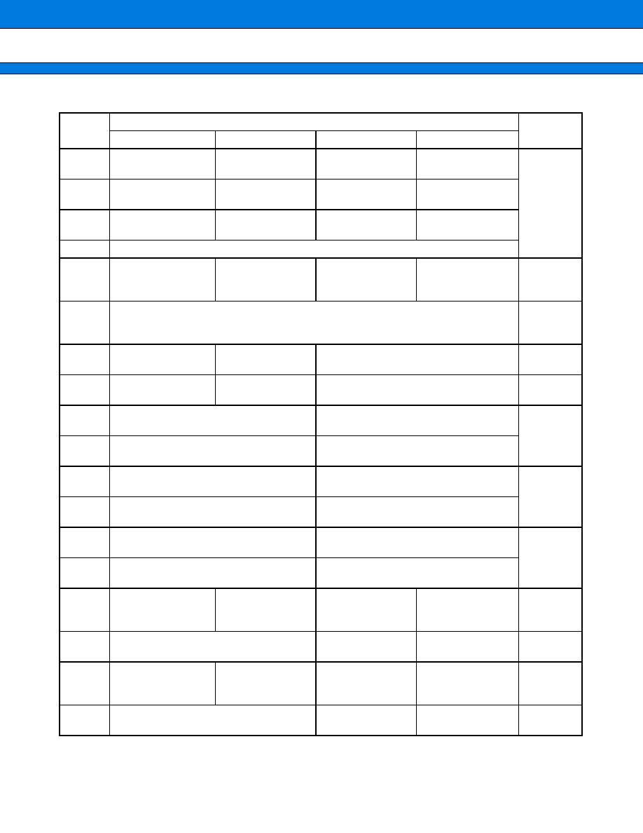
36
(Continued)
Address
Register
Block
+
+
+
+
0
+
+
+
+
1
+
+
+
+
2
+
+
+
+
3
000000
H
PDR0 [R/W] B
XXXXXXXX
PDR1 [R/W] B
XXXXXXXX
PDR2 [R/W] B
XXXXXXXX
T-unit
Port Data
Register
000004
H
PDR6 [R/W] B
XXXXXXXX
000008
H
PDR8 [R/W] B
XXXXXXXX
PDR9 [R/W] B
-
XXXXXXX
PDRA [R/W] B
XXXXXXXX
PDRB [R/W] B
XXXXXXXX
00000C
H
000010
H
PDRG [R/W] B
XXXXXXXX
PDRH [R/W] B
-
-
-
-
-
XXX
PDRJ [R/W] B
XXXXXXXX
R-bus
Port Data
Register
000014
H
to
00003C
H
Reserved
000040
H
EIRR [R/W] B, H, W
00000000
ENIR [R/W] B, H, W
00000000
ELVR [R/W] B, H, W
00000000
Ext int
000044
H
DICR [R/W] B, H, W
-
-
-
-
-
-
-
0
HRCL [R/W] B, H, W
0
-
-
11111
DLYI/I-unit
000048
H
TMRLR0 [W] H, W
XXXXXXXX XXXXXXXX
TMR0 [R] H, W
XXXXXXXX XXXXXXXX
Reload
Timer 0
00004C
H
TMCSR0 [R/W] B, H, W
-
-
XX0000 00000000
000050
H
TMRLR1 [W] H, W
XXXXXXXX XXXXXXXX
TMR1 [R] H, W
XXXXXXXX XXXXXXXX
Reload
Timer 1
000054
H
TMCSR1 [R/W] B, H, W
-
-
XX0000 00000000
000058
H
TMRLR2 [W] H, W
XXXXXXXX XXXXXXXX
TMR2 [R] H, W
XXXXXXXX XXXXXXXX
Reload
Timer 2
00005C
H
TMCSR2 [R/W] B, H, W
-
-
XX0000 00000000
000060
H
SSR0 [R/W] B, H, W
00001000
SIDR0 [R]
SODR0 [W] B, H, W
XXXXXXXX
SCR0 [R/W] B, H, W
00000100
SMR0 [R/W] B, H, W
00
-
-
0
-
0
-
UART0
000064
H
UTIM0 [R] H, W (UTIMR0 [W] H, W)
00000000 00000000
DRCL0 [W] B
-
-
-
-
-
-
-
-
UTIMC0 [R/W] B
0
-
-
00001
U-TIMER 0
000068
H
SSR1 [R/W] B, H, W
00001000
SIDR1 [R]
SODR1 [W] B, H, W
XXXXXXXX
SCR1 [R/W] B, H, W
00000100
SMR1 [R/W] B, H, W
00
-
-
0
-
0
-
UART1
00006C
H
UTIM1 [R] H, W (UTIMR1 [W] H, W )
00000000 00000000
DRCL1 [W] B
-
-
-
-
-
-
-
-
UTIMC1 [R/W] B
0
-
-
00001
U-TIMER 1
MB91301/MB91V301
37
(Continued)
Address
Register
Block
+
+
+
+
0
+
+
+
+
1
+
+
+
+
2
+
+
+
+
3
000070
H
SSR2 [R/W] B, H, W
00001000
SIDR2 [R]
SODR2 [W] B, H, W
XXXXXXXX
SCR2 [R/W] B, H, W
00000100
SMR2 [R/W] B, H, W
00
-
-
0
-
0
-
UART2
000074
H
UTIM2 [R] H, W (UTIMR2 [W] H, W )
00000000 00000000
DRCL2 [W] B
-
-
-
-
-
-
-
-
UTIMC2 [R/W] B
0
-
-
00001
U-TIMER 2
000078
H
ADCR [R] B, H, W
000000XX XXXXXXXX
ADCS [R/W] B, H, W
00000000 00000000
A/D
Converter
Sequential
Comparator
00007C
H
ADCR0 [R] B, H, W
XXXXXXXX
ADCR1 [R] B, H, W
XXXXXXXX
ADCR2 [R] B, H, W
XXXXXXXX
ADCR3 [R] B, H, W
XXXXXXXX
000080
H
to
000117
H
Reserved
000118
H
GCN10 [R/W] H
00110010 00010000
GCN20 [R/W] B
00000000
PPG timer
000011C
H
Reserved
000120
H
PTMR0 [R] H
11111111 11111111
PCSR0 [W] H, W
XXXXXXXX XXXXXXXX
PPG0
000124
H
PDUT0 [W] H, W
XXXXXXXX XXXXXXXX
PCNH0 [R/W] B
00000000
PCNL0 [R/W] B
000000X0
000128
H
PTMR1[R] H
11111111 11111111
PCSR1 [W] H, W
XXXXXXXX XXXXXXXX
PPG1
00012C
H
PDUT1 [W] H, W
XXXXXXXX XXXXXXXX
PCNH1 [R/W] B
00000000
PCNL1 [R/W] B
000000X0
000130
H
PTMR2 [R] H
11111111 11111111
PCSR2 [W] H, W
XXXXXXXX XXXXXXXX
PPG2
000134
H
PDUT2 [W] H, W
XXXXXXXX XXXXXXXX
PCNH2 [R/W] B
00000000
PCNL2 [R/W] B
000000X0
000138
H
PTMR3[R] H
11111111 11111111
PCSR3 [W] H, W
XXXXXXXX XXXXXXXX
PPG3
00013C
H
PDUT3 [W] H, W
XXXXXXXX XXXXXXXX
PCNH3 [R/W] B
00000000
PCNL3 [R/W] B
000000X0
000140
H
to
0001FC
H
Reserved
000200
H
DMACA0 [R/W] B, H, W*
1
00000000 0000XXXX XXXXXXXX XXXXXXXX
DMAC
000204
H
DMACB0 [R/W] B, H, W
00000000 00000000 XXXXXXXX XXXXXXXX
000208
H
DMACA1 [R/W] B, H, W*
1
00000000 0000XXXX XXXXXXXX XXXXXXXX
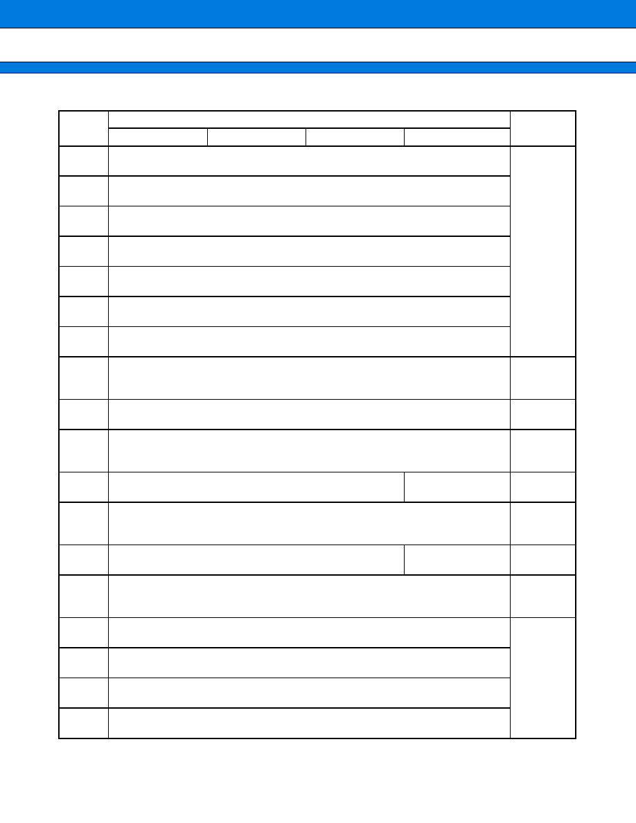
MB91301/MB91V301
38
(Continued)
Address
Register
Block
+
+
+
+
0
+
+
+
+
1
+
+
+
+
2
+
+
+
+
3
00020C
H
DMACB1 [R/W] B, H, W
00000000 00000000 XXXXXXXX XXXXXXXX
DMAC
000210
H
DMACA2 [R/W] B, H, W*
1
00000000 0000XXXX XXXXXXXX XXXXXXXX
000214
H
DMACB2 [R/W] B, H, W
00000000 00000000 XXXXXXXX XXXXXXXX
000218
H
DMACA3 [R/W] B, H, W*
1
00000000 0000XXXX XXXXXXXX XXXXXXXX
00021C
H
DMACB3 [R/W] B, H, W
00000000 00000000 XXXXXXXX XXXXXXXX
000220
H
DMACA4 [R/W] B, H, W*
1
00000000 0000XXXX XXXXXXXX XXXXXXXX
000224
H
DMACB4 [R/W] B, H, W
00000000 00000000 XXXXXXXX XXXXXXXX
000228
H
to
00023C
H
Reserved
000240
H
DMACR [R/W] B
0XX00000 XXXXXXXX XXXXXXXX XXXXXXXX
DMAC
000244
H
to
000300
H
Reserved
000304
H
ISIZE [R/W] B, H, W
-
-
-
-
-
-
10
I-Cache
000308
H
to
0003E0
H
Reserved
0003E4
H
ICHCR [R/W] B, H, W
0
-
000000
I-Cache
0003E8
H
to
0003EF
H
Reserved
0003F0
H
BSD0 [W] W
XXXXXXXX XXXXXXXX XXXXXXXX XXXXXXXX
Bit Search
Module
0003F4
H
BSD1 [R/W] W
XXXXXXXX XXXXXXXX XXXXXXXX XXXXXXXX
0003F8
H
BSDC [W] W
XXXXXXXX XXXXXXXX XXXXXXXX XXXXXXXX
0003FC
H
BSRR [R] W
XXXXXXXX XXXXXXXX XXXXXXXX XXXXXXXX
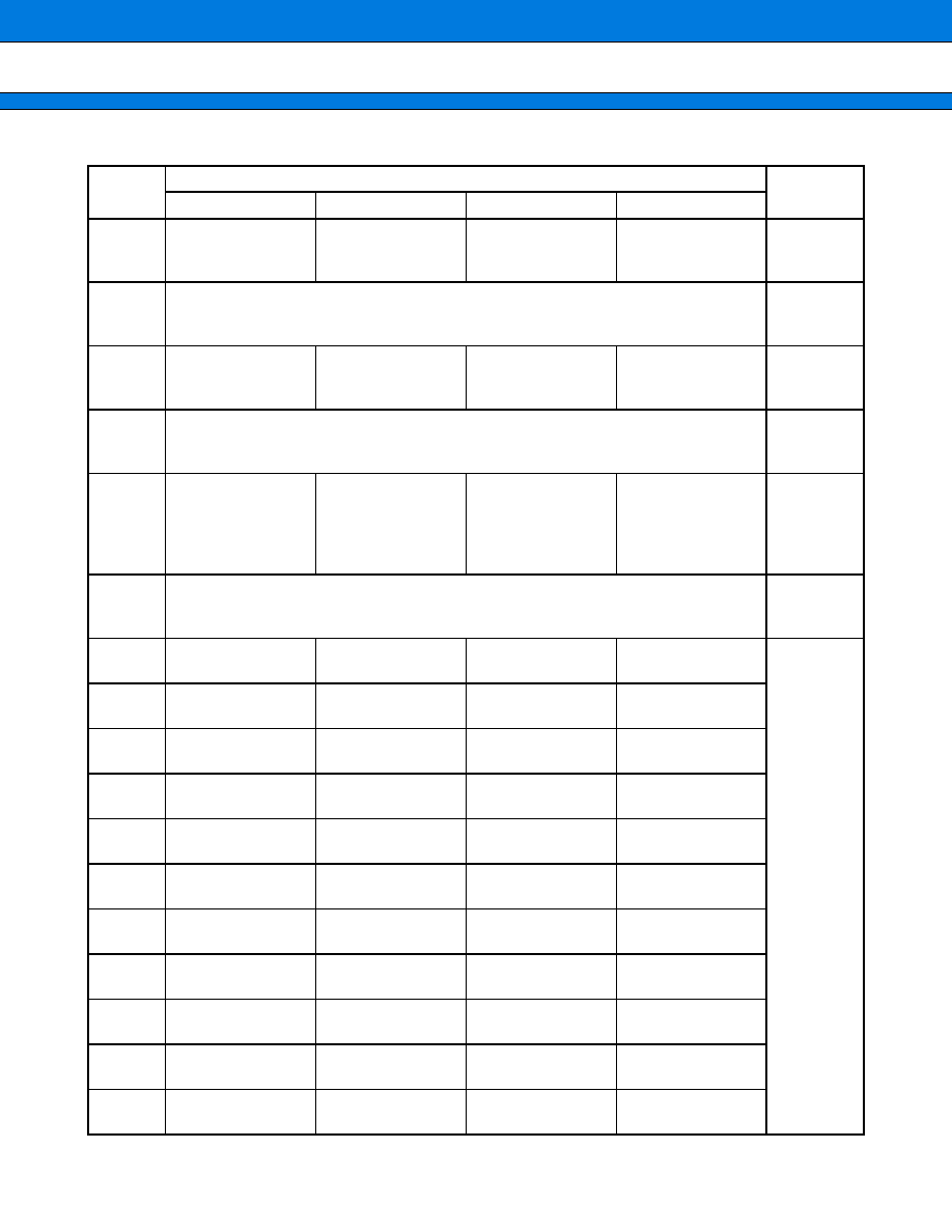
MB91301/MB91V301
39
(Continued)
Address
Register
Block
+
+
+
+
0
+
+
+
+
1
+
+
+
+
2
+
+
+
+
3
000400
H
DDRG [R/W] B
00000000
DDRH [R/W] B
-
-
-
-
-
000
DDRJ [R/W] B
00000000
R-bus Data
Direction
Register
000404
H
to
00040C
H
Reserved
000410
H
PFRG [R/W] B
00
-
-
-
-
-
-
PFRH [R/W] B
-
-
-
-
-
-
0
-
PFRJ [R/W] B
-
-
00
-
00
-
R-bus Port
Function
Register
000414
H
to
00041C
H
Reserved
000420
H
PCRG [R/W] B
00000000
PCRH [R/W] B
-
-
-
-
-
000
PCRJ [R/W] B
00000000
R-bus
Pull-up
Resistance
Control
Register
000424
H
to
00043C
H
Reserved
000440
H
ICR00 [R/W] B, H, W
-
-
-
11111
ICR01 [R/W] B, H, W
-
-
-
11111
ICR02 [R/W] B, H, W
-
-
-
11111
ICR03 [R/W] B, H, W
-
-
-
11111
Interrupt
Controller
000444
H
ICR04 [R/W] B, H, W
-
-
-
11111
ICR05 [R/W] B, H, W
-
-
-
11111
ICR06 [R/W] B, H, W
-
-
-
11111
ICR07 [R/W] B, H, W
-
-
-
11111
000448
H
ICR08 [R/W] B, H, W
-
-
-
11111
ICR09 [R/W] B, H, W
-
-
-
11111
ICR10 [R/W] B, H, W
-
-
-
11111
ICR11 [R/W] B, H, W
-
-
-
11111
00044C
H
ICR12 [R/W] B, H, W
-
-
-
11111
ICR13 [R/W] B, H, W
-
-
-
11111
ICR14 [R/W] B, H, W
-
-
-
11111
ICR15 [R/W] B, H, W
-
-
-
11111
000450
H
ICR16 [R/W] B, H, W
-
-
-
11111
ICR17 [R/W] B, H, W
-
-
-
11111
ICR18 [R/W] B, H, W
-
-
-
11111
ICR19 [R/W] B, H, W
-
-
-
11111
000454
H
ICR20 [R/W] B, H, W
-
-
-
11111
ICR21 [R/W] B, H, W
-
-
-
11111
ICR22 [R/W] B, H, W
-
-
-
11111
ICR23 [R/W] B, H, W
-
-
-
11111
000458
H
ICR24 [R/W] B, H, W
-
-
-
11111
ICR25 [R/W] B, H, W
-
-
-
11111
ICR26 [R/W] B, H, W
-
-
-
11111
ICR27 [R/W] B, H, W
-
-
-
11111
00045C
H
ICR28 [R/W] B, H, W
-
-
-
11111
ICR29 [R/W] B, H, W
-
-
-
11111
ICR30 [R/W] B, H, W
-
-
-
11111
ICR31 [R/W] B, H, W
-
-
-
11111
000460
H
ICR32 [R/W] B, H, W
-
-
-
11111
ICR33 [R/W] B, H, W
-
-
-
11111
ICR34 [R/W] B, H, W
-
-
-
11111
ICR35 [R/W] B, H, W
-
-
-
11111
000464
H
ICR36 [R/W] B, H, W
-
-
-
11111
ICR37 [R/W] B, H, W
-
-
-
11111
ICR38 [R/W] B, H, W
-
-
-
11111
ICR39 [R/W] B, H, W
-
-
-
11111
000468
H
ICR40 [R/W] B, H, W
-
-
-
11111
ICR41 [R/W] B, H, W
-
-
-
11111
ICR42 [R/W] B, H, W
-
-
-
11111
ICR43 [R/W] B, H, W
-
-
-
11111
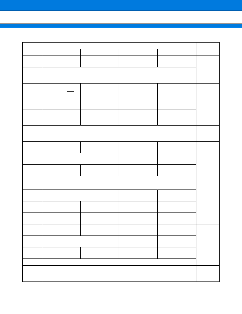
MB91301/MB91V301
40
(Continued)
Address
Register
Block
+
+
+
+
0
+
+
+
+
1
+
+
+
+
2
+
+
+
+
3
00046C
H
ICR44 [R/W] B, H, W
-
-
-
11111
ICR45 [R/W] B, H, W
-
-
-
11111
ICR46 [R/W] B, H, W
-
-
-
11111
ICR47 [R/W] B, H, W
-
-
-
11111
Interrupt
Controller
000470
H
to
00047C
H
000480
H
RSRR [R/W] B, H, W
10000000 (INIT)
-
0
-
XX
-
00 (INIT)
XXX
-
-
X00 (RST)
STCR [R/W] B, H, W
00110011 (INIT)
00111111 (HST)
0011XX11 (INIT)
00X1XXX (RST)
TBCR [R/W] B, H, W
00XXXX00 (INIT)
00XXXXXX (RST)
CTBR [W] B, H, W
XXXXXXXX (INIT)
XXXXXXXX (RST)
Clock
Control unit
000484
H
CLKR [R/W] B, H, W
00000000 (INIT)
XXXXXXXX (RST)
WPR [W] B, H, W
XXXXXXXX (INIT)
XXXXXXXX (RST)
DIVR0 [R/W] B, H, W
00000011 (INIT)
XXXXXXXX (RST)
DIVR1 [R/W] B, H, W
00000000 (INIT)
XXXXXXXX (RST)
000488
H
to
0005FC
H
Reserved
000600
H
DDR0 [R/W] B
00000000
DDR1 [R/W] B
00000000
DDR2 [R/W] B
00000000
T-unit
Data
Direction
Register
000604
H
DDR6 [R/W] B
00000000
000608
H
DDR8 [R/W] B
00000000
DDR9 [R/W] B
-
0000000
DDRA [R/W] B
00000000
DDRB [R/W] B
00000000
00060C
H
000610
H
T-unit
Port
Function
Register
000614
H
PFR6 [R/W] B
11111111
000618
H
PFR8 [R/W] B
111
-
-
0
-
-
PFR9 [R/W] B
-
0000111
PFRA1 [R/W] B
11111111
PFRB1 [R/W] B
00000000
00061C
H
PFRB2 [R/W] B
000
-
-
-
00
PFRA2 [R/W] B
-
-
0
-
-
-
-
-
000620
H
PCR0 [R/W] B
00000000
PCR1 [R/W] B
00000000
PCR2 [R/W] B
00000000
T-unit
Pull-up
Resistance
Control
Register
000624
H
PCR6 [R/W] B
00000000
000628
H
PCR8 [R/W] B
00000000
PCR9 [R/W] B
-
000
-
-
0
-
PCRA [R/W] B
00000000
PCRB [R/W] B
00000000
00062C
H
000630
H
to
00063C
H
Reserved
MB91301/MB91V301
41
(Continued)
Address
Register
Block
+
+
+
+
0
+
+
+
+
1
+
+
+
+
2
+
+
+
+
3
000640
H
ASR0 [R/W] H, W
00000000 00000000
ACR0 [R/W] H, W
1111XX00 00000000
T-unit
000644
H
ASR1 [R/W] H, W
XXXXXXXX XXXXXXXX
ACR1 [R/W] B, H, W
XXXXXXXX XXXXXXXX
000648
H
ASR2 [R/W] H, W
XXXXXXXX XXXXXXXX
ACR2 [R/W] B, H, W
XXXXXXXX XXXXXXXX
00064C
H
ASR3 [R/W] H, W
XXXXXXXX XXXXXXXX
ACR3 [R/W] B, H, W
XXXXXXXX XXXXXXXX
000650
H
ASR4 [R/W] H, W
XXXXXXXX XXXXXXXX
ACR4 [R/W] B, H, W
XXXXXXXX XXXXXXXX
000654
H
ASR5 [R/W] H, W
XXXXXXXX XXXXXXXX
ACR5 [R/W] B, H, W
XXXXXXXX XXXXXXXX
000658
H
ASR6 [R/W] H, W
XXXXXXXX XXXXXXXX
ACR6 [R/W] B, H, W
XXXXXXXX XXXXXXXX
00065C
H
ASR7 [R/W] H, W
XXXXXXXX XXXXXXXX
ACR7 [R/W] B, H, W
XXXXXXXX XXXXXXXX
000660
H
AWR0 [R/W] B, H, W
01111111 11111011
AWR1 [R/W] B, H, W
XXXXXXXX XXXXXXXX
000664
H
AWR2 [R/W] B, H, W
XXXXXXXX XXXXXXXX
AWR3 [R/W] B, H, W
XXXXXXXX XXXXXXXX
000668
H
AWR4 [R/W] B, H, W
XXXXXXXX XXXXXXXX
AWR5 [R/W] B, H, W
XXXXXXXX XXXXXXXX
00066C
H
AWR6 [R/W] B, H, W
XXXXXXXX XXXXXXXX
AWR7 [R/W] B, H, W
XXXXXXXX XXXXXXXX
000670
H
MCRA [R/W] B, H, W
XXXXXXXX
MCRB [R/W] B, H, W
XXXXXXXX
000674
H
000678
H
IOWR0 [R/W] B, H,
W
XXXXXXXX
IOWR1 [R/W] B, H,
W
XXXXXXXX
IOWR2 [R/W] B, H, W
XXXXXXXX
00067C
H
000680
H
CSER [R/W] B, H, W
00000001
CHER [R/W] B, H,
W
11111111
TCR [R/W] B, H, W
00000000 (INIT)
0000XXXX (RST)
000684
H
RCR [R/W] B, H, W
00XXXXXX XXXX0XXX
00068C
H
to
0007F8
H
Reserved
0007FC
H
MODR [W] *
2
XXXXXXXX
T-unit
MB91301/MB91V301
42
(Continued)
Address
Register
Block
+
+
+
+
0
+
+
+
+
1
+
+
+
+
2
+
+
+
+
3
000800
H
to
000AFC
H
Reserved
000B00
H
ESTS0 [R/W] B
X0000000
ESTS1 [R/W] B
XXXXXXXX
ESTS2 [R] B
1XXXXXXX
DSU
(Evaluation
chip only)
000B04
H
ECTL0 [R/W] B
0X000000
ECTL1 [R/W] B
00000000
ECTL2 [W] B
000X0000
ECTL3 [R/W] B
00X00X11
000B08
H
ECNT0 [W] B
XXXXXXXX
ECNT1 [W] B
XXXXXXXX
EUSA [W] B
XXX00000
EDTC [W] B
0000XXXX
000B0C
H
EWPT [R] H
00000000 00000000
ECTL4 [R] ([R/W]) B
-
0X00000
ECTL5 [R] ([R/W]) B
-
-
-
-
000X
000B10
H
EDTR0 [W] H
XXXXXXXX XXXXXXXX
EDTR1 [W] H
XXXXXXXX XXXXXXXX
000B14
H
to
000B1C
H
000B20
H
EIA0 [W] W
XXXXXXXX XXXXXXXX XXXXXXXX XXXXXXXX
000B24
H
EIA1 [W] W
XXXXXXXX XXXXXXXX XXXXXXXX XXXXXXXX
000B28
H
EIA2 [W] W
XXXXXXXX XXXXXXXX XXXXXXXX XXXXXXXX
000B2C
H
EIA3 [W] W
XXXXXXXX XXXXXXXX XXXXXXXX XXXXXXXX
000B30
H
EIA4 [W] W
XXXXXXXX XXXXXXXX XXXXXXXX XXXXXXXX
000B34
H
EIA5 [W] W
XXXXXXXX XXXXXXXX XXXXXXXX XXXXXXXX
000B38
H
EIA6 [W] W
XXXXXXXX XXXXXXXX XXXXXXXX XXXXXXXX
000B3C
H
EIA7 [W] W
XXXXXXXX XXXXXXXX XXXXXXXX XXXXXXXX
000B40
H
EDTA [R/W] W
XXXXXXXX XXXXXXXX XXXXXXXX XXXXXXXX
000B44
H
EDTM [R/W] W
XXXXXXXX XXXXXXXX XXXXXXXX XXXXXXXX
000B48
H
EOA0 [W] W
XXXXXXXX XXXXXXXX XXXXXXXX XXXXXXXX
000B4C
H
EOA1 [W] W
XXXXXXXX XXXXXXXX XXXXXXXX XXXXXXXX
000B50
H
EPCR [R/W] W
XXXXXXXX XXXXXXXX XXXXXXXX XXXXXXXX
MB91301/MB91V301
43
(Continued)
*1 : Byte access is not permitted for the lower 16 bits of DMAC0 to DMAC4 (DTC15 to DTC0) .
*2 : This register is accessed through mode vector fetch; it cannot be accessed in normal mode.
Address
Register
Block
+
+
+
+
0
+
+
+
+
1
+
+
+
+
2
+
+
+
+
3
000B54
H
EPSR [R/W] W
XXXXXXXX XXXXXXXX XXXXXXXX XXXXXXXX
000B58
H
EIAM0 [W] W
XXXXXXXX XXXXXXXX XXXXXXXX XXXXXXXX
000B5C
H
EIAM1 [W] W
XXXXXXXX XXXXXXXX XXXXXXXX XXXXXXXX
000B60
H
EOAM0/EODM0 [W] W
XXXXXXXX XXXXXXXX XXXXXXXX XXXXXXXX
000B64
H
EOAM1/EODM1 [W] W
XXXXXXXX XXXXXXXX XXXXXXXX XXXXXXXX
000B68
H
EOD0 [W] W
XXXXXXXX XXXXXXXX XXXXXXXX XXXXXXXX
000B6C
H
EOD1 [W] W
XXXXXXXX XXXXXXXX XXXXXXXX XXXXXXXX
000B70
H
to
000FFC
H
Reserved
001000
H
DMASA0 [R/W] W
XXXXXXXX XXXXXXXX XXXXXXXX XXXXXXXX
DMAC
001004
H
DMADA0 [R/W] W
XXXXXXXX XXXXXXXX XXXXXXXX XXXXXXXX
001008
H
DMASA1 [R/W] W
XXXXXXXX XXXXXXXX XXXXXXXX XXXXXXXX
00100C
H
DMADA1 [R/W] W
XXXXXXXX XXXXXXXX XXXXXXXX XXXXXXXX
001010
H
DMASA2 [R/W] W
XXXXXXXX XXXXXXXX XXXXXXXX XXXXXXXX
001014
H
DMADA2 [R/W] W
XXXXXXXX XXXXXXXX XXXXXXXX XXXXXXXX
001018
H
DMASA3 [R/W] W
XXXXXXXX XXXXXXXX XXXXXXXX XXXXXXXX
00101C
H
DMADA3 [R/W] W
XXXXXXXX XXXXXXXX XXXXXXXX XXXXXXXX
001020
H
DMASA4 [R/W] W
XXXXXXXX XXXXXXXX XXXXXXXX XXXXXXXX
001024
H
DMADA4 [R/W] W
XXXXXXXX XXXXXXXX XXXXXXXX XXXXXXXX
001028
H
to
001FFC
H
Reserved
MB91301/MB91V301
44
s
INTERRUPT VECTORS
(Continued)
Interrupt
Interrupt No.
Interrupt
level*
1
Offset
TBR default
address*
2
RN
10
16
Reset
0
00
3FC
H
000FFFFC
H
Mode vector
1
01
3F8
H
000FFFF8
H
System reserved
2
02
3F4
H
000FFFF4
H
System reserved
3
03
3F0
H
000FFFF0
H
System reserved
4
04
3EC
H
000FFFEC
H
System reserved
5
05
3E8
H
000FFFE8
H
System reserved
6
06
3E4
H
000FFFE4
H
Coprocessor absent trap
7
07
3E0
H
000FFFE0
H
Coprocessor error trap
8
08
3DC
H
000FFFDC
H
INTE instruction
9
09
3D8
H
000FFFD8
H
Instruction break exception
10
0A
3D4
H
000FFFD4
H
Operand break trap
11
0B
3D0
H
000FFFD0
H
Step trace trap
12
0C
3CC
H
000FFFCC
H
NMI request (tool)
13
0D
3C8
H
000FFFC8
H
Undefined instruction exception
14
0E
3C4
H
000FFFC4
H
NMI request
15
0F
15 (F
H
)
fixed
3C0
H
000FFFC0
H
External interrupt 0
16
10
ICR00
3BC
H
000FFFBC
H
6
External interrupt 1
17
11
ICR01
3B8
H
000FFFB8
H
7
External interrupt 2
18
12
ICR02
3B4
H
000FFFB4
H
11
External interrupt 3
19
13
ICR03
3B0
H
000FFFB0
H
12
External interrupt 4
20
14
ICR04
3AC
H
000FFFAC
H
External interrupt 5
21
15
ICR05
3A8
H
000FFFA8
H
External interrupt 6
22
16
ICR06
3A4
H
000FFFA4
H
External interrupt 7
23
17
ICR07
3A0
H
000FFFA0
H
Reload timer 0
24
18
ICR08
39C
H
000FFF9C
H
8
Reload timer 1
25
19
ICR09
398
H
000FFF98
H
9
Reload timer 2
26
1A
ICR10
394
H
000FFF94
H
10
UART0 (RX completed)
27
1B
ICR11
390
H
000FFF90
H
0
UART1 (RX completed)
28
1C
ICR12
38C
H
000FFF8C
H
1
UART2 (RX completed)
29
1D
ICR13
388
H
000FFF88
H
2
UART0 (TX completed)
30
1E
ICR14
384
H
000FFF84
H
3
UART1 (TX completed)
31
1F
ICR15
380
H
000FFF80
H
4
UART2 (TX completed)
32
20
ICR16
37C
H
000FFF7C
H
5
MB91301/MB91V301
45
(Continued)
Interrupt
Interrupt No.
Interrupt
level*
1
Offset
TBR default
address*
2
RN
10
16
DMAC0 (end, error)
33
21
ICR17
378
H
000FFF78
H
DMAC1 (end, error)
34
22
ICR18
374
H
000FFF74
H
DMAC2 (end, error)
35
23
ICR19
370
H
000FFF70
H
DMAC3 (end, error)
36
24
ICR20
36C
H
000FFF6C
H
DMAC4 (end, error)
37
25
ICR21
368
H
000FFF68
H
A/D
38
26
ICR22
364
H
000FFF64
H
15
PPG0
39
27
ICR23
360
H
000FFF60
H
13
PPG1
40
28
ICR24
35C
H
000FFF5C
H
14
PPG2
41
29
ICR25
358
H
000FFF58
H
PPG3
42
2A
ICR26
354
H
000FFF54
H
System reserved
43
2B
ICR27
350
H
000FFF50
H
U-TIMER0
44
2C
ICR28
34C
H
000FFF4C
H
U-TIMER1
45
2D
ICR29
348
H
000FFF48
H
U-TIMER2
46
2E
ICR30
344
H
000FFF44
H
Time base timer overflow
47
2F
ICR31
340
H
000FFF40
H
System reserved
48
30
ICR32
33C
H
000FFF3C
H
System reserved
49
31
ICR33
338
H
000FFF38
H
System reserved
50
32
ICR34
334
H
000FFF34
H
System reserved
51
33
ICR35
330
H
000FFF30
H
System reserved
52
34
ICR36
32C
H
000FFF2C
H
System reserved
53
35
ICR37
328
H
000FFF28
H
System reserved
54
36
ICR38
324
H
000FFF24
H
System reserved
55
37
ICR39
320
H
000FFF20
H
System reserved
56
38
ICR40
31C
H
000FFF1C
H
System reserved
57
39
ICR41
318
H
000FFF18
H
System reserved
58
3A
ICR42
314
H
000FFF14
H
System reserved
59
3B
ICR43
310
H
000FFF10
H
System reserved
60
3C
ICR44
30C
H
000FFF0C
H
System reserved
61
3D
ICR45
308
H
000FFF08
H
System reserved
62
3E
ICR46
304
H
000FFF04
H
Delay interrupt bit
63
3F
ICR47
300
H
000FFF00
H
System reserved (Used by REALOS)
64
40
2FC
H
000FFEFC
H
System reserved (Used by REALOS)
65
41
2F8
H
000FFEF8
H
System reserved
66
42
2F4
H
000FFEF4
H
MB91301/MB91V301
46
(Continued)
*1 : ICRs are registers built in the interrupt controller to set interrupt levels for individual interrupt requests.
The ICRs are provided for the different interrupt levels.
*2 : The TBR is the register holding the start address of the EIT vector table.
The TBR value and the offset value preset for each EIT source are added together to be the vector address.
Note: The 1-KB area from the TBR address is the EIT vector area.
The vector size is 4 bytes and the relationship between vector number and vector address is expressed as
follows:
Interrupt
Interrupt No.
Interrupt
level*
1
Offset
TBR default
address*
2
RN
10
16
System reserved
67
43
2F0
H
000FFEF0
H
System reserved
68
44
2EC
H
000FFEEC
H
System reserved
69
45
2E8
H
000FFEE8
H
System reserved
70
46
2E4
H
000FFEE4
H
System reserved
71
47
2E0
H
000FFEE0
H
System reserved
72
48
2DC
H
000FFEDC
H
System reserved
73
49
2D8
H
000FFED8
H
System reserved
74
4A
2D4
H
000FFED4
H
System reserved
75
4B
2D0
H
000FFED0
H
System reserved
76
4C
2CC
H
000FFECC
H
System reserved
77
4D
2C8
H
000FFEC8
H
System reserved
78
4E
2C4
H
000FFEC4
H
System reserved
79
4F
2C0
H
000FFEC0
H
Used by INT instruction
80
to
255
50
to
FF
2BC
H
to
000
H
000FFEBC
H
to
000FFC00
H
Vctadr
=
TBR
+
vctofs
=
TBR
+
(3FC
H
-
4
◊
vct)
vctadr : vector address
vctofs : vector offset
vct
: vector number
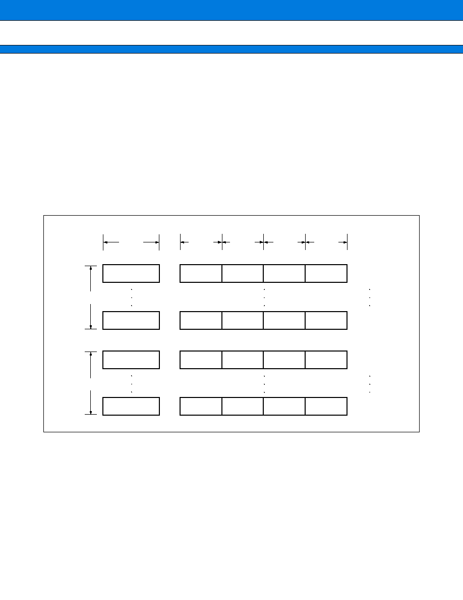
MB91301/MB91V301
47
s
INSTRUCTION CACHE
The instruction cache is a fast local memory for temporary storage. Once an instruction code is accessed from
external slower memory, the instruction cache holds the instruction code inside to increase the speed of access-
ing the same code from then on.
By setting the RAM mode, the instruction cache data RAM is made directly read/write-accessible by software.
∑
Configuration
∑ FR family's basic instruction length : Two bytes
∑ Block layout : Two-way set associative
∑ Blocks : 128 blocks per way
16 bytes per block (
=
4 sub-blocks)
4 bytes per sub-block (
=
1 bus access unit)
∑
Instruction Cache Configuration
4 bytes
4 bytes
4 bytes
4 bytes
4 bytes
I3
I2
I1
I0
Way 1
Way 2
128 block
128
block
Cash tag
Cash tag
Cash tag
Cash tag
Sub
block 3
Sub
block 3
Sub
block 2
Sub
block 1
Sub
block 0
Sub
block 3
Sub
block 2
Sub
block 1
Sub
block 0
Sub
block 3
Sub
block 2
Sub
block 1
Sub
block 0
block 0
block 0
block 127
block 127
Sub
block 2
Sub
block 1
Sub
block 0
MB91301/MB91V301
48
∑
Instruction Cache Tags
[bit 31 to bit 9] Address tag
The address tag stores the upper 23 bits of the memory address of the instruction cached in the corresponding
block.
For example, memory address IA of the instruction data stored in sub-block k in block i is obtained from the
following equation:
IA
=
address tag
◊
2
9
+
i
◊
2
4
+
k
◊
2
2
The address tag is used to check for a match with the instruction address requested for access by the CPU.
The CPU and cache behave as follows depending on the result of the tag check:
∑ When the requested instruction data exists in the cache (hit), the cache transfers the data to the CPU within
the cycle.
∑ When the requested instruction data does not exist in the cache (miss), the CPU and cache obtain the data
loaded by external access at the same time.
[bit 7 to bit4] SBV3 to SBV0 : Sub-block validation
When SBV
n
contains "1", the corresponding sub-block holds the current instruction data at the address located
by the tag. Each sub-block usually holds two instructions (excluding immediate-value transfer instructions).
[bit 3] TAGV : Tag validation bit
This bit indicates whether the address tag value is valid. When the bit contains "0", the corresponding block is
invalid regardless of the settings of the sub-block validation bits. (The bit is set to "0" when the cache is flushed.)
[bit 1] LRU (only in way 1)
This bit exists only in the instruction cache tag in way 1. The bit indicates way 1 or 2 as the way containing the
last entry accessed in the selected set. When set to "1", the LRU bit indicates that the entry of the set in way 1
is the last entry accessed. When set to "0", it indicates that the one in way 2 is the last entry accessed.
[bit 0] ETLK : Entry lock
This bit is used to lock all the entries in the block corresponding to the tag in the cache. When the ETLK bit is
set to "1", the entries are locked and are not updated when a cache miss occurs. Note, however, that invalid
sub-blocks are updated. If a cache miss occurs with both of ways 1 and 2 in the entry lock states, access to
external memory takes place after losing one cycle used for evaluating the cache miss.
07
06
05
04
03
02
01
00
SBV2
SBV3
SBV1
SBV0
TAGV
LRU
ETLK
31
09
08
07
06
05
04
03
02
01
00
SBV2
SBV3
SBV1
SBV0
TAGV
ETLK
31
09
08
Address tag
Way 1
Way 2
Address tag
Vacancy
Vacancy
Vacancy
Vacancy
MB91301/MB91V301
49
Control Registers
∑
Cache Size Register (ISIZE)
∑
Instruction Cache Control Register (ICHCR)
The instruction cache (I-cache) control register (ICHCR) controls the operations of the instruction cache.
Writing a value to the ICHCR has no effect on the caching of any instruction fetched within three cycles that follow.
bit
Initial value
Address : 00000307
H
- - - - - - 10
B
7
6
5
4
3
2
1
0
R/W
SIZE1
R/W
SIZE0
bit
Initial value
Address : 000003E7
H
0 - 000000
B
7
6
5
4
3
2
1
0
R/W
RAM
GBLK
ALFL
EOLK
ELKR
FLSH
R/W
R/W
R/W
R/W
R/W
R/W
ENAB
Address
00010000
H
00010200
H
00010400
H
00010600
H
00010800
H
00010FFF
H
TAG RAM
00010000
H
00010004
H
00010008
H
0001000C
H
00010010
H
00010014
H
00014000
H
00014200
H
00014400
H
00014600
H
00014800
H
00014FFF
H
00018000
H
00018200
H
00018400
H
00018600
H
00018800
H
00018FFF
H
0001C000
H
0001C200
H
0001C400
H
0001C600
H
0001C800
H
0001CFFF
H
Cache RAM
00018000
H
00018004
H
00018008
H
0001800C
H
00018010
H
00018014
H
Cache off
RAM off
Cache off
RAM on
TAG1
TAG2
IRAM1
$RAM1
IRAM2
$RAM2
<TAG1>
<TAG2>
<IRAM1>
<$RAM1>
<IRAM2>
IRAM1
IRAM2
IRAM1
IRAM2
<IRAM1>
<IRAM2>
IRAM1
IRAM2
<IRAM1>
<IRAM2>
<$RAM2>
TAG1
TAG2
$RAM1
$RAM2
<TAG1>
<TAG2>
<$RAM1>
<$RAM2>
TAG1
TAG2
$RAM1
$RAM2
<TAG1>
<TAG2>
<TAG1>
<TAG2>
<$RAM1>
<$RAM2>
IRAM1
IRAM2
TAG1
TAG2
$RAM1
$RAM2
<TAG1>
<TAG2>
<TAG1>
<TAG2>
<TAG1>
<TAG2>
<TAG1>
<TAG2>
<$RAM1>
<$RAM2>
Cache 4 K
RAM off
Cache 4 K
RAM on
Cache 2 K
RAM off
Cache 2 K
RAM on
Cache 1 K
RAM off
Cache
RAM on
TAG1
TAG RAM (way1)
TAG2
TAG RAM (way2)
<>
Mirror area
RAM on/off
RAM bit
=
I/O
$RAM1
Cahce RAM (way1) IRAM1
I-Bus RAM (way1)
$RAM2
Cahce RAM (way2) IRAM1
I-Bus RAM (way2)
Entry at address 00x
Mirror of 00x
Entry at address 00x
Mirror of 00x
Instruction at address 000 (SBV0)
Instruction at address 004 (SBV1)
Instruction at address 008 (SBV2)
Instruction at address 00C (SBV3)
Instruction at address 010 (SBV0)
Instruction at address 014 (SBV1)
MB91301/MB91V301
50
Address
Cache 4 K
Cache 2 K
Cache 1 K
Cache off
$RAM1
$RAM1
IRAM1
$RAM2
IRAM2
$RAM1
IRAM1
$RAM2
IRAM2
IRAM1
$RAM2
IRAM2
000
H
200
H
400
H
600
H
000
H
200
H
400
H
600
H
Address
00000000
H
00010000
H
00020000
H
00030000
H
00040000
H
00100000
H
FFFFFFFF
H
IRAM
IRAM
ROMA
=
0
(ROM absent)
ROMA
=
1
(ROM present)
Direct area
Direct area
Cache area
Cache area
Internal ROM
(Even the D-bus RAM area is cached if the
entry is on the instruction bus.)
Each chip-select area can be set as a non-
cache area.

MB91301/MB91V301
51
s
PERIPHERAL RESOURCES
1.
External Bus Interface Controller
∑
∑
∑
∑
External Bus Interface Controller Features
∑ Maximum output address width = 32-bit (4 GB memory space)
∑ Various different types of external memory (8-bit, 16-bit, or 32-bit devices) can be directly connected and the
controller can support multiple devices with different access timings.
Asynchronous SRAM, asynchronous ROM/FLASH memory (supports multiple write strobe access or byte-
enable access)
Page mode ROM/FLASH memory (2, 4, or 8 page size)
Burst mode ROM/FLASH memory
Address/data multiplexed bus (8-bit or 16-bit width only)
Synchronous memory (built-in ASIC memory, etc.)
Note:
Synchronous SRAM cannot be directly connected.
∑ Memory can be divided into eight independent banks (chip select areas) with a separate chip select output
for each bank.
The size of each area can be set in 64 Kbyte increments (the size of each chip select area can range from
64 Kbyte to 2 Gbyte)
Each area can be located anywhere in the physical address space (subject to boundary limitations based on
the area size)
∑ The following functions can be set independently for each chip select area :
Chip select area enable/disable (Access is not performed to disabled areas)
Setting of an access timing type to support each type of memory (For SDRAM, only the CS6 and CS7 areas
can be connected.)
Detailed access timing settings (wait cycles and similar settings for each access type)
Data bus width (8-bit, 16-bit, 32-bit)
Byte-ordering setting (big or little endian)
Note:
The CS0 area must be big endian.
Write-prohibit setting (read-only areas)
Enable or disable loading into built-in cache
Enable or disable prefetch function
Maximum burst length setting (1, 2, 4, 8)
∑ Different detailed timing settings can be set for each timing type
Even for the same type, different settings can be used for each chip select area.
Up to 15 auto-wait cycles can be specified. (For asynchronous SRAM, ROM, Flash, and I/O areas)
The bus cycle can be extended by the external RDY input. (For asynchronous SRAM, ROM, Flash, and I/O
areas)
Fast access wait and page wait settings are supported (For burst/page mode ROM and Flash areas)
Idle cycles, recovery cycles, setup delays, and similar can be inserted.
Capable of setting timing values such as the CAS latency and RAS-CAS delay (SDRAM area)
Capable of controlling the distributed/centralized auto-refresh, self-refresh, and other refresh timings (SDRAM
area)
∑ DMA supports fly-by transfer
Transfer between memory and I/O can be performed by a single access.
Memory wait cycles can be synchronized with the I/O wait period during fly-by transfer.
Hold times can be maintained by extending access to the data source only.
Separate idle and recovery cycle settings can be specified for use in fly-by transfer.
∑ Supports external bus arbitration using BRQ and BGRNT.
∑ Pins not used by the external interface can be set as general purpose I/O ports.
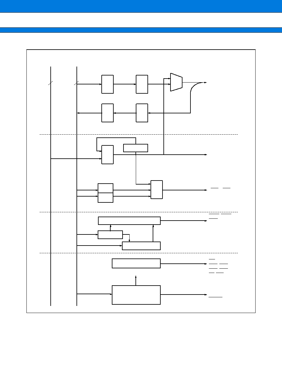
MB91301/MB91V301
52
∑
Block Diagram
MUX
CS0 to CS7
RD
WR0, WR1,
WR2, WR3,
AS, BAA
SRAS, SCAS,
SWE, MCLKE,
DQMUU, DQMUL,
DQMLU, DQMLL
BRQ
BGRNT
RDY
32
32
write buffer
read buffer
switch
switch
+
1 or
+
2
address buffer
ASR
ASZ
comparator
DATA BLOCK
ADDRESS BLOCK
registers
&
control
SDRAM control
RCR
under flow
refresh counter
External pin controller
All block control
Internal
address bus
Internal
data bus
External data bus
External address
bus
MB91301/MB91V301
53
∑
I/O pin
External interface pin (Some pins are general purpose pins.)
The following shows I/O pins of each interface.
∑ Normal bus interface
A23 to A00, D31 to D00 (AD15 to AD00)
CS0, CS1, CS2, CS3, CS4, CS5, CS6, CS7
AS, SYSCLK, MCLK,
RD
WR, WR0 (UUB) , WR1 (ULB) , WR2 (ULB) , WR3 (LLB) ,
RDY, BRQ, BGRNT
∑ Memory interface
MCLK, MCLKE
MCLKI (for SDRAM)
LBA (
=
AS) , BAA (for burst ROM/FLASH)
SRAS, SCAS, SWE (
=
WR) (for SDRAM)
DQMUU, DQMUL, DQMLU, DQMLL (for SDRAM (
=
WR0, WR1, WR2, WR3) )
∑ DMA interface
IOWR, IORD
DACK0, DACK1
DREQ0, DREQ1
DEOP0, DEOP1
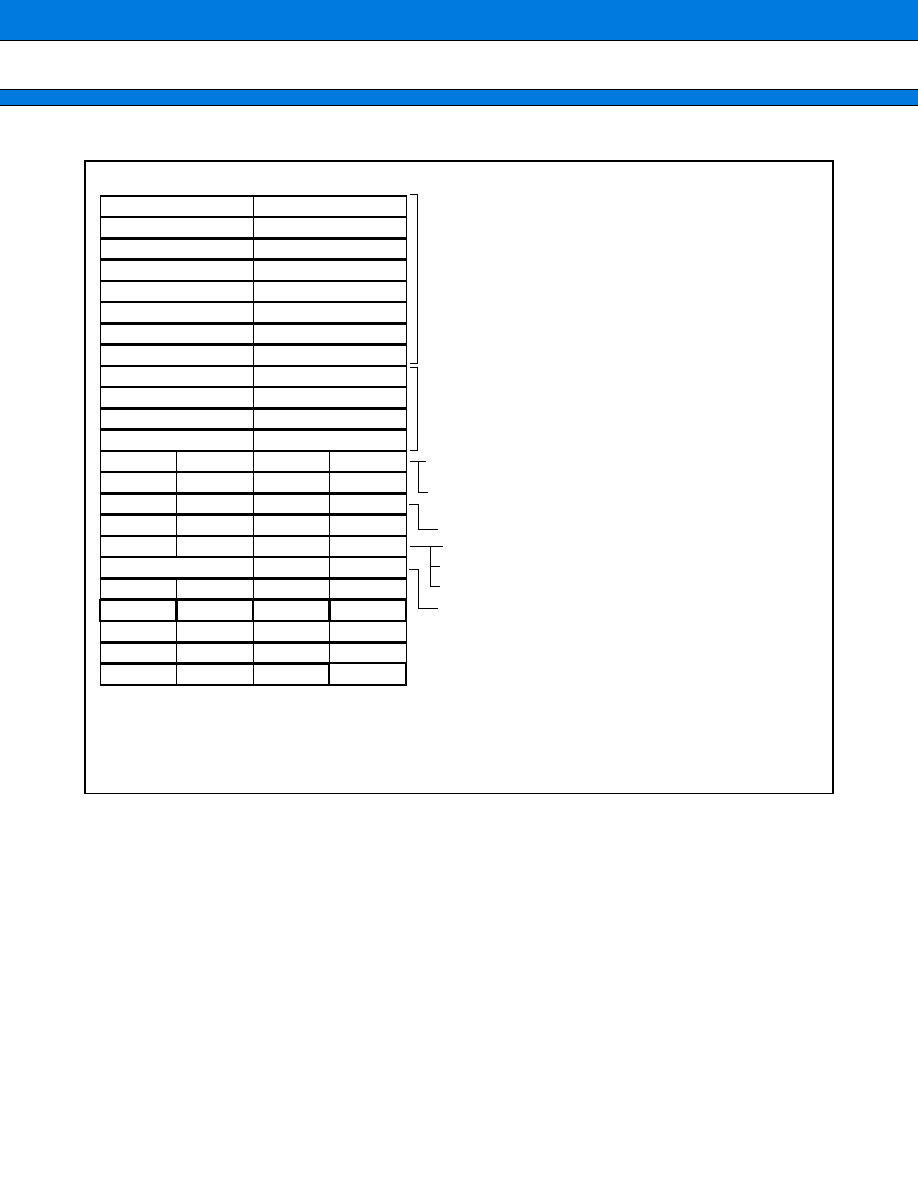
MB91301/MB91V301
54
∑
Register List
31
23
24
15
16
07
08
00
ASR0
ACR0
ASR1
ACR1
ASR2
ACR2
ASR3
ACR3
ASR4
ACR4
ASR5
ACR5
ASR6
ACR6
ASR7
ACR7
AWR0
AWR1
AWR2
AWR3
AWR4
AWR5
AWR6
RCR
MCRA
MCRB
IOWR0
IOWR1
CSER
CHER
TCR
(MODR)
AWR7
Reserved
Reserved
Reserved
Reserved
Reserved
Reserved
Reserved
Reserved
Reserved
Reserved
Reserved
Reserved
Reserved
Reserved
Reserved
Reserved
Reserved
Reserved
Reserved
Reserved
Reserved
Reserved
Reserved
Reserved
Reserved
Reserved
Reserved
Reserved
Reserved
Reserved
Reserved
Reserved
Reserved
Reserved
Notes :
∑
Reserved indicates a reserved register. When writing, always set to "0".
∑
The MODR register cannot be accessed by the user program.
Area select registers 0 to 7 (ASR0 to ASR7)
Area configuration registers 0 to 7 (ACR0 to ACR7)
Area weight register (AWR0 to AWR7)
Memory setting register
(For SDRAM/FCRAM auto-precharge OFF mode) (MCRA)
Memory setting register
(For FCRAM auto-precharge ON mode) (MCRB)
DMAC I/O wait registers (IOWR0 and IOWR1)
Chip-select area enable register (CSER)
Cache fetch enable register (CHER)
Terminal and timing control register (TCR)
Refresh control register (RCR)
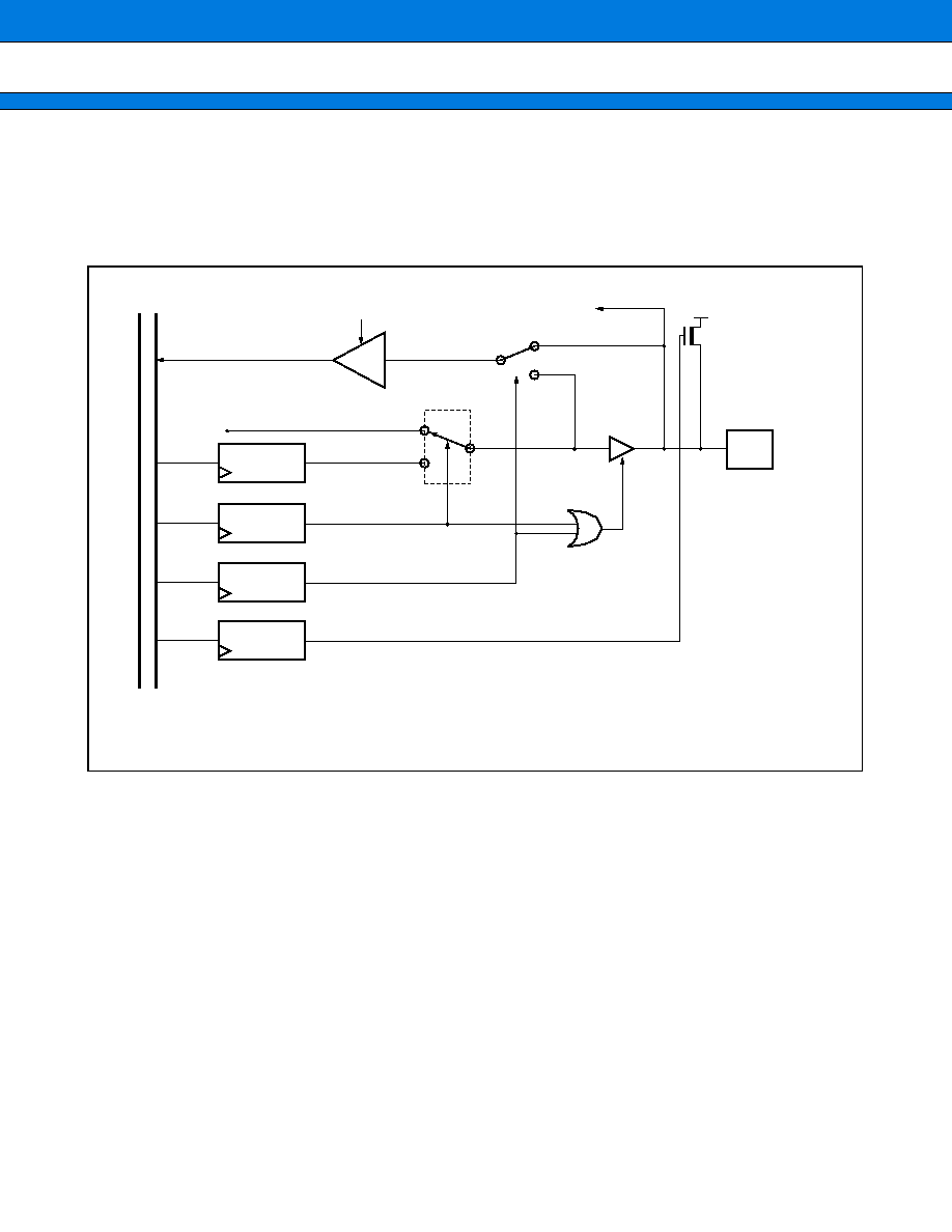
MB91301/MB91V301
55
2.
I/O Ports
MB91301/MB91V301 pins can be used as I/O ports when not set for use by the external bus interface or the
various peripheral I/O functions.
∑
I/O port (with pull-up resistor) block diagram
Note : For port output, the pull-up resistor is disabled irrespective of the setting.
I/O ports with pull-up resistors have the following registers :
∑
PDR (Port Data Register)
∑
DDR (Data Direction Register)
∑
PFR (Port Function Register)
∑
PCR (Pull-up Control Register)
I/O ports have three following modes
∑ When port is in input mode (PFR
=
"0" & DDR
=
"0")
PDR read : Reads the level of the corresponding external pin.
PDR write : Writes the value to the PDR.
∑ When port is in output mode (PFR
=
"0" & DDR
=
"1")
PDR read : Reads the PDR value.
PDR write : Outputs the PDR value to the corresponding external pin.
∑ When port is in peripheral output mode (PFR
=
"1" & DDR
=
"X")
PDR
: Reads the value of the corresponding peripheral output.
PDR write : Writes the value to the PDR.
Port Bus
0
1
1
0
Pin
PDR
PFR
DDR
PCR
PDR
DDR
PFR
PCR
: Port Data Register
: Data Direction Register
: Port Function Register
: Pull-up Control Register
Peripheral output
PDR read
Peripheral input
Pull-up resistor
(approx. 25 k
)
PCR
=
0 : No pull-up resistor
PCR
=
1 : Use pull-up resistor

MB91301/MB91V301
56
Notes :
∑
Use byte access to access ports.
∑
The external bus function has priority for port 0 to port A when these are used as external bus pins.
Accordingly, writing to the DDR has no effect on the pin input/output setting while the pins are operating
as external bus pins. The value set in the DDR becomes meaningful when the PFR register is modified
to set the pins as general purpose ports.
∑
In stop mode (HIZ = 0), the pull-up resistor control register setting is used.
∑
In stop mode (HIZ = 1), the pull-up resistor control register setting is ignored during hardware standby.
∑
Using pull-up resistors is prohibited when these pins are used as external bus pins. In this case, do not
write '1" to the corresponding bit in the pull-up control register (PCR).
MB91301/MB91V301
57
∑
Port Data Register (PDR)
∑
PDR0 to PDR2, PDR6, PDR8 to PDRB, PDRG, PDRH and PDRJ are the I/O data registers for the I/O pots.
∑
The corresponding PDR0 to DDRJ and PFR6 to PFRJ registers control input/output.
∑
P00 to P07, P10 to P17 and P20 to P27 do not have a PFR (port function register).
PDR0
Initial value
Address : 00000000
H
XXXXXXXX
B
PDR1
Initial value
Address : 00000001
H
XXXXXXXX
B
PDR2
Initial value
Address : 00000002
H
XXXXXXXX
B
PDR6
Initial value
Address : 00000006
H
XXXXXXXX
B
PDR8
Initial value
Address : 00000008
H
XXXXXXXX
B
PDR9
Initial value
Address : 00000009
H
- XXXXXXX
B
PDRA
Initial value
Address : 0000000A
H
XXXXXXXX
B
PDRB
Initial value
Address : 0000000B
H
XXXXXXXX
B
PDRG
Initial value
Address : 00000010
H
XXXXXXXX
B
PDRH
Initial value
Address : 00000011
H
- - - - - XXX
B
PDRJ
Initial value
Address : 00000013
H
XXXXXXXX
B
R/W
R/W
R/W
R/W
R/W
R/W
R/W
R/W
7
6
5
4
3
2
1
0
P06
P07
P05
P04
P03
P02
P01
P00
7
6
5
4
3
2
1
0
P16
P17
P15
P14
P13
P12
P11
P10
R/W
R/W
R/W
R/W
R/W
R/W
R/W
R/W
7
6
5
4
3
2
1
0
P26
P27
P25
P24
P23
P22
P21
P20
R/W
R/W
R/W
R/W
R/W
R/W
R/W
R/W
7
6
5
4
3
2
1
0
P66
P67
P65
P64
P63
P62
P61
P60
R/W
R/W
R/W
R/W
R/W
R/W
R/W
R/W
7
6
5
4
3
2
1
0
P86
P87
P85
P84
P83
P82
P81
P80
R/W
R/W
R/W
R/W
R/W
R/W
R/W
R/W
7
6
5
4
3
2
1
0
P96
P95
P94
P93
P92
P91
P90
R/W
R/W
R/W
R/W
R/W
R/W
R/W
R/W
7
6
5
4
3
2
1
0
PA6
PA7
PA5
PA4
PA3
PA2
PA1
PA0
R/W
R/W
R/W
R/W
R/W
R/W
R/W
R/W
7
6
5
4
3
2
1
0
PB6
PB7
PB5
PB4
PB3
PB2
PB1
PB0
R/W
R/W
R/W
R/W
R/W
R/W
R/W
R/W
7
6
5
4
3
2
1
0
PG6
PG7
PG5
PG4
PG3
PG2
PG1
PG0
R/W
R/W
R/W
R/W
R/W
R/W
R/W
R/W
7
6
5
4
3
2
1
0
PH2
PH1
PH0
R/W
R/W
R/W
R/W
R/W
R/W
R/W
R/W
7
6
5
4
3
2
1
0
PJ6
PJ7
PJ5
PJ4
PJ3
PJ2
PJ1
PJ0
R/W
R/W
R/W
R/W
R/W
R/W
R/W
R/W
MB91301/MB91V301
58
∑
Data Direction Register (DDR)
DDR0 to DDR2, DDR6, DDR8 to DDRB, DDRG, DDRH and DDRJ control the direction (input or output) of each
bit in the corresponding port.
When PFR
=
0 DDR
=
0 : Port input
DDR
=
1 : Port output
When PFR
=
1 DDR
=
0 : Peripheral input
DDR
=
1 : Peripheral output
DDR0
Initial value
Address : 00000600
H
00000000
B
DDR1
Initial value
Address : 00000601
H
00000000
B
DDR2
Initial value
Address : 00000602
H
00000000
B
DDR6
Initial value
Address : 00000606
H
00000000
B
DDR8
Initial value
Address : 00000608
H
00000000
B
DDR9
Initial value
Address : 00000609
H
- 0000000
B
DDRA
Initial value
Address : 0000060A
H
00000000
B
DDRB
Initial value
Address : 0000060B
H
00000000
B
DDRG
Initial value
Address : 00000400
H
00000000
B
DDRH
Initial value
Address : 00000401
H
- - - - - 000
B
DDRJ
Initial value
Address : 00000403
H
00000000
B
R/W
R/W
R/W
R/W
R/W
R/W
R/W
R/W
7
6
5
4
3
2
1
0
P06
P07
P05
P04
P03
P02
P01
P00
7
6
5
4
3
2
1
0
P16
P17
P15
P14
P13
P12
P11
P10
R/W
R/W
R/W
R/W
R/W
R/W
R/W
R/W
7
6
5
4
3
2
1
0
P26
P27
P25
P24
P23
P22
P21
P20
R/W
R/W
R/W
R/W
R/W
R/W
R/W
R/W
7
6
5
4
3
2
1
0
P66
P67
P65
P64
P63
P62
P61
P60
R/W
R/W
R/W
R/W
R/W
R/W
R/W
R/W
7
6
5
4
3
2
1
0
P86
P87
P85
P84
P83
P82
P81
P80
R/W
R/W
R/W
R/W
R/W
R/W
R/W
R/W
7
6
5
4
3
2
1
0
P96
P95
P94
P93
P92
P91
P90
R/W
R/W
R/W
R/W
R/W
R/W
R/W
R/W
7
6
5
4
3
2
1
0
PA6
PA7
PA5
PA4
PA3
PA2
PA1
PA0
R/W
R/W
R/W
R/W
R/W
R/W
R/W
R/W
7
6
5
4
3
2
1
0
PB6
PB7
PB5
PB4
PB3
PB2
PB1
PB0
R/W
R/W
R/W
R/W
R/W
R/W
R/W
R/W
7
6
5
4
3
2
1
0
PG6
PG7
PG5
PG4
PG3
PG2
PG1
PG0
R/W
R/W
R/W
R/W
R/W
R/W
R/W
R/W
7
6
5
4
3
2
1
0
PH2
PH1
PH0
R/W
R/W
R/W
R/W
R/W
R/W
R/W
R/W
7
6
5
4
3
2
1
0
PJ6
PJ7
PJ5
PJ4
PJ3
PJ2
PJ1
PJ0
R/W
R/W
R/W
R/W
R/W
R/W
R/W
R/W
MB91301/MB91V301
59
∑
Pull-up Resistor Control Register (PCR)
PCR0 to PCR2, PCR6, PCR8 to PCRB, PCRG, PCRH and PCRJ control the pull-up resistors for the corre-
sponding port.
PCR
=
0 : No pull-up resistor
PCR
=
1 : Use pull-up resistor
PCR0
bit
Initial value
Address :
00000620
H
00000000
B
PCR1
bit
Initial value
Address :
00000621
H
00000000
B
PCR2
bit
Initial value
Address :
00000622
H
00000000
B
PCR6
bit
Initial value
Address :
00000626
H
00000000
B
PCR8
bit
Initial value
Address :
00000628
H
00000000
B
PCR9
bit
Initial value
Address :
00000629
H
- 000 - - 0 -
B
PCRA
bit
Initial value
Address :
0000062A
H
00000000
B
PCRB
bit
Initial value
Address :
0000062B
H
00000000
B
PCRG
bit
Initial value
Address :
00000420
H
00000000
B
PCRH
bit
Initial value
Address :
00000421
H
- - - - - 000
B
PCRJ
bit
Initial value
Address :
00000423
H
00000000
B
R/W
R/W
R/W
R/W
R/W
R/W
R/W
R/W
7
6
5
4
3
2
1
0
P06
P07
P05
P04
P03
P02
P01
P00
7
6
5
4
3
2
1
0
P16
P17
P15
P14
P13
P12
P11
P10
R/W
R/W
R/W
R/W
R/W
R/W
R/W
R/W
7
6
5
4
3
2
1
0
P26
P27
P25
P24
P23
P22
P21
P20
R/W
R/W
R/W
R/W
R/W
R/W
R/W
R/W
7
6
5
4
3
2
1
0
P66
P67
P65
P64
P63
P62
P61
P60
R/W
R/W
R/W
R/W
R/W
R/W
R/W
R/W
7
6
5
4
3
2
1
0
P86
P87
P85
P84
P83
P82
P81
P80
R/W
R/W
R/W
R/W
R/W
R/W
R/W
R/W
7
6
5
4
3
2
1
0
P96
P95
P94
P91
R/W
R/W
R/W
R/W
R/W
R/W
R/W
R/W
7
6
5
4
3
2
1
0
PA6
PA7
PA5
PA4
PA3
PA2
PA1
PA0
R/W
R/W
R/W
R/W
R/W
R/W
R/W
R/W
7
6
5
4
3
2
1
0
PB6
PB7
PB5
PB4
PB3
PB2
PB1
PB0
R/W
R/W
R/W
R/W
R/W
R/W
R/W
R/W
7
6
5
4
3
2
1
0
PG6
PG7
PG5
PG4
PG3
PG2
PG1
PG0
R/W
R/W
R/W
R/W
R/W
R/W
R/W
R/W
7
6
5
4
3
2
1
0
PH2
PH1
PH0
R/W
R/W
R/W
R/W
R/W
R/W
R/W
R/W
7
6
5
4
3
2
1
0
PJ6
PJ7
PJ5
PJ4
PJ3
PJ2
PJ1
PJ0
R/W
R/W
R/W
R/W
R/W
R/W
R/W
R/W
MB91301/MB91V301
60
∑ Port Function Register (PFR)
PFR6, PFR8 to PFRB, PFRA2, PFRG, PFRH and PFRJ control the output for the corresponding external bus
interface or peripheral output bit.
Always write "0" to unused bits in the PFR.
PFR6
bit
Initial value
Address :
00000616
H
11111111
B
PFR8
bit
Initial value
Address :
00000618
H
111 - - 0 - -
B
PFR9
bit
Initial value
Address :
00000619
H
- 0000111
B
PFRA1
bit
Initial value
Address :
0000061A
H
11111111
B
PFRB1
bit
Initial value
Address :
0000061B
H
00000000
B
PFRB2
bit
Initial value
Address :
0000061C
H
0000 - - 00
B
PFRA2
bit
Initial value
Address :
0000061E
H
- 0 - - - - - -
B
PFRG
bit
Initial value
Address :
00000410
H
00 - - - - - -
B
PFRH
bit
Initial value
Address :
00000411
H
- - - - - - 0 -
B
PFRJ
bit
Initial value
Address :
00000413
H
- 000 - 00 -
B
7
6
5
4
3
2
1
0
A22E
A23E
A21E
A20E
A19E
A18E
A17E
A16E
R/W
R/W
R/W
R/W
R/W
R/W
R/W
R/W
7
6
5
4
3
2
1
0
WR2XE
WR3XE
WR1XE
BRQE
R/W
R/W
R/W
R/W
R/W
R/W
R/W
R/W
7
6
5
4
3
2
1
0
WRXE
BAAE
ASXE
MCKE
MCKEE
SYSE
R/W
R/W
R/W
R/W
R/W
R/W
R/W
R/W
7
6
5
4
3
2
1
0
CS6XE
CS7XE
CS5XE
CS4XE
CS3XE
CS2XE
CS1XE
CS0XE
R/W
R/W
R/W
R/W
R/W
R/W
R/W
R/W
7
6
5
4
3
2
1
0
AK12
DES1
AK11
AK10
DES0
AK02
AK01
AK00
R/W
R/W
R/W
R/W
R/W
R/W
R/W
R/W
7
6
5
4
3
2
1
0
DWRE
DRDE
PPE1
AKH1
AKH0
R/W
R/W
R/W
R/W
R/W
R/W
R/W
R/W
7
6
5
4
3
2
1
0
PPE2
R/W
R/W
R/W
R/W
R/W
R/W
R/W
R/W
7
6
5
4
3
2
1
0
SOE2
SCE2
R/W
R/W
R/W
R/W
R/W
R/W
R/W
R/W
7
6
5
4
3
2
1
0
PPE3
R/W
R/W
R/W
R/W
R/W
R/W
R/W
R/W
7
6
5
4
3
2
1
0
PPE0
SCE1
SOE1
SCE0
SOE0
R/W
R/W
R/W
R/W
R/W
R/W
R/W
R/W
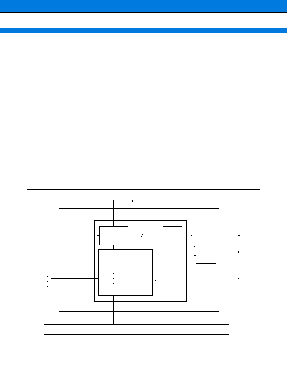
MB91301/MB91V301
61
3.
Interrupt Controller
The interrupt controller receives and processes interrupts.
∑
∑
∑
∑
Hardware Configuration
The interrupt controller consists of the following :
∑ ICR register
∑ Interrupt priority determination circuit
∑ Interrupt level and interrupt number (vector) generator
∑ Hold request removal request generator
∑
∑
∑
∑
Principal Functions
The main functions of the interrupt controller are as follows :
∑ Detect NMI and interrupt requests
∑ Prioritize interrupts (according to level and number)
∑ Notify interrupt level of selected interrupt request (to CPU)
∑ Notify interrupt number of selected interrupt request (to CPU)
If an NMI or interrupt request with an interrupt level other than "11111
B
" occurs, notify recovery from stop mode
(to CPU)
∑ Generate hold request removal requests to the bus master
∑
Block Diagram
RI00
RI47
(DLYIRQ)
5
6
LEVEL4 to
LEVEL0
MHALTI
VCT5 to
VCT0
R-BUS
UNMI
WAKEUP
ICR00
ICR47
("1" when LEVEL
11111
B
)
Determine order of priority
NMI
processing
LEVEL
determination
VECTOR
determination
LEVEL,
VECTOR
genera-
tion
HLDREQ
removal
request
MB91301/MB91V301
62
∑
Register List
(Continued)
Address :
Address :
Address :
Address :
Address :
Address :
Address :
Address :
Address :
Address :
Address :
Address :
Address :
Address :
Address :
Address :
Address :
Address :
Address :
Address :
Address :
Address :
Address :
Address :
Address :
Address :
Address :
Address :
Address :
Address :
Address :
Address :
7
bit
6
5
4
3
2
1
0
ICR4
ICR3
ICR2
ICR1
ICR0
ICR4
ICR3
ICR2
ICR1
ICR0
ICR4
ICR3
ICR2
ICR1
ICR0
ICR4
ICR3
ICR2
ICR1
ICR0
ICR4
ICR3
ICR2
ICR1
ICR0
ICR4
ICR3
ICR2
ICR1
ICR0
ICR4
ICR3
ICR2
ICR1
ICR0
ICR4
ICR3
ICR2
ICR1
ICR0
ICR4
ICR3
ICR2
ICR1
ICR0
ICR4
ICR3
ICR2
ICR1
ICR0
ICR4
ICR3
ICR2
ICR1
ICR0
ICR4
ICR3
ICR2
ICR1
ICR0
ICR4
ICR3
ICR2
ICR1
ICR0
ICR4
ICR3
ICR2
ICR1
ICR0
ICR4
ICR3
ICR2
ICR1
ICR0
ICR4
ICR3
ICR2
ICR1
ICR0
ICR4
ICR3
ICR2
ICR1
ICR0
ICR4
ICR3
ICR2
ICR1
ICR0
ICR4
ICR3
ICR2
ICR1
ICR0
ICR4
ICR3
ICR2
ICR1
ICR0
ICR4
ICR3
ICR2
ICR1
ICR0
ICR4
ICR3
ICR2
ICR1
ICR0
ICR4
ICR3
ICR2
ICR1
ICR0
ICR4
ICR3
ICR2
ICR1
ICR0
ICR4
ICR3
ICR2
ICR1
ICR0
ICR4
ICR3
ICR2
ICR1
ICR0
ICR4
ICR3
ICR2
ICR1
ICR0
ICR4
ICR3
ICR2
ICR1
ICR0
ICR4
ICR3
ICR2
ICR1
ICR0
ICR4
ICR3
ICR2
ICR1
ICR0
ICR4
ICR3
ICR2
ICR1
ICR0
ICR4
ICR3
ICR2
ICR1
ICR0
ICR00
ICR01
ICR02
ICR03
ICR04
ICR05
ICR06
ICR07
ICR08
ICR09
ICR10
ICR11
ICR12
ICR13
ICR14
ICR15
ICR16
ICR17
ICR18
ICR19
ICR20
ICR21
ICR22
ICR23
ICR24
ICR25
ICR26
ICR27
ICR28
ICR29
ICR30
ICR31
00000440
H
00000441
H
00000442
H
00000443
H
00000444
H
00000445
H
00000446
H
00000447
H
00000448
H
00000449
H
0000044A
H
0000044B
H
0000044C
H
0000044D
H
0000044E
H
0000044F
H
00000450
H
00000451
H
00000452
H
00000453
H
00000454
H
00000455
H
00000456
H
00000457
H
00000458
H
00000459
H
0000045A
H
0000045B
H
0000045C
H
0000045D
H
0000045E
H
0000045F
H
MB91301/MB91V301
63
(Continued)
Address :
Address :
Address :
Address :
Address :
Address :
Address :
Address :
Address :
Address :
Address :
Address :
Address :
Address :
Address :
Address :
Address :
7
bit
6
5
4
3
2
1
0
ICR4
ICR3
ICR2
ICR1
ICR0
ICR4
ICR3
ICR2
ICR1
ICR0
ICR4
ICR3
ICR2
ICR1
ICR0
ICR4
ICR3
ICR2
ICR1
ICR0
ICR4
ICR3
ICR2
ICR1
ICR0
ICR4
ICR3
ICR2
ICR1
ICR0
ICR4
ICR3
ICR2
ICR1
ICR0
ICR4
ICR3
ICR2
ICR1
ICR0
ICR4
ICR3
ICR2
ICR1
ICR0
ICR4
ICR3
ICR2
ICR1
ICR0
ICR4
ICR3
ICR2
ICR1
ICR0
ICR4
ICR3
ICR2
ICR1
ICR0
ICR4
ICR3
ICR2
ICR1
ICR0
ICR4
ICR3
ICR2
ICR1
ICR0
ICR4
ICR3
ICR2
ICR1
ICR0
ICR4
ICR3
ICR2
ICR1
ICR0
MHALTI
LVL4
LVL3
LVL2
LVL1
LVL0
ICR32
ICR33
ICR34
ICR35
ICR36
ICR37
ICR38
ICR39
ICR40
ICR41
ICR42
ICR43
ICR44
ICR45
ICR46
ICR47
HRCL
00000460
H
00000461
H
00000462
H
00000463
H
00000464
H
00000465
H
00000466
H
00000467
H
00000468
H
00000469
H
0000046A
H
0000046B
H
0000046C
H
0000046D
H
0000046E
H
0000046F
H
0000045
H
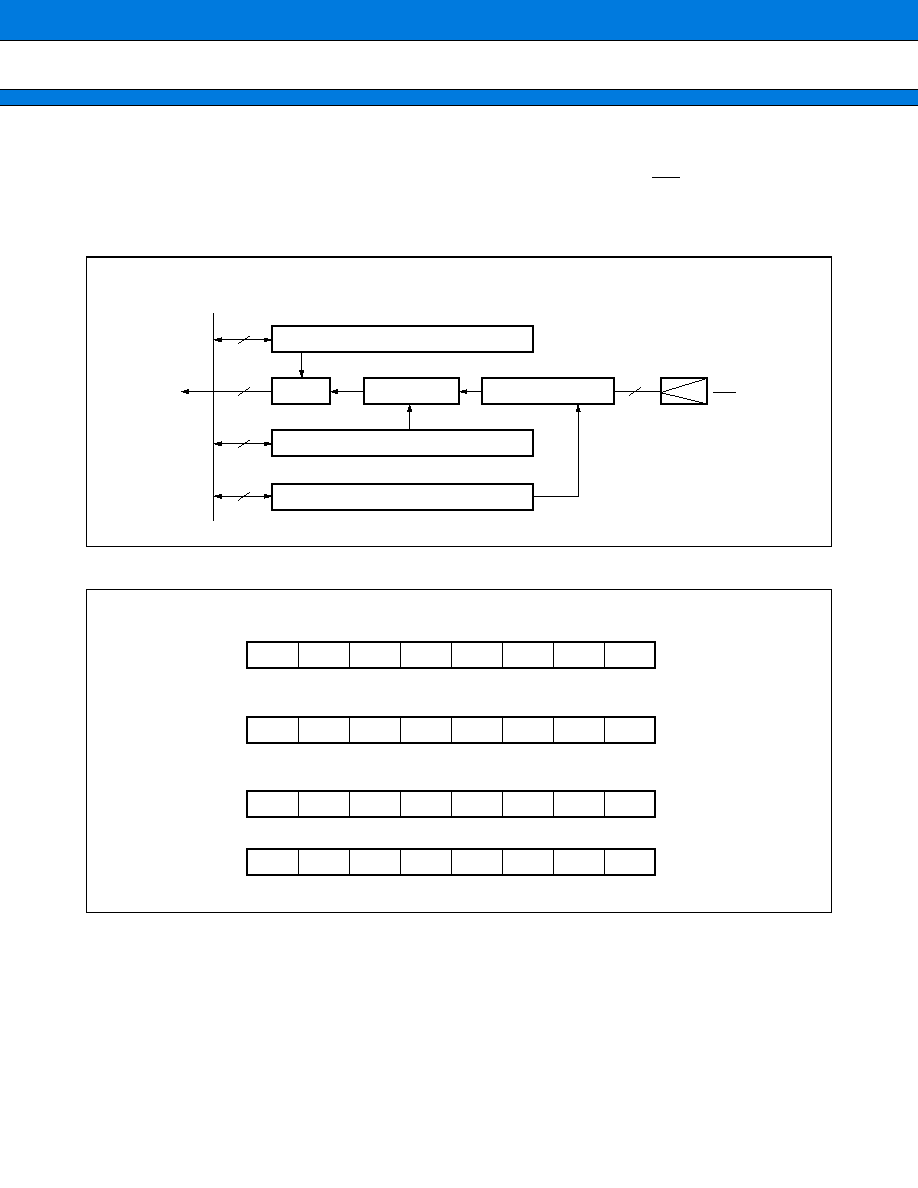
MB91301/MB91V301
64
4.
External Interrupt/NMI Control Block
The external interrupt control block controls external interrupt requests input to the NMI and INT0 to INT7 pins.
The interrupt trigger level can be selected from "H", "L", "rising edge", or "falling edge" (except for NMI).
∑
Block Diagram
∑
Register List
9
9
INT0 to INT7
NMI
8
8
8
R-BUS
Interrupt
request
Interrupt enable register
Gate
Request F/F
Edge detection circuit
Interrupt request register
Interrupt level setting register
External interrupt enable register (ENIR)
External interrupt request register (EIRR)
Request level setting register (ELVR)
bit
bit
bit
bit
7
6
5
4
3
2
1
0
EN6
EN7
EN5
EN4
EN3
EN2
EN1
EN0
15
14
13
12
11
10
9
8
ER6
ER7
ER5
ER4
ER3
ER2
ER1
ER0
15
14
13
12
11
10
9
8
LA7
LB7
LB6
LA6
LB5
LA5
LB4
LA4
7
6
5
4
3
2
1
0
LA3
LB3
LB2
LA2
LB1
LA1
LB0
LA0
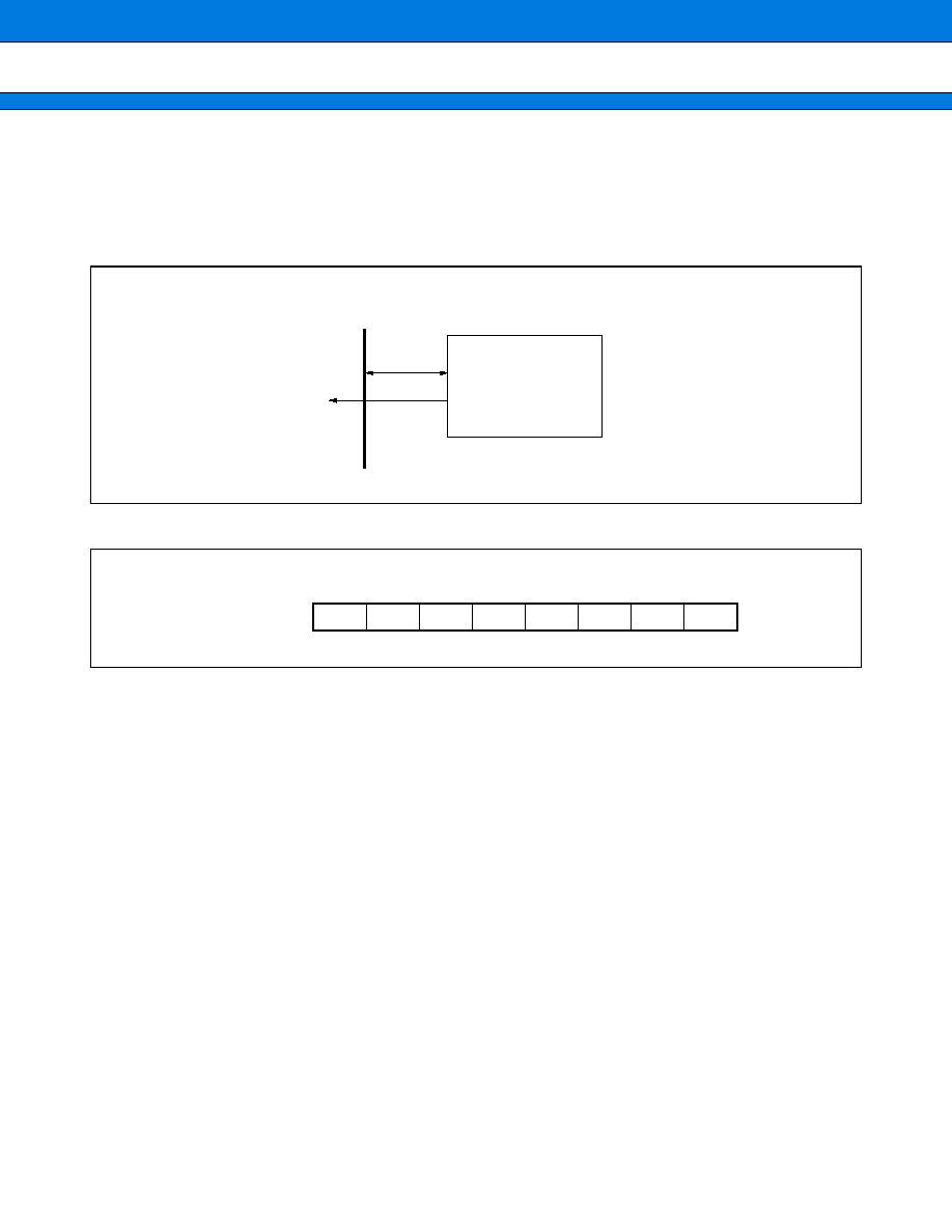
MB91301/MB91V301
65
5.
Delay Interrupt Module
The delay interrupt module is used to generate interrupts for task switching.
This module can be used to generate and cancel interrupts to the CPU via software.
∑
Block Diagram
∑
Register List
DLYI
R-bus
Interrupt request
Delay interrupt control register (DICR)
bit
7
6
5
4
3
2
1
0
DLYI

MB91301/MB91V301
66
6.
PPG Timer
The PPG timer can output highly precise PWM waveforms efficiently.
The MB91301/MB91V301 contains four channels of PPG timer.
∑
Features of the PPG Timer
∑ Each channel consists of a 16-bit down counter, a 16-bit data register with cycle setting buffer, a 16-bit compare
register with duty setting buffer, and pin control section.
∑ The count clocks for the 16-bit down counter can be selected from the following four types :
Internal clock
,
/4,
/16,
/64
∑ The counter is initialized to "FFFF
H
" at a reset or counter borrow.
∑ Each channel has a PPG output.
∑ Register outline
Cycle setting register: Reload data register with buffer
Duty setting register: Compare register with buffer
Transfer from the buffer takes place upon a counter borrow.
∑ Pin control overview
A duty match sets the pin control section to 1. (Preferential)
A counter borrow resets it to 0.
The output value fix mode is available, which can each output all "L" (or "H").
A polarity can also be specified.
∑ An interrupt request can be generated at a combination of the following events :
Activation of the PPG timer
Counter borrow (cycle match)
Duty match
Counter borrow (cycle match) or duty match
DMA transfer can be initiated by the above interrupt request.
∑ It is possible to set the simultaneous activation of two or more channels by means of software or another
interval timer.
Restarting during operation can also be set.
∑ The request level to be detected can be selected from among "rising edge", "falling edge", and "both edges".
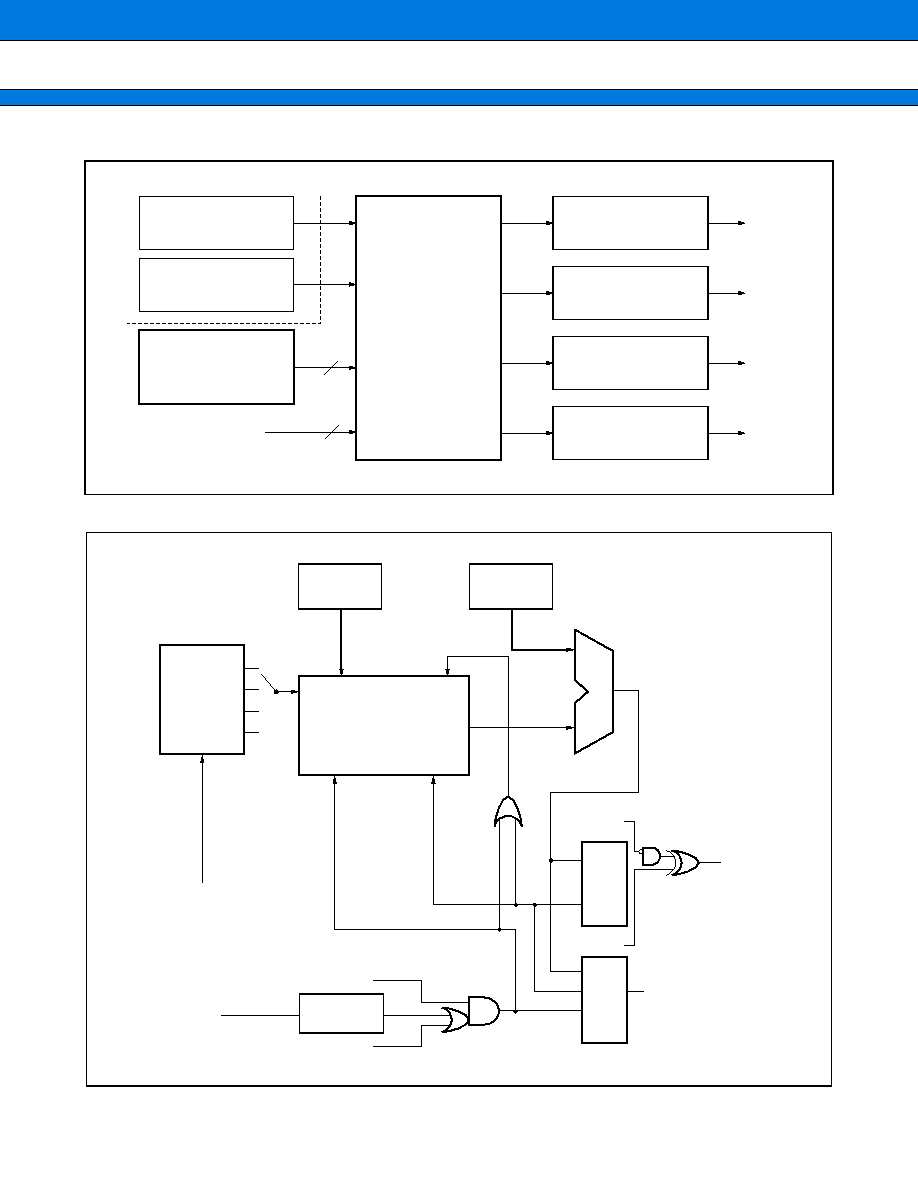
MB91301/MB91V301
67
∑
Block diagram
∑
Block diagram for 1 channel
4
4
PPG0
PPG1
PPG2
PPG3
16-bit reload timer
ch0
16
-
bit reload timer
ch1
General control
register 2
General
control
register 1
(resource select)
TRG input
PPG timer ch0
TRG input
PPG timer ch1
TRG input
PPG timer ch2
TRG input
PPG timer ch3
External TRG0 to TRG3
1 / 1
1 / 4
1 / 16
1 / 64
CK
PCRS
PDUT
cmp
S
R
Q
IRQ
Prescaler
16-bit down counter
Start
Borrow
Load
PPG mask
Conversion
bit
PPG output
Peripheral clock
TRG input
Edge
detection
Enable
Soft trigger
Interrupt
selection
MB91301/MB91V301
68
∑
Register List
GCN10
GCN20
PTMR0
PCSR0
PDUT0
PCNH0
PCNL0
PTMR1
PCSR1
PDUT1
PCNH1
PCNL1
PTMR2
PCSR2
PDUT2
PCNH2
15
7
bit
0
PCNL2
PTMR3
PCSR3
PDUT3
PCNH3
PCNL3
General control register 10
General control register 20
ch0 timer register
ch0 cycle setting register
ch0 duty setting register
ch0 control status register
ch1 timer register
ch1 cycle setting register
ch1 duty setting register
ch1 control status register
ch2 timer register
ch2 cycle setting register
ch2 duty setting register
ch2 control status register
ch3 timer register
ch3 cycle setting register
ch3
duty setting register
ch3 control status register
MB91301/MB91V301
69
7.
16-Bit Reload Timer
The 16-bit timer consists of a 16-bit down-counter, 16-bit reload register, prescaler for generating the internal
count clock, and a control register.
The clock source can be selected from three internal clock signals (machine clock divided by 2, 8, or 32) or the
external event.
The interrupt can be used to initiate DMA transfer.
The MB91301/MB91V301 has three 16-bit reload timer channels.
∑
Block Diagram
RELD
INTE
UF
CNTE
TRG
OUT
CTL.
CSL1
CSL0
MOD0
MOD1
MOD2
16
7
16
3
3
IN CTL.
2
2
2
1
3
5
3
EXCK
IRQ
R
|
B
U
S
16-bit reload register (TMRLR)
16-bit down counter (TMR) UF
Reload
Clock selector
Re-trigger
Prescaler
clear
External trigger input (TI)
External
trigger
selection
Count enable
CLKP input
MB91301/MB91V301
70
∑
Register List
Control status register (TMCSR)
16-bit timer register (TMR)
16-bit reload register (TMRLR)
bit
bit
bit
bit
15
14
13
12
11
10
9
8
CSL1
CSL0
MOD2
MOD1
7
6
5
4
3
2
1
0
MOD0
OUTL
RELD
INTE
UF
CNTE
TRG
15
0
15
0
MB91301/MB91V301
71
8.
U-TIMER (16 bit timer for UART baud rate generation)
The U-TIMER is a 16-bit timer used to generate the baud rate for the UART. Any desired baud rate can be set
using the combination of the chip operating frequency and U-TIMER reload value.
The U-TIMER can also be used as an interval timer by generating an interrupt from a count underflow event.
The MB91301/MB91V301 has three U-TIMER channels. When used as an interval timer, two U-TIMER channels
can be connected in cascade for a maximum count interval of up to 2
32
◊
.
Cascade connection is only available for channel 0 and channel 1 or channel 0 and channel 2.
∑
Block Diagram
UTIMR (reload register)
UTIM (timer)
clock
load
underflow
under flow U-TIMER 1
to UART
control
f.f.
15
15
0
0
MUX
Channel 0
only
(CLKP)
(Peripheral clock)
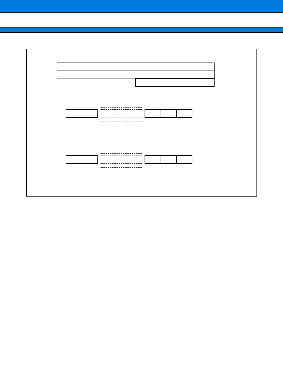
MB91301/MB91V301
72
∑
Register List
9.
UART
The UART is a serial I/O port for asynchronous (start-stop synchronized) or CLK synchronized transmission.
The MB91301/MB91V301 has three UART channels.
∑
∑
∑
∑
UART Features
∑ Full duplex double buffer
∑ Asynchronous (start-stop synchronized) or CLK synchronized transmission
∑ Supports multi-processor mode
∑ Fully programmable baud rate
The internal timer can be set to any desired baud rate (see "8. U-TIMER" description)
∑ Variable baud rate can be input from an external clock.
∑ Error detection functions (parity, framing, overrun)
∑ Transmission signal format is NRZ
∑ The interrupt can be used to initiate DMA transfer.
∑ The DMAC interrupt can be cleared by writing to the DRCL register.
∑ U-TIMER (UTIM)
UTIM contains the timer value. Use a 16-bit transfer instruction to access the register.
Reload register (UTIMR)
UTIMR is the register that contains the value to be reloaded to UTIM when UTIM causes an underflow.
Use a 16-bit transfer instruction to access the register.
Address
bit
Initial value
000064
H
(ch.0)
00006C
H
(ch.1)
000074
H
(ch.2)
00000000
00000000
B
Address
bit
Initial value
000064
H
(ch.0)
00006C
H
(ch.1)
000074
H
(ch.2)
00000000
00000000
B
UTIMR
UTIM
UTIMC
15
0
8 7
R
R
R
R
R
15
14
2
1
0
b14
b15
b2
b1
b0
W
W
W
W
W
15
14
2
1
0
b14
b15
b2
b1
b0
MB91301/MB91V301
73
∑
Block Diagram
MD1
MD0
CS0
SCKE
PEN
P
SBL
CL
A
/
D
REC
RXE
TXE
PE
ORE
FRE
RDRF
TDRE
BDS
RIE
TIE
R - BUS
SIDR
SODR
Control signal
From U-TIMER
External clock
SCK
Clock
selection
circuit
Receive status
decision circuit
Receive error
signal for DMA
(to DMAC)
RX clock
RX control circuit
Start bit detect
circuit
Receive bit
counter
Receive parity
counter
RX shifter
RX
complete
TX clock
RX interrupt
(to CPU)
TX interrupt
(to CPU)
TX control circuit
TX start
circuit
Send bit
counter
Send parity
counter
TX shifter
TX start
SMR
register
Control
signal
SCR
register
SSR
register
SCK (clock)
SI (Receive data)
SO (Send data)
MB91301/MB91V301
74
∑
Register List
Serial input data register
Serial output data register (SIDR/SODR)
Serial status register (SSR)
Serial mode register (SMR)
Serial control register (SCR)
DRCL register (DRCL)
bit
bit
bit
bit
bit
SIDR (R)/SODR (W)
SMR
SCR
(R/W)
(R/W)
(W)
SSR
DRCL
8 bit
8 bit
15
0
8 7
7
6
5
4
3
2
1
0
D6
D7
D5
D4
D3
D2
D1
D0
7
6
5
4
3
2
1
0
ORE
PE
FRE
RDRF
TDRE
BDS
RIE
TIE
7
6
5
4
3
2
1
0
MD0
MD1
CS0
SCKE
7
6
5
4
3
2
1
0
P
PEN
SBL
CL
A/D
REC
RXE
TXE
7
6
5
4
3
2
1
0

MB91301/MB91V301
75
10. A/D Converter (Successive Approximation Type)
The A/D converter converts analog input voltages to digital values.
∑
∑
∑
∑
A/D Converter Features
∑ Peripheral clock (CLKP) 140 clock cycle
∑ Minimum conversion time 4.1
µ
s/ch (for machine clock 34 MHz
=
CLKP)
∑ Built-in sample & hold circuit
∑ Resolution
=
10-bit
∑ 4 channel program-selectable analog inputs
Single conversion mode : Convert 1 specified channel
Scan conversion mode : Continuous conversion of multiple channels. Conversion can be specified for up
to 4 channels.
∑ Single, continuous, and stop conversion operation is supported.
Single conversion mode
: Convert specified channel then stop.
Continuous conversion mode : Perform continuous conversion for the selected channel.
Stop conversion mode
: Perform conversion for one channel, then wait for the next activation trigger
(synchronizes the conversion start timing)
∑ DMA transfer can be initiated by an interrupt.
∑ Selectable conversion activation trigger: Software, external trigger (falling edge), or reload timer (rising edge)
MB91301/MB91V301
76
∑
Block Diagram
∑
Register List
AV
CC
AN0
AN1
AN2
AN3
AVRH
AV
SS
AVR
R
|
B
U
S
Input switch
Sample & hold circuit
Channel decoder
Internal voltage
generator
Successive
approximation register
Data register
(ADCR : 10 bit)
A/D control register
(ADCS)
ATG (External pin trigger)
Reload timer ch2
(internal connection)
Timing generation circuit
Prescaler
Machine clock
(CLKP)
Data register
(ADCR0 to ADCR7 : 8
Upper 8 bit COPY
Control status register (ADCS)
Data register (ADCR)
Conversion result register (ADCR0 to ADCR3)
bit
bit
bit
bit
bit
15
14
13
12
11
10
9
8
INT
BUSY
INTE
CRF
STS1
STS0
STRT
7
6
5
4
3
2
1
0
MD0
MD1
ANS2
ANS1
ANS0
ANE2
ANE1
ANE0
15
14
13
12
11
10
9
8
9
8
7
6
5
4
3
2
1
0
6
7
5
4
3
2
1
0
7
6
5
4
3
2
1
0
6
7
5
4
3
2
1
0

MB91301/MB91V301
77
11. DMAC (DMA Controller)
The DMA controller is used to perform DMA (direct memory access) transfer on the FR series device.
Using DMA transfer under the control of the DMA controller improves system performance by enabling data to
be transferred at high speed independently of the CPU.
∑
∑
∑
∑
Hardware Configuration
∑ Independent DMA channels
◊
5 ch
∑ 5 ch independent access control circuits
∑ 32-bit address register (Supports reloading : 2 per channel)
∑ 16-bit transfer count register (Supports reloading : 1 per channel)
∑ 4-bit block count register (1 per channel)
∑ External transfer request input pins : DREQ0, DREQ1 (ch0, 1 only)
∑ External transfer request acknowledge output pins : DACK0, DACK1 (ch0, 1 only)
∑ DMA completion output pins : DEOP0, DEOP1 (ch0, 1 only)
∑ fly-by transfer (memory to I/O , I/O to memory) (ch0, 1 only)
∑ Two-cycle transfer
∑
∑
∑
∑
Main Functions of the DMA Controller
∑ Supports independent data transfer for multiple channels (5 channels)
(1) Priority order (ch.0
>
ch.1
>
ch.2
>
ch.3
>
ch.4)
(2) Order can be reversed for ch0 and ch1
(3) DMAC activation triggers
∑
Input from dedicated external pin (edge detection/level detection, ch0,1 only)
∑
Request from built-in peripheral (shared interrupt request, including external interrupts)
∑
Software request (register write)
(4) Transfer modes
∑
Demand transfer, burst transfer, step transfer, or block transfer
Addressing mode: Full 32-bit address (increment/decrement/fixed)
(address increment can be in the range
-
255 to
+
255)
∑
Data type : byte/half-word/word
∑
Single-shot or reload operation selectable
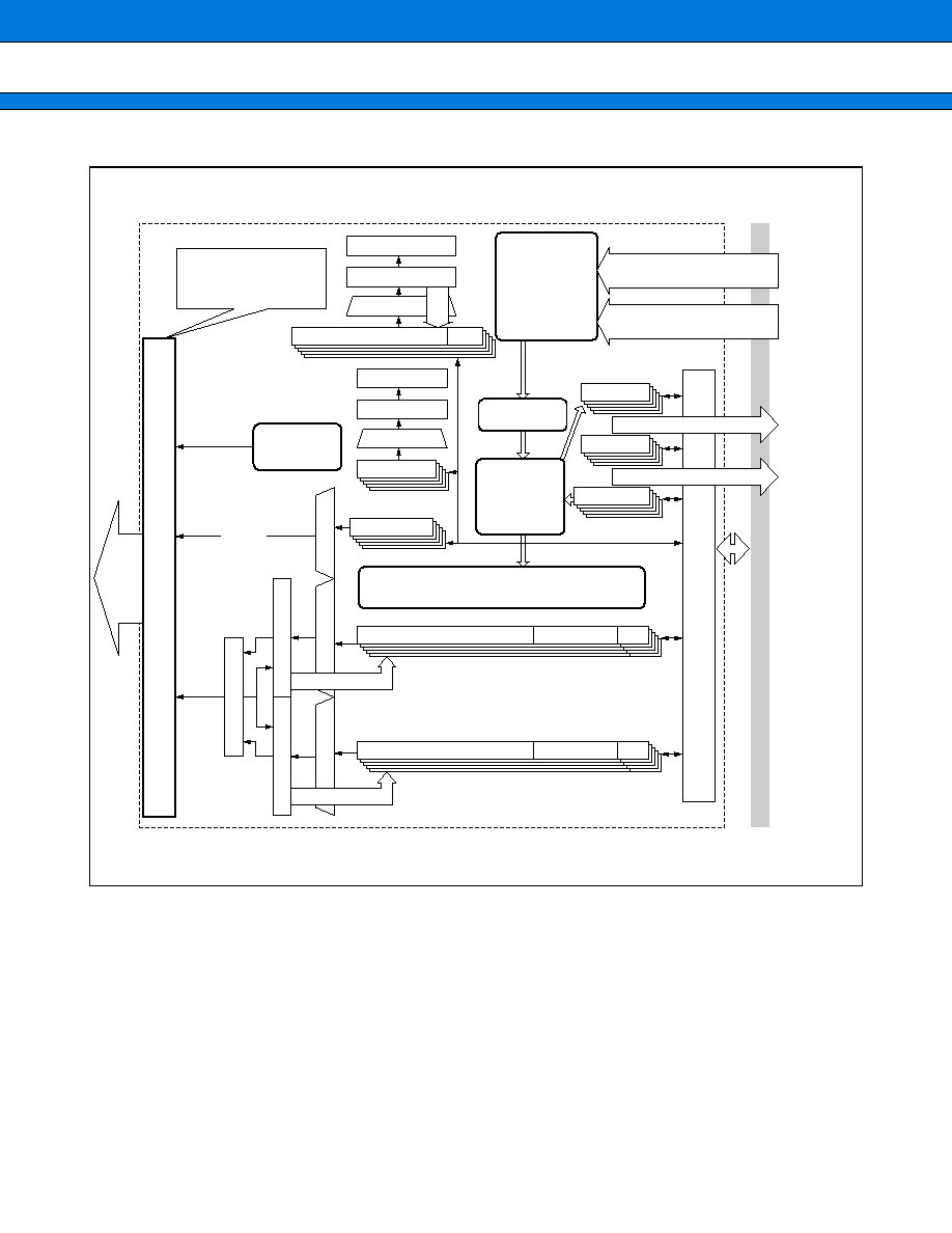
MB91301/MB91V301
78
∑
Block Diagram
Read
Write
DDNO
BLK register
DDNO register
DTCR
DSS [3:0]
ERIR, EDIR
TYPE, MOD, WS
IRQ
[4:0]
MCLREQ
X-bus
DADM, DASZ [7:0] DADR
SDAM, SASZ [7:0] SADR
DMA transfer
request to bus
controller
Read/write
control
To bus
controller
Bus control block
Access
ad-
dress
Addr
ess counter
Counter buffer
Counter buffer
Selector
Selector
Write back
Selector
Buffer
Counter
Selector
Write back
DTC two-stage register
Buffer
Counter
Selector
DMA
start trigger
selection cir-
cuit & request
acknowledge
control
Priority
circuit
Status
transition
circuit
DMA control
DSAD two-stage register
DDAD
two-stage register
Bus control block
Peripheral start request/
Stop input
External pin start
request/Stop input
To interrupt controller
Clear peripheral interrupt
5-channel DMAC block diagram
Write back
MB91301/MB91V301
79
∑
Register List
ch.0 control/status
register A
ch.0 control/status
register B
ch.1 control/status
register A
ch.1 control/status
register B
ch.2 control/status
register A
ch.2 control/status
register B
ch.3 control/status
register A
ch.3 control/status
register B
ch.4 control/status
register A
ch.4 control/status
register B
Overall control register
ch.0 transfer source address register
ch.0 transfer destination address register
ch.1 transfer source address register
ch.1 transfer destination address register
ch.2 transfer source address register
ch.2 transfer destination address register
ch.3 transfer source address register
ch.3 transfer destination address register
ch.4 transfer source address register
ch.4 transfer destination address register
(bit) 31
24 23
16 15
08 07
00
(bit) 31
24 23
16 15
08 07
00
0000200
H
0000204
H
0000208
H
000020C
H
0000210
H
0000214
H
0000218
H
000021C
H
0000220
H
0000224
H
0000240
H
0001000
H
0001004
H
0001008
H
000100C
H
0001010
H
0001014
H
0001018
H
000101C
H
0001020
H
0001024
H
DMACA0
DMACB0
DMACA1
DMACB1
DMACA2
DMACB2
DMACA3
DMACB3
DMACA4
DMACB4
D M A C R
DMASA0
DMADA0
DMASA1
DMADA1
DMASA2
DMADA2
DMASA3
DMADA3
DMASA4
DMADA4
MB91301/MB91V301
80
12. Clock Generation Control
The internal operating clock is generated as follows in MB91301/MB91V301.
∑
Source clock selection : Selects the clock source.
∑
Base clock generation : The base clock is generated by dividing the source clock by 2 or using a PLL.
∑
Generation in each internal block : The base clock is divided to generate the operating clock for each block.
∑
Register List
(Continued)
∑
RSRR : Reset initiation register/Watchdog timer control register
* : Changes depending on what triggered the reset.
◊
: Not initialized
∑
STCR : Standby control register
* : Only when asserted during a reset initiated by the INIT pin. Otherwise, same as INIT.
bit
address : 00000480
H
Initial value (INIT pin)
Initial value (INIT)
Initial value (RST)
bit
address : 00000481
H
Initial value (INIT pin)
Initial value (HST) *
Initial value (INIT)
Initial value (RST)
R
0
X
R
0
X
R
0
X
R/W
0
0
0
R/W
0
0
0
15
14
13
12
11
10
9
8
HSTB
R
1
X
INIT
WDOG
SRST
WT1
WT0
R/W
0
0
0
0
R/W
1
1
1
X
R/W
1
1
1
1
R/W
0
1
X
X
R/W
0
1
X
X
R/W
1
1
1
X
7
6
5
4
3
2
1
0
SLEEP
R/W
0
0
0
0
STOP
HIZ
SRST
OS1
OS0
OSCD1
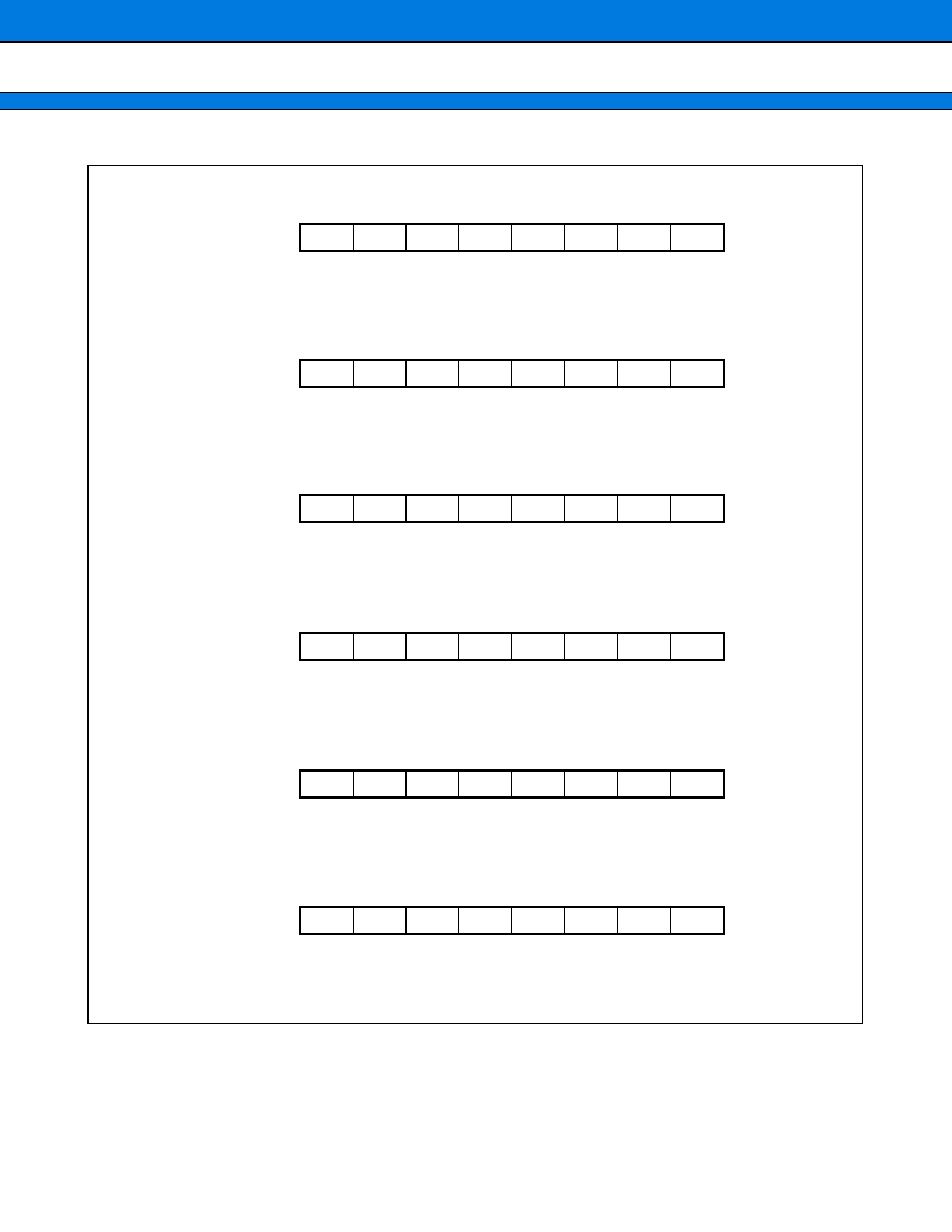
MB91301/MB91V301
81
(Continued)
∑
TBCR : Timebase counter control register
∑
CTBR : Timebase counter clear register
∑
CLKR : Clock source control register
∑
WPR : Watchdog reset generation delay register
∑
DIVR0 : Base clock division setting register 0
∑
DIVR1 : Base clock division setting register 1
bit
address : 00000482
H
Initial value (INIT)
Initial value (RST)
bit
address : 00000483
H
Initial value (INIT)
Initial value (RST)
bit
address : 00000484
H
Initial value (INIT)
Initial value (RST)
bit
address : 00000485
H
Initial value (INIT)
Initial value (RST)
bit
address : 00000486
H
Initial value (INIT)
Initial value (RST)
bit
address : 00000487
H
Initial value (INIT)
Initial value (RST)
R/W
0
0
R/W
X
X
R/W
X
X
R/W
X
X
R/W
0
X
R/W
0
X
15
14
13
12
11
10
9
8
TBIE
R/W
0
0
TBIF
TBC2
TBC1
TBC0
SYNCR SYNCS
W
X
X
W
X
X
W
X
X
W
X
X
W
X
X
W
X
X
W
X
X
7
6
5
4
3
2
1
0
D6
W
X
X
D7
D5
D4
D3
D2
D1
D0
R/W
0
X
R/W
0
X
R/W
0
X
R/W
0
X
R/W
0
X
R/W
0
X
15
14
13
12
11
10
9
8
PLL1S2
PLL1S1 PLL1S0
PLL1EN CLKS1
CLKS0
W
X
X
W
X
X
W
X
X
W
X
X
W
X
X
W
X
X
W
X
X
7
6
5
4
3
2
1
0
D6
W
X
X
D7
D5
D4
D3
D2
D1
D0
R/W
0
X
R/W
0
X
R/W
0
X
R/W
0
X
R/W
0
X
R/W
1
X
R/W
1
X
15
14
13
12
11
10
9
8
B2
R/W
0
X
B3
B1
B0
P3
P2
P1
P0
R/W
0
X
R/W
0
X
R/W
0
X
7
6
5
4
3
2
1
0
T2
R/W
0
X
T3
T1
T0
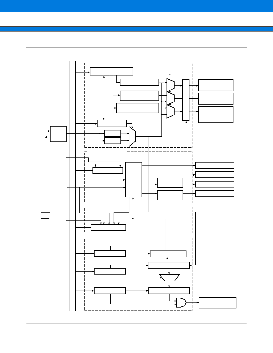
MB91301/MB91V301
82
∑
Block Diagram
X0
X1
PLL
1/2
R
|
B
U
S
DIVR0, 1 register
[Clock generator]
CPU clock division
Stop control
CPU clock
(CLKB)
Peripheral clock
(CLKP)
External bus
clock (CLKT)
Peripheral clock
division
External bus clock
division
CLKR register
Osc
illa-
tion
circu
it
[Stop/sleep
controller]
STCR register
Stop state
Internal interrupt
Internal reset
State
transi-
tion
con-
trol cir-
cuit
SLEEP state
Reset F/F
Reset F/F
Internal reset (RST)
Internal reset (INIT)
[Reset circuit]
RSRR register
WPR register
CTBR register
Watchdog F/F
TBCR register
Timebase counter
Overflow detection F/F
Interrupt enable
[Watchdog controller]
Timebase timer
interrupt request
Selec-
to
r
Selector
HST pin
RST pin
INIT pin
Selector
Count clock
Selec-
tor
Selec-
tor
MB91301/MB91V301
83
s
ELECTRICAL CHARACTERISTICS
1.
Absolute Maximum Ratings
(V
SS
=
AV
SS
=
0 V)
*1 : V
CC
must not be lower than V
SS
-
0.3 V.
*2 : AV
CC
, AVRH and AVRL should not exceed V
CC
+
0.3 V, including at power-on. AVRH and AVRL should not exceed
AV
CC
. Also AVRL should not exceed AVRH.
*3 : The maximum output current is the peak value for a single pin.
*4 : The average output current is the average current for a single pin over a period of 100ms.
*5 : The total average output current is the average current for all pins over a period of 100ms.
WARNING: Semiconductor devices can be permanently damaged by application of stress (voltage, current,
temperature, etc.) in excess of absolute maximum ratings. Do not exceed these ratings.
Parameter
Symbol
Rating
Unit
Remaeks
Min
Max
Supply voltage
V
CC
V
SS
-
0.5
V
SS
+
4.0
V
*1
Analog supply voltage
AV
CC
V
SS
-
0.5
V
SS
+
4.0
V
*2
Analog reference voltage
AVRH,
AVRL
V
SS
-
0.5
AV
CC
V
*2
Input voltage
V
I
V
SS
-
0.3
V
CC
+
0.3
V
Analog pin input voltage
V
IA
V
SS
-
0.3
AV
CC
+
0.3
V
Output voltage
V
OH
V
SS
-
0.3
V
CC
+
0.3
V
"L" level maximum output
current
I
OL
10
mA
*3
"L" level average output current
I
OLAV
8
mA
*4
"L" level total maximum output
current
I
OL
100
mA
"L" level total average output
current
I
OLAV
50
mA
*5
"H" level maximum output
current
I
OH
-
10
mA
*3
"H" level average output current
I
OHAV
-
4
mA
*4
"H" level total maximum output
current
I
OH
-
50
mA
"H" level total average output
current
I
OHAV
-
20
mA
*5
Power consumption
P
D
1000
mW
Operating temperature
Ta
0
+
70
∞
C
Storage temperature
T
STG
-
50
+
150
∞
C
MB91301/MB91V301
84
2.
Recommended Operating Conditions
(V
SS
=
AV
SS
=
0 V)
<Notes on turning the power on>
The maximum power rising slope (
V/
t) must be 0.05 V/
µ
s when the 3 V power supply is turned on.
It takes about 100
µ
s until the 2.5 V power supply becomes stable after the 3 V power supply becomes stable.
Keep INIT input during that interval.
WARNING: The recommended operating conditions are required in order to ensure the normal operation of the
semiconductor device. All of the device's electrical characteristics are warranted when the device is
operated within these ranges.
Always use semiconductor devices within their recommended operating condition ranges. Operation
outside these ranges may adversely affect reliability and could result in device failure.
No warranty is made with respect to uses, operating conditions, or combinations not represented on
the data sheet. Users considering application outside the listed conditions are advised to contact their
FUJITSU representatives beforehand.
Parameter
Symbol
Value
Unit
Remarks
Min
Max
Supply voltage
V
CC
3.0
3.6
V
Normal operation
Analog supply voltage
AV
CC
V
SS
+
3
3.6
V
Analog reference voltage
AVRH
AV
SS
AV
CC
V
AVRL
AV
SS
AVRH
V
Operating temperature
Ta
0
+
70
∞
C
MB91301/MB91V301
85
3.
DC Characteristics
(V
CC
=
3.0 V to 3.6 V , V
SS
=
AV
SS
=
0 V, Ta
=
0
∞
C to
+
70
∞
C)
*1 : Excludes X0, X1, pins with internal pull-up resistor (INIT, TRST), and pins with a pull-up resistor set by PCR.
*2 : Values enclosed in brackets ( ) are for the MB91V301.
Parameter
Sym-
bol
Pin name
Condition
Value
Unit
Remarks
Min
Typ
Max
"H" level input
voltage
V
IH
Non-hystere-
sis input pin
2.0
V
CC
+
0.3
V
V
IHS
Hysteresis
input pin
0.8
◊
V
CC
V
CC
+
0.3
V
Hysteresis input
"L" level input
voltage
V
IL
Non-hystere-
sis input pin
V
SS
0.8
V
V
ILS
Hysteresis
input pin
V
SS
0.2
◊
V
CC
V
Hysteresis input
"H" level output
voltage
V
OH
All output pins
V
CC
=
3.0 V
I
OH
=
-
4.0 mA
V
CC
-
0.4
V
CC
V
"L" level output
voltage
V
OL
All output pins
V
CC
=
3.0 V
I
OL
=
4.0 mA
V
SS
0.4
V
Input leak
current
(Hi-Z output
leak current)
I
LI
All input pins*
1
V
CC
=
3.6 V
0.45 V
<
V
I
<
V
CC
-
5
+
5
µ
A
Pull-up
resistance
R
UP
With pins Pull-
up settings
V
CC
=
3.6 V
V
I
=
0.45 V
10
25
120
k
Power supply
current*
2
I
CC
V
CC
f
C
=
17 MHz
V
CC
=
3.6 V
110
(160)
150
(220)
mA
When operating at :
CLKB : 68 MHz
CLKT : 68 MHz
CLKP : 34 MHz
(
◊
4 multiplier)
I
CCS
f
C
=
17 MHz
V
CC
=
3.6 V
50
(75)
90
(130)
mA
When sleeping at :
CLKP : 34 MHz
in sleep mode
I
CCH
Ta
=
+
25
∞
C
V
CC
=
3.6 V
200
(300)
700
(
)
µ
A
In stop mode
Input
capacitance
C
IN
Except for
V
CC
V
SS
AV
CC
AV
SS
AVRH
AVR
10
pF
MB91301/MB91V301
86
4.
AC Characteristics
(1) Clock Timing Ratings
(V
CC
=
3.0 V to 3.6 V , V
SS
=
AV
SS
=
0 V, Ta
=
0
∞
C to
+
70
∞
C)
* : Values are for minimum clock frequency (12.5 MHz) input to X0, oscillation circuit uses PLL, and gear ratio
=
1/16.
∑
Conditions for measuring the clock timing ratings
∑
Warranted operation range
Parameter
Sym-
bol
Pin
name
Condi-
tion
Value
Unit
Remarks
Min
Max
Clock frequency (1)
f
C
X0,
X1
12.5
17
MHz
Using PLL
(When operating at max in-
ternal frequency (68 MHz)
=
17 MHz self-oscillation with
◊
4 PLL)
Clock cycle time
t
C
X0,
X1
58.8
ns
Clock frequency (2)
f
C
X0,
X1
10
34
MHz
Self-oscillation (1/2 division
input)
Internal operation clock
frequency
f
CP
0.78*
68
MHz
CPU
f
CPP
0.78*
34
MHz
Peripherals
f
CPT
0.78*
68
MHz
External bus
Internal operation clock
cycle time
t
CP
14.7
1280*
ns
CPU
t
CPP
29.4
1280*
ns
Peripherals
t
CPT
14.7
1280*
ns
External bus
0.8 V
CC
t
C
C
=
50 pF
Output pin
0
(MHz)
3.6
3.0
f
CP
/ f
CPP
68
34
0.78
V
CC
(V)
Internal clock
Power supply
Warranted operation range (Ta
=
0
∞
C to
+
70
∞
C)
f
CPP
is represented by the shaded area.
MB91301/MB91V301
87
∑
External/internal clock setting range
70
60
50
40
30
20
10
0
68
48
34
fcpp
fcp, fcpt
MHz
24
22.7
17
5
0
20
30
fc
MHz
10
12.5
17
34
5 multiplier (CPU)
Notes :
∑
If using the PLL, input an external clock in the range 12.5 MHz to 17 MHz.
∑
Allow a PLL oscillation stabilization time
>
300
µ
s.
∑
Set the gear ratio for the internal clock to be within the values shown in the "(1) Clock Timing Ratings"
table.
4 multiplier (CPU)
3 multiplier (CPU)
5 multiplier, 2 divide
(CPU, peripheral)
4 multiplier, 2 divide
(CPU, peripheral)
3 multiplier, 2 divide
(CPU, peripheral)
4 multiplier, 3 divide
(CPU, peripheral)
4 multiplier, 4 divide
(CPU, peripheral)
5 multiplier, 3 divide
(CPU, peripheral)
1/2 divide
PLL
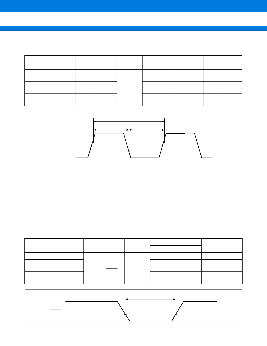
MB91301/MB91V301
88
(2) Clock Output Timing
(V
CC
=
3.0 V to 3.6 V, V
SS
=
AV
SS
=
0 V, Ta
=
0
∞
C to
+
70
∞
C)
*1 : t
CYC
is the frequency of one clock cycle after gearing.
*2 : The following ratings are for the gear ratio set to
◊
1.
For the ratings when the gear ratio is set to between 1/2, 1/4 and 1/8, substitute 1/2, 1/4 or 1/8 for n in the
following equation.
Min : (1
/
2
◊
1
/
n)
◊
t
CYC
-
2.35
Max : (1
/
2
◊
1
/
n)
◊
t
CYC
+
2.65
*3 : The following rating are for the gear ratio set to
◊
1.
Min : (1
/
2
◊
1
/
n)
◊
t
CYC
-
2.35
Max : (1
/
2
◊
1
/
n)
◊
t
CYC
+
2.65
(3) Reset and Tool Reset Input Ratings
(V
CC
=
3.0 V to 3.6 V , V
SS
=
AV
SS
=
0 V, Ta
=
0
∞
C to
+
70
∞
C)
Parameter
Sym-
bol
Pin name
Condition
Value
Unit
Remarks
Min
Max
Cycle time
t
CYC
SYSCLK,
MCLK
t
CPT
ns
*1
SYSCLK
SYSCLK
t
CHCL
SYSCLK,
MCLK
t
CYC
-
2.35
t
CYC
+
2.65
ns
*2
SYSCLK
SYSCLK
t
CLCH
SYSCLK,
MCLK
t
CYC
-
2.35
t
CYC
+
2.65
ns
*3
Parameter
Sym-
bol
Pin name
Condition
Value
Unit
Remarks
Min
Max
Init input time (at power-on)
t
INTL
INIT,
TRST
20
+
µ
s
Init input time
( other than at power-on)
t
CP
◊
5
ns
Init input time
(recovery from stop)
20
+
µ
s
1
2
1
2
1
2
1
2
SYSCLK
MCLK
VOH
VOL
VOH
t
CYC
t
CLCH
t
CHCL
TRST
0.2 V
CC
t
INTL
INIT
MB91301/MB91V301
89
(4) Normal Bus Access Read/Write Operation
(V
CC
=
3.0 V to 3.6 V , V
SS
=
AV
SS
=
0 V, Ta
=
0
∞
C to
+
70
∞
C)
* : When the bus is delayed by automatic wait insertion or RDY input, add (t
CYC
◊
number of wait cycles) to the rated
values.
Parameter
Sym-
bol
Pin name
Condition
Value
Unit Remarks
Min
Max
CS0 to CS7 setup
t
CSLCH
SYSCLK,
CS0 to CS7
3
ns
CS0 to CS7 hold
t
CHCSH
3
t
CYC
/
2
+
4
ns
Address setup
t
ASCH
SYSCLK,
A23 to A00
3
ns
t
ASWL
WR0 to WR3,
A23 to A00
4
ns
t
ASRL
RD, A23 to A00
5
ns
Address hold
t
CHAX
SYSCLK,
A23 to A00
3
t
CYC
/
2
+
4
ns
t
WHAX
WR0 to WR3,
A23 to A00
t
CYC
/
2
-
5
ns
t
RHAX
RD, A23 to A00
t
CYC
/
2
-
7
ns
Valid address
Valid data input time
t
AVDV
A23 to A00,
D31 to D00
3
/
2
◊
t
CYC
-
11
ns
*
WR0 to WR3 delay time
t
CHWL
SYSCLK, WR,
WR0 to WR3
6
ns
WR0 to WR3 delay time
t
CHWH
6
ns
WR0 to WR3 minimum pulse
width
t
WLWH
WR,
WR0 to WR3
t
CYC
-
5
ns
Data setup
WRx
t
DSWH
WR,
WR0 to WR3,
D31 to D00
t
CYC
ns
WRx
Data hold time
t
WHDX
5
ns
RD delay time
t
CHRL
SYSCLK,
RD
6
ns
RD delay time
t
CHRH
10
ns
RD
Valid data input time
t
RLDV
RD,
D31 to D00
t
CYC
-
10
ns
*
Data setup
RD
time
t
DSRH
10
ns
RD
Data hold time
t
RHDX
0
ns
RD minimum pulse width
t
RLRH
RD
t
CYC
-
5
ns
AS setup
t
ASLCH
SYSCLK,
AS
t
CYC
/
2
-
6
ns
AS hold
t
CHASH
3
ns
UUB/ULB/LUB/LLB set up
t
BLCH
SYSCLK
,
UUB
/
ULB
/
LUB
/
LLB
t
CYC
/
2
-
6
ns
UUB/ULB/LUB/LLB hold
t
CHBH
3
ns
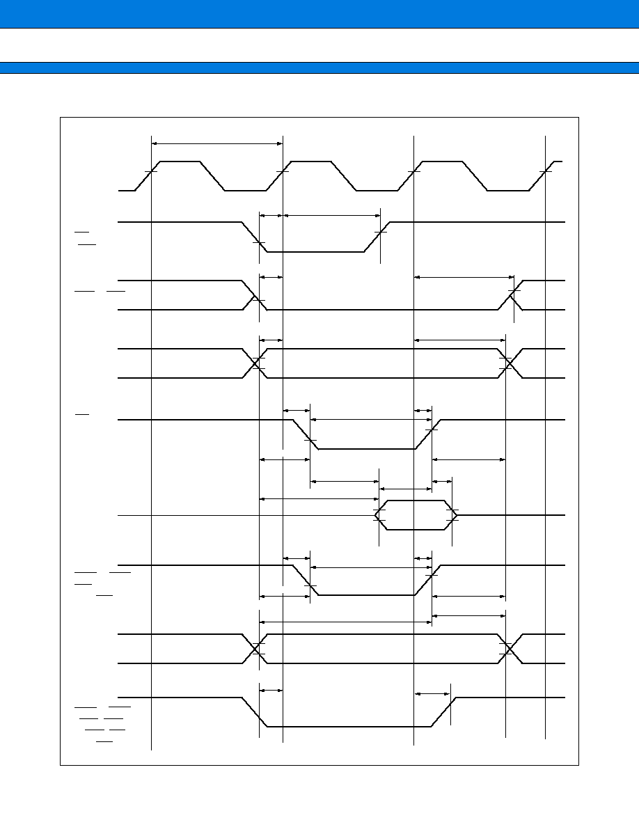
MB91301/MB91V301
90
MCLK
SYSCLK
CS0 to CS7
V
OH
V
OH
V
OH
V
OL
V
OL
V
OH
V
OH
V
OL
V
OH
V
OL
V
OL
V
OL
A23 to A00
RD
D31 to D00
WR0 to WR3
WR
(use WR strobe)
D31 to D00
V
OH
V
OH
V
OH
V
OH
V
OL
V
OH
V
OL
V
OH
V
OL
V
OH
t
ASCH
t
AVDV
t
RLDV
t
DSRH
t
RHDX
t
WLWH
t
CHWL
t
CHWH
t
CHAX
t
CHRH
t
DSWH
t
WHDX
t
CYC
t
BLCH
t
CHCSH
t
CSLCH
t
CHRL
t
RLRH
AS
(LBA)
V
OL
V
OH
t
CHASH
t
ASLCH
BA1
t
ASRL
t
RHAX
t
ASWL
t
WHAX
WR0 to WR3
(UUB, ULB,
LUB, LLB)
(use WR strobe)
t
CHBH
Write
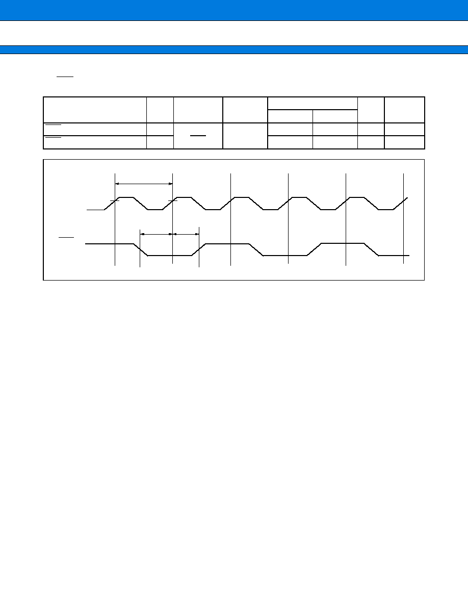
MB91301/MB91V301
91
(5) BAA Timing
(V
CC
=
3.0 V to 3.6 V, V
SS
=
AV
SS
=
0 V, Ta
=
0
∞
C to
+
70
∞
C)
Parameter
Sym-
bol
Pin name
Condition
Value
Unit
Remarks
Min
Max
BAA setup
t
CHBAH
SYSCLK,
BAA
t
CYC
/
2
-
6
ns
BAA hold
t
CHBAL
3
ns
MCLK
SYSCLK
BAA
V
OH
V
OH
t
CYC
t
CHBAH
t
CHBAL
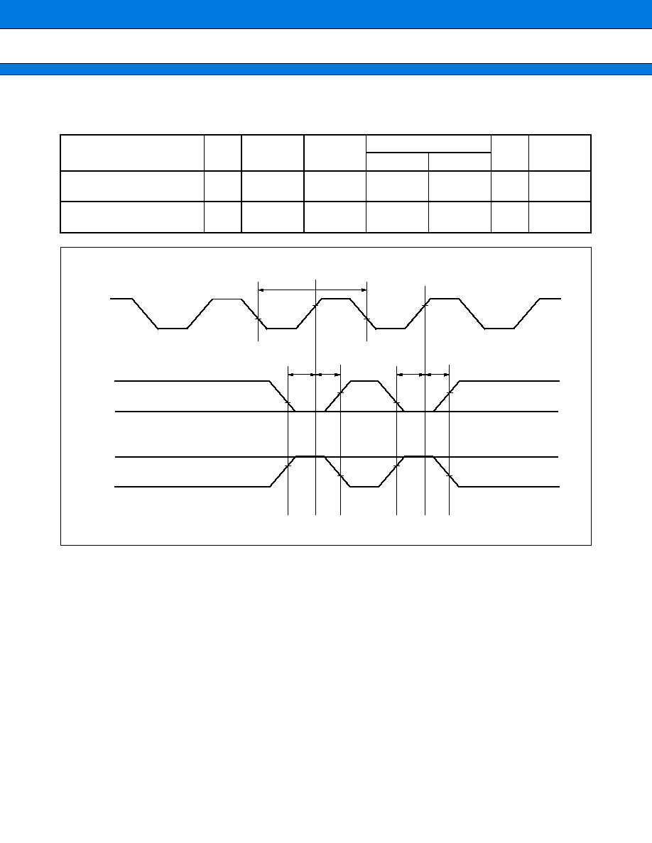
MB91301/MB91V301
92
(6) Ready Input Timings
(V
CC
=
3.0 V to 3.6 V, V
SS
=
AV
SS
=
0 V, Ta
=
0
∞
C to
+
70
∞
C)
Parameter
Sym-
bol
Pin name
Condition
Value
Unit
Remarks
Min
Max
RDY setup time
SYSCLK
t
RDYS
SYSCLK
RDY
10
ns
SYSCLK
RDY hold time
t
RDYH
SYSCLK
RDY
0
ns
SYSCLK
MCLK
V
OH
V
OH
V
OL
V
OL
V
OL
V
OH
V
OL
V
OH
V
OH
V
OL
V
OH
V
OL
t
RDYH
t
RDYH
RDY
RDY
t
CYC
t
RDYS
t
RDYS
(Wait specified
by RDY)
(No wait specified
by RDY)
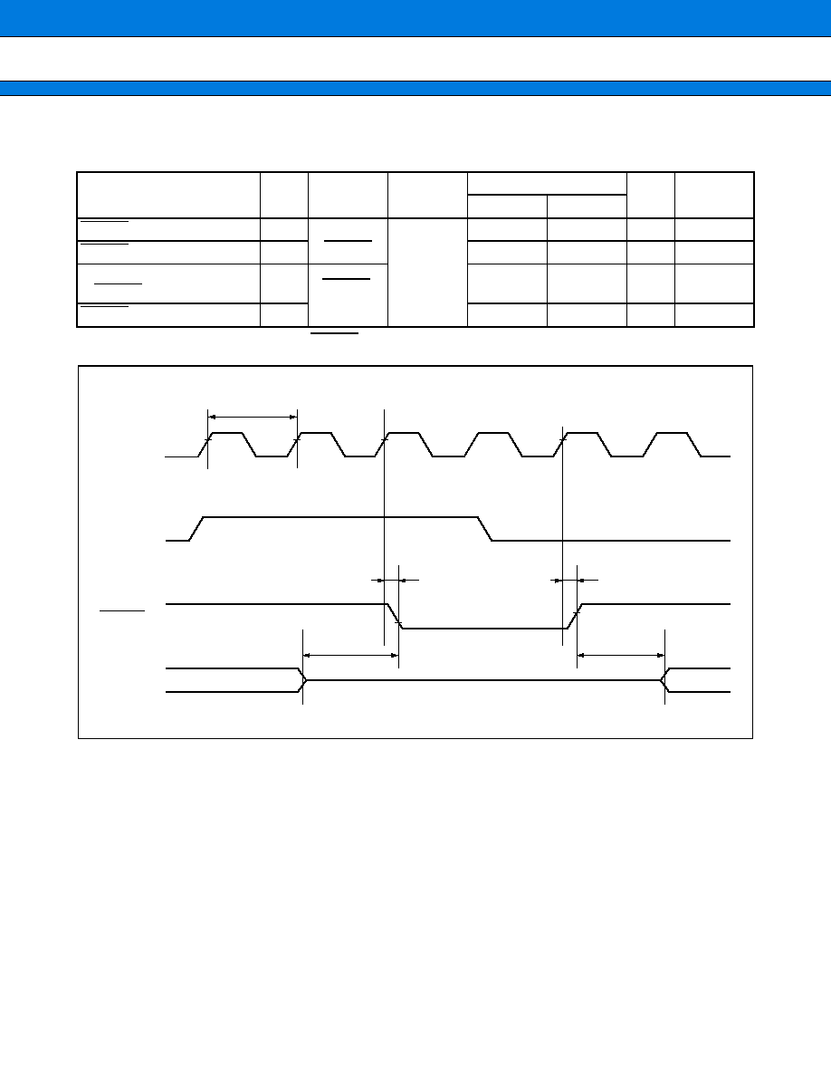
MB91301/MB91V301
93
(7) Hold Timing
(V
CC
=
3.0 V to 3.6 V, V
SS
=
AV
SS
=
0 V, Ta
=
0
∞
C to
+
70
∞
C)
Note : The time from receiving BRQ to BGRNT changing is one cycle or more.
Parameter
Sym-
bol
Pin name
Condition
Value
Unit
Remarks
Min
Max
BGRNT delay time
t
CHBGL
SYSCLK,
BGRNT
6
ns
BGRNT delay time
t
CHBGH
6
ns
Pin floating
BGRNT
time
t
XHAL
BGRNT,
each pins
t
CYC
-
10
t
CYC
+
10
ns
BGRNT
pin valid time
t
HAHV
t
CYC
-
10
t
CYC
+
10
ns
SYSCLK
MCLK
V
OH
t
CHBGL
V
OL
V
OH
V
OH
V
OH
V
OH
t
CHBGH
BRQ
BGRNT
t
CYC
t
HAHV
t
HXAL
Other pins
High-Z
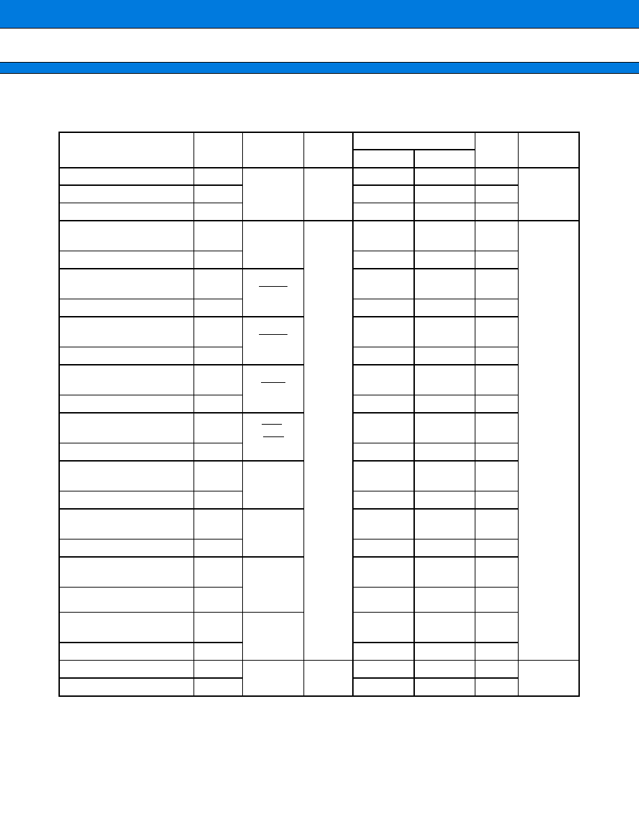
MB91301/MB91V301
94
(8) SDRAM Timing
(V
CC
=
3.0 V to 3.6 V , V
SS
=
AV
SS
=
0 V, Ta
=
0
∞
C to
+
70
∞
C)
Parameter
Symbol
Pin name
Condi-
tion
Value
Unit
Remarks
Min
Max
Output clock cycle time
t
CYCSD
MCLK
68
MHz
"H" level clock pulse width
t
CHSD
5
ns
"L" level clock pulse width
t
CLSD
5
ns
MCLKO
output delay
time
t
ODSDCKE
MCLKE
11
ns
Output hold time
t
OHSDCKE
2
ns
MCLKO
output delay
time
t
ODSDRAS
SRAS
11
ns
Output hold time
t
OHSDRAS
2
ns
MCLKO
output delay
time
t
ODSDCAS
SCAS
11
ns
Output hold time
t
OHSDCAS
2
ns
MCLKO
output delay
time
t
ODSDWE
SWE
11
ns
Output hold time
t
OHSDWE
2
ns
MCLKO
output delay
time
t
ODSDCS
CS6,
CS7
11
ns
Output hold time
t
OHSDCS
2
ns
MCLKO
output delay
time
t
ODSDA
A0 to A13
11
ns
Output hold time
t
OHSDA
2
ns
MCLKO
output delay
time
t
ODSDBA
A14,
A15
11
ns
Output hold time
t
OHSDBA
2
ns
MCLKO
output delay
time
t
ODSDDQM
DQMUU,
DQMUL,
DQMLU,
DQMLL
11
ns
Output hold time
t
OHSDDQM
2
ns
MCLKO
output delay
time
t
ODSDD
D00 to D31
11
ns
Output hold time
t
OHSDD
2
ns
Data input setup time
t
ISSDD
D00 to D31
4
ns
Data input hold time
t
IHSDD
2
ns
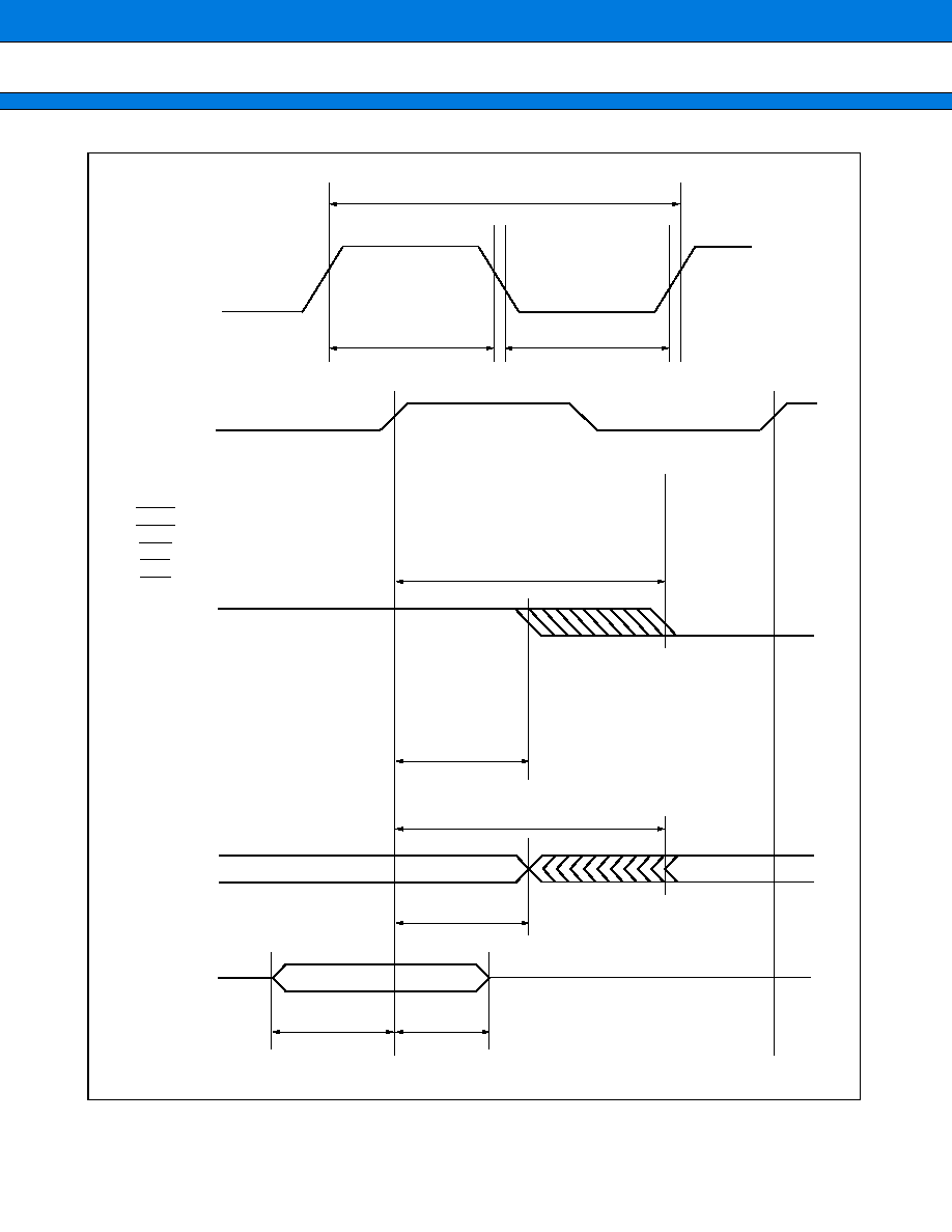
MB91301/MB91V301
95
MCLKO
MCLKO
MCLKE
SRAS
SCAS
SWE
CS6
CS7
A00 to A15
DQMUU
DQMUL
DQMLU
DQMLL
t
CYCSD
t
ODSDCKE
t
ODSDRAS
t
ODSDCAS
t
ODSDWE
t
ODSDCS
t
ODSDA
t
ODSDDQM
t
OHSDCKE
t
OHSDRAS
t
OHSDCAS
t
OHSDWE
t
OHSDCS
t
OHSDA
t
OHSDDQM
t
ODSDD
t
OHSDD
t
ISSDD
t
IHSDD
t
CHSD
t
CLSD
D00 to D31
output
D00 to D31
input
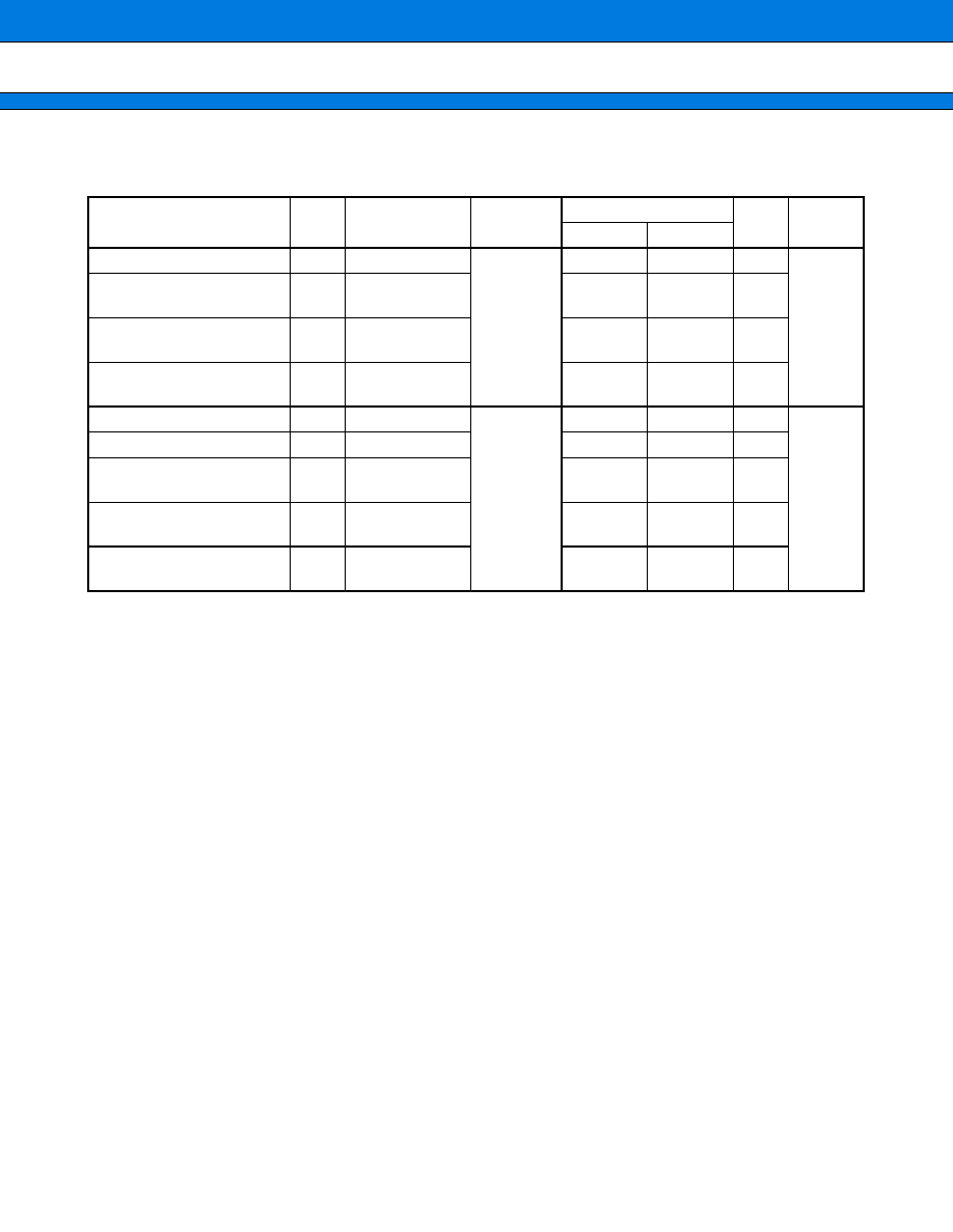
MB91301/MB91V301
96
(9) UART Timing
(V
CC
=
3.0 V to 3.6 V, V
SS
=
AV
SS
=
0 V, Ta
=
0
∞
C to
+
70
∞
C)
Notes :
∑
These are the AC ratings for CLK synchronous mode.
∑
t
CYCP
is the peripheral clock cycle time.
Parameter
Sym-
bol
Pin name
Condition
Value
Unit
Remarks
Min
Max
Serial clock cycle time
t
SCYC
SCK0 to SCK2
Internal
shift clock
mode
8 t
CYCP
ns
SCK
SO delay time
t
SLOV
SCK0 to SCK2,
SOT0 to SOT2
-
80
+
80
ns
Valid SI
SCK
t
IVSH
SCK0 to SCK2,
SIN0 to SIN2
100
ns
SCK
valid SIN hold time
t
SHIX
SCK0 to SCK2,
SIN0 to SIN2
60
ns
Serial clock "H" pulse width
t
SHSL
SCK0 to SCK2
External
shift clock
mode
4 t
CYCP
ns
Serial clock "L" pulse width
t
SLSH
SCK0 to SCK2
4 t
CYCP
ns
SCK
SOT delay time
t
SLOV
SCK0 to SCK2,
SOT0 to SOT2
150
ns
Valid SIN
SCK
t
IVSH
SCK0 to SCK2,
SIN0 to SIN2
60
ns
SCK
valid SIN hold time
t
SHIX
SCK0 to SCK2,
SIN0 to SIN2
60
ns
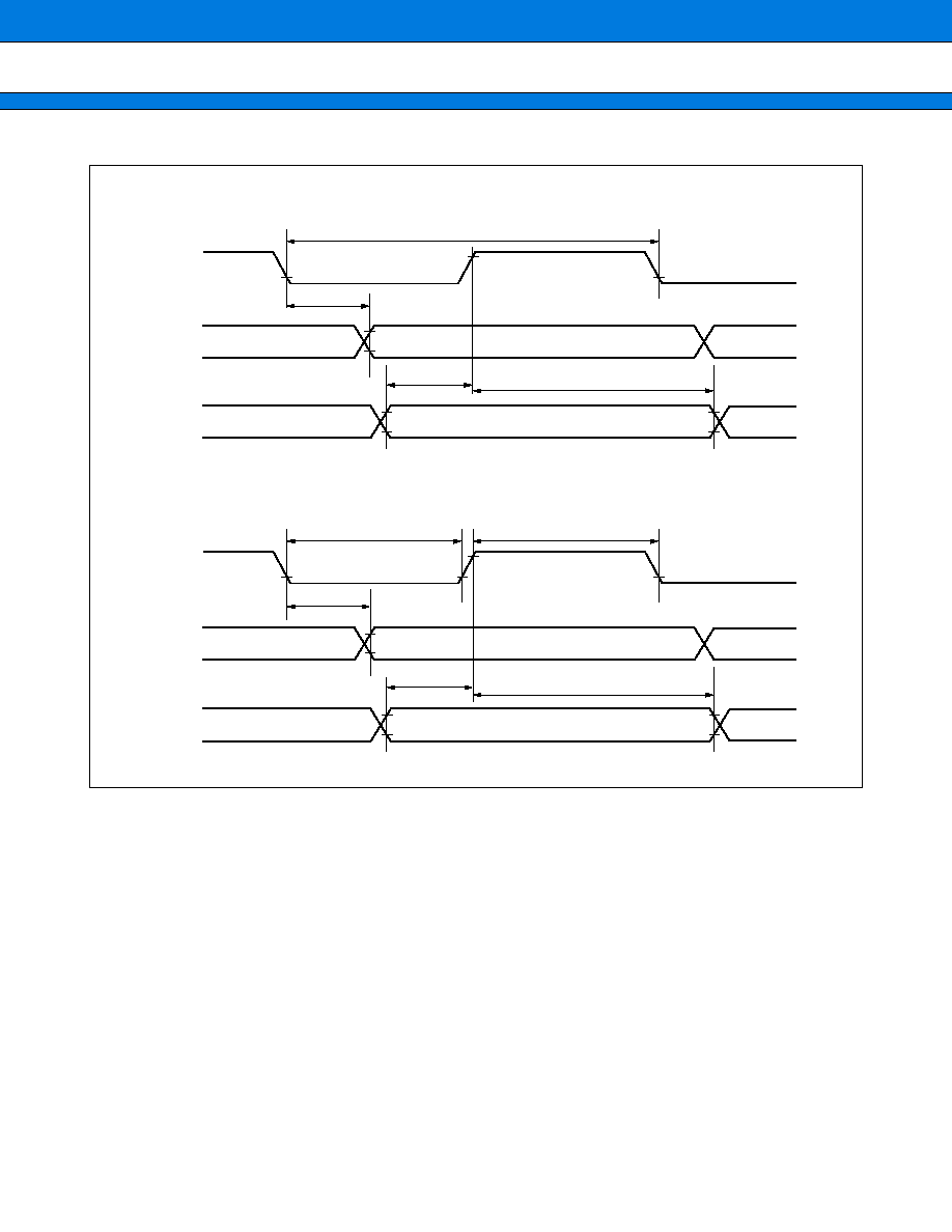
MB91301/MB91V301
97
∑
Internal shift clock mode
∑
External shift clock mode
SCK0, 1, 2
SOT0, 1, 2
SIN0, 1, 2
t
SCYC
t
SLOV
t
IVSH
t
SHIX
V
OL
V
OH
V
OL
V
OH
V
OL
V
OH
V
OL
V
OH
V
OL
SCK0, 1, 2
SOT0, 1, 2
SIN0, 1, 2
t
SLOV
t
SLSH
t
SHSL
t
IVSH
t
SHIX
V
OH
V
OL
V
OH
V
OL
V
OL
V
OL
V
OH
V
OL
V
OH
V
OL
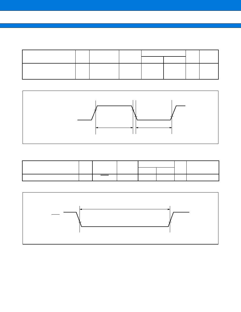
MB91301/MB91V301
98
(10) Reload Timer Clock and PPG Timer Input Timings
(V
CC
=
3.0 V to 3.6 V, V
SS
=
AV
SS
=
0 V, Ta
=
0
∞
C to
+
70
∞
C)
Note : t
CYCP
is the peripheral clock cycle time.
(11) Trigger Input Timing
(V
CC
=
3.0 V to 3.6 V, V
SS
=
AV
SS
=
0 V, Ta
=
0
∞
C to
+
70
∞
C)
Note : t
CYCP
is the peripheral clock cycle time.
Parameter
Sym-
bol
Pin name
Condition
Value
Unit
Remarks
Min
Max
Input pulse width
t
TIWH
t
TIWL
TIN0 to TIN2,
PPG0 to PPG3,
TRG0 to TRG3
2 t
CYCP
ns
Parameter
Sym-
bol
Pin name
Condition
Value
Unit
Remarks
Min
Max
A/D activation trigger input time
t
ATGL
ATG
5 t
CYCP
ns
t
TIWH
V
IH
V
IH
V
IL
V
IL
t
TIWL
TIN0 to TIN2
PPG0 to PPG3
TRG0 to TRG3
ATG
t
ATGL
V
IL
V
IL
MB91301/MB91V301
99
(12) DMA Controller Timing
(V
CC
=
3.0 V to 3.6 V, V
SS
=
AV
SS
=
0 V, Ta
=
0
∞
C to
+
70
∞
C)
[ For edge detection ] (Block/step transfer mode, burst transfer mode)
Note : When f
CPT
>
f
CP
, t
CYC
becomes same as t
CP
.
[ For level detection ] (Demand transfer mode)
[ For all operation modes ]
Parameter
Sym-
bol
Pin name
Condition
Value
Unit
Remarks
Min
Max
DREQ input pulse width
t
DRWL
DREQ 0, DREQ1
2 t
CYC
ns
Parameter
Sym-
bol
Pin name
Condition
Value
Unit
Remarks
Min
Max
DSTP setup time
t
DREQS
SYSCLK,
DREQ 0, DREQ1
10
ns
DSTP hold time
t
DREQH
SYSCLK,
DREQ 0, DREQ1
0.0
ns
Parameter
Sym-
bol
Pin name
Condition
Value
Unit
Remarks
Min
Max
DACK delay time
t
CLDL
SYSCLK, DACK 0,
DACK1
10
ns
t
CLDH
10
DEOP delay time
t
CLEL
SYSCLK, DEOP 0,
DEOP1
10
ns
t
CLEH
10
IORD delay time
t
CLIRL
SYSCLK,
IORD
10
ns
t
CLIRH
10
IOWR delay time
t
CLIWL
SYSCLK,
IOWR
10
ns
t
CLIWH
10
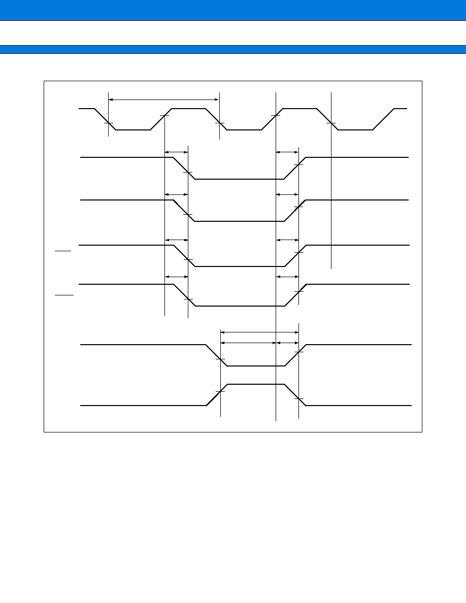
MB91301/MB91V301
100
SYSCLK
MCLK
DACK0, DACK1
DREQ0, DREQ1
DREQ0, DREQ1
IORD
V
OL
V
OH
V
OL
V
OL
V
OH
V
OL
V
OH
V
OL
V
OH
V
OL
V
OH
V
OL
V
OH
V
OL
V
OH
t
CLIRL
t
CLIWL
t
CLDL
t
CYC
t
CLIRH
t
CLIWH
t
DREQS
t
DREQH
t
DRWL
t
CLDH
DEOP0, DEOP1
V
OL
V
OH
t
CLEL
t
CLEH
IOWR
MB91301/MB91V301
101
5.
Electrical Characteristics for the A/D Converter
(V
CC
=
AV
CC
=
3.0 V to 3.6 V, V
SS
=
AV
SS
=
0 V, AVRH
=
3.0 V to 3.6 V , Ta
=
0
∞
C to
+
70
∞
C)
*1 : For V
CC
=
AV
CC
=
3.0 V to 3.6 V , machine clock
=
34 MHz
*2 : Current when A/D converter not operating and CPU in stop mode (V
CC
=
AV
CC
=
AVRH
=
3.6 V)
Notes :
∑
The relative error increases as AVRH becomes smaller.
∑
Ensure that the output impedance of the external circuit connected to the analog input meets the following
condition :
Output impedance of external circuit
<
7 k
If the output impedance of the external circuit is too high, the analog voltage sampling time may be too
short.
Parameter
Symbol
Pin name
Value
Unit
Min
Typ
Max
Resolution
10
BIT
Total error
-
8.5
+
8.5
LSB
Linearity error
-
3.0
+
3.0
LSB
Differential linearity error
-
2.5
+
2.5
LSB
Zero transition error
V
OT
AN0 to AN3
-
8.0
+
0.5
+
8.0
LSB
Full-scale transition error
V
FST
AN0 to AN3
AVRH
-
8.0
AVRH
-
1.5
AVRH
+
8.0
LSB
Conversion time*
1
4.1
µ
s
machine
clock (CLKP)
34 MHz at
operating
µ
s
Analog port input current
I
AIN
AN0 to AN3
0.1
10
µ
A
Analog input voltage
V
AIN
AN0 to AN3
AVss
AVRH
V
Reference voltage
AVRH
AVss
AV
CC
V
Power supply current
I
A
AV
CC
0.6
2
mA
I
AH
*
2
10
µ
A
Reference voltage supply current
I
R
AVRH
0.6
2
mA
I
RH
*
2
10
µ
A
Variation between channels
AN0 to AN3
5
LSB
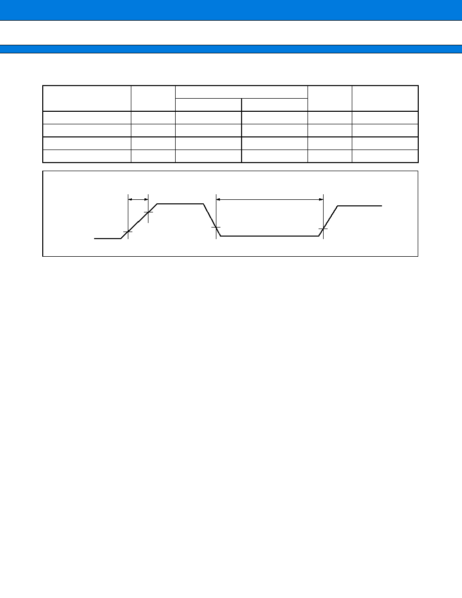
MB91301/MB91V301
102
6.
Power-on ratings
Parameter
Symbol
Value
Unit
Remarks
Min
Max
Power rise time
tr
38
ms
Tilt
=
0.05 V
/
ms
Power start time
Voff
0.1
V
Power end voltage
Von
2.0
V
Power shutdown time
toff
1
ms
V
CC
tr
t
off
V
on
V
off

MB91301/MB91V301
103
s
PIN STATUS IN EACH CPU STATE
∑
Terms used in the pin status list
∑ Input ready
Indicates that the input function can be used.
∑ Input 0 fixed
Indicates that the input level has been internally fixed to be 0 to prevent leakage when the input is released.
∑ Output Hi-Z
Indicates to put the pin in a high impedance state with the pin driving transistor disabled for driving.
∑ Output held
Indicates the output in the output state existing immediately before this mode is established.
If the device enters this mode with an internal output peripheral operating or while serving as an output port,
the output is performed by the internal peripheral or the port output is maintained, respectively.
∑ Previous state held
When the device serves for output or input immediately before entering this mode, the device maintains the
output or is ready for the input, respectively.
MB91301/MB91V301
104
∑
Pin Status List (External bus : 32 bit bus width)
(Continued)
Pin no.
Port
name
Specified
function
name
Function
name
At initialization (INIT)
Sleep
mode
Stop mode
Bus released
(BGRNT)
Function
name
Initial
value
HIZ
=
=
=
=
0
HIZ
=
=
=
=
1
Bus width
32 bit
Bus width
8 bit
CS
shared
CS not
shared
1 to 5
P13 to P17
D11 to D15
D11 to D15
P13 to P17
Output Hi-Z
Input ready
P : Previous
state held
F : Output
held or Hi-Z
P : Previous
state held
F : Output
held or Hi-Z
Output Hi-
Z/input 0
fixed
Output Hi-Z
Output Hi-Z
8 to 15
P20 to P27
D16 to D23
D16 to D23
P20 to P27
18 to 25
P30 to P37
D24 to D31
D24 to D31
P30 to P37
8
P80
RDY
P80
P80
Output Hi-Z
Input ready
P : Previous
state held
F : RDY input
Previous
state held
Output Hi-
Z/input 0
fixed
P : Previous
state held
F : RDY
input
P : Previous
state held
F : RDY
input
29
P81
BGRNT
P81
P81
P : Previous
state held
F : H output
L output
L output
30
P82
BRQ
P82
P82
P : Previous
state held
F : BRQ input
invalid
BRQ input
BRQ input
31
P83
RD
RD
RD
H output
P : Previous
state held
F : H output
Previous
state held
Output Hi-Z
Output Hi-Z
32
P84
DQMUU/WR0
DQMUU/WR0
DQMUU/WR0
33
P85
DQMUL/WR1
DQMUL/WR1
P85
F : H output
34
P86
DQMLU/WR2
DQMLU/WR2
P86
35
P87
DQMLL/WR3
DQMLL/WR3
P87
36
P90
SYSCLK
SYSCLK
SYSCLK
Asserted
: L output
Negated
: CLK output
P : Previous
state held
F : SYSCLK
output
P : Previous
state held
F : H or L out-
put
Output Hi-
Z/input 0
fixed
F : CLK
output
F : CLK
output
37
P91
MCLKE
MCLKE
MCLKE
H output
F : L output
F : L output
F : Output
Hi-Z
Output Hi-Z
H output
38
P92
MCLK
MCLK
MCLK
Output Hi-Z
Input ready
P : Previous
state held
F : H output
P : Previous
state held
F : H output
F : Output
Hi-Z
Output Hi-Z
F : CLK
output
39
P93
P93
P93
P93
Output Hi-Z
Input ready
Previous
state held
Previous
state held
Output Hi-Z Output Hi-Z
Output Hi-Z
40
P94
SRAS/LBA/
AS
P94
P94
Output Hi-Z
Input ready
P : Previous
state held
F : H output
H output
Output Hi-Z Output Hi-Z
F : H output
41
P95
SCAS/BAA
P95
P95
Output Hi-Z
Input ready
P : Previous
state held
F : H output
H output
Output Hi-Z Output Hi-Z
H output
42
P96
SWE/WRn
P96
P96
Output Hi-Z
Input ready
P : Previous
state held
F : SWE
output
Previous
state held
Output Hi-
Z/input 0
fixed
Output Hi-Z
Previous
state held
45 to 52
P40 to P47
A00 to A07
A00 to A07
A00 to A07
FF output
P : Previous
state held
F : Address
output
The same as
stated left
Output Hi-
Z/input 0
fixed
Output Hi-Z
Output Hi-Z
55 to 62
P50 to P57
A08 to A15
A08 to A15
A08 to A15
64 to 71
P60 to P67
A16 to A23
A16 to A23
A16 to A23
76 to 79
AN0 to AN3
AN0 to AN3
AN0 to AN3
input invalid
Previous
state held
input invalid
input in-
valid
Previous
state held
Previous
state held
81
PG0
INT0
PG0
PG0
Output Hi-Z
Input ready
P : Previous
state held
F : Normal
operation
P : Previous
state held
F : Input
ready
P : Output
Hi-Z
F : Input
ready
Normal
operation
Normal
operation
82
PG1
INT1
PG1
PG1
83
PG2
INT2
PG2
PG2
84
PG3
INT3
PG3
PG3
85
PG4
INT4/ATG
PG4
PG4
86
PG5
INT5/SIN2
PG5
PG5
87
PG6
INT6/SOT2
PG6
PG6
88
PG7
INT7/SCK2
PG7
PG7
MB91301/MB91V301
105
(Continued)
P : General-purpose port selected, F : Specified function selected
Note : The bus width is determined after a mode vector fetch.
The bus width at initialization time is 8 bits.
Pin no.
Port
name
Specified
function
name
Function
name
At initialization (INIT)
Sleep
mode
Stop mode
Bus released
(BGRNT)
Function
name
Initial
value
HIZ
=
=
=
=
0
HIZ
=
=
=
=
1
Bus width
32 bit
Bus width
8 bit
CS
shared
CS not
shared
90
PJ0
SIN0
PJ0
PJ0
Output Hi-Z
Input ready
P : Previous
state held
F : Normal
operation
Previous
state held
Output Hi-
Z/input 0
fixed
Normal
operation
Normal
operation
91
PJ1
SOT0
PJ1
PJ1
92
PJ2
SCK0
PJ2
PJ2
93
PJ3
SIN1
PJ3
PJ3
94
PJ4
SOT1
PJ4
PJ4
95
PJ5
SCK1
PJ5
PJ5
96
PJ6
PPG0
PJ6
PJ6
97
PJ7
TRG0
PJ7
PJ7
98
PH0
TIN0
PH0
PH0
Output Hi-Z
Input ready
P : Previous
state held
F : Normal
operation
Previous
state held
Output Hi-
Z/input 0
fixed
Normal
operation
Normal
operation
99
PH1
TIN1/PPG3
PH1
PH1
100
PH2
TIN2/TRG3
PH2
PH2
103
PB0
DREQ0
PB0
PB0
Output Hi-Z
Input ready
P : Previous
state held
F : Normal
operation
Previous
state held
Output Hi-
Z/input 0
fixed
Normal
operation
Normal
operation
104
PB1
DACK0
PB1
PB1
105
PB2
DEOP0
PB2
PB2
106
PB3
DREQ1
PB3
PB3
107
PB4
DACK1/TRG1
PB4
PB4
108
PB5
DEOP1/PPG1
PB5
PB5
109
PB6
IOWR
PB6
PB6
110
PB7
IORD
PB7
PB7
122
PA0
CS0
CS0
CS0
H output
H output
H output
Output
Hi-Z
F : SREN
=
0 : H output
SREN
=
1 :
Output Hi-Z
F : SREN
=
0 : H output
SREN
=
1 :
Output Hi-Z
123
PA1
CS1
CS1
CS1
124
PA2
CS2
CS2
CS2
125
PA3
CS3
CS3
CS3
126
PA4
CS4/TRG2
CS4
CS4
127
PA5
CS5/PPG2
CS5
CS5
128
PA6
CS6
CS6
CS6
129
PA7
CS7
CS7
CS7
132 to 139 P00 to P07
D00 to D07
D00 to D07
D00 to D07
Output Hi-Z
Input ready
P : Previous
state held
F : Output
held or Hi-Z
P : Previous
state held
F : Output
held or Hi-Z
Output Hi-
Z/input 0
fixed
Output Hi-Z Output Hi-Z
142 to 144 P10 to P12
D08 to D10
D08 to D10
D08 to D10
MB91301/MB91V301
106
∑
Pin Status List (External bus : 16 bit bus width)
(Continued)
Pin no.
Port
name
Specified
function
name
Function
name
At initialization (INIT)
Sleep
mode
Stop mode
Bus released
(BGRNT)
Function
name
Initial
value
HIZ
=
=
=
=
0
HIZ
=
=
=
=
1
Bus width
16 bit
Bus width
8 bit
CS
shared
CS not
shared
1 to 5
P13 to P17
D11 to D15
D11 to D15
P13 to P17
Output Hi-Z
Input ready
P : Previous
state held
F : Output
held or Hi-Z
P : Previous
state held
F : Output
held or Hi-Z
Output Hi-
Z/input 0
fixed
Output Hi-Z Output Hi-Z
8 to 15
P20 to P27
D16 to D23
P20 to P27
P20 to P27
18 to 25
P30 to P37
D24 to D31
P30 to P37
P30 to P37
28
P80
RDY
P80
P80
Output Hi-Z
Input ready
P : Previous
state held
F : RDY input
Previous
state held
Output Hi-
Z/input 0
fixed
P : Previ-
ous state
held
F : RDY
input
P : Previ-
ous state
held
F : RDY
input
29
P81
BGRNT
P81
P81
P : Previous
state held
F : H output
L output
L output
30
P82
BRQ
P82
P82
P : Previous
state held
F : BRQ
input invalid
BRQ input
BRQ input
31
P83
RD
RD
RD
H output
P : Previous
state held
F : H output
Previous
state held
Output Hi-Z Output Hi-Z
32
P84
DQMUU/WR0
DQMUU/WR0
DQMUU/WR0
33
P85
DQMUL/WR1
DQMUL/WR1
P85
F : H output
34
P86
DQMLU/WR2
P86
P86
35
P87
DQMLL/WR3
P87
P87
36
P90
SYSCLK
SYSCLK
SYSCLK
Asserted
: L output
Negated
: CLK output
P : Previous
state held
F : SYSCLK
output
P : Previous
state held
F : H or L
output
Output Hi-
Z/input 0
fixed
F : CLK
output
F : CLK
output
37
P91
MCLKE
MCLKE
MCLKE
H output
F : L output
F : L output
F : Output
Hi-Z
Output Hi-Z H output
38
P92
MCLK
MCLK
MCLK
Output Hi-Z
Input ready
P : Previous
state held
F : H output
P : Previous
state held
F : H output
F : Output
Hi-Z
Output Hi-Z
F : CLK
output
39
P93
P93
P93
Output Hi-Z
Input ready
Previous
state held
Previous
state held
Previous
state held
Output Hi-Z Output Hi-Z
40
P94
SRAS/LBA/
AS
P94
P94
Output Hi-Z
Input ready
P : Previous
state held
F : H output
H output
Output Hi-Z Output Hi-Z F : H output
41
P95
SCAS/BAA
P95
P95
Output Hi-Z
Input ready
P : Previous
state held
F : H output
H output
Output Hi-Z Output Hi-Z H output
42
P96
SWE/WRn
P96
P96
Output Hi-Z
Input ready
P : Previous
state held
F : SWE out-
put
Previous
state held
Output Hi-
Z/input 0
fixed
Output Hi-Z
Previous
state held
45 to 52
P40 to P47
A00 to A07
A00 to A07
A00 to A07
FF output
P : Previous
state held
F : Address
output
The same as
stated left
Output Hi-
Z/input 0
fixed
Output Hi-Z Output Hi-Z
55 to 62
P50 to P57
A08 to A15
A08 to A15
A08 to A15
64 to 71
P60 to P67
A16 to A23
A16 to A23
A16 to A23
76 to 79
AN0 to AN3
AN0 to AN3
AN0 to AN3
input invalid
Previous
state held
input invalid
input invalid
Previous
state held
Previous
state held
81
PG0
INT0
PG0
PG0
Output Hi-Z
Input ready
P : Previous
state held
F : Normal
operation
P : Previous
state held
F : Input
ready
P : Output
Hi-Z
F : Input
ready
Normal
operation
Normal
operation
82
PG1
INT1
PG1
PG1
83
PG2
INT2
PG2
PG2
84
PG3
INT3
PG3
PG3
85
PG4
INT4/ATG
PG4
PG4
86
PG5
INT5/SIN2
PG5
PG5
87
PG6
INT6/SOT2
PG6
PG6
88
PG7
INT7/SCK2
PG7
PG7
MB91301/MB91V301
107
(Continued)
P : General-purpose port selected, F : Specified function selected
Note : The bus width is determined after a mode vector fetch.
The bus width at initialization time is 8 bits.
Pin no.
Port
name
Specified
function
name
Function
name
At initialization (INIT)
Sleep
mode
Stop mode
Bus released
(BGRNT)
Function
name
Initial
value
HIZ
=
=
=
=
0
HIZ
=
=
=
=
1
Bus width
16 bit
Bus width
8 bit
CS
shared
CS not
shared
90
PJ0
SIN0
PJ0
PJ0
Output Hi-Z
Input ready
P : Previous
state held
F : Normal
operation
Previous
state held
Output Hi-
Z/input 0
fixed
Normal
operation
Normal
operation
91
PJ1
SOT0
PJ1
PJ1
92
PJ2
SCK0
PJ2
PJ2
93
PJ3
SIN1
PJ3
PJ3
94
PJ4
SOT1
PJ4
PJ4
95
PJ5
SCK1
PJ5
PJ5
96
PJ6
PPG0
PJ6
PJ6
97
PJ7
TRG0
PJ7
PJ7
98
PH0
TIN0
PH0
PH0
Output Hi-Z
Input ready
P : Previous
state held
F : Normal
operation
Previous
state held
Output Hi-
Z/input 0
fixed
Normal
operation
Normal
operation
99
PH1
TIN1/PPG3
PH1
PH1
100
PH2
TIN2/TRG3
PH2
PH2
103
PB0
DREQ0
PB0
PB0
Output Hi-Z
Input ready
P : Previous
state held
F : Normal
operation
Previous
state held
Output Hi-
Z/input 0
fixed
Normal
operation
Normal
operation
104
PB1
DACK0
PB1
PB1
105
PB2
DEOP0
PB2
PB2
106
PB3
DREQ1
PB3
PB3
107
PB4
DACK1/TRG1
PB4
PB4
108
PB5
DEOP1/PPG1
PB5
PB5
109
PB6
IOWR
PB6
PB6
110
PB7
IORD
PB7
PB7
122
PA0
CS0
CS0
CS0
H output
H output
H output
Output Hi-Z
F : SREN
=
0 : H output
SREN
=
1 :
Output Hi-Z
F : SREN
=
0 : H output
SREN
=
1 :
Output Hi-Z
123
PA1
CS1
CS1
CS1
124
PA2
CS2
CS2
CS2
125
PA3
CS3
CS3
CS3
126
PA4
CS4/TRG2
CS4
CS4
127
PA5
CS5/PPG2
CS5
CS5
128
PA6
CS6
CS6
CS6
129
PA7
CS7
CS7
CS7
132 to 139 P00 to P07
D00 to D07
D00 to D07
D00 to D07
Output Hi-Z
Input ready
P : Previous
state held
F : Output
held or Hi-Z
P : Previous
state held
F : Output
held or Hi-Z
Output Hi-
Z/input 0
fixed
Output Hi-Z Output Hi-Z
142 to 144 P10 to P12
D08 to D10
D08 to D10
P10 to P12
MB91301/MB91V301
108
∑
Pin Status List (External bus : 8 bit bus width)
(Continued)
Pin no.
Port
name
Specified
function
name
Function
name
At initialization (INIT)
Sleep
mode
Stop mode
Bus released
(BGRNT)
Function
name
Initial
value
HIZ
=
=
=
=
0
HIZ
=
=
=
=
1
Bus width
8 bit
Bus width
8 bit
CS
shared
CS not
shared
1 to 5
P13 to P17
D11 to D15
P13 to P17
P13 to P17
Output Hi-Z
Input ready
P : Previous
state held
F : Output
held or Hi-Z
P : Previous
state held
F : Output
held or Hi-Z
Output Hi-
Z/input 0
fixed
Output Hi-Z Output Hi-Z
8 to 15
P20 to P27
D16 to D23
P20 to P27
P20 to P27
18 to 25
P30 to P37
D24 to D31
P30 to P37
P30 to P37
28
P80
RDY
P80
P80
Output Hi-Z
Input ready
P : Previous
state held
F : RDY input
Previous
state held
Output Hi-
Z/input 0
fixed
P : Previ-
ous state
held
F : RDY
input
P : Previ-
ous state
held
F : RDY
input
29
P81
BGRNT
P81
P81
P : Previous
state held
F : H output
L output
L output
30
P82
BRQ
P82
P82
P : Previous
state held
F : BRQ
input invalid
BRQ input
BRQ input
31
P83
RD
RD
RD
H output
P : Previous
state held
F : H output
Previous
state held
Output Hi-Z Output Hi-Z
32
P84
DQMUU/WR0
DQMUU/WR0
DQMUU/WR0
33
P85
DQMUL/WR1
P85
P85
F : H output
34
P86
DQMLU/WR2
P86
P86
35
P87
DQMLL/WR3
P87
P87
36
P90
SYSCLK
SYSCLK
SYSCLK
Asserted
: L output
Negated
: CLK output
P : Previous
state held
F : SYSCLK
output
P : Previous
state held
F : H or L
output
Output Hi-
Z/input 0
fixed
F : CLK
output
F : CLK
output
37
P91
MCLKE
MCLKE
MCLKE
H output
F : L output
F : L output
F : Output
Hi-Z
Output Hi-Z H output
38
P92
MCLK
P92
P92
Output Hi-Z
Input ready
P : Previous
state held
F : H output
P : Previous
state held
F : H output
F : Output
Hi-Z
Output Hi-Z
F : CLK
output
39
P93
P93
P93
Output Hi-Z
Input ready
Previous
state held
Previous
state held
Previous
state held
Output Hi-Z Output Hi-Z
40
P94
SRAS/LBA/
AS
P94
P94
Output Hi-Z
Input ready
P : Previous
state held
F : H output
H output
Output
Hi-Z
Output Hi-Z F : H output
41
P95
SCAS/BAA
P95
P95
Output Hi-Z
Input ready
P : Previous
state held
F : H output
H output
Output
Hi-Z
Output Hi-Z H output
42
P96
SWE/WRn
P96
P96
Output Hi-Z
Input ready
P : Previous
state held
F : SWE out-
put
Previous
state held
Output Hi-
Z/input 0
fixed
Output Hi-Z
Previous
state held
45 to 52
P40 to P47
A00 to A07
A00 to A07
A00 to A07
FF output
P : Previous
state held
F : Address
output
The same as
stated left
Output Hi-
Z/input 0
fixed
Output Hi-Z Output Hi-Z
55 to 62
P50 to P57
A08 to A15
A08 to A15
A08 to A15
64 to 71
P60 to P67
A16 to A23
A16 to A23
A16 to A23
76 to 79
AN0 to AN3
AN0 to AN3
AN0 to AN3
input invalid
Previous
state held
input
invalid
input
invalid
Previous
state held
Previous
state held
81
PG0
INT0
PG0
PG0
Output Hi-Z
Input ready
P : Previous
state held
F : Normal
operation
P : Previous
state held
F : Input
ready
P : Output
Hi-Z
F : Input
ready
Normal
operation
Normal
operation
82
PG1
INT1
PG1
PG1
83
PG2
INT2
PG2
PG2
84
PG3
INT3
PG3
PG3
85
PG4
INT4/ATG
PG4
PG4
86
PG5
INT5/SIN2
PG5
PG5
87
PG6
INT6/SOT2
PG6
PG6
88
PG7
INT7/SCK2
PG7
PG7

MB91301/MB91V301
109
(Continued)
P : General-purpose port selected, F : Specified function selected
Note : The bus width is determined after a mode vector fetch.
The bus width at initialization time is 8 bits.
Pin no.
Port
name
Specified
function
name
Function
name
At initialization (INIT)
Sleep
mode
Stop mode
Bus released
(BGRNT)
Function
name
Initial
value
HIZ
=
=
=
=
0
HIZ
=
=
=
=
1
Bus width
8 bit
Bus width
8 bit
CS
shared
CS not
shared
90
PJ0
SIN0
PJ0
PJ0
Output Hi-Z
Input ready
P : Previous
state held
F : Normal
operation
Previous
state held
Output Hi-
Z/input 0
fixed
Normal
operation
Normal
operation
91
PJ1
SOT0
PJ1
PJ1
92
PJ2
SCK0
PJ2
PJ2
93
PJ3
SIN1
PJ3
PJ3
94
PJ4
SOT1
PJ4
PJ4
95
PJ5
SCK1
PJ5
PJ5
96
PJ6
PPG0
PJ6
PJ6
97
PJ7
TRG0
PJ7
PJ7
98
PH0
TIN0
PH0
PH0
Output Hi-Z
Input ready
P : Previous
state held
F : Normal
operation
Previous
state held
Output Hi-
Z/input 0
fixed
Normal
operation
Normal
operation
99
PH1
TIN1/PPG3
PH1
PH1
100
PH2
TIN2/TRG3
PH2
PH2
103
PB0
DREQ0
PB0
PB0
Output Hi-Z
Input ready
P : Previous
state held
F : Normal
operation
Previous
state held
Output Hi-
Z/input 0
fixed
Normal
operation
Normal
operation
104
PB1
DACK0
PB1
PB1
105
PB2
DEOP0
PB2
PB2
106
PB3
DREQ1
PB3
PB3
107
PB4
DACK1/TRG1
PB4
PB4
108
PB5
DEOP1/PPG1
PB5
PB5
109
PB6
IOWR
PB6
PB6
110
PB7
IORD
PB7
PB7
122
PA0
CS0
CS0
CS0
H output
H output
H output
Output Hi-Z
F : SREN
=
0 : H output
SREN
=
1 :
Output Hi-Z
F : SREN
=
0 : H output
SREN
=
1 :
Output Hi-Z
123
PA1
CS1
CS1
CS1
124
PA2
CS2
CS2
CS2
125
PA3
CS3
CS3
CS3
126
PA4
CS4/TRG2
CS4
CS4
127
PA5
CS5/PPG2
CS5
CS5
128
PA6
CS6
CS6
CS6
129
PA7
CS7
CS7
CS7
132 to 139 P00 to P07
D00 to D07
D00 to D07
D00 to D07
Output Hi-Z
Input ready
P : Previous
state held
F : Output
held or Hi-Z
P : Previous
state held
F : Output
held or Hi-Z
Output Hi-
Z/input 0
fixed
Output Hi-Z Output Hi-Z
142 to 144 P10 to P12
D08 to D10
P10 to P12
P10 to P12
MB91301/MB91V301
110
s
EXAMPLE CHARACTERISTICS
ICC
-
Internal frequency (PLL On)
External VCC
=
3.6 V, Temp
=
+
25
∞
C
ICC
-
Exteranal VCC (PLL On)
Internal frequency
=
68 MHz, Temp
=
+
25
∞
C
Internal frequency [MHz]
External VCC [V]
VOL
-
External VCC
Internal frequency
=
68 MHz, Temp
=
+
25
∞
C
VOH
-
External VCC
Internal frequency
=
68 MHz, Temp
=
+
25
∞
C
External VCC [V]
External VCC [V]
IIL
-
External VCC
Internal frequency
=
68 MHz, Temp
=
+
25
∞
C
External VCC [V]
140
120
100
80
60
40
20
0
0
10
20
30
40
50
60
70
80
ICC
ICCS
ICC [mA]
140
120
100
80
60
40
20
0
2.7
3
3.3
3.6
3.9
ICC
ICCS
ICC [mA]
0.8
0.6
0.4
0.2
0
2.7
3
3.3
3.6
3.9
VOL [V]
4
3
2
1
0
2.7
3
3.3
3.6
3.9
VOH [V]
0
100
200
300
400
2.7
3
3.3
3.6
3.9
IIL [
µ
A]
MB91301/MB91V301
111
s
ORDERING IMFORMATION
Part No.
Package
Remarks
MB91301
144-pin Plastic LQFP
(FPT-144P-M12)
MB91V301
179-pin Ceramic PGA
(PGA-179C-A03)
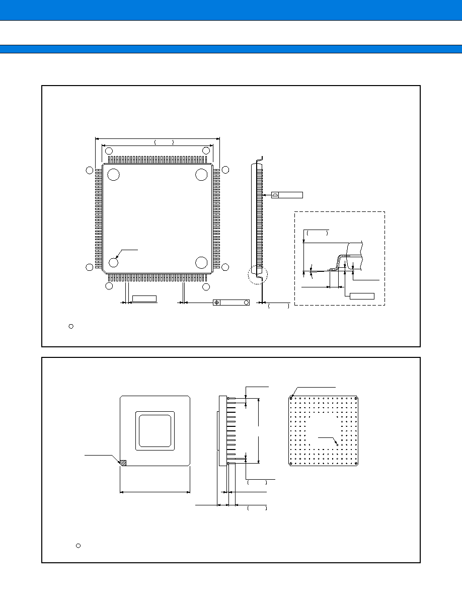
MB91301/MB91V301
112
s
PACKAGE DIMENSIONS
144-pin Plastic LQFP
(FPT-144P-M12)
Note 1) * : These dimensions include resin protrusion.
Resin protrusion is
+
0.25 (.010) Max (each side) .
Note 2) Pins width and pins thickness include plating thickness.
Note 3) Pins width do not include tie bar cutting remainder.
Dimensions in mm (inches)
179-pin Ceramic PGA
(PGA-179C-A03)
Dimensions in mm (inches)
C
2003 FUJITSU LIMITED F144024S-c-3-3
.059
≠.004
+.008
≠0.10
+0.20
1.50
Details of "A" part
0~8
∞
(Mounting height)
0.60±0.15
(.024±.006)
0.25(.010)
(.004±.002)
0.10±0.05
(Stand off)
0.08(.003)
0.145
≠0.03
+.002
≠.001
.006
+0.05
"A"
.007±.001
0.18±0.035
M
0.07(.003)
36
37
1
LEAD No.
0.40(.016)
INDEX
144
109
108
18.00±0.20(.709±.008)SQ
SQ
16.00
73
72
*
.630
≠.004
+.016
≠0.10
+0.40
C
1994 FUJITSU LIMITED R179004SC-3-2
INDEX AREA
6.10(.240)
MAX
1.27±0.25
.018
≠.002
+.007
≠0.05
+0.18
0.46
.134
≠.014
+.016
≠0.36
+0.41
3.40
1.27(.050)TYP DIA
35.56(1.400)
REF
INDEX
DIA
38.10±0.51
(1.500±.020)
(.050±.010)
SQ
2.54±0.25
(.100±.010)

MB91301/MB91V301
FUJITSU LIMITED
All Rights Reserved.
The contents of this document are subject to change without notice.
Customers are advised to consult with FUJITSU sales
representatives before ordering.
The information, such as descriptions of function and application
circuit examples, in this document are presented solely for the
purpose of reference to show examples of operations and uses of
Fujitsu semiconductor device; Fujitsu does not warrant proper
operation of the device with respect to use based on such
information. When you develop equipment incorporating the
device based on such information, you must assume any
responsibility arising out of such use of the information. Fujitsu
assumes no liability for any damages whatsoever arising out of
the use of the information.
Any information in this document, including descriptions of
function and schematic diagrams, shall not be construed as license
of the use or exercise of any intellectual property right, such as
patent right or copyright, or any other right of Fujitsu or any third
party or does Fujitsu warrant non-infringement of any third-party's
intellectual property right or other right by using such information.
Fujitsu assumes no liability for any infringement of the intellectual
property rights or other rights of third parties which would result
from the use of information contained herein.
The products described in this document are designed, developed
and manufactured as contemplated for general use, including
without limitation, ordinary industrial use, general office use,
personal use, and household use, but are not designed, developed
and manufactured as contemplated (1) for use accompanying fatal
risks or dangers that, unless extremely high safety is secured, could
have a serious effect to the public, and could lead directly to death,
personal injury, severe physical damage or other loss (i.e., nuclear
reaction control in nuclear facility, aircraft flight control, air traffic
control, mass transport control, medical life support system, missile
launch control in weapon system), or (2) for use requiring
extremely high reliability (i.e., submersible repeater and artificial
satellite).
Please note that Fujitsu will not be liable against you and/or any
third party for any claims or damages arising in connection with
above-mentioned uses of the products.
Any semiconductor devices have an inherent chance of failure. You
must protect against injury, damage or loss from such failures by
incorporating safety design measures into your facility and
equipment such as redundancy, fire protection, and prevention of
over-current levels and other abnormal operating conditions.
If any products described in this document represent goods or
technologies subject to certain restrictions on export under the
Foreign Exchange and Foreign Trade Law of Japan, the prior
authorization by Japanese government will be required for export
of those products from Japan.
F0302
©
FUJITSU LIMITED Printed in Japan