
Gemini Series, Page 1
Part No. 98≠004 Rev. 1.0
WWW.GALAXYPWR.COM
The Gemini Series is a high current three
quarter brick DC/DC converter with:
1.5 to 2.5 Volt, 55 Amp Output
3.3 or 5V Input Option
No Heat Sinking Required
4 Pin Programmable Output Voltage
87% Efficient: 3.3Vin and 2.5Vout @ 40A
84% Efficient: 5Vin and 2.5Vout @ 55A
137.5 Watts @ 100
∞ Baseplate
33 Watts/cu. inch
2.3" x 3" x 0.6"
Fixed Frequency Operation
Automatic OVP Tracking to Voltage Trim
Current Limiting with Auto≠Recovery
Power Good Signal
Two Year Warranty
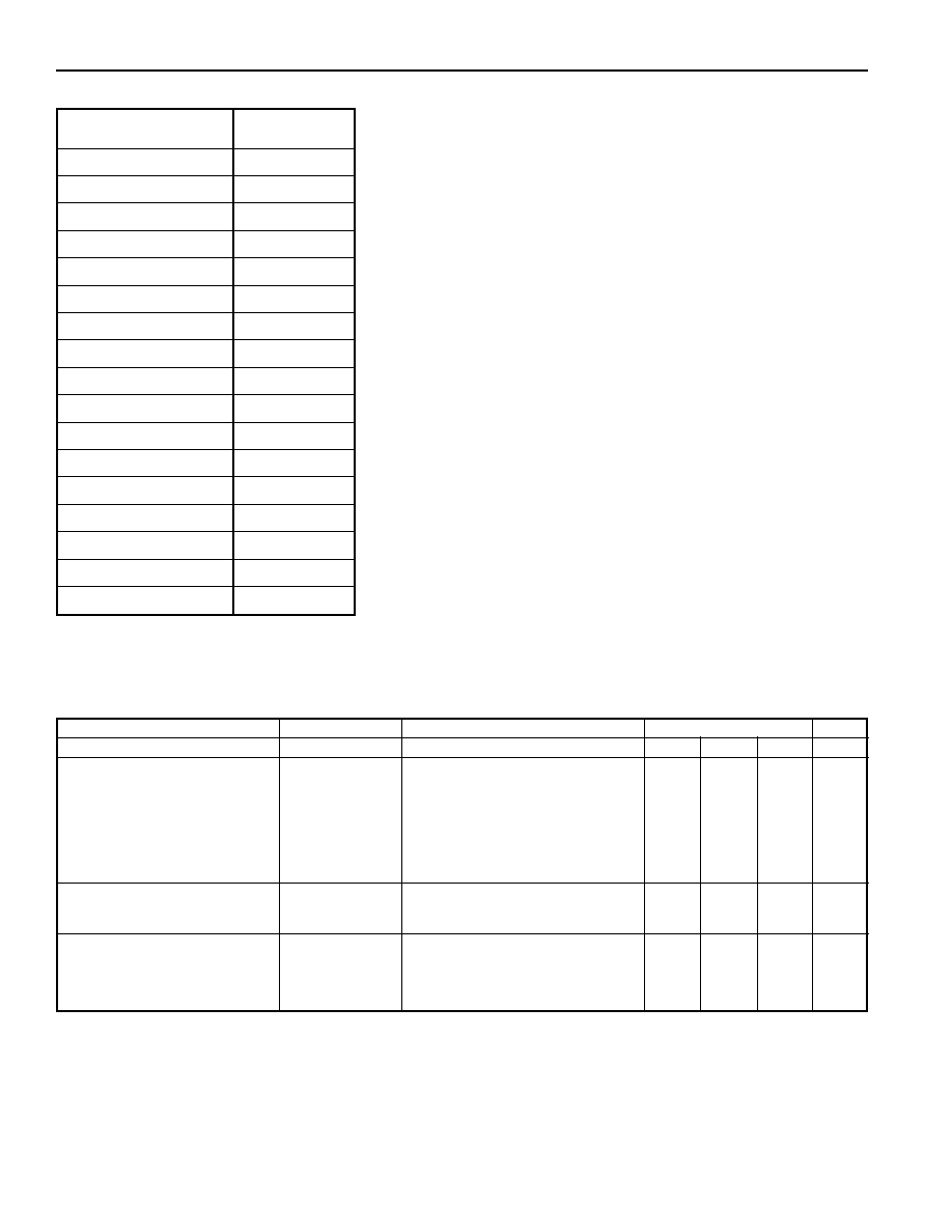
Gemini Series
Control Functions
Remote Sense
Output Enable
Protection Features
Over Temperature Protection
Over Voltage Protection
Over Current Protection
Typical Characteristics
Output Setpoint Accuracy:
±1%
Load & Line Regulation:
±0.5%
Total Regulation:
±5%
Noise & Ripple: 100 mVp≠p
Output Trim
DC/DC Converter Powers
600MHz Microprocessors

Gemini Series, Page 2
Part No. 98≠004 Rev. 1.0
WWW.GALAXYPWR.COM
Input Characteristics
Operating Air Temperatures from 0
∞C to +45∞C with 200 LFM, D
0
, D
1
, D
2
, D
3
pins low state unless otherwise specified.
Parameter
Test Condition
Requirement
Unit
Name
Var
Symbol
Min
Max
Input Voltage
3V3≠40
V
I
I
O
= 40A
3.37
3.8
V
≠S, ≠L
V
I
I
O
= 55A
4.5
5.25
V
Input Low Line Power-On V
V
I
on
Module Power On
≠
3.35
V
No Load Input Power
P
IL
V
I
=V
I
nom
≠
6
W
Input Capacitor
3V3≠40
20 (330
µF)
6600
≠
µF
(external to the converter)
≠S, ≠L
12 (330
µF)
3900
≠
µF
Input Current
3V3≠40
I
I
V
I
= 3.43V, I
O
= 40A, V
O
= 2.5V
≠
35.2
A
≠S, ≠L
I
I
V
I
= 5V, I
O
= 55A, V
O
= 2.5V
≠
35
A
Efficiency
3V3≠40
N
V
I
= 3.43V, I
O
= 40A, V
O
= 2.5V
83
≠
%
(with Local Sense)
≠S, ≠L
N
V
I
= 5V, I
O
= 55A, V
O
= 2.5V
79
≠
%
Reflected Input Ripple
3V3≠40
dI
I
V
I
= 3.43V, I
O
= 40A, (Note 1)
≠
6.0
A
P≠P
C
IN
= 20 (330
µF Tantalum)
ESR = 60 m
≠S, ≠ L
dI
I
V
I
= 5V, I
O
= 55A, (Note 1)
≠
11.0
A
P≠P
C
IN
= 12 (330
µF Tantalum)
ESR = 60 m
Switching Frequency
F
S
250 Typ
KHz
Note 1: Measure input reflected current which is drawn from input capacitor C
IN
by converter. Place 3" loop between C
IN
and V
IN
of the converter.
General Specifications
Operating Temperature
0
∞C to +45∞C (@200LFM)
Storage Temperature
≠20
∞C to +100∞C
Relative Humidity
10% to 95% RH,
Non≠condensing
Vibration
10≠500Hz 0.75g peak
Weight
75gm, typical (GPEV6≠3V3≠40)
200gm, typical (≠S, ≠L)
Material Flammability
UL94V≠0
MTBF
MIL≠HDBK≠217
1.2million hours*
* Note: 50% load; 200LFM, 45
∞C ambient
Specifications

Gemini Series, Page 3
Part No. 98≠004 Rev. 1.0
WWW.GALAXYPWR.COM
Output Characteristics
Over the complete baseplate temperatures and input voltage ranges, D
0
, D
1
, D
2
, D
3
pins low state unless otherwise specified.
Parameter
Test Condition
Requirement
Unit
Name
Var
Symbol
Min
Typ
Max
Output Voltage Set Point
3V3≠40
V
O
nom
V
I
= 3.43V, I
O
= 20A
2.475
2.500
2.525
V
≠S, ≠L
V
O
nom
V
I
= 5.0V, I
O
= 30A
2.475
2.500
2.525
V
Rated Output Current
3V3≠40
I
O
V
O
= V
O
nom
0
≠
40
A
≠S, ≠L
I
O
V
O
= V
O
nom
0
≠
55
A
Line & Load Regulation
3V3≠40
V
I
= 3.37≠3.8V, I
O
= 0≠40A
≠
≠
12.5
mV
≠S, ≠L
V
I
= 4.5≠5.25V, I
O
= 0≠55A
≠
≠
12.5
mV
Noise and Ripple
3V3≠40
V
I
= 3.43V, I
O
= 40A
≠
100
120
mV
P≠P
C
O
= 330
µF, 0.47µF
≠S, ≠L
V
I
= 5.0V, I
O
= 55A
≠
100
120
mV
P≠P
C
O
= 330
µF, 0.47µF
Total Regulation
3V3≠40
V
I
= 3.37≠3.8V, I
O
= 0≠40A
2.375
2.500
2.625
V
(Load, Line, Short term and
C
O
= 20 (470
µF)
Long term Dynamic
≠S, ≠L
V
I
= 4.5≠5.25V, I
O
= 0≠55A
2.375
2.500
2.625
V
Temp Drift)
C
O
= 20 (470
µF)
Remote Sense
V
I
= V
I
min, I
O
= full load
≠
≠
100
mV
Compensation Round Trip
Static Output Overvoltage
V
I
= V
I
nom
, I
O
= 5A
107
≠
120
%V
O
Protection (Nom) Latching
Output Voltage Protection
t
OVP
V
I
= V
I
nom
, I
O
= 5A
≠
≠
50
µS
Response Time
Current Limit (Nom)
3V3≠40
I
L
V
I
= 3.43V, V
O
= 2.5V
42
≠
≠
A
≠S, ≠L
I
L
V
I
= 5.0V, V
O
= 2.5V
57
≠
≠
A
Short Circuit Current
3V3≠40
I
SC
V
I
= 3.43V, V
O
< 0.6V
≠
≠
55
Arms
≠S, ≠L
I
SC
V
I
= 5.0V, V
O
< 0.6V
≠
≠
70
Arms
Over≠temperature
≠
110
125
∞C
Shutdown (T
baseplate
)
Load Transient Response,
V
OPK
I
O
= 10≠38A @ 28A
µS (di/dt)
≠
≠
3
%V
O
V
O
deviation from steady
Notes
V
I
= 3.3V(3V3-40)
state (settling time to
±1%)
1, 2, 3
V
I
= 5.0V(≠S, ≠L)
V
O
= 2.5V pos. or neg. step
C
O
= 28≠470
µF Cap
≠
≠
1200
µS
(470
µF, ESR=55m)
C
IN
=12≠330
µF Cap
(330
µF, ESR=60m)
Turn≠on Time
t
on
V
I
=V
I
min
to V
I
max,
I
O
=0≠40A
20
≠
120
mS
(See figures on page 5)
Turn≠on Risetime (10≠90%)
t
rise
8
≠
30
mS
Output Filter Capacitance
C
out
V
I
=5.0V, I
O
=I
O
max
330
13,200
µF
Voltage Trim
V
trim
V
I
=V
Inom
, I
O
=I
O
max/2
94.5
95.5
96.5 %V
O
nom
V
O
=2.5V, Short Pin 1 & 10
Notes: 1. The converter output voltage shall be stable when (13,200
µF total) tantalum low ESR filter capacitors are connected across the output of the converter.
2. For 3.43 Input Voltage Rail having I
O
max = 40A, the minimum input filter capacitor required is 6600
µF (use multiple 330µF tantalum capacitor having 60m ESR.)
3. For 5.00 Input Voltage Rail having I
O
max = 55A, the minimum input filter capacitor required is 3960
µF (use multiple 330µF tantalum capacitor having 60m ESR.)
Specifications
Gemini Series, Page 4
Part No. 98≠004 Rev. 1.0
WWW.GALAXYPWR.COM
Specifications
Output Voltage Adjustments
Control Pin
Output Voltage
Tolerance
±1.2%
D
3
D
2
D
1
D
0
Volts DC
1
1
1
1
1.429
1
1
1
0
1.500
1
1
0
1
1.571
1
1
0
0
1.643
1
0
1
1
1.714
1
0
1
0
1.786
1
0
0
1
1.857
1
0
0
0
1.929
0
1
1
1
2.000
0
1
1
0
2.071
0
1
0
1
2.143
0
1
0
0
2.214
0
0
1
1
2.286
0
0
1
0
2.357
0
0
0
1
2.429
0
0
0
0
2.500
Note: the converter shall be tested for four bits logic control.
Control Signal Characteristics
D
0
, D
1
, D
2
, D
3
pins low state unless otherwise specified.
Parameter
Test Condition
Requirement
Unit
Name
Symbol
Min
Typ
Max
Enable_H*
V
I
= V
I
nom
, I
O
= 20A
Enable_H Source Current
≠
≠
1.0
mA
Enable_H Voltage Low
≠
≠
0.8
V
Enable_H Voltage High
4.5
≠
5.2
V
Enable_H High (Output Voltage)
2.475
2.500
2.525
V
Powergood_H High
V
I
= V
I
nom
, I
O
= 20A
3.3
≠
≠
V
Powergood_H Low
V
S
≠ 5.0V, R
L
= 4K
≠
≠
0.8
V
Fault_H High
V
I
= V
I
nom
4.0
≠
5.1
V
Fault_H Low
R
L
= 4K
TO
≠S
ENSE
≠
≠
0.8
V
Fault_H Source Current
1
≠
≠
mA
* Use Open Collector Logic to control Enable function.

Gemini Series, Page 5
Part No. 98≠004 Rev. 1.0
WWW.GALAXYPWR.COM
Control Signals
Control Signal Characteristics: Per Table on Page 4.
Enable_H: This input signal is used to enable the output of the
converter when activated (active High). The signal is referenced to
either the output side (-Sense) or GND. It has an internal pull-up
resistor. To disable the converter requires an open collector logic
signal to pull it down.
4 Bit Logic Signals: The state of the 4 bit control signals controls
the output voltage. Normally, the 4 bits are in a `low state' and
provide for a 2.5V output voltage. The output voltage may be
programmed between 1.429 to 2.5V by setting appropriate logic
bits `high' through D0, D1, D2, and D3.
Powergood_H: The Powergood signal is in a `high' state when the
output voltage is within +/- 7.5% of the output voltage programmed
by the 4 logic bit inputs.
OVPFault_H: This signal is in a `high' state when the output
voltage is greater than +/-15% of the output voltage programmed by
the 4 bit logic inputs or exceeds the maximum operating
temperature of the converter. This output is the open emitter of a
transistor which pulls to +5V in the high state and is open in the
low state. For driving logic, an appropriate pull down resistor from
OVPFault_H to ≠ Sense is required. The OVPFault_H is asserted
high when OVPFault is activated. When driving an SCR to `crow-
bar' the input source from a Fault_H signal, use the circuit below:
Application Notes
Trim: The output voltage may be lowered from the nominal
programmed value by adding an external resistor from the TRIM
pin (J1-10) to ≠ Sense (J1-1). This is used to obtain output voltages
between the programmed values. The maximum value the output
may be trimmed is approximately ≠4.5% of Vprog. The resistor
value may be calculated from the following formula:
(2490) (Vtrim)
Rext = ≠≠≠≠≠≠≠≠≠≠≠≠≠≠≠≠≠≠≠ - 15000
(3.49) (Vprog ≠ Vtrim)
Vtrim = Desired output voltage with Rext tied from TRIM pin to
≠ SENSE.
Vprog = Nominal programmed output voltage
Notes: 1. Vtrim must be less than Vprog.
2. The trim pin does not change the OVP or Powergood_H trip
points. These are set by the 4 bit logic inputs
Enable Circuit Turn On Time
2N2222
100
0.
µ
1F
SCR
Fault_H
1K
+5V
2N7000
or
Equivalent
OFF >3V
ON
0.6V
ON/OFF
Gate Drive
Voltage
To (≠)
To V
ENABLE
Pin
220K
Gate Drive
Voltage
4.5V
0.8V
Falltime <1
µ
sec
TURN_ON
Time
V
OUT
90%
10%
Trise
Time
V
O
J1-J7
PowerGood_H
(Volt)
5.0V
PowerGood_H
Time
V
O
J1≠J10
Trim Pin
10V
0V
2.5V
Time
V
nom
t
OVP
Time
2.5V
V
nom
J1-J9
OVPfault_H
5.0V
OVPfault_H
Time
10V
V
OUT
0
Turn On Time
3.37-5.25V
Input
Output
20 (330
µ
F)
C=6600
µ
F
C=(20)470
µ
F
Tantalum Capacitors
9400
µ
F
+
R
LOAD
=40A
Output Load Conditions (Turn On)

Gemini Series, Page 6
Part No. 98≠004 Rev. 1.0
WWW.GALAXYPWR.COM
Package Detail
Pin Assignments
Power Pins (60 mils)
Pin
Designation
P1
Vin
P2
Vin
P3
Vin
P4
Vin
P5
Vin RTN
P6
Vin RTN
P7
Vin RTN
P8
Vin RTN
P9
Vo
P10
Vo
P11
Vo
P12
Vo
P13
Vo RTN
P14
Vo RTN
P15
Vo RTN
P16
Vo RTN
Signal Pins (25 mils sq.)
Pin
Designation
J1-1
-Sense
J1-2
+Sense
J1-3
D0
J1-4
D1
J1-5
D2
J1-6
D3
J1-7
PowerGood_H
J1-8
Enable_H
J1-9
OVPFault_H
J1-10
Trim
control
board
control
pins
2.300 Max
control
pins
P9
P1
P8
P16
3.025
Max
V
IN
RTN
+V
IN
V
O
RTN
+V
O
10 2
9 1
standoff/insert
max dia = 0.225"
0.300 min recommenced
clearance area around standoff
0.190 +/-0.020
0.300 min
0.025
0.025
0.052 max
0.145 +/-0.02
standoff to power pins
airflow direction
-S version only
Notes: 1. GPEV6-3V3-40 only: No heatsink, max height = 0.52"
2. Variations -S, -L only: 0.88" heatsink attached to plate.
Max height w/ heatsink =1.4"
3. Components on side 2 shall be 0.030" min. below the standoff.
Aluminum plate
flatness = 0.001 in/in
A
A
Bottom View (facing pins)
Side View
2.300 Max
control
pins
P9
P1
3.025
Max
1
0.162
Notes: Standoff is used for mounting the heatsink
on the plate of the converter. Use 4 - 40 screws.
Control pins: 0.025 sq pin, 2x 10 pos.
Power pins: 0.060 +/- 0.005 diameter
1.605
0.595
0.100
PCB
control board
Power Pins
0.150 ctr-ctr
Power Pins
0.200 ctr-ctr
2.000 ctr-ctr
0.050 Max
2 plcs
0.025 Max
2 plcs
2. 812
0.100
standoff
2.025
1.425
0.150
0.475
1.450
1.725
2.100
optional
insert
2.737
Bottom View (facing pins)
COnfiguration/Dimensions

Gemini Series, Page 7
Part No. 98≠004 Rev. 1.0
WWW.GALAXYPWR.COM
PACKAGE DETAIL
ORDERING INFORMATION
Model
Input
Output
Max
Efficiency
Number
Voltage
Voltage
Current
(Typ)
GPEV6-3V3-40
3.3≠5.25V
2.5 V
40 A
87 %
GPEV6-5V0-55-S*
4.5≠5.25 V
2.5 V
55 A
84%
GPEV6-5V0-55-L*
4.5≠5.25V
2.5 V
55 A
84%
* ≠S: short heatsink fins (perpendicular to long side)
≠L: long heatsink fins (parallel to long side)
2.650
0.163
1.130
0.120
2.975
0.475
1.250
4x
0.300
0.150
0.040
11x
0.196
2.200
13x
0.88
4x ÿ 0.160
Note: Recommended fin spacing
4x ÿ 0.160
2.200
0.163
2.650
1.130
0.475
0.120
0.120
2x 0.040
15x 0.050
14x 0.171
0.293
0.88
0.150
2.975
Note: Recommended fin spacing
Heatsink Variations
Fins Parallel to Long Side (≠L)
Fins Perpendicular to Long Side (≠S)

Gemini Series, Page 8
Part No. 98≠004 Rev. 1.0
WWW.GALAXYPWR.COM
155 Flanders Road Westborough, MA 01581
508≠870≠9775 Fax: 508≠870≠9796
e≠mail: galaxy@galaxypwr.com
website: http://www.galaxypwr.com
© Copyright 2000 Galaxy Power. Specifications subject to change without notice.
Galaxy Power Inc. warrants to the original purchaser that the products conform to this data sheet and are free from
material and workmanship defects for a period of two (2) years from the date of manufacture, if this product is used within
specified conditions. Galaxy Power Inc. reserves the right to make changes to the product(s) or information contained
herein without notice. No liability is assumed as a result of their use or application. No rights under any patent accompany
the sale of any such products or information. For additional details on this limited warranty consult the factory.