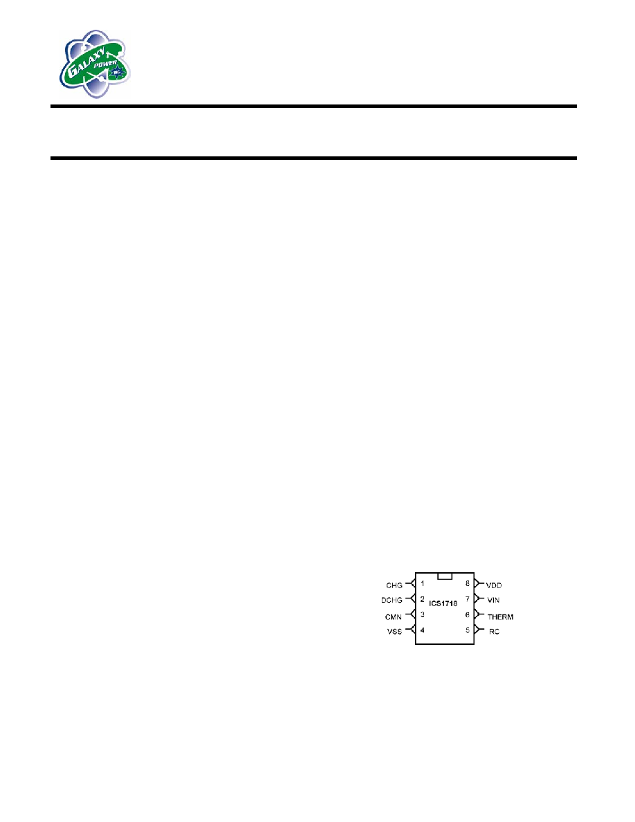
ICS1718
Galaxy
Power
Incorporated
QuickSaver
Pulse Conditioning
Charge Control IC for NiMH and NiCd Batteries
Features
Ideal for embedded NiMH/NiCd designs
13 bit ADC for precision sensing
Cost effective for charger stand designs
Termination methods
Voltage slope (+
V
/dt and +/- peak detect)
Fast charge time out to topping mode
Optional over temperature shutdown
Overvoltage shutdown
Four stage charge sequence
SoftStart conditioning
Fast charge
Topping charge
Maintenance charge
Four (4) standard user selectable charge rates
15 minutes (4C)
30 minutes (2C)
60 minutes (1C)
120 minutes (C/2)
16 bit RISC processor
Packaging: 8 pin SOIC, 8 pin DIP
Benefits
-compared to other methods
Peak battery performance and extended service
Improved battery efficiency and reliability
Lowest internal resistance build-up
Lowest capacity fade acceleration
Lowest battery self discharge rate
Applications
Embedded and charger stands
Portable consumer products
Power tools
Audio/video products
Communications products/RC toys
Wireless products
Description
The ICS1718 is a low cost 8 pin CMOS control IC
designed for the intelligent charging of nickel-
cadmium (NiCd) and nickel-metal hydride (NiMH)
batteries. The ICS1718 has four (4) user selectable
charge rates, user accessible clock, thermistor or
temperature switch input, and a charge status output
pin. The ICS1718 uses pulsed-current, with an
optional conditioning technique, and voltage slope
methods for a complete recharge without
overcharging, irrespective of the charge state of the
battery at the start of its charge. A brief polling
mode during the first moments after powerup
provides overvoltage protection from missing or
open batteries. When a battery is detected, charge
current is gradually increased up to the fast charge
level during a soft-start conditioning stage. A two
stage maintenance charge provides an opportunity
to further optimize the charge level in the battery.
The ICS1718 is ideal for applications where battery
temperature protection is required in the charger.
Charge rates are user selected. Four different
standard charge times between 15 minutes (4C) and
two hours (C/2) are available. The ICS1718 has
options to prevent charging at temperatures above a
designer set maximum as well as low current charge
at battery temperatures below a designer set
minimum. Internal maximum and minimum voltage
thresholds provide over/under voltage shutdown
protection.
ICS1718
2
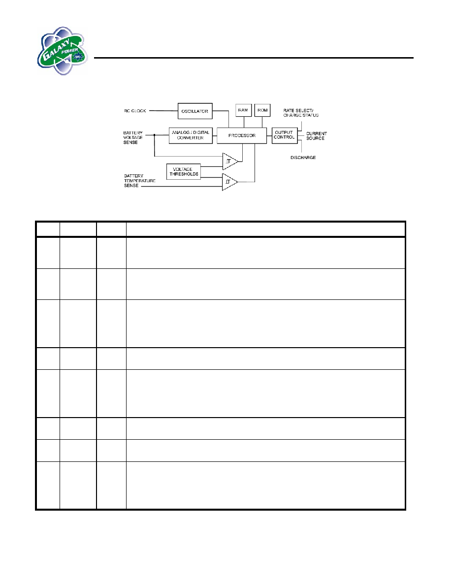
Block Diagram
Pin Descriptions
Pin Name Type
Description
1 CHG OUT
Active high (PFET), active low (NFET) 16
, 25mA max., TTL compatible signal.
High (5V) turns on and a low (0V) turns off an external current limited voltage
regulated charging source to provide pulse charge to the battery.
2 DCHG OUT
Active high (PFET), active low (NFET) 16
, 25mA max., TTL compatible signal.
High (5V) turns on and a low (0V) turns off an external transistor to sink a
conditioning pulse discharge current from the battery using an external resistor.
3 CMN OUT
Charge mode indicator. NFET drain rated 10
, 40mA max. Goes low to turn on
external indicator showing battery is in soft start/fast charge. Alternately goes low
and off (open) at a 0.5 or 1Hz rate to show battery is ready as
topping/maintenance charges are applied. Off (open) with 5V VDD indicates over-
voltage/temp shutdown and/or missing battery.
4 VSS PWR
Ground that connects directly to a solid (low impedance) ground at or close to
battery minus.
5 RC IN
An external resistor from this pin to VDD and an external capacitor from this pin to
VSS set the frequency of the internal oscillator, providing the clock for the device.
15K
or 30K and 100pF are normally used. Pin 5 can be driven by a 500KHz or
by a 1 MHz external 0 to 5V rectangular pulse with duty cycle 10 to 60 %, capable
of supplying 7 mA.
6 THERM IN Thermistor or thermal switch input referenced to battery negative provides battery
temperature sensing. If not used, connect to ground.
7 VIN IN
Battery voltage is divided down with an external resistor divider for ending fast
charge also sets back-up over-voltage and under-voltage shutdown limits.
8 VDD PWR
Device supply = Series regulated 5.0 VDC +/- 10%, 50mA. The ICS1718
maximum average (8.25mA) includes brief 50mA peak currents. When used,
LEDs, pull-up resistors, and drivers also require current from the +5VDC supply. A
.01uF or larger ceramic capacitor between (and close to) VDD and VSS is used for
bypassing, in addition to the output capacitor required by the regulator.
Input and output pins all have internal ESD protection diodes to VDD and VSS for 2KV protection per MIL STD 883 method 3015.7.
Depending on the application, set-up, board layout, etc. additional ESD protection may be required.

ICS1718
3
Charging Stages
The normal charging sequence consists of four stages. The application of current is shown graphically in Fig. 1.
The soft-start charge stage gradually increases during the first two or four minutes of charge depending on the
charge rate selected. The soft-start is followed by a near full duty cycle, constant amplitude current charge, which
continues until termination. After termination, either a two hour or four hour topping charge, depending on the
charge rate selected, is applied, followed by a maintenance charge.
Fig. 1: Graphical representation of current levels during the four charging stages.
Stage 1: Soft-Start Charge
New, overdischarged, and batteries out of long term storage may exhibit a high impedance condition initially. The
high impedance causes a voltage spike at the beginning of the charge cycle as shown in Fig. 2.
Fig. 2: High impedance voltage spike at the beginning of charge.

ICS1718
4
The voltage-time integral of the voltage spike remains constant regardless of the charge rate. At higher charge
rates the amplitude of the spike is relatively high, but the time duration is short. At lower charge rates, the
amplitude of the spike is less but the time duration is proportionally longer. Unless remedied the spike might be
misinterpreted as a fully charged battery by a voltage slope termination method. So the soft-start charge is
applied to ease the battery into fast charge by gradually increasing the duty cycle of the charge from 20% to
nearly 100% the first two or four minutes of charge. The gradual increase in duty cycle alleviates the high
impedance condition before fast charge stage begins. The applied current is raised to the desired fast charge
duty cycle by extending the charge pulse width on every cycle until the current is applied for the entire fast charge
pulse width (t
CPW
), as shown in Fig. 3. The initial pulse width (t
IPW
) is approximately 1/5
th
of the fast charge pulse
width. The soft-start pulse width increases by t
inc
over 120 cycles that is determined by
t
t
t
inc
CPW
IPW
=
-
120
.
The cycle time, denoted by t
cycle
in Fig. 3, is slightly longer than the fast charge pulse width. The timing
relationship of the charge pulse to the cycle time is shown in Fig. 4. The charge indicator (CMN) is active low
during this stage.
Fig. 3: Cycle to cycle increase of the soft-start current pulse widths.
Stage 2: Fast Charge
The ICS1718 applies the charge current in a repetitive sequence consisting of charge and optional discharge
pulses with rest times throughout the fast charge. The pulsed conditioning technique consists of a relatively long
charging pulse followed by a brief discharge pulse. The cycle, shown with charge, discharge, rest and data
acquisition periods in Fig. 4, repeats until the battery is fully charged.
Fig. 4: Charge cycle showing charge and discharge current pulses.
The conditioning discharge pulse amplitude is normally set at 2.5 times the amplitude of the actual charging
current based on 1.4V/cell. Setting the discharge pulse to the same amplitude as the charge current still provides
some conditioning. Not using the discharge pulse conditioning option will not affect the operation of the ICS1718.

ICS1718
5
The discharge pulse width is typically 5ms every 1.1 seconds for the 4C and 1C rates (and 10ms every 2.2
seconds for the 2C and C/2 rates), so the external transistor and resistor selected for accomplishing the discharge
pulse are determined using conservative pulse ratings. The duty cycle of the reverse pulse is 0.5% maximum of
the fast charge duty cycle. Since the discharge current is rectangular, the RMS current in the resistor and
transistor (logic NFET, high gain NPN, or NPN Arlington) is equal to the peak current times the square root of the
duty cycle. So the RMS heating effect current is about 7% of the discharge current peak amplitude. Using
conservative pulsed, rather than steady-state ratings, for selecting the discharge resistor and transistor results in
relatively small, low cost devices.
An ADC acquisition window for measuring battery voltage immediately follows a brief rest time after the
conditioning discharge pulse. No current is applied during the rest time or the window to allow the battery voltage
to stabilize. Since no current is flowing, the measured voltage is not obscured by any internal or external drops
and distortions caused by current flow and battery surface charge. The ICS1718 takes one voltage reading of the
quiet time battery voltage during the acquisition window. Voltage slope calculations using voltages measured
during this window provides the most accurate representation of the relative state of charge of the battery.
Stage 3: Topping Charge
The topping charge stage applies current at a duty cycle that provides cell equalization in multiple cell packs.
When the ICS1718 completes the fast charge, the battery is ready to use as the CMN indicator alternates ON and
OFF at a 1 or 2 second rate. If charging is allowed to continue, the topping charge is applied for a minimum of
two or four hours, depending on the charge rate selected. The charging current consists of the same pulsed
current technique used during fast charge, however a delay time is introduced as shown in Fig. 5. Extending the
delay time between charge pulses allows the use of the same amplitude current used in fast charge so no altering
of the current source is required.
Fig. 5: Representative timing diagram for topping and maintenance charges.
Stage 4: Maintenance Charge
The maintenance charge offsets the natural self-discharge of NiCd or NiMH batteries keeping the battery primed
at peak charge. After topping ends, the ICS1718 begins maintenance by once again extending the duty cycle of
the applied current pulses. The topping charge delay is increased by a factor of four and continues for as long as
a battery voltage is present at the voltage sense (VIN) pin. As in the topping charge, the charge mode indicator
(CMN) alternates on and off at a one or two second rate, depending on the charge rate selected.
Cold Battery Temperature Charge
The efficiency of the oxygen-recombination reaction in NiCd or NiMH cell is lower at cold temperatures. To reduce
the pressure generated by hydrogen gas at the negative electrode, the ICS1718 provides an option to charge at
the topping rate until the battery warms up. Cold temperature charging is activated if a voltage at the temperature
sense (THERM) pin is in the cold temperature voltage range as shown in Table 4A and Figure 9. The voltage at
THERM pin 6 is produced by a NTC thermistor in the battery pack. A series resistor to THERM pin 6 and an
external pull-up resistor to +5V (VDD) in the charge circuit are used to set cold battery charging. The ICS1718
only checks for a cold battery prior to the start of fast charge.
If a cold battery is detected prior to fast charge, the ICS1718 applies the topping charge. The charge mode
indicator (CMN) alternates on and off, indicating that a low current charge is being applied to the cold battery.
The voltage at THERM pin 6 is monitored continually to see if the battery has warmed. If so, the ICS1718 quits
the topping charge and begins a fast charge at the rate selected starting with soft start.