This document contains information that describes this design as completely as possible at the time of this revision. Some or
all of this information may be deemed confidential and should not be released without a non-disclosure agreement. Data and
specification characterizations are in process and may be changed in subsequent releases.
GPI Internal Information Only
Revision 2.1 - March 19, 2003
QSC1702-MOT 68HRC05
QuickSaver
Battery Charge Control Software Core for
Motorola's 8-bit 68HRC705JJ7/JJ6 Microcontrollers
Standard Features
Ideal for embedded NiMH/NiCd designs
12 bit ADC
Cost effective for charger stand designs
External resistor set oscillator
Termination methods
Voltage slope (+
V
/dt and +/- peak detect)
Fast charge time out to maintenance mode
Hot/cold battery charge current removal with
hysteresis in fast charge stage
Pre-fast charge stage modes
Cold battery warm-up charge
Hot battery charge hold-off
Four stage charge sequence
SoftStart conditioning
Fast charge
Topping charge
Maintenance charge
Standard charge rates
60 minutes (1C)
120 minutes (C/2)
Packaging: 20 pin SOIC, 20 pin DIP
Benefits
-compared to other methods
Peak battery performance and extended service
Improved battery efficiency and reliability
Lowest internal resistance build-up
Lowest capacity fade acceleration
Lowest battery self discharge rate
Applications
Embedded and charger stands
Portable consumer products
Power tools
Audio/video products
Communications products
RC toys
Wireless products
Battery analyzers
Description
The QuickSaver
software core QSC1702 is a
flexible, low cost offering for porting to the Motorola
family of 8-bit microcontrollers, allowing swift time to
market with the exact customer feature set required.
The QSC1702 core includes all the patented
functions that are available in the ICS17XX ICs, and
ample code space for feature set code
modifications. The core is optimization for the
intelligent charging of nickel-cadmium (NiCd) and
nickel-metal hydride (NiMH) batteries, including
options for Li-Ion and Li-Polymer. The standard
core offers two (2) programmed charge rates,
thermistor input, and status outputs. The core uses
a pulsed-current conditioning technique and voltage
slope, and/or temperature slope, methods for a
complete recharge without overcharging,
irrespective of the charge state of the battery at the
start of its charge. A brief polling mode during the
first moments after powerup provides battery
detection, and advanced diagnostics. Charge
current is gradually increased up to the fast charge
level during a soft-start conditioning stage. A two
stage maintenance charge provides an opportunity
to further optimize the charge level in the battery.
The standard core delays the start of fast charge for
temperatures above a designer set maximum and
applies a low current charge for battery
temperatures below a designer set minimum.
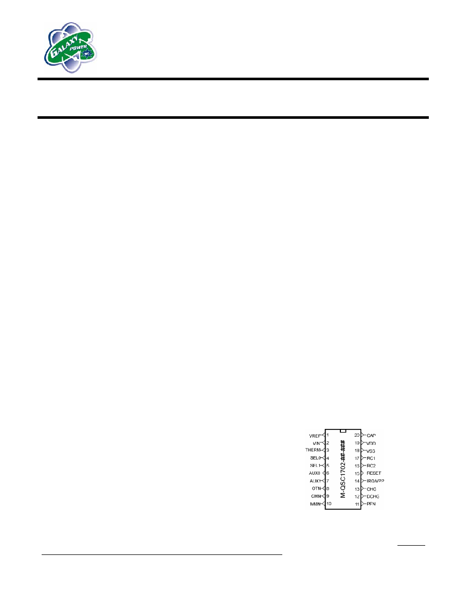
Pin Configuration

QSC1702-MOT 68HC05
2
Pin Definitions
Pin Name Type
Description
1 VREF IN
External
resistor
divider
from 5V provides a 1V reference.
2
VIN
IN
Battery voltage is divided down with an external resistor divider for ending fast charge.
3
THERM
IN
Thermistor voltage is from an external pull-up resistor to 5V provides for temperature slope termination
and hot or cold battery detection.
4
SEL0
IN
H = 1C (1 hour rate); L = C/2 (2 hour rate).
5 SEL1 IN
{Spare}
6
AUX0
IN
H = Normal fast charge; L = Discharge battery to 1V/cell.
7 AUX1 IN
{Spare}
8
OTN
OUT
Out of temperature range mode indicator. Goes low to turn on external indicator showing battery cold.
Alternately goes low and off (open) at a 1Hz rate to show battery is hot.
9
CMN
OUT
Charge mode indicator. Goes low to turn on external indicator showing battery is in soft start/fast
charge.
10
MMN
OUT
Maintenance mode indicator. Goes low to turn on external indicator showing battery is charged and
ready to use. Alternately goes low and off (open) at a 1Hz rate to show battery too cold to fast charge
or topping/maintenance charge pulses are applied. Outputs diagnostic data while fast charge is in
progress. Blinks to indicate discharge only.
11
PFN
OUT
Polling mode indicator. Goes low to turn on external indicator showing battery is missing or open.
Alternately goes low and off (open) at a 1Hz rate to show battery voltage is lower than normal as fast
charge continues. When charge completes (MMN low) PFN blinks at 1Hz to indicate shorted cells.
12
DCHG
OUT
Active high (PFET), active low (NFET), TTL compatible signal. High (5V) turns on and a low (0V) turns
off an external transistor to sink a conditioning pulse discharge current from the battery using an
external resistor, or constant current discharge circuit. Also used to discharge the battery using the
conditioning pulse circuit.
13
CHG
OUT
Active high (PFET), active low (NFET), TTL compatible signal. High (5V) turns on and a low (0V) turns
off an external current limited charging source to provide charge to the battery.
14
IRQ/Vpp
An interrupt signal on the IRQ/Vpp pin latches an external interrupt request.
15
RESET
IN
A low resets the MCU.
16
RC2
IN
Input for one side of timing resistor or external oscillator
17
RC1
IN
Input for one side of timing resistor or external oscillator
18
VSS
GND
Ground that connects directly to a solid (low impedance) ground at or close to battery minus
19
VDD
PWR
Device supply = Series regulated 5.0 VDC +/- 10%, 100mA. The QSC1702-MOT 68HRC05 maximum
average includes brief 50mA peak currents. When used, LEDs, pull-up resistors, and drivers require
additional current from the +5VDC supply that should not exceed 50mA when using a 100mA regulator.
A .01uF or larger ceramic capacitor between (and close to) VDD and VSS is used for bypassing, in
addition to the output capacitor required by the regulator.
20
CAP
IN
A .94uF (two .47uF in parallel) external capacitor for A/D sampling.
Input and output pins all have internal ESD protection diodes to VDD and VSS for 2KV protection per MIL STD 883 method 3015.7.
Depending on the application,set-up, board layout, etc. additonal ESD protection may be required.
GPI Internal Information Only
Revision 2.1 - March 19, 2003
QSC1702-MOT 68HC05
Controller Operations
Charging Stages
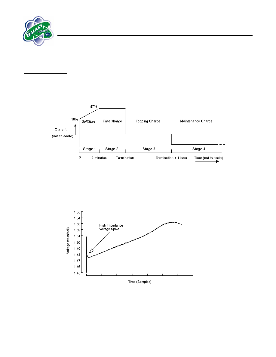
The normal charging sequence consists of four stages. The application of current is shown graphically in Fig. 1.
The soft-start charge stage gradually increases during the first two minutes of charge. The soft-start is followed by
a near full duty cycle constant amplitude current charge, which continues until termination. After termination, a
one hour topping charge is applied, followed by a maintenance charge.
Fig. 1: Graphical representation of current levels during the four charging stages.
Stage 1: Soft-Start Charge
New, overdischarged, and batteries out of long term storage may exhibit a high impedance condition initially. The
high impedance causes a voltage spike at the beginning of the charge cycle as shown in Fig. 2.
Fig. 2: High impedance voltage spike at the beginning of charge.
GPI Internal Information Only
Revision 2.1 - March 19, 2003
QSC1702-MOT HC6805
The voltage-time integral of the voltage spike remains constant regardless of the charge rate. At higher charge
rates the amplitude of the spike is relatively high, but the time duration is short. At lower charge rates, the
amplitude of the spike is less but the time duration is proportionally longer. Unless remedied the spike might be
misinterpreted as a fully charged battery by a voltage slope termination method. So the soft-start charge is
applied to ease the battery into fast charge by gradually increasing the duty cycle of the charge from 20% to
nearly 100% the first minutes of charge. The gradual increase in duty cycle alleviates the high impedance
condition before fast charge stage begins. The applied current is raised to the desired fast charge duty cycle by
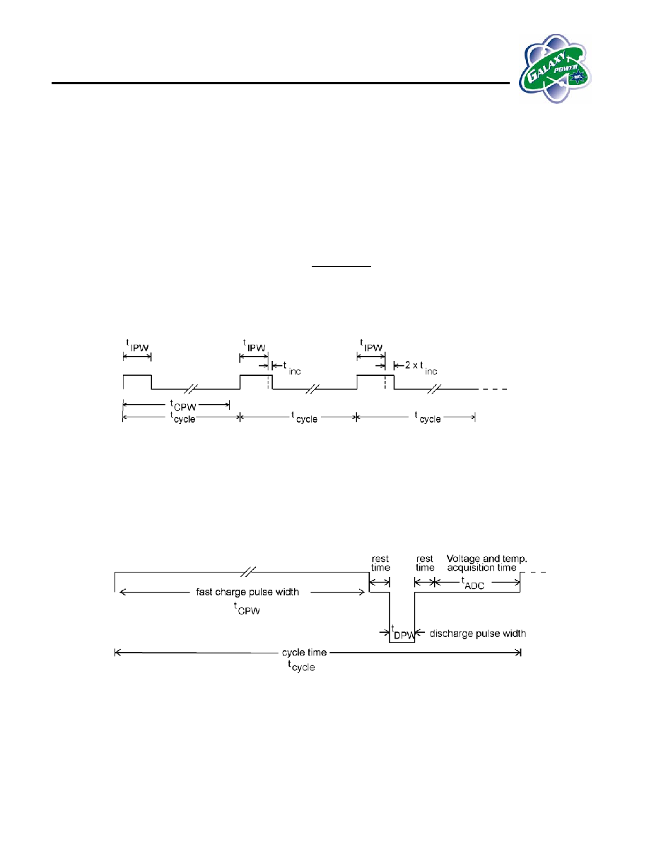
extending the charge pulse width on every cycle until the current is applied for the entire fast charge pulse width
(t
CPW
), as shown in Fig. 3. The initial pulse width (t
IPW
) is approximately 1/5
th
of the fast charge pulse width. The
soft-start pulse width increases by t
inc
over 120 cycles that is determined by
t
t
t
inc
CPW
IPW
=
-
120
.
The cycle time, denoted by t
cycle
in Fig. 3, is slightly longer than the fast charge pulse width. The timing
relationship of the charge pulse to the cycle time is shown in Fig. 4. The charge indicator (CMN) is active low
during this stage.
Fig. 3: Cycle to cycle increase of the soft-start current pulse widths.
Stage 2: Fast Charge
The QSC1702-MOT 68HRC05 applies the charge current in a repetitive sequence consisting of charge and
discharge pulses with rest times throughout the fast charge. The pulsed conditioning technique consists of a
relatively long charging pulse followed by a very short high current discharge pulse. The cycle, shown with
charge, discharge, rest and data acquisition periods in Fig. 4, repeats until the battery is fully charged.
Fig. 4: Charge cycle showing charge and discharge current pulses.
The conditioning discharge pulse amplitude is normally set at 2.5 times the amplitude of the actual charging
current based on 1.4V/cell for both NiMH and NiCd batteries. Setting the discharge pulse to the same amplitude
as the charge current still provides some conditioning.
GPI Internal Information Only
Revision 2.1 - March 19, 2003
QSC1702-MOT 68HC05
The discharge pulse width is typically 5ms every 1.1 seconds, so the external transistor and resistor selected for
accomplishing the discharge pulse are determined using conservative pulse ratings. The duty cycle of the reverse
pulse is 0.5% maximum of the fast charge duty cycle. Since the discharge current is rectangular, the RMS current
in the resistor and transistor (logic NFET, high gain NPN, or NPN darlington) is equal to the peak current times
the square root of the duty cycle. So the RMS heating effect current is about 7% of the discharge current peak
amplitude. Using conservative pulsed, rather than steady-state ratings, for selecting the discharge resistor and
transistor results in relatively small, low cost devices.
An ADC acquisition window for measuring the cell voltage and/or temperature (as options) immediately follows a
brief rest time after the conditioning discharge pulse. No current is applied during the rest time or the window to
allow the battery voltage to stabilize, and thermistor voltage to be unobstructed by external voltage drops and
noise. Since no current is flowing, the measured battery voltage is not obscured by any internal or external drops
and distortions after by surface charge has been removed. The QSC1702-MOT 68HRC05 takes one voltage
reading of the quiet time battery voltage, and as an option thermistor voltage, during the acquisition window. The
measurements during this window provide a most accurate representation of the true state of charge of the
battery and its temperature.
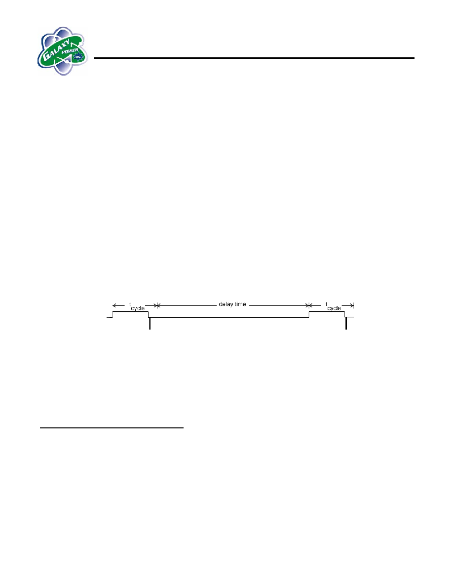
Stage 3: Topping Charge
The topping charge stage applies current at a duty cycle that provides cell equalization in multiple cell packs.
When the QSC1702-MOT 68HRC05 completes the fast charge, the battery is ready to use as signaled by the
MMN. If charging is allowed to continue, the topping charge is, it consists of the same pulsed current technique
used during fast charge, however a delay time is introduced as shown in Fig. 5. Extending the delay time
between charge pulses allows the use of the same amplitude current used in fast charge so no altering of the
current source is required.
Fig. 5: Representative timing diagram for topping and maintenance charges.
Stage 4: Maintenance Charge
The maintenance charge offsets the natural self-discharge of NiCd or NiMH batteries keeping the battery primed
at peak charge. After topping ends, the QSC1702-MOT 68HRC05 begins maintenance by once again extending
the duty cycle of the applied current pulses. The topping charge delay is typically increased by a factor of four and
continues for as long as a battery voltage is present at the voltage sense (VIN) pin. As in the topping charge, the
the ready state of the battery continues to be signalled by the MMN indicator.
Fast Charge Termination Methods
Three main fast charge termination methods are used: positive voltage slope (
V/t) and +/- peak voltage detect.
Maximum temperature (T
max
) and a fast charge time out are backups. The voltage slope methods may be used
with or without the temperature slope method. An initial voltage slope check after soft start is performed to detect
an already full battery.
Voltage Slope Termination (
V/
t)
The most distinctive point on a charging voltage curve in response to a constant current charge is the rise towards
peak voltage that occurs as the battery transitions to its full charge state. The voltage peak is characterized by a
relatively shallow voltage slope that becomes much steeper until it reaches a maximum shown in Fig. 6.
GPI Internal Information Only
Revision 2.1 - March 19, 2003
QSC1702-MOT HC6805
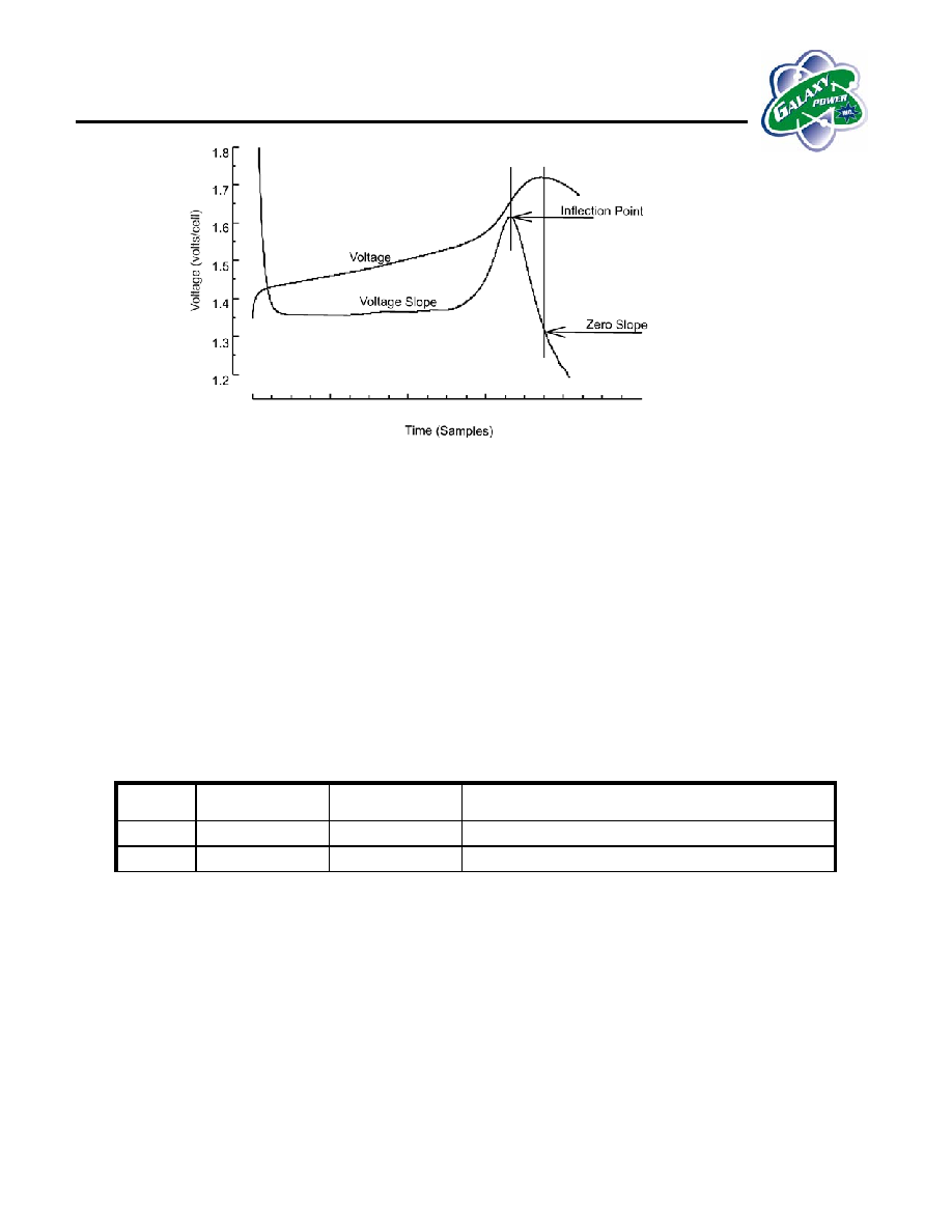
Fig. 6: Voltage and slope curves showing inflection and zero slope points.
The voltage slope is calculated using a modified linear regression algorithm that smoothes the slope. The slope
reachs a maximum, known as the inflection point, prior to the actual voltage peak as shown in Fig. 6. Using
milestone voltage data stored during the charging progress and applying appropriate thresholds, the QSC1702-
MOT 68HRC05 determines full charge and accurately terminates the applied current in between the inflection
point and peak voltage, prior to overcharge.
New, overdischarged, old, and already full batteries produce a voltage profile that varies from that shown in Fig. 6.
The QSC1702-MOT 68HRC05 fast charge termination in these cases is based on a slight decrease in the
voltage. Some new and old batteries may need several charge use cycles before their response stabilizes to that
shown in Fig. 6.
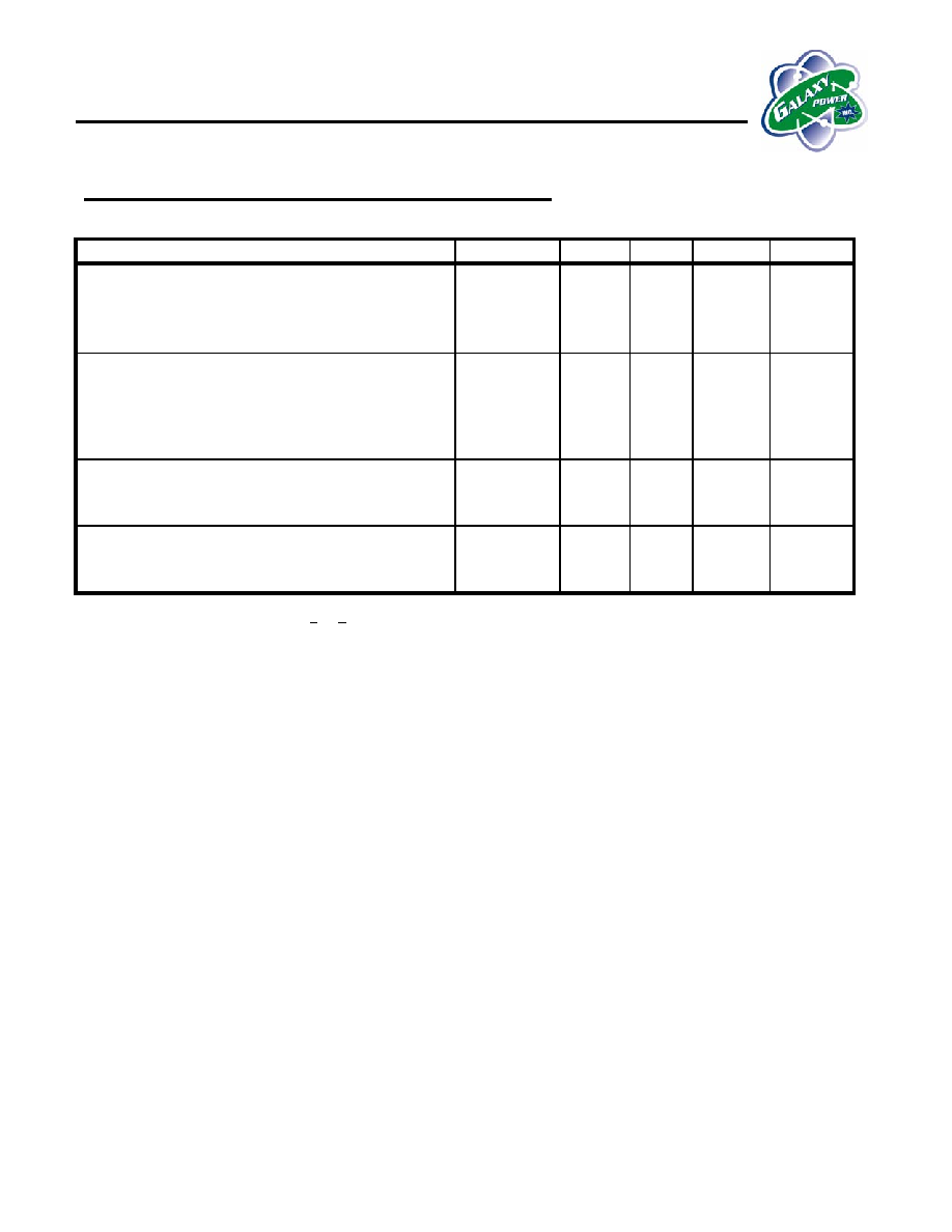
Fast Charge Timer
As a safety back-up the QSC1702-MOT 68HRC05 uses a timer to end fast charge and begin the topping charge.
These times for the standard rates are listed below in Table 1. These times allow the use of charging currents that
aren't exact multiples of the C rate.
Charge
Rate
Fast Charge
Time (nominal)
Fast Charge
Time Limit
Maximum Time Before Initial Slope Check
(after power up)
1 C
60 min.
75 min.
4.3 min.
C/2
120 min.
144 min.
6.5 min.
Table 1: Fast Charge Time Limit and Initial Slope Check Information
Initial Slope Check
The initial slope check is a test to detect a fully charged battery at the beginning of fast charge after soft start.
Once the soft-start sequence completes, voltages are acquired, added together, and averaged to be stored as a
sample. The number of acquisitions to be averaged varies with charge rate. The last column indicates the
elapsed time from powerup that the standard QSC1702-MOT 68HRC05 uses to determine a charge was started
on an already fully charged battery.
If the battery voltage decreases over the sampling period, the battery is assumed to be fully charged. The
QSC1702-MOT 68HRC05 then enters the topping stage. If the battery voltage increases over the sampling
period, the QSC1702-MOT 68HRC05 stores the slope and continues charging.

GPI Internal Information Only
Revision 2.1 - March 19, 2003
QSC1702-MOT 68HC05
Battery Status
Missing battery detection
A continuously available polling mode is provided. A missing battery is determined when: 1) The battery voltage
A/D count is higher than the highest expected count that occurs with a battery present when the charge line
(CHG) is ON, and 2) the battery voltage A/D count is lower than the lowest expected count that occurs with a
battery present when the charge line command (CHG) is OFF. The charge line (CHG) remains ON for
approximately 100ms out of 624ms for polling. After each polling pulse, and a rest, a discharge pulse (equivalent
to one (1) of the six 5ms discharge pulses implemented on powerup) is used until battery is detected. The duty
cycle and time of the polling pulse insures that battery removal or insertion is detected within three seconds. The
standard algorithm produces a 1Hz PFN ON/OFF pattern (.5 second ON/ .5 second OFF) for a suspect battery
(i.e. possible shorted cells) while fast charge progresses. The PFN blink indicator is also used when there is an
open battery with a thermistor present prior to the start of fast charge. This condition occurs when the thermistor
is in normal range, but the battery voltage input indicates an open. If no thermistor is present in the pack, the
indication is PFN ON (no battery for an open battery).
With a normal temperature (5
∞
C to 45
∞
C) battery insertion, fast charge (i.e. soft start) begins. A low battery
voltage count with CHG OFF does not activate the polling mode as long as the battery voltage count does not
exceed 4928 per Figure 7.1 the blinking PFN with CMN.
When in the topping and maintenance charge stages (MMN ON), the QuickSaver
code checks to see if the
battery has been removed. It first looks for the "battery voltage" being much lower than the lowest expected
voltage (count = 1408) that occurs with a battery present when the charge line command (CHG) is OFF. If so
then the charge line command (CHG) is promptly turned ON as a test to see if the battery voltage is much higher
than the highest expected voltage (count = 4928) with a battery. If both conditions occur, the battery has been
removed and the polling mode must initiate. However if the battery voltage during the test to turn ON of CHG is
normal as expected with a battery present but low with CHG OFF, then topping and maintenance continues, even
though the test during the turn OFF of CHG indicates an abnormally low battery voltage (i.e. a count of lower than
1408 in Figure 7.1 battery Voltage A/D Count). One of the "Charge complete-battery with shorted cell" indicates
for this condition in Section 7.0 Algorithm Output Example.
The CHG ON pulse for battery present in topping/maintenance is short in duration (100ms) so it repeats every 3
seconds maximum. A normal 5ms discharge pulse DCHG ON follows the CHG ON pulse before the CHG OFF
battery voltage is checked.
Hot and Cold Battery
A pull-up resistor connected to the NTC thermistor (typically 10K
@ 25∞C) is required to produce a voltage
representative of battery temperature. Thermistor voltage count comparisons are to be used to provide hysteresis
(actual versus established count references in Figure 7.2). The cold battery hysteresis should be 5
∞C. Fast
charging may initiate on a newly installed battery as long as the battery temperature is in the normal range (5
∞C to
45
∞C). If the battery's temperature is less than 5∞C, the topping/maintenance mode commences. In this example,
MMN blinks and OTN is ON. When a newly installed battery warms above 5
∞C, fast charge starts and the fast
charge timer is enabled. Once fast charge starts after a warm-up or upon a normal temperature battery insertion,
fast charge continues as long as the battery temperature stays above 0
∞C. If the battery temperature drops below
0
∞C during fast charge, fast charge terminates. In this example, this is accomplished using the standard voltage
slope algorithm by turning the CHG and DCHG lines OFF; CMN remains ON but fast charge termination occurs
promptly as the battery voltage declines, then MMN goes ON. After fast charge ends due to the battery becoming
cold, OTN remains ON as the topping charge is applied. The cold battery indication is always available to
activate. A warm-up in the topping/maintenance mode after a cold battery end to fast charge only causes OTN to
go OFF. MMN continues to indicate charge complete and the CHG line continues to apply the
topping/maintenance charge after the warm up. DCHG line activates as it normally does.

GPI Internal Information Only
Revision 2.1 - March 19, 2003
QSC1702-MOT HC6805
The hot battery hysteresis should be 15
∞C. Fast charging may initiate on a newly installed battery as long as the
battery temperature is in the normal range (5
∞C to 45∞C). If the battery temperature is above 45∞C, the charge line
(CHG), discharge line (DCHG), and CMN indicator are OFF and in this example OTN blink (1Hz) hot battery
indication activates. When a newly installed hot battery cools to 45
∞C, fast charge starts and the fast charge timer
is enabled. Once fast charge starts after the hot battery cools to 45
∞C, or with a normal temperature battery
insertion, the battery temperature may rise to as high as 60
∞C in fast charge. Fast charge terminates if the battery
temperature rises above 60
∞C. Fast charge termination is to be accomplished using the standard voltage slope
algorithm by turning the CHG and DCHG lines OFF. CMN indicates fast charge even while CHG and DCHG are
OFF due to the battery getting hot. The hot battery OTN blink indication is immediate so it is present with CMN
then CMN goes OFF and MMN goes ON with OTN blinking. Fast charge termination occurs promptly as the
battery voltage declines. After fast charge ends due to the battery becoming hot, MMN indicates charge complete
and the topping charge timer starts, however no topping charge or maintenance charge is actually applied due to
CHG pin being OFF and DCHG is also held OFF until the battery cools to 45
∞C. OTN blinks with MMN ON until
the battery cools below 45
∞C then OTN goes OFF.
A battery that finishes fast charge with its temperature greater than 45
o
C but less than 60
o
C will continue to have
the normal topping charge applied. However a battery that finishes fast charge below 60
o
C, but exceeds 60
o
C
while in topping will cause the CHG and DCHG lines to go OFF while MMN continues to indicate charge
complete. The topping/maintenance timer continues to run but topping/maintenance charge is not applied (CHG
and DCHG remain OFF) until the battery temperature drops below 45
o
C. Then topping/maintenance charge
resumes as CHG and DCHG are allowed to go back ON.
Hot and Cold Battery in Discharge Only Mode
When in the discharge only mode, a discharge will not start on a hot battery (a battery temperature above 45
o
C
per the battery's thermistor voltage count). The MMN and OTN indicators both blink at a 1 Hz rate as per Section
7.0 Algorithm Output Example until the battery temperature cools down below 45
o
C. Once discharge starts, a
battery continues to discharge unless its temperature exceeds 60
o
C, whereupon the DCHG line is turned OFF
while both the MMN and OTN indicators blink at a 1 Hz rate. Discharge begins again (DCHG line ON and OTN
OFF) after the battery cools down below 45
o
C and continues as long as the battery temperature stays below
60
o
C. The process repeats again if the battery exceeds 60
o
C and continues to repeat until the discharge
completes. The discharge complete occurs when the divided down battery voltage drops to 1V (count = 2816).
The MCU shuts down when the discharge algorithm completes in a manner similar to the original ICS1702
algorithm.
A battery that is cold (i.e. less than 5
o
C) does not interfere with the discharge only mode. If the battery is cold, the
MMN and OTN indicators both blink at a 1 Hz rate as per Table 2 Algorithm Output Example. If the battery warms
above 5
o
C during discharge, the OTN indicator goes OFF. If the battery cools below 0
o
C during discharge, the
OTN indicator blinks at a 1Hz rate. The MCU shuts down when the discharge algorithm completes.
A battery pack with an open cell is detected by sensing the presence of the thermistor in conjunction with the
polling mode using sensing techniques previously mentioned. PFN blinks for this condition.
Note: For packs with a different number of cells (10 and 12 cells for example) the packs must be physically
different so that the voltage divider in the charger is changed appropriately. To determine that a battery has
shorted cells requires this input from the battery pack . The charger must be set up by the battery pack at the
time of insertion by a mechanical means (terminal arrangement or in-well switches) so the number of cells is
known. This is the only practical way voltage measurements reveal shorted cells. An overdischarged but
otherwise healthy battery pack may cause a short term shorted cell indication. This occurrence should not
interfere with normal fast charge as the CHG line turns ON with the PFN blink indication continuing.
GPI Internal Information Only
Revision 2.1 - March 19, 2003
QSC1702-MOT 68HC05
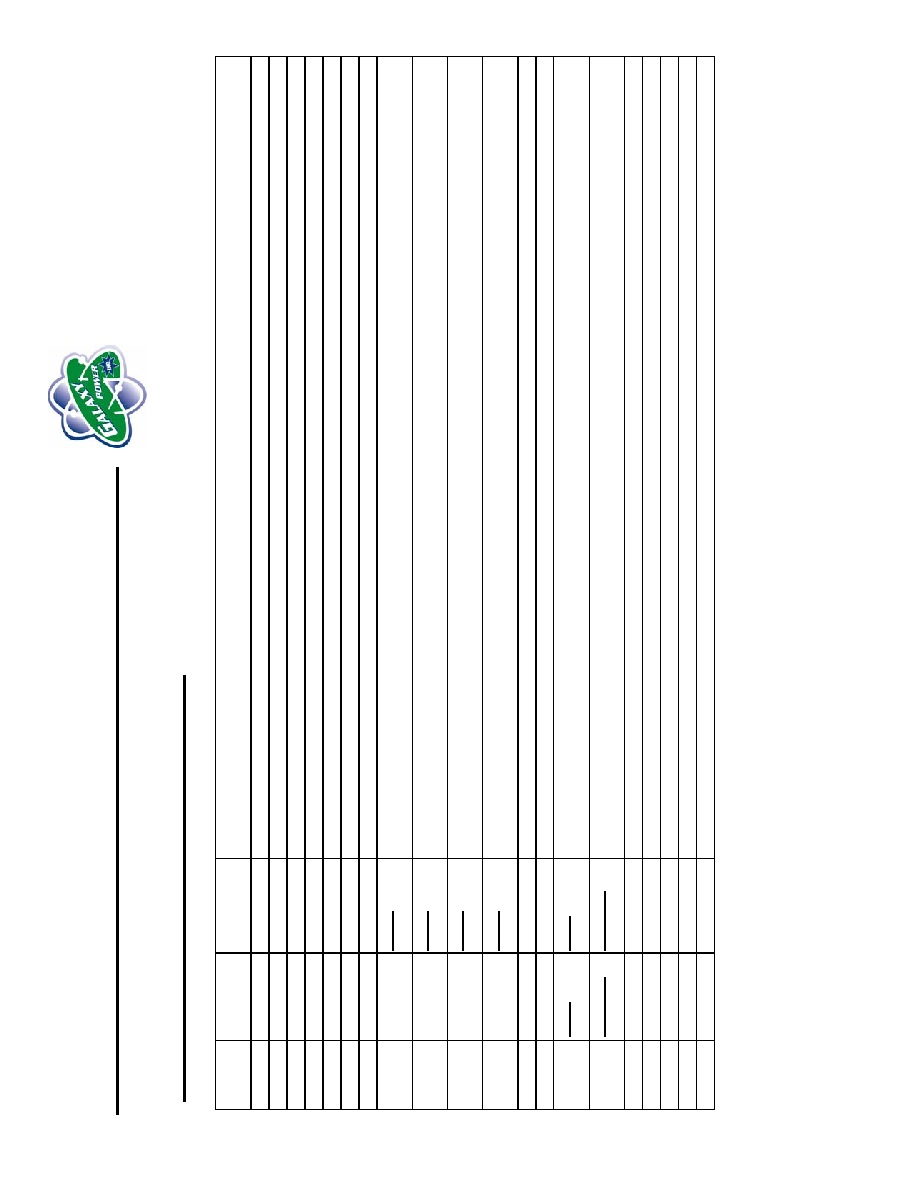
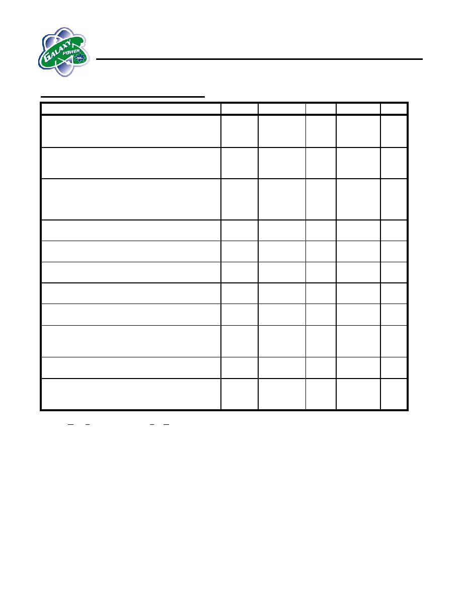
Algorithm Output Example
OTN
MMN
CMN
PFN
CHG and DCHG: DUTY CYCLE (MODE DESCRIPTION)
OFF
OFF
ON
OFF
SOFT START-FAST CHARGE DUTY CYCLE (NORMAL FAST CHARGE)
OFF
ON
OFF OFF
TOPPING/MAINTENANCE DUTY CYCLE (CHARGE COMPLETE)
OFF OFF OFF ON
POLLING DUTY CYCLE (MISSING BATTERY OR OPEN BATTERY WITH NO
THERMISTOR)
ON BLINK OFF OFF
TOPPING/MAINTENANCE DUTY CYCLE(COLD BATTERY INSERTION- WAITING
UNTIL BATTERY WARMS)
BLINK
OFF OFF OFF
CHG AND DCHG DUTY CYCLE OFF (HOT BATTERY INSERTION-WAITING UNTIL
BATTERY COOLS)
OFF OFF ON BLINK
SOFT START/FAST CHARGE CONTINUES NORMALLY (POSSIBLE SHORTED
CELLS)
ON ON OFF OFF
TOP/MAINT DUTY CYCLE (CHARGE COMPLETE-BATTERY COLD)
BLINK ON OFF OFF
CHARGE COMPLETE-BATTERY HOT-DUTY CYCLE OFF
OFF
DATA ON OFF
NORMAL FAST CHARGE (DIAGNOSTIC DATA OUTPUT AUX MODE)
OFF
BLINK
OFF OFF
DCHG (DISCHARGE ONLY AUX MODE)
BLINK BLINK OFF OFF
DCHG (DISCHARGE ONLY AUX MODE) WITH BATTERY COLD OR HOT. MODE
WAITS FOR A HOT BATTERY TO COOL BEFORE STARTING OR
RECOMMENCING. MODE DISCHARGES COLD BATTERY.
OFF OFF OFF BLINK
POLLING DUTY CYCLE (OPEN BATTERY WITH RESIDENT THERMISTOR)
OFF
ON
OFF
BLINK
TOPPING/MAINTENANCE DUTY CYCLE (CHARGE COMPLETE-BATTERY WITH
SHORTED CELLS)
BLINK ON OFF
BLINK
CHG AND DCHG DUTY CYCLE OFF (CHARGE COMPLETE-HOT BATTERY WITH
SHORTED CELLS)
ON ON OFF
BLINK
TOPPING/MAINTENANCE DUTY CYCLE (CHARGE COMPLETE-COLD BATTERY
WITH SHORTED CELLS)

GPI Internal Information Only
Revision 2.1 - March 19, 2003
QSC1702-MOT HC6805
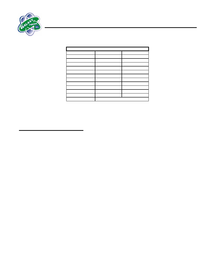
Figure 7.1 -Battery Voltage A/D Count
1V = 1408 (12 bit)
BEFORE STARTING FAST CHARGE
DURING FAST CHARGE
TOPPING/MAINTENACE
VIN COUNT
2.909
1.750
MAX 4096
2014
∑ PFN
ON
∑ NO
BATTERY
∑ (POLL)
∑ PFN
ON
∑ NO
BATTERY
∑ (POLL)
∑ PFN
ON
∑ NO
BATTERY
∑ (POLL)
∑ CHG
ON
∑ CHG
ON
∑ CHG
ON
1.000
1408
2816
3380
0.500
704
∑ CHG
OFF
NO BATTERY
∑ OK
TO
START FAST
CHARGE
∑ CHG
OFF
∑ BATTERY
REMOVED?
∑ SHORTED
CELL (s)
∑ PFN
BLINK
∑ CMN
ON
∑ CHG
ON
∑ CHG OFF
∑ BATTERY
∑ REMOVED?
∑ SHORTED
CELL (s)
∑ PFN
BLINK
∑ MMN
ON
0.000 0
∑
∑
∑
MIN
COUNT
GPI Internal Information Only
Revision 2.1 - March 19, 2003
QSC1702-MOT 68HC05
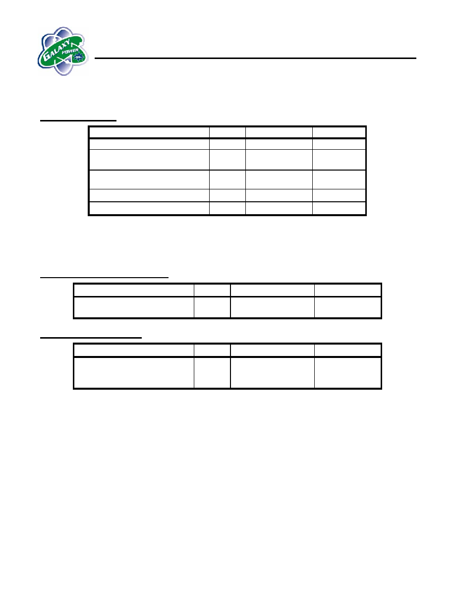
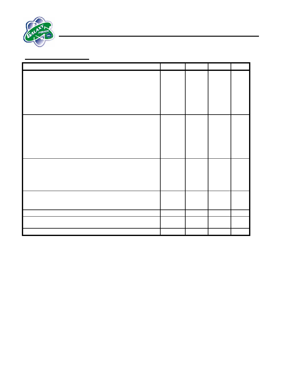
Figure 7.2 - Thermistor Voltage A/D Count
High = Cold, Low = Hot, 1V=1408 (12 bit)
BEFORE STARTING FAST
CHARGE
DURING FAST CHARGE
TOPPING/MAINTENANCE
VTHERM TEMP COUNT
2.9090
MAX 4096
∑ PFN
ON
∑ BATTERY VERY COLD OR NO BATTERY
∑ (POLL
MODE)
∑ OTN
ON
∑ CMN
ON
∑ FAST
CHARGE
∑ CHG& DCHG OFF
∑ OTN
ON
∑ MMN
ON
∑ TOPPING
∑ CHG & DCHG ON
2.3729
0C
3341
∑ OTN
ON
∑ APPLY TOPPING UNTIL
COLD BATTERY WARMS TO
5C
2.1081
5C
2968
∑ OK TO START FAST
CHARGE
0.7044
45C
942
∑ WAIT UNTIL HOT BATT
COOLS TO 45C
∑ OTN
OFF
∑ CMN
ON
∑ FAST
CHARGE
∑ CHG
ON
∑ DCHG
ON
∑ TOPPING
CHARGE
∑ CHG
ON
∑ MMN
ON
∑ OTN
OFF
∑ DCHG
ON
0.4646
60C
654
0.000
0
∑ OTN
BLINK
∑ CHG
OFF
∑ DCHG
OFF
∑ CMN
ON
∑ FAST
CHARGE
∑ CHG
OFF
∑ DCHG
OFF
∑ OTN
BLINK
∑ NO TOPPING CHG
∑ CHG
OFF
∑ DCHG
OFF
∑ MMN
ON
∑ OTN
BLINK
MIN
COUNT
GPI Internal Information Only
Revision 2.1 - March 19, 2003
QSC1702-MOT HC6805
Figure 7.3 - Example of 20 pin 68HC705 Functions
MCU
(pin#)
MCU
name
GPI name
GPI description
1 PB1 VREF REFERENCE
VOLTAGE
2
PB2
VIN
BATTERY VOLTAGE INPUT
3 PB3 THERM
THERMISTOR VOLTAGE INPUT
4
PB4
SEL0
H=1C (1 HR), L=C/2 (2HR), {SPARE IF CHARGE RATE SET BY CODE}
5 PB5 SEL1 {SPARE, CAN BE RESERVED FOR MODIFIED STANDARD AND CUSTOM VERSIONS}}
6
PB6
AUX0
H=NORMAL FAST CHARGE, L=DISCHARGE ONLY, {SPARE IF CHARGE MODE SET BY CODE}
7
PB7
AUX1
H=DATA OUTPUT DISABLED, L=DATA OUTPUT ENABLED, {SPARE IF AUX MODE SET BY CODE}
8
PA5
OTN
ON=COLD BATTERY, BLINK (1 Hz)=HOT BATTERY, {SPARE IF MULTIPLE LED PATTERNS USED}
9
PA4
CMN
CHARGE INDICATOR, ON=SOFTSTART/FAST CHARGE
10
PA3
MMN
ON=CHARGE COMPLETE, FLASH WITH CMN ON =DATA OUTPUT, BLINK WITH OTN ON=COLD BATTERY
UPON INSERTION, BLINK DISCHARGE ONLY
11
PA2
PFN
ON=MISSING BATTERY, BLINK (1 Hz=SHORTED CELLS, OPEN PACK WITH THERMISTOR), {SPARE IF
MULTIPLE LED PATTERNS USED}
12 PA1 DCHG DISCHARGE
ON/OFF
13
PA0
CHG
CURRENT SOURCE ON/OFF
14
IRQ/Vpp
IRQ/Vpp
INTERUPT REQUEST/ONE TIME PROGRAMMING PIN
15
RESET
RESET
RESET
16 OSC2 RC2 CLOCK
2
17 OSC1 RC1 CLOCK
1
18 VSS VSS GROUND
19 VDD VDD +5V
POWER
20
PB0
CAP
CAP FOR ADC

GPI Internal Information Only
Re vision 2.1 - March 19, 2003
QSC1702-MOT HC6805
Set-up Information
The QSC1702-MOT 68HRC05 requires some external components for 5V power to VDD. A resistor to set the
clock, dividers to sense battery voltage and set the 1V reference, and a pull-up resistor to 5V to sense
temperature. Also, interfaces to an external current source and to a transistor and resistor for discharge pulse
conditioning and discharge AUX mode. The QSC1702-MOT 68HRC05 does not control the amplitude of current
flowing into the battery in any way other than switching it ON and OFF. The current for the selected charge rate is
provided by a regulated current source. The constant current source is set according to the charge rate selected.
For example, to charge a 1.2 ampere hour battery at the 120 minute (1/2C) rate, a 0.6 amp current is needed.
Charge
Rate
Fast Charge
Time (nominal)
Topping Charge
Pulse Period
Maintenance Charge
Pulse Period
Fast Charge
Timer
1 C
60 min. (1 hr)
14 sec
54 sec
75 min.
1/2 C
120 min. (2 hr)
8 sec
28 sec
144 min.
Table 3: Charge Rate Information (Ref. Fig. 5)
Applications Information
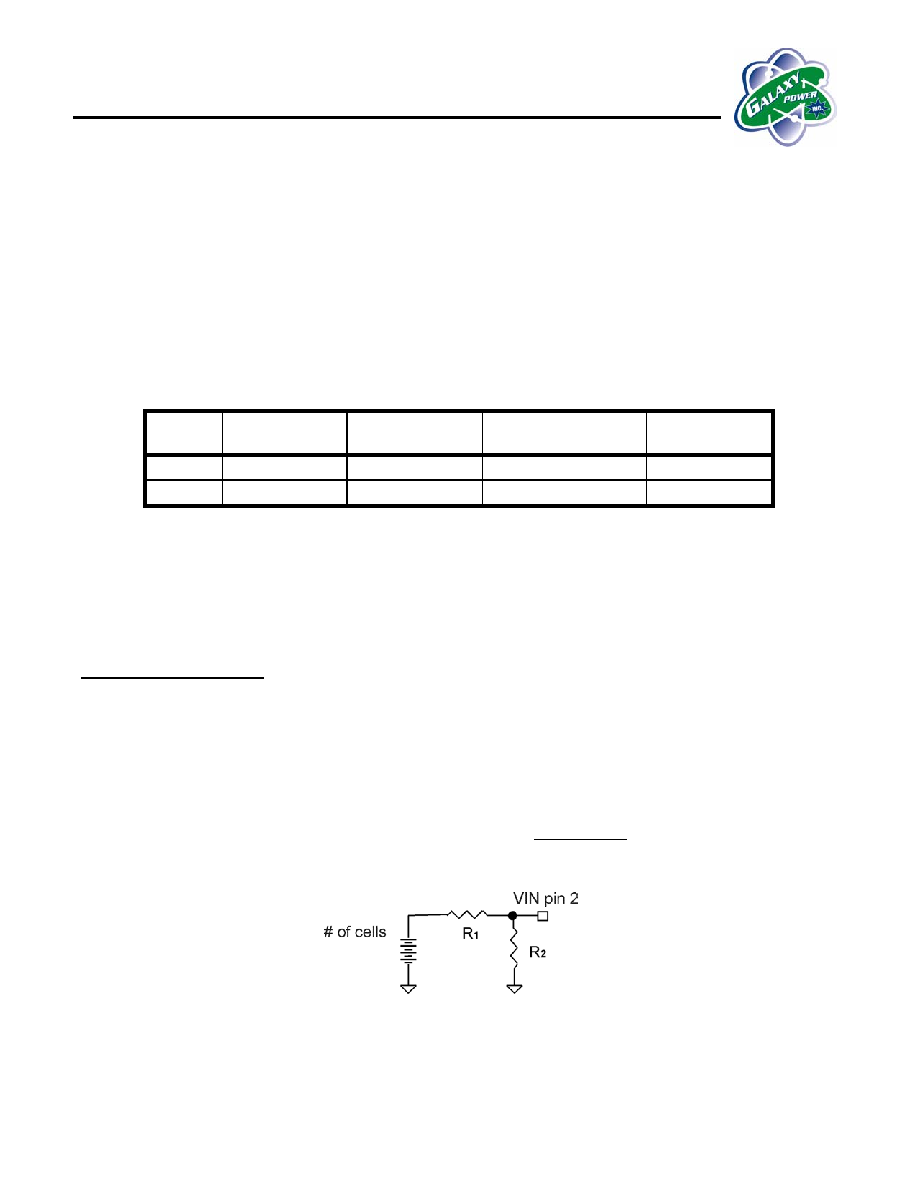
VIN Divider Resistors
R1 and R2 must be selected properly to ensure that battery detection and voltage termination methods operate
properly. Refer to Figure 8. R1 and R2 are selected to scale the battery voltage down to the voltage of one cell
for NiCd and NiMH batteries. A normalized battery voltage is applied to the voltage sense (VIN) pin. The battery
voltage is normalized using a resistor divider providing the voltage representative of one cell. For example, if the
battery consists of six cells in a series, the voltage at the VIN pin must be equal to the total battery voltage divided
by six. This is accomplished with two external resistors. To determine the correct resistor values, count the
number of cells to be charged in series. Then choose either R
1
or R
2
and solve for the other resistor using:
(
)
(
)
R
R
R
R
1
2
2
1
1
1
=
◊
-
=
-
#
#
of cells
or
of cells
Fig. 8: Resistor divider network at the VIN pin 2.
GPI Internal Information Only
Revision 2.1 - March 19, 2003
QSC1702-MOT 68HC05
The following table shows some typical values for NiCd and NiMH batteries:
Cells R1
R2
1 20K
*
2 20K
20K*
3 39K
20K
4 62K
20K
5 82K
20K
6 100K
20K
7 120K
20K
8 150K
20K
9 160K
20K
10 180K
20K
11 200K
20K
12 220K
20K
13 & Above
R1=R2 x (# cells - 1)
* Use 5.1V Zener as required depending on input voltage
To ensure proper operation of the QSC1702-MOT 68HRC05, external components must be properly selected.
The external current source used must meet several important criteria to ensure adequate performance of the
charging system. The charging current source amplitude should be fairly constant.
Temperature Sense: THERM Pin
The THERM input uses a 15.8K external pull-up resistor for battery temperature sensing along with a 10K
at 25∞
C NTC thermistor such as the Semitec USA (Ishizuka Electronics Corp.) part # AT103-1 (2).

GPI Internal Information Only
Re vision 2.1 - March 19, 2003
QSC1702-MOT HC6805
Using the Voltage Slope Termination Method
If the current source is a switch mode type, normal switch mode ripple current does not effect the QSC1702-MOT
68HRC05. However, the effects of line frequency ripple may interfere with proper performance.
In general the voltage slope termination method works best for products where the battery is fast charged with the
product off, or the battery is removed from the product for fast charge in a charger stand.
The voltage slope termination method used by the QSC1702-MOT 68HRC05 requires a fairly constant amplitude
current flow into the battery during fast charge. Charging the battery in products that draw a known and fairly
constant current while the battery is charging should have this current draw added to the fast charge current.
Using the QSC1702-MOT 68HRC05 for charging the batteries in products that randomly or periodically requires
moderate current from the battery during fast charge needs evaluation. Products that randomly or periodically
require high current from the battery during fast charge may cause a voltage inflection that results in termination
before full charge. A voltage inflection can occur due to the charge current decreasing or fluctuating as the load
changes rather than by the battery reaching full charge. The voltage slope method can terminate charge based
on voltage inflections that resemble that of a fully charged battery. The QSC1702-MOT 68HRC705 can be
supplied as a temperature slope only modified standard version.
Charging sources that produce decreasing current as fast charge progresses may also cause a voltage inflection
that may result in termination before full charge. For example, if the charge current is supplied through a resistor
or if the charging source is a constant current type that has insufficient input voltage, the current will decrease and
may cause a termination before full charge. Other current source abnormalities that may cause a voltage
inflection that is characteristic of a fully charged battery are inadequate line frequency ripple attenuation cr charge
current decreasing due to thermal drift or thermal limiting. Charging sources that have any of the above
characteristics need evaluation to access their suitability for the application if the use of voltage slope termination
is desired.
The controller SoftStart stage, built-in noise filtering, and fast charge timer operate optimally when the constant
amplitude current source charges the battery at the rate selected. If the actual charge current is significantly less
than the rate selected, the conditioning effect of the SoftStart stage and the controller noise immunity are
lessened. Also, the fast charge timer may cause termination based on time duration rather than by the battery
reaching full charge due to inadequate charge current.
PC Board Design Considerations
It is very important that care be taken to minimize noise coupling and ground bounce. Careful placement of wires
and connectors helps minimize resistance and inductance.
When designing the printed circuit board, make sure ground and power traces are wide and bypass capacitors
are used right at IC power and ground pins. Use separate heavy grounds for both signal and power circuits,
connecting their grounds together close to where the negative lead of the battery connects. For power circuits,
keep the physical separation between power and return (ground) to a minimum to minimize field effects. This
precaution is most applicable to the constant current source, particularly if it is a switch mode type. Keep the
QSC1702-MOT 68HRC05 and the constant current source control circuits outside the power and return loop
described above. These precautions will prevent high fields and coupled noise from disturbing normal operation.
Avoid jumping across power and return with signal lines.
GPI Internal Information Only
Revision 2.1 - March 19, 2003
QSC1702-MOT 68HC05
Data Tables
Maximum Ratings
Parameter Symbol
Value
Units
Supply Voltage
V
DD
-0.3 to + 7.0
V
Bootloader/Self-Check Mode
(IRQ/Vpp Pin Only)
V
IN
Vss -0.3 to 17
V
Current Drain Per Pin Excluding
V
DD
and V
SS
I 25
mA
Operating Junction Temperature
T
J
+150 ∞C
Storage Temperature Range
T
stg
-65 to +150
∞C
Stresses above those listed under Absolute Maximum Ratings may cause permanent damage to the device. This
is a stress rating only and functional operation of the device at these or other conditions above those listed in this
document is not intended. Exposure to absolute maximum ratings adversely affects product performance.
Operating Temperature Range
Characteristic Symbol
Value
Unit
Operating Temperature Range
Extended
T
A
T
L
to T
H
-40 to +85
∞C
Thermal Characteristics
Characteristic Symbol
Value
Unit
Thermal Resistance
Plastic
SOIC
JA
60
∞C/W
GPI Internal Information Only
Re vision 2.1 - March 19, 2003
QSC1702-MOT HC6805
Supply Current Characteristics (V
DD
= 4.5 to 5.5 Vdc)
Characteristic Symbol
Min
Typ
Max
Unit
RUN (Analog and LVR Disabled)
Internal Low-Power Oscillator at 100 kHz
Internal Low-Power Oscillator at 500 kHz
Extrernal Oscillator Running at 4.2 MHz
I
DD
-
-
-
150
375
3.00
568
1100
5.20
µA
µA
µA
WAIT (analog and LVR Disabled)
Internal Low-Power Oscillator at 100kHz
Internal Low-Power Oscillator at 500 kHz
Extrernal Oscillator Running at 4.2 MHz
I
DD
-
-
-
45
75
1.00
85
375
2.20
µA
µA
µA
STOP (Analog and LVR Disabled)
25
∞C
-40
∞C to 85∞C
I
DD
-
-
2
4
10
20
µA
µA
Incremental I
DD
for Enabled Modules
LVR
Analog Subsystem
I
DD
-
-
5
380
15
475
µA
µA
NOTES:
1. V
DD
= 4.5 to 5.5 Vdc, V
SS
= 0 V, T
L
< T
A
< T
H
, unless otherwise noted.
2.
All values shown reflect average measurements.
3.
Typical values at midpoint of voltage range, 25
∞C only.
4. Run
(Operating)
I
DD
, Wait I
DD
: Measured using external square wave clock source to OSC1 pin or internal oscillator, all inputs 0.2 Vdc
from either supply rail (V
DD
or V
SS
); no dc loads, less than 50 pF on all outputs, C
L
= 20 pF on OSC2.
5. Wait
I
DD
is affected linearly by the OSC2 capacitance.
6. Stop
I
DD
: All ports configured as inputs, V
IL
= 0.2 Vdc, V
IH
= V
DD
- 0.2Vdc, OSC1 = V
DD
.
GPI Internal Information Only
Revision 2.1 - March 19, 2003
QSC1702-MOT 68HC05
DC Electrical Characteristics (5.0 Vdc)
Characteristic Symbol
Min
Typ
Max
Unit
Output Voltage
I
LOAD
= 10.0
µA
I
LOAD
= -10.0
µA
V
OL
V
OH
-
V
DD
- 0.1
-
-
0.1
-
V
Output High Voltage
(I
LOAD
= -0.8
mA) PB0:7
(I
LOAD
= -4.0
mA) PA0:5, PB4
V
OH
V
DD
- 0.8
V
DD
- 0.8
-
-
-
-
V
Output Low Voltage
(I
LOAD
= 1.6 mA) PB0:7, RESET
(I
LOAD
= 10 mA) PA0:5, PB4
(I
LOAD
= 15
mA) PA0:5, PB4
V
OL
-
-
-
-
-
-
0.4
0.4
1.5
V
High Source Current
Total for All (6) PA0:5 Pins and PB4
I
OH
-
-
20
mA
High Sink Current
Total for All (6) PA0:5 Pins and PB4
I
OL
-
-
40
mA
Input High Voltage
PA0:5, PB0:7, RESET, OSC1, IRQ/V
PP
V
IH
0.7 x V
DD
-
V
DD
V
Input Low Voltage
PA0:5, PB0:7, RESET, OSC1, IRQ/V
PP
V
IL
V
SS
-
0.3 x V
DD
V
Input Current
OSC1, IRQ/V
PP
I
IN
-1
-
1
µA
Input Current
RESET (Pullup, Source)
RESET (Pulldown, Sink)
I
IN
10
-6
-
-
-
-
µA
mA
I/O Ports High-Z Leakage Current (Pulldowns Off)
PA0:6, PB0:7
I
OZ
-2
-
2
µA
Input Pulldown Current
PA0:5, PB0:7 (V
IN
= V
IH
= 0.7 x V
DD
)
PA0:5, PB0:7 (V
IN
= V
IL
= 0.3 x V
DD
)
I
IL
40
25
100
65
280
190
µA
NOTES:
1. +4.5
<
V
DD
< +5.5 V, V
SS
= 0 V, T
L
< T
A
< T
H
, unless otherwise noted.
2.
All values shown reflect average measurements.
3.
Typical values at midpoint of voltage range, 25
∞C.
GPI Internal Information Only
Re vision 2.1 - March 19, 2003
QSC1702-MOT HC6805
Analog Subsystem Characteristics (5.0 Vdc)
Characteristic Symbol
Min
Max
Unit
Voltage Comparators
Input Offset Voltage
Common-Mode Range
Comparator 1 Input Impedance
Comparator 2 Input Impedance
Direct Input to Comparator 2 (HOLD=1, DHOLD=0)
Divider input to Comparator 2 (HOLD=0, DHOLD=1)
V
IO
V
CMR
Z
IN
Z
IN
Z
IN
-
-
800
800
80
15
V
DD
-1.5
-
-
-
mV
V
k
k
k
Input Divider Ratio (Comparator 2, HOLD=0, DHOLD=1)
V
IN
= 0 to V
DD
-1.5V
R
DIV
0.49
0.51
Analog Subsystem internal V
SS
Offset
Sum of comparator offset and IR drop through V
SS
V
AOFF
20
40
mV
Channel Selection Multiplexer Switch Resistance
R
MUX
-
3 k
External current Source (PB0/AN0)
Source Current (V
OUT
= V
DD
/2)
Source Current Linearity (V
OUT
= 0 to V
DD
-1.5 Vdc)
Discharge Sink Current (V
OUT
= 0.4V)
I
CHG
I
CHG
I
DIS
85
-
1.1
113
+ 1
-
µA
%FS
mA
External Capacitor (connected to PB0/AN0)
Voltage Range
Discharge Time
Value of External Ramping Capacitor
V
CAP
t
DIS
C
EXT
V
SS
5
-
V
DD
- 1.5
10
2
V
ms/
µF
µF
Internal Sample and Hold Capacitor
Capacitance
Charge/Discharge Time (0 to 3.5 Vdc)
Direct connection (HOLD=1, DHOLD=0)
Divided Connection (HOLD=0, DHOLD=1)
Temperature Diode Connection (Hold=1, DHOLD=1)
Leakage Discharge Rate
C
SH
t
SHCHG
t
SHDCHG
t
SHTCHG
C
SHDIS
8
1
2
1
-
13
-
-
-
0.2
pF
µs
µs
µs
V/sec
Internal Temperature Sensing Diode
Voltage (at Tj = 25
∞C)
Temperature Change in Voltage
Vd
TCd
0.65
2.0
0.71
2.2
V
mV/
∞C
NOTES:
1. +4.5
<
V
DD
< +5.5 V, V
SS
= 0 V, T
L
< T
A
< T
H
, unless otherwise noted.
GPI Internal Information Only
Revision 2.1 - March 19, 2003
QSC1702-MOT 68HC05
Control Timing (5.0 Vdc)
Characteristic Symbol
Min
Max
Unit
Frequency of Oscillation (OSC)
RC Oscillator Option
Crystal Oscillator Option
External Clock Source
Internal Low-Power Oscillator
Standard Product (100 kHz nominal)
Mask Option (500 kHz nominal, see Note 3)
f
OSC
-
0.1
DC
60
300
4.2
4.2
4.2
140
700
MHz
MHz
MHz
KHz
KHz
Internal Operating Frequency, Crystal, or External Clock (fosc/2)
RC Oscillator Option
Crystal Oscillator Option
External Clock Source
Internal Low-Power Oscillator
Standard Product (100 kHz nominal)
Mask Option (500 kHz nominal, see Note 3)
f
OP
-
0.5
DC
30
150
2.1
2.1
2.1
75
350
MHz
MHz
MHz
KHz
KHz
Cycle time (1/fop)
External Oscillator or Clock Source
Internal Low-Power Oscillator
Standard Product (100 kHz nominal)
Mask Option (500 kHz nominal, see Note 3)
t
CYC
476
14.29
2.86
-
33.33
6.67
ns
µs
µs
16-bit Timer
Resolution
Input Capture (TCAP) Pulse Width
tresl
t
TH
, t
TL
4.0
284
-
-
t
CYC
ns
Interrupt Pulse Width Low (Edge-Triggered)
t
ILIH
284 - ns
Interrupt Pulse Period
t
ILIL
See
Note 2
- t
CYC
OSC1 Pulse Width (External Clock Input)
t
OH
, t
OL
110
-
ns
Note1: For SOIC package, R=110K, 1%. For DIP package, R=105K, 1%.
GPI Internal Information Only
Re vision 2.1 - March 19, 2003
QSC1702-MOT HC6805
Package Information
Ordering Information
M-QSC1702-XX-###
Example:
M-QSC1702-XX-###
Code
version:
XX-###
=
Customer and code version
Prefix:
QSC
=
Q
uick
S
aver
C
ode (1702 core)
MCU manufacturer:
M
= Motorola

GPI Internal Information Only
Revision 2.1 - March 19, 2003
QSC1702-MOT 68HC05
IMPORTANT NOTICE
Galaxy Power Incorporated makes no claim about the capability of any particular battery (NiCd, NiMH, or Li-Ion)
to accept a fast charge. GPI strongly recommends that the battery manufacturer be consulted before fast
charging. GPI shall be held harmless for any misapplication of this device such as: exceeding the rated
specifications of the battery manufacturer; charging batteries other than nickel-cadmium or nickel-metal hydride
type; personal or product damage caused by the charging device, circuit, or system itself; unsafe use, application,
and/or manufacture of a charging system using this device.
GPI reserves the right to make changes in the device data identified in this publication without further notice. GPI
advises its customers to obtain the latest version of all device data to verify that any information being relied upon
by the customer is current and accurate.
GPI does not assume any liability arising out of or associated with the application or use of any product or
integrated circuit or component described herein. GPI does not convey any license under its patent rights or the
patent rights of others described herein. In the absence of a written or prior stated agreement to the contrary, the
terms and conditions stated on the back of the GPI order acknowledgment obtain.
GPI makes no warranty of any kind with regard to this material, including, but not limited to, the implied warranties
of merchantability and fitness for a particular purpose.
GPI products are not designed, intended, or authorized for use as components in systems intended for surgical
implant into the body, or other applications intended to support or sustain life, or for any nuclear facility
application, or for any other application in which the failure of the GPI product(s) could create a situation where
personal injury or death may occur. GPI will not knowingly sell its products for use in such applications, and the
buyer shall indemnify and hold harmless GPI and its officers, employees, subsidiaries, affiliates, representatives
and distributors against all claims, costs, damages, expenses, tort and attorney fees arising out of directly or
indirectly, any claim of personal injury or death associated with such unintended or unauthorized use, even if such
claim alleges that GPI was negligent regarding the design or manufacture of the part.
COPYRIGHT © 2002 Galaxy Power Incorporated

GPI Internal Information Only
Re vision 2.1 - March 19, 2003
QSC1702-MOT HC6805
Galaxy Power, Inc.
2500 Eisenhower Avenue
PO Box 890
Valley Forge, PA 19482-0890
Phone: 610-676-0188
FAX: 610-676-0189
WWW: galaxypower.com
e-mail:
rogers@galaxypower.com
NOTES