Revision 1, May 2002 www.gammamicro.com
1.5A DC-to-DC CONVERTER CONTROL CIRCUIT
GM34063
PRELIMINARY
1
3.0V to 40V input
Adjustable Output Voltage
Current Limiting
Output Switch Current to 1.5A
Low Standby Current
Operating Frequency to 100kHz
Precision 2% Reference
The GM34063 has all the functions required for
DC-to-DC converters: an internal temperature-
compensated reference, comparator, controlled
duty cycle oscillator with an active current limit
circuit, driver, and high-current output switch.
The 34063 designed for step-down, step-up and
voltage-inverting applications using a minimum
number of external components.
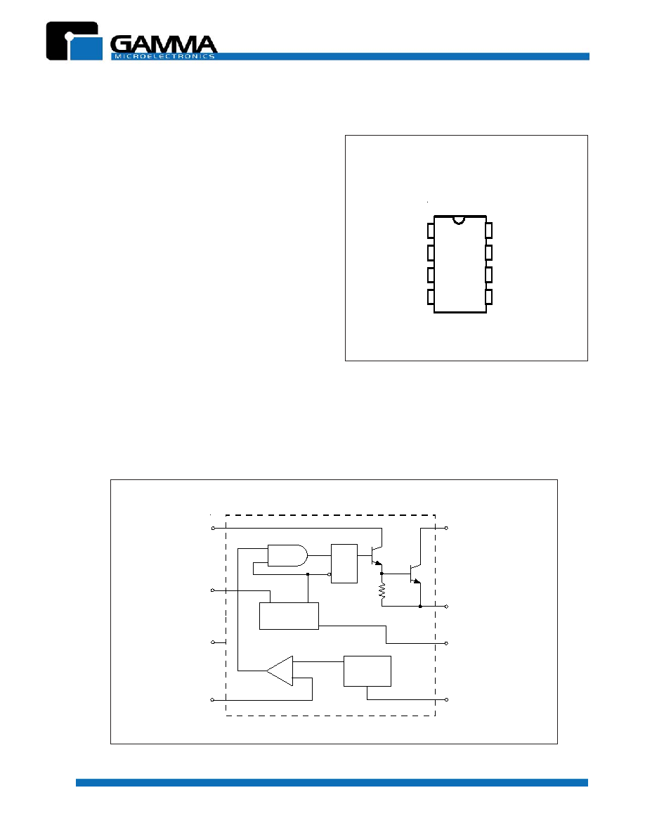
SCHEMATIC DIAGRAM
PIN CONNECTIONS
CD-ROM
Motherboards
SMPS Power Supply
Battery Chargers
Applications:
1
2
3
4
8
7
6
5
Switch
Collector
Driver
Collector
Switch Emitter
Timing
Capacitor
GND
I
pk
Sense
V
CC
Comparator
Inverting unit
(Top View)
8
7
6
5
4
3
2
1
Driver Collector
I
pk
Sense
V
CC
Comparator
Inverting unit
GND
Timing Capacitor
Switch Emitter
Switch Collector
(Bottom View)
S
R
Q
Q2
Q1
100
Comparator
+
-
1.25V
Reference
Regulator
I
pk
Oscillator
C
T
* The GM34063 has 51 active transistors on-chip.
Revision 1, May 2002 www.gammamicro.com
1.5A DC-to-DC CONVERTER CONTROL CIRCUIT
GM34063
PRELIMINARY
Absolute Maximum Ratings
2
g
n
i
t
a
R
l
o
b
m
y
S
e
u
l
a
V
t
i
n
U
e
g
a
tl
o
V
y
l
p
p
u
S
r
e
w
o
P
V
C
C
0
4
c
d
V
e
g
n
a
R
e
g
a
tl
o
V
t
u
p
n
I
r
o
t
a
r
a
p
m
o
C
V
R
I
0
4
+
o
t
3
.
0
�
c
d
V
e
g
a
tl
o
V
r
o
t
c
e
ll
o
C
h
c
ti
w
S
C
V
)
h
c
ti
w
s
(
0
4
c
d
V
V
(
e
g
a
tl
o
V
r
e
tt
i
m
E
h
c
ti
w
S
1
n
i
P
)
V
0
4
=
E
V
)
h
c
ti
w
s
(
0
4
c
V
e
g
a
tl
o
V
r
e
tt
i
m
E
o
t
r
o
t
c
e
ll
o
C
h
c
ti
w
S
E
C
V
)
h
c
ti
w
s
(
0
4
c
d
V
e
g
a
tl
o
V
r
o
t
c
e
ll
o
C
r
e
v
ir
D
C
V
)
r
e
v
ir
d
(
0
4
c
d
V
)
1
e
t
o
N
(
t
n
e
r
r
u
C
r
o
t
c
e
ll
o
C
r
e
v
ir
D
C
I
)
r
e
v
ir
d
(
0
0
1
A
m
t
n
e
r
r
u
C
h
c
ti
w
S
I
W
S
5
.
1
A
s
c
it
s
ir
e
t
c
a
r
a
h
C
l
a
m
r
e
h
T
d
n
a
n
o
it
a
p
i
s
s
i
D
r
e
w
o
P
x
if
f
u
S
1
P
,
P
,
e
g
a
k
c
a
P
c
it
s
a
l
P
T
A
C
�
5
2
=
e
c
n
a
t
s
i
s
e
R
l
a
m
r
e
h
T
x
if
f
u
S
D
,
e
g
a
k
c
a
P
C
I
O
S
T
A
C
�
5
2
=
e
c
n
a
t
s
i
s
e
R
l
a
m
r
e
h
T
P
D
R
2
A
J
P
D
R
2
A
J
5
2
.
1
0
0
1
5
2
6
0
6
1
W
W
/
C
�
W
m
W
/
C
�
e
r
u
t
a
r
e
p
m
e
T
n
o
it
c
n
u
J
g
n
it
a
r
e
p
O
T
J
0
5
1
+
C
�
e
g
n
a
R
e
r
u
t
a
r
e
p
m
e
T
t
n
e
i
b
m
A
g
n
it
a
r
e
p
O
T
A
0
7
+
o
t
0
C
�
e
g
n
a
R
e
r
u
t
a
r
e
p
m
e
T
e
g
a
r
o
t
S
T
g
t
s
0
5
1
+
o
t
5
6
�
C
�
Note 1. Maximum package power dissipation limits must be observed.
Revision 1, May 2002 www.gammamicro.com
1.5A DC-to-DC CONVERTER CONTROL CIRCUIT
GM34063
PRELIMINARY
3
ELECTRICAL CHARACTERISTICS
(V
CC
= 5.0 V, T
A
= T
low
to T
high
unless otherwise specified)
s
c
i
t
s
i
r
e
t
c
a
r
a
h
C
l
o
b
m
y
S
n
i
M
p
y
T
x
a
M
ti
n
U
R
O
T
A
L
L
I
C
S
O
V
(
y
c
n
e
u
q
e
r
F
5
n
i
P
C
,
V
0
=
T
T
,
F
n
0
.
1
=
A
)
C
�
5
2
=
f
c
s
o
4
2
3
3
2
4
z
H
k
V
(
t
n
e
r
r
u
C
e
g
r
a
h
C
C
C
T
,
V
0
4
o
t
V
0
.
5
=
A
)
C
�
5
2
=
I
g
h
c
4
2
5
3
2
4
:
:
:
:
:A
V
(
t
n
e
r
r
u
C
e
g
r
a
h
c
s
i
D
C
C
T
,
V
0
4
o
t
V
0
.
5
=
A
)
C
�
5
2
=
I
g
h
c
s
i
d
0
4
1
0
2
2
0
6
2
:
:
:
:
:A
V
o
t
7
n
i
P
(
o
it
a
R
t
n
e
r
r
u
C
e
g
r
a
h
C
o
t
e
g
r
a
h
c
s
i
D
,
C
C
T
A
)
C
�
5
2
=
I
g
h
c
s
i
d
I/
g
h
c
2
.
5
5
.
6
5
.
7
�
I
(
e
g
a
tl
o
V
e
s
n
e
S
ti
m
i
L
t
n
e
r
r
u
C
g
h
c
I
=
g
h
c
s
i
d
T
,
A
)
C
�
5
2
=
V
)
e
s
n
e
s
(
k
p
i
0
5
2
0
0
3
0
5
3
V
m
)
2
e
t
o
N
(
H
C
T
I
W
S
T
U
P
T
U
O
n
o
it
c
e
n
n
o
C
n
o
t
g
n
il
r
a
D
,
e
g
a
tl
o
V
n
o
it
a
r
u
t
a
S
I
(
W
S
)
d
e
t
c
e
n
n
o
c
8
,
1
s
n
i
P
,
A
0
.
1
=
V
)t
a
s
(
E
C
�
0
.
1
3
.
1
V
)
3
e
t
o
N
(
e
g
a
tl
o
V
n
o
it
a
r
u
t
a
S
I
(
W
S
R
,
A
0
.
1
=
8
n
i
P
2
8
=
S
V
o
t
C
C
d
e
c
r
o
F
,
$ . )
0
2
V
)t
a
s
(
E
C
�
5
4
.
0
7
.
0
V
I
(
n
i
a
G
t
n
e
r
r
u
C
C
D
W
S
V
,
A
0
.
1
=
E
C
T
,
V
0
.
5
=
A
)
C
�
5
2
=
h
E
F
0
5
5
7
�
�
V
(
t
n
e
r
r
u
C
e
t
a
t
S
�
ff
O
r
o
t
c
e
ll
o
C
E
C
)
V
0
4
=
I
)f
f
o
(
C
�
1
0
.
0
0
0
1
:
:
:
:
:A
R
O
T
A
R
A
P
M
O
C
e
g
a
tl
o
V
d
l
o
h
s
e
r
h
T
T
A
C
�
5
2
=
T
A
T
=
w
o
l
T
o
t
h
g
i
h
V
h
t
5
2
2
.
1
0
1
2
.
1
5
2
.
1
-
5
7
2
.
1
9
2
.
1
V
V
(
n
o
it
a
l
u
g
e
R
e
n
i
L
e
g
a
tl
o
V
d
l
o
h
s
e
r
h
T
C
C
)
V
0
4
o
t
V
0
.
3
=
g
e
R
e
n
il
-
4
.
1
0
.
5
V
m
V
(
t
n
e
r
r
u
C
s
a
i
B
t
u
p
n
I
n
i
)
V
0
=
I
B
I
-
0
2
-
0
0
4
-
A
n
E
C
I
V
E
D
L
A
T
O
T
V
(
t
n
e
r
r
u
C
y
l
p
p
u
S
C
C
C
,
V
0
4
o
t
V
0
.
5
=
T
V
=
7
n
i
P
,
F
n
0
.
1
=
C
C
,
V
5
n
i
P
V
>
h
t
)
n
e
p
o
s
n
i
p
g
n
i
n
i
a
m
e
r
,
d
n
G
=
2
n
i
P
,
I
C
C
-
-
0
.
4
A
m
Note 2. Low duty cycle pulse techniques are used during test to maintain junction temperature as close to ambient as possible.
Note 3. If the output switch is driven into hard saturation (non�Darlington configuration) at low switch currents (
#
300 mA) and high driver
currents (
$
30 mA), it may take up to 2.0
�
s for it to come out of saturation. This condition will shorten the off time at frequencies
$
30 kHz,
and is magnified at high temperatures. This condition does not occur with a Darlington configuration, since the output switch cannot
saturate. If a non�Darlington configuration is used, the following output drive condition is recommended:
Forced
of output switch :
I
C
output
$
10
I
C
driver � 7.0 mA *
* The 100
resistor in the emitter of the driver device requires about 7.0 mA before the output switch conducts.

Revision 1, May 2002 www.gammamicro.com
1.5A DC-to-DC CONVERTER CONTROL CIRCUIT
GM34063
PRELIMINARY
4
t
s
e
T
s
n
o
i
t
i
d
n
o
C
s
t
l
u
s
e
R
n
o
it
a
l
u
g
e
R
e
n
i
L
V
n
i
I
,
V
6
1
o
t
V
0
.
8
=
O
A
m
5
7
1
=
%
5
0
.
0
�
=
V
m
0
3
n
o
it
a
l
u
g
e
R
d
a
o
L
V
n
i
I
,
V
2
1
=
O
A
m
5
7
1
o
t
A
m
5
7
=
%
7
1
0
.
0
�
=
V
m
0
1
e
l
p
p
i
R
t
u
p
t
u
O
V
n
i
I
,
V
2
1
=
O
A
m
5
7
1
=
p
p
V
m
0
0
4
y
c
n
e
i
c
if
f
E
V
n
i
I
,
V
2
1
=
O
A
m
5
7
1
=
%
7
.
7
8
r
e
tl
i
F
l
a
n
o
it
p
O
h
t
i
W
e
l
p
p
i
R
t
u
p
t
u
O
V
n
i
I
,
V
2
1
=
O
A
m
5
7
1
=
p
p
V
m
0
4
Step�Up Converter
170
�
H
180
6
5
4
7
8
+
3
2
1
100
V
in
12 V
R
sc
0.22
+
+
1N5819
1500 pF
330
100
V
out
1.0
�
H
47k
R2
2.2k
R1
C
O
V
out
28 V / 175 mA
L
S
R
Q
Q2
Q1
+
1.25V
Reference
Regulator
I
pk
Osc.
C
T
-
V
CC
Optional
Filter
Comp.
C
T
Revision 1, May 2002 www.gammamicro.com
1.5A DC-to-DC CONVERTER CONTROL CIRCUIT
GM34063
PRELIMINARY
5
External NPN Switch
External NPN Saturated Switch
If the output switch is driven into hard saturation (non � Darlington configuration) at low switch currents (
#
300 mA) and high driver
currents (
$
30 mA), it may take up to 2.0
�
s to come out of saturation. This condition will shorten the off time at frequencies
$
30 kHz,
and is magnified at high temperatures. This condition does not occure with a Darlington configuration, since the output switch cannot
saturate. If a non�Darlington configuration is used, the following output drive condition is recommended.
Figure 9. External Current Boost Connections for I
C
Peak Greater than 1.5 A
V
in
V
in
R
sc
8
1
6
7
2
V
out
6
7
2
V
out
1
8
R
sc
R
6
6
6
6
6 0 for const. V
in
S
R
Q
Q2
Q1
100
Comparator
+
-
1.25V
Reference
Regulator
I
pk
Oscillator
C
T
S
R
Q
Q2
Q1
100
Comparator
+
-
1.25V
Reference
Regulator
I
pk
Oscillator
C
T