GM3842A,GM3843A,GM3844A,GM3845A
HIGH PERFORMANCE CURRENT MODE PWM CONTROLLERS
Revision 1, May 2002 www.gammamicro.com
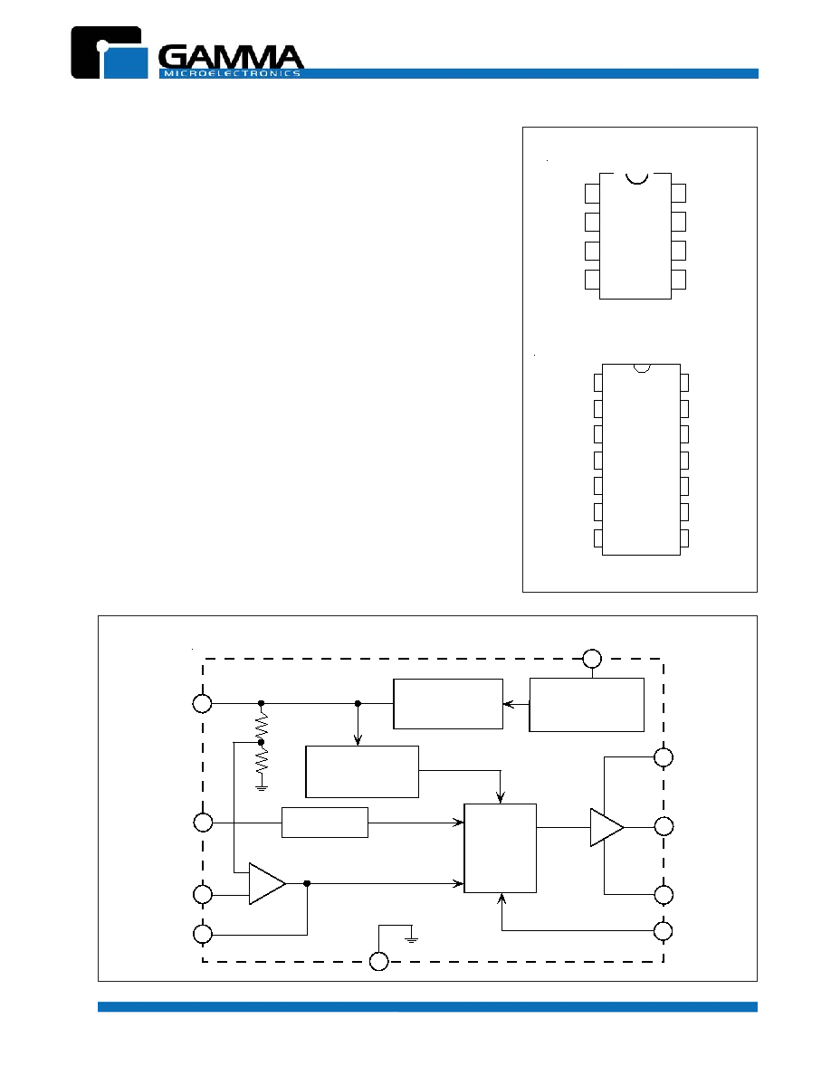
DIP-8, SOP-8 (TOP VIEW)
PIN CONNECTIONS
1
Low Start-Up and Operating Current
Automatic Feed Forward Compensation
Current Mode Operating Frequency up to 500kHz
Trimmed Oscillator Discharge Current for Precise
Duty Cycle Control
Latching PWM for Cycle-By-Cycle Current Limiting
Undervoltage Lockout with Hysteresis
High Current Totem Pole Output
1
2
3
4
8
7
6
5
V
REF
V
CC
V
FB
I
SENSE
R
T
/
C
T
COMP
GND
OUTPUT
The GM384xA series of high performance fixed-frequency current mode
PWM controllers are designed for off≠Line and DC≠to≠DC converter
applications. They require minimal external components to precisely
tailor performance in a wide variety of applications.
These GM384xA's incluide a trimmed oscillator for precise duty cycle
control, a temperature-compensated reference, high gain error amplifier,
a current-sensing comparator, and a high-current totem pole output
for driving a power MOSFET.
On-chip protection features include undervoltage lockouts with
hysteresis for both input and reference, cycle≠by≠cycle current limiting,
programmable output deadtime, and a latch for single pulse metering.
All this in a simple DIP-8 or SOP-8 package!
GM3842A and GM3844A have UVLO thresholds of 16V (on)/10V(off);
GM3843A and GM3845A have UVLO thresholds of 8.4V (on)/7.6V
(off). GM3842A and GM3843A operate within 100% duty cycle;
GM3844A and GM3845A operate within 50% duty cycle.
SIMPLIFIED BLOCK DIAGRAM
5
7
8
3
6
7
5
1
2
4
OSCILLATOR
Latc hi ng
P WM
V
R E F
Under vol tage
LOC KO U T
5. 0 V
R EF E R EN C E
V
C C
Under vol tage
LOC KO UT
R
R
+
-
Error
Amplifier
1
2
3
4
5
6
7
14
13
12
11
10
9
NC
Current Sense
OUTPUT
Power Ground
Compensation
Feedback
R
T
/C
T
GND
V
CC
8
V
REF
V
C
NC
NC
NC
SOP-14 (TOP VIEW)
GM3842A,GM3843A,GM3844A,GM3845A
HIGH PERFORMANCE CURRENT MODE PWM CONTROLLERS
Revision 1, May 2002 www.gammamicro.com
2
R
E
T
E
M
A
R
A
P
L
O
B
M
Y
S
E
U
L
A
V
S
T
I
N
U
)
e
c
r
u
o
s
e
c
n
a
d
e
p
m
i
w
o
l(
e
g
a
tl
o
V
y
l
p
p
u
S
V
C
C
0
3
V
*
k
n
i
S
r
o
e
c
r
u
o
S
,t
n
e
r
r
u
C
t
u
p
t
u
O
I
O
0
.
1
±
A
m
)
3
,
2
s
n
i
p
s
t
u
p
n
i
g
o
l
a
n
a
(
e
g
a
tl
o
V
t
u
p
n
I
V
I
5
.
5
+
o
t
3
.
0
-
V
T
(
n
o
it
a
p
i
s
s
i
D
r
e
w
o
P
m
u
m
i
x
a
M
A
)
C
∞
5
2
=
P
D
0
.
1
W
t
n
e
r
r
u
C
k
n
i
S
t
u
p
t
u
O
p
m
A
r
o
r
r
E
I
)
A
.
E
(
K
N
I
S
0
1
A
m
e
r
u
t
a
r
e
p
m
e
T
n
o
it
c
n
u
J
g
n
it
a
r
e
p
O
T
J
0
5
1
+
C
∞
e
g
n
a
R
e
r
u
t
a
r
e
p
m
e
T
e
g
a
r
o
t
S
T
g
t
s
0
5
1
+
o
t
5
6
-
C
∞
)
.
c
e
s
5
g
n
ir
e
d
l
o
s
(
e
r
u
t
a
r
e
p
m
e
T
d
a
e
L
T
L
0
6
2
C
∞
ABSOLUTE MAXIMUM RATINGS
* Note: Maximum Package Power Dissipation Limits must be observed.
PIN FUNCTIONS DESCRIPTION
N
I
P
N
O
I
T
C
N
U
F
N
O
I
T
P
I
R
C
S
E
D
1
P
M
O
C
.
n
o
it
a
s
n
e
p
m
o
c
p
o
o
l
r
o
f
e
l
b
a
li
a
v
a
e
d
a
m
s
i
d
n
a
t
u
p
t
u
o
r
e
if
il
p
m
A
r
o
r
r
E
s
i
n
i
p
s
i
h
T
2
V
B
F
e
h
t
o
t
d
e
t
c
e
n
n
o
c
y
ll
a
m
r
o
n
s
i
tI
.r
e
if
il
p
m
A
r
o
r
r
E
e
h
t
f
o
t
u
p
n
i
g
n
it
r
e
v
n
i
e
h
t
s
i
s
i
h
T
.r
e
d
i
v
i
d
r
o
t
s
i
s
e
r
a
h
g
u
o
r
h
t
t
u
p
t
u
o
y
l
p
p
u
s
r
e
w
o
p
g
n
i
h
c
ti
w
s
3
I
E
S
N
E
S
s
e
s
u
M
W
P
e
h
T
.t
u
p
n
i
s
i
h
t
o
t
d
e
t
c
e
n
n
o
c
s
i
t
n
e
r
r
u
c
r
o
t
c
u
d
n
i
o
t
l
a
n
o
it
r
o
p
o
r
p
e
g
a
tl
o
v
A
.
n
o
it
c
u
d
n
o
c
h
c
ti
w
s
t
u
p
t
u
o
e
h
t
e
t
a
n
i
m
r
e
t
o
t
n
o
it
a
m
r
o
f
n
i
s
i
h
t
4
R
T
C
/
T
g
n
it
c
e
n
n
o
c
y
b
d
e
m
m
a
r
g
o
r
p
e
r
a
e
l
c
y
c
y
t
u
d
t
u
p
t
u
O
m
u
m
i
x
a
m
d
n
a
y
c
n
e
u
q
e
r
f
r
o
t
a
ll
i
c
s
O
R
r
o
t
s
i
s
e
r
T
V
o
t
F
E
R
C
r
o
ti
c
a
p
a
c
d
n
a
T
.
e
l
b
i
s
s
o
p
s
i
z
H
k
0
0
5
o
t
n
o
it
a
r
e
p
O
.
d
n
u
o
r
g
o
t
5
D
N
G
.
d
n
u
o
r
g
r
e
w
o
p
d
n
a
y
r
ti
u
c
r
i
c
l
o
r
t
n
o
c
d
e
n
i
b
m
o
c
e
h
t
s
i
n
i
p
s
i
h
T
6
T
U
P
T
U
O
A
0
.
1
o
t
p
u
s
t
n
e
r
r
u
c
k
a
e
P
.
T
E
F
S
O
M
r
e
w
o
p
a
f
o
e
t
a
g
e
h
t
s
e
v
ir
d
y
lt
c
e
r
i
d
t
u
p
t
u
o
s
i
h
T
.
n
i
p
s
i
h
t
y
b
k
n
u
s
d
n
a
d
e
c
r
u
o
s
e
r
a
7
V
C
C
.
)
C
I
(
ti
u
c
ri
c
d
e
t
a
r
g
e
t
n
i
l
o
rt
n
o
c
e
h
t
f
o
y
l
p
p
u
s
e
v
it
i
s
o
p
e
h
t
s
i
n
i
p
s
i
h
T
8
V
F
E
R
C
r
o
ti
c
a
p
a
c
r
o
f
t
n
e
r
r
u
c
g
n
i
g
r
a
h
c
s
e
d
i
v
o
r
p
tI
.t
u
p
t
u
o
e
c
n
e
r
e
f
e
r
e
h
t
s
i
s
i
h
T
T
h
g
u
o
r
h
t
R
r
o
t
s
i
s
e
r
T
.
GM3842A,GM3843A,GM3844A,GM3845A
HIGH PERFORMANCE CURRENT MODE PWM CONTROLLERS
Revision 1, May 2002 www.gammamicro.com
3
S
C
I
T
S
I
R
E
T
C
A
R
A
H
C
L
O
B
M
Y
S
S
N
O
I
T
I
D
N
O
C
T
S
E
T
N
I
M
P
Y
T
X
A
M
T
I
N
U
n
o
i
t
c
e
S
e
c
n
e
r
e
f
e
R
e
g
a
tl
o
V
t
u
p
t
u
O
e
c
n
e
r
e
f
e
R
V
F
E
R
T
J
I
,
C
∞
5
2
=
F
E
R
A
m
1
=
9
.
4
0
.
5
1
.
5
V
n
o
it
a
l
u
g
e
R
e
n
i
L
V
F
E
R
V
2
1
V
C
C
V
5
2
0
.
6
0
2
V
m
n
o
it
a
l
u
g
e
R
d
a
o
L
V
F
E
R
A
m
1
I
F
E
R
A
m
0
2
0
.
6
5
2
V
m
t
n
e
r
r
u
C
t
u
p
t
u
O
ti
u
c
r
i
C
t
r
o
h
S
I
C
S
T
A
C
∞
5
2
=
0
0
1
-
0
8
1
-
A
m
n
o
i
t
c
e
S
r
o
t
a
ll
i
c
s
O
y
c
n
e
u
q
e
r
F
n
o
it
a
ll
i
c
s
O
f
T
J
C
∞
5
2
=
7
4
2
5
7
5
z
H
k
e
g
a
tl
o
V
h
ti
w
e
g
n
a
h
C
y
c
n
e
u
q
e
r
F
/
f
V
C
C
V
2
1
V
C
C
V
5
2
5
0
.
0
0
.
1
%
e
d
u
ti
l
p
m
A
r
o
t
a
ll
i
c
s
O
V
)
C
S
O
(
)
k
a
e
p
o
t
k
a
e
p
(
6
.
1
V
n
o
i
t
c
e
S
r
e
i
f
il
p
m
A
r
o
r
r
E
t
n
e
r
r
u
C
s
a
i
B
t
u
p
n
I
I
S
A
I
B
V
B
F
V
3
=
1
.
0
-
0
.
2
-
µ
A
e
g
a
tl
o
V
t
u
p
n
I
V
)
A
.
E
(
I
V
1
N
I
P
V
5
.
2
=
5
.
2
8
5
.
2
V
n
i
a
G
e
g
a
tl
o
V
p
o
o
L
n
e
p
O
A
L
O
V
V
2
V
O
V
4
5
6
0
9
B
d
o
it
a
R
n
o
it
c
e
j
e
R
y
l
p
p
u
S
r
e
w
o
P
P
R
S
P
V
2
1
V
C
C
V
5
2
0
6
0
7
B
d
t
n
e
r
r
u
C
k
n
i
S
t
u
p
t
u
O
I
K
N
I
S
V
2
N
I
P
V
,
V
7
.
2
=
1
N
I
P
V
1
.
1
=
2
7
A
m
t
n
e
r
r
u
C
e
c
r
u
o
S
t
u
p
t
u
O
I
E
C
R
U
O
S
V
2
N
I
P
V
,
V
3
.
2
=
1
N
I
P
V
5
=
5
.
0
-
0
.
1
-
A
m
e
g
a
tl
o
V
t
u
p
t
u
O
h
g
i
H
V
H
O
V
2
N
I
P
k
5
1
=
L
R
,
V
3
.
2
=
D
N
G
o
t
0
.
5
0
.
6
V
e
g
a
tl
o
V
t
u
p
t
u
O
w
o
L
V
L
O
V
2
N
I
P
k
5
1
=
L
R
,
V
7
.
2
=
8
n
i
P
o
t
8
.
0
1
.
1
V
n
o
i
t
c
e
S
e
s
n
e
S
t
n
e
r
r
u
C
n
i
a
G
G
V
)
2
d
n
a
1
e
t
o
N
(
5
8
.
2
0
.
3
5
1
.
3
V
/
V
l
a
n
g
i
S
t
u
p
n
I
m
u
m
i
x
a
M
V
)
X
A
M
(I
V
1
N
I
P
)
1
e
t
o
N
(
V
5
=
9
.
0
0
.
1
1
.
1
V
n
o
it
c
e
j
e
R
e
g
a
tl
o
V
y
l
p
p
u
S
R
V
S
V
2
1
V
C
C
)
1
e
t
o
N
(
V
5
2
0
7
B
d
t
n
e
r
r
u
C
s
a
i
B
t
u
p
n
I
I
S
A
I
B
V
3
N
I
P
V
3
=
0
.
3
-
0
1
-
µ
A
n
o
i
t
c
e
S
t
u
p
t
u
O
e
g
a
tl
o
V
t
u
p
t
u
O
w
o
L
V
L
O
I
K
N
I
S
A
m
0
2
=
8
0
.
0
4
.
0
V
I
K
N
I
S
A
m
0
0
2
=
4
.
1
2
.
2
V
e
g
a
tl
o
V
t
u
p
t
u
O
h
g
i
H
V
H
O
I
K
N
I
S
A
m
0
2
=
3
1
5
.
3
1
V
I
K
N
I
S
A
m
0
0
2
=
2
1
3
1
V
e
m
i
T
e
s
i
R
t
R
T
J
C
,
C
∞
5
2
=
L
)
3
e
t
o
N
(
F
n
1
=
5
4
0
5
1
S
n
e
m
i
T
ll
a
F
t
F
T
J
C
,
C
∞
5
2
=
L
)
3
e
t
o
N
(
F
n
1
=
5
3
0
5
1
S
n
n
o
i
t
c
e
S
t
u
o
k
c
o
L
e
g
a
t
l
o
v
r
e
d
n
U
d
l
o
h
s
e
r
h
T
t
r
a
t
S
V
)
T
S
(
H
T
A
4
4
8
3
M
G
,
A
2
4
8
3
M
G
5
.
4
1
0
.
6
1
5
.
7
1
V
A
5
4
8
3
M
G
,
A
3
4
8
3
M
G
8
.
7
4
.
8
0
.
9
V
e
g
a
tl
o
V
g
n
it
a
r
e
p
O
m
u
m
i
n
i
M
)
N
O
n
r
u
t
r
e
tf
a
(
V
)
N
I
M
(
R
P
O
A
4
4
8
3
M
G
,
A
2
4
8
3
M
G
5
.
8
0
1
5
.
1
1
V
A
5
4
8
3
M
G
,
A
3
4
8
3
M
G
0
.
7
6
.
7
2
.
8
V
n
o
i
t
c
e
S
M
W
P
e
l
c
y
C
y
t
u
D
m
u
m
i
x
a
M
D
)
X
A
M
(
A
3
4
8
3
M
G
,
A
2
4
8
3
M
G
5
9
7
9
0
0
1
%
A
5
4
8
3
M
G
,
A
4
4
8
3
M
G
7
4
8
4
0
5
%
e
l
c
y
C
y
t
u
D
m
u
m
i
n
i
M
D
M
(
N
I
)
0
%
t
n
e
r
r
u
C
y
b
d
n
a
t
S
l
a
t
o
T
t
n
e
r
r
u
C
p
U
-
t
r
a
t
S
I
T
S
7
1
.
0
3
.
0
A
m
t
n
e
r
r
u
C
y
l
p
p
u
S
g
n
it
a
r
e
p
O
I
)
R
P
O
(
C
C
V
3
N
I
P
V
=
2
N
I
P
V
0
=
3
1
7
1
A
m
e
g
a
tl
o
V
r
e
n
e
Z
V
Z
I
C
C
A
m
5
2
=
0
3
8
3
V
ELECTRICAL CHARACTERISTICS
(T
A
= 0∞C to 70∞ C, *V
CC
=15V, C
T
=3.3nF, R
T
=10k
,
unless otherwise specified )
* Adjust V
CC
above the Startup threshold before setting to 15 V.
Note1: Parameter measured at trip point of latch with V
PIN2
= 0.
Note2: Gain defined as A=
V
PIN1
/
V
PIN3
; 0
V
PIN3
0.8V
Note3: These parameters, although guaranteed, are not 100% tested in production
GM3842A,GM3843A,GM3844A,GM3845A
HIGH PERFORMANCE CURRENT MODE PWM CONTROLLERS
Revision 1, May 2002 www.gammamicro.com
4
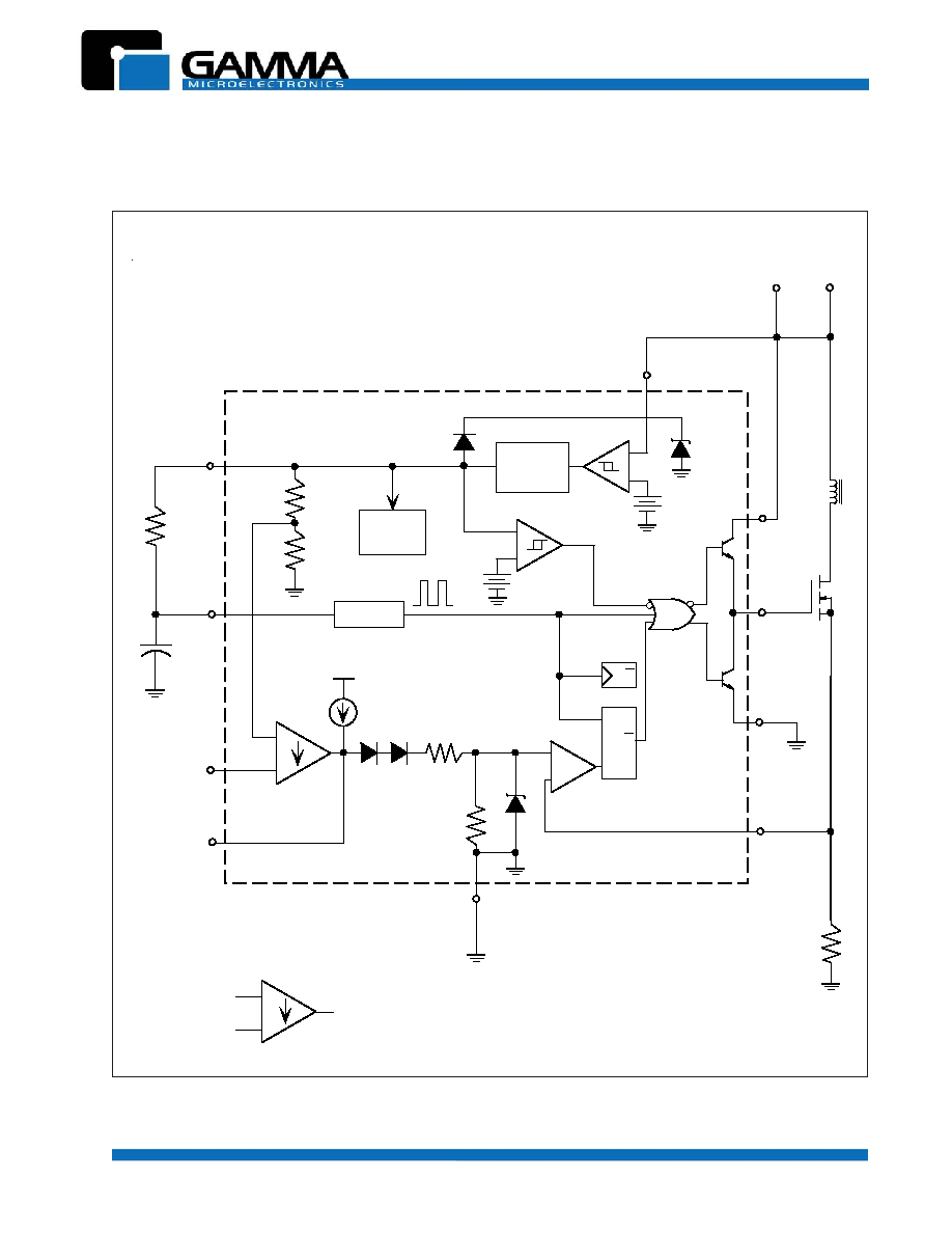
REPRESENTATIVE BLOCK DIAGRAM
+
Oscillator
R
R
+
-
Internal
Bias
Reference
Regulator
+
-
-
+
-
-
+
+
-
+
+
-
Sink Only
Positive True Logic
=
C
T
R
T
1
2
4
Vref
8
2.5V
Error
Amplifier
1.0mA
2R
R
1.0V
Current Sense
Comparator
S
R
Q
Q
T
PWM Latch
Vcc
UVLO
3.6V
Vref
UVLO
36V
Vcc
Vcc
Vin
Vc
7
Q1
7
Output
6
Power
Ground
5
Current
Sense
Input
3
GND 5
Rs
Output
Compensation
Voltage
Feedback
Input

GM3842A,GM3843A,GM3844A,GM3845A
HIGH PERFORMANCE CURRENT MODE PWM CONTROLLERS
Revision 1, May 2002 www.gammamicro.com
5
The GM3842A, GM3843A, GM3844A and GM3845A
are high performance, fixed frequency, current mode
controllers. They are designed for off≠line and DC≠to≠
DC converter applications offering great versatility with
minimal external components. A representative block
diagram is shown on page 4.
Oscillator
The oscillator frequency is determined by the values of
the timing components R
T
and C
T
. Capacitor C
T
is
charged from the 5.0 V reference through resistor R
T
to
approximately 2.8 V and discharged to 1.2 V by an
internal current sink. As C
T
discharges, the oscillator
generates an internal blanking pulse that holds the
center input of the NOR gate high. This causes the
output to be in a low state, and produces a controlled
amount of output deadtime.
Many different values of R
T
and C
T
will give the same
oscillator frequency, but only one combination will yield
a specific output deadtime at a given frequency. The
oscillator thresholds are temperature-compensated;
discharge current is trimmed and guaranteed to within
±10% at T
J
= 25∞C. Thiw minimizes variations of
oscillator frequency and maximum output duty cycle.
In many noise sensitive applications it may be desirable
to frequency≠lock the converter by applying a clock
signal to the circuit shown in Figure 1. For best locking
results, set the free≠running oscillator frequency to about
10% less than the clock frequency. A method for multi
unit synchronization is shown in Figure 2. You can get
very accurate output duty cycle clamping by tweaking
the clock waveform..
Error Amplifier
The GM384xA's have a fully compensated error amplifier
with access to both the inverting input and output,
providing DC voltage gain of 90 dB (typical). The
noninverting input is internally biased at 2.5 V and is
not pinned out. The converter output voltage is typically
divided down and monitored by the inverting input. The
maximum input bias current is ≠2.0 mA which can cause
an output voltage error that is equal to the product of
the input bias current and the equivalent input divider
source resistance.
The Error Amplfier Output (Pin 1) allows external loop
compensation. The output voltage is offset by the two
diode drops (
1.4 V) and divided by three before
connecting to the inverting input of the Current Sense
Comparator. This assures that no drive pulses appear
at the Output (Pin 6) when Pin 1 is at its lowest state
(V
OL
). This happens when the power supply is operating
and the load is removed, or at the beginning of a soft≠
start interval (Figures 4, 5). The Error Amp minimum
feedback resistance is limited by the amplifier's source
current (0.5 mA) and the required output voltage (V
OH
)
to reach the comparator's 1.0 V clamp level:
R
F(min)
= 8800
3.0 (1.0 V) + 1.4 V
0.5 mA
Current Sense Comparator and PWM Latch
The GM384xA's operate as a current mode controller,
whereby output switch conduction is initiated by the
oscillator and terminated when the peak inductor current
reaches the threshold level established by the Error
Amplifier Output/Compensation (Pin1). The error signal
controls the peak inductor current cycle≠by≠cycle. The
Current Sense Comparator PWM Latch configuration
assures that only a single pulse appears at the Output
during any given oscillator cycle. The inductor current
is converted to a voltage by inserting the ground-
referenced sense resistor R
S
in series with the source
of output switch Q1. This voltage is monitored by the
Current Sense Input (Pin 3) and compared to a level
derived from the Error Amp Output. The peak inductor
current under normal operating conditions is controlled
by the voltage at pin 1 where:
I
pk
=
V
(Pin 1)
≠ 1.4 V
3 R
S
When the power supply output is overloaded or if output
voltage sensing is lost, the chip operation is not normal.
In these situations, the Current Sense Comparator
threshold will be internally clamped to 1.0 V and the
maximum peak switch current is:
I
pk(max)
=
1.0V
R
S
OPERATING DESCRIPTION